Bilayer Light-Emitting Electrochemical Cells for Signage and Lighting Applications

Linköping Studies in science and technology Dissertation No. 1582
Light-Emitting Electrochemical Transistors
Jiang Liu
Laboratory for Organic Electronics
Department of Science and Technology (ITN)
Linköpings Universitet, SE-601 74 Norrköping, Sweden
Norrköping 2014
Light-Emitting Electrochemical Transistors
Jiang Liu
Linköping Studies in Science and Technology. Dissertation No. 1582
Copyright © 2014 Jiang Liu
Printed by LiU-Tryck, Linköping, Sweden, 2014
ISBN: 978-91-7519-382-3
ISSN: 0345-7524
ABSTRACT Since the discovery of conductive polymers in 1977, the implementation
of organic conjugated materials in electronic applications has been of
great interest in both industry and academia. The goal of organic
electronics is to realize large-area, inexpensive and mechanically-
flexible electronic applications.
Organic light emitting diodes (OLEDs), as the first commercial product
made from organic conjugated polymers, have successfully
demonstrated that organic electronics can make possible a new
generation of modern electronics. However, OLEDs are highly sensitive
to materials selection and requires a complicated fabrication process.
As a result, OLEDs are expensive to fabricate and are not suitable for
low-cost printing or roll-to-roll process.
This thesis studies an alternative to OLEDs: light-emitting electrochemical
cells (LECs). The active materials in an LEC consist of a conjugated light-
emitting polymer (LEP) and an electrolyte. Taking advantage of
electrochemical doping of the LEP, an LEC features an in-situ formed
emissive organic p-n junction which is easy to fabricate. We aim to
control the electrochemical doping profile by employing a “gate”
terminal on top of a conventional LEC, forming a light-emitting
electrochemical transistor (LECT). We developed three generations of
LECTs, in which the position of the light-emitting profile can be modified
by the voltage applied at the gate electrode, as well as the geometry
of the gate materials. Thus, one can use this structure to achieve a
centered light-emitting zone to maximize the power-conversion
efficiency. Alternatively, LECTs can be used for information display in a
highly integrated system, as it combines the simultaneous modulation of
photons and electrons.
In addition, we use multiple LECs to construct reconfigurable circuits,
based on the reversible electrochemical doping. We demonstrate an
LEC-array where several different circuits can be created by forming
diodes with different polarity at different locations. The thereby formed
circuitry can be erased and turned into circuitry with other functionality.
For example, the diodes of a digital AND gate can be re-programmed
to form an analogue voltage limiter. These reprogrammable circuits are
promising for fully-printed and large-area reconfigurable circuits with
facile fabrication.
SVENSK SAMMANFATTNING AV AVHANDLINGEN
Allt sedan upptäckten av elektriskt ledande polymerer 1977 har
konjugerade organiska material för elektroniska tillämpningar rönt stort
intresse både i den industriella och den akademiska världen. Ett viktigt
mål med organisk elektronik är att realisera elektronik som kan täcka
stora ytor samtidigt som den är mekaniskt flexibel och billig att tillverka.
Organiska lysdioder (OLEDs) är den första kommersiella produkten som
bygger på konjugerade polymerer, och har förtjänstfullt visat att
organisk elektronik möjliggör en ny generation av modern elektronik.
OLEDs är dock känsliga för materialval och kräver en relativt
komplicerad tillverkningsprocess. De är därigenom inte lämpliga för
rulle-till-rulle-tillverkning med kostnadseffektiva tryckmetoder.
Denna avhandling behandlar ett alternativ till OLEDs: ljusemitterande
elektrokemiska celler (LECs). De aktiva materialen i en LEC är en
ljusemitterande polymer (LEP) och en elektrolyt. Tillverkningsproceduren
är enkel och funktionen bygger på att en ljusemitterande p-n-övergång
formas genom elektrokemisk dopning av polymeren. I avhandlingen
presenteras en metod att kontrollera dopningsprofilen genom att tillföra
en gate-elektrod ovanpå en konventionell LEC och därigenom skapa
en ljusemitterande elektrokemisk transistor (LECT). Vi har utvecklat tre
generationer av denna LECT, där positionen hos den ljusemitterande
zonen kan regleras såväl genom applicerad spänning på gate-
elektroden som genom geometrin hos densamma. På så vis kan en
centrerad ljusemitterande zon åstadkommas, vilket maximerar
energieffektiviteten hos komponenten. LECTs har även potential att
användas i displayer i integrerade system, eftersom de kombinerar
funktionaliteten hos en transistor med möjligheten att emittera ljus.
Utöver det ovanstående har multipla LECs använts för att konstruera
programmerbara kretsar, baserade på reversibiliteten hos den
elektrokemiska dopningen. En LEC-array demonstreras, där flera olika
kretsar kan realiseras genom att dioder med olika polaritet skapas
elektriskt i olika positioner. När en sådan krets har använts, kan den
raderas och därefter omprogrammeras till en ny funktionalitet.
Exempelvis kan dioderna i en digital AND-krets programmeras om till att
istället forma en analog spänningsbegränsare. Dessa programmerbara
kretsar är enkla att tillverka och är därför ett lovande koncept för tryckt
elektronik på stora ytor.

ACKNOWLEDGEMENTS
Above all, I want to thank my co-supervisor Isak Engquist, for your
guidance, encouragement as well as your trust and patience in me
throughout the past years. I would also like to thank you for being an
open person to ideas, and for encouraging and helping me to shape
my interest and ideas. This dissertation would not have been possible
without your help.
I would like to thank my main supervisor Magnus Berggren, for your
inspiring enthusiasm, optimism and invaluable scientific input,
specifically, for your bright solution to that obstacle that I had been stuck
with for two years in the first LECT project.
I also want to thank Tom Aernouts in IMEC, who introduced me to the
research field of organic electronics, and who helped me in the TEM
measurement for the transistor project.
I want to thank every member of Organic Electronics Group and Acreo
for creating such a friendly and working atmosphere, with
special thanks to:
Xavier, for your help in interpreting all the tricky physics, from inspiring
talks and the course you gave.
Sophie, for all the kind help in administration work and daily life.
Lasse and Bengt, for all the handicraft work in the lab.
Ek, for your jokes and warm friendship, for the help in work and, more
importantly, in daily life.
cheerful

Hiam and Olga, for sharing the joy and complaints in the same office. I
hope both of you can make it to my dissertation.
Amanda, Björn, Elina, Henrik, Loïg, Negar, Skomantas, Simone and Zia,
for the joyful moments we shared outside work, for the songs we sang
from Lucia tåg, for the sweat dripped imn the football field and ice ring,
for the nature we explored in the kayaks, and for the laughers in all the
parties.
Dan, Jun and Hui, for being my Asian companion and sharing my
nostalgia in the same(or similar) language.
Finally, I would like to thank my dear love, Linjing Fu, who has provided
me with care, passion and support, and who has shared with me all the
joy and frustration during the last few years. Furthermore, I would also like
to thank my parents for their endless love.
February 16, 2014 in Norrköping
Jiang Liu
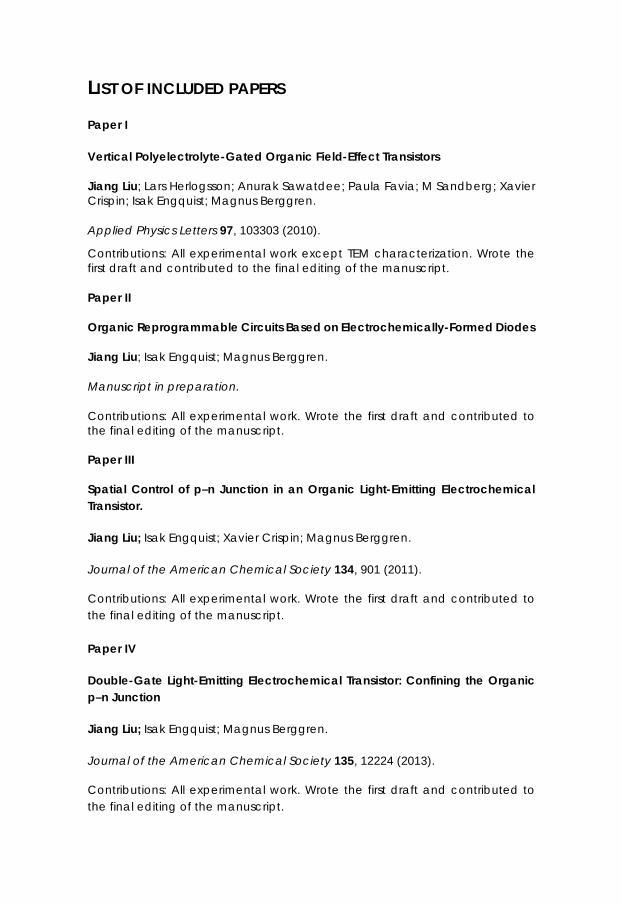
LIST OF INCLUDED PAPERS
Paper I
Vertical Polyelectrolyte-Gated Organic Field-Effect Transistors
Jiang Liu; Lars Herlogsson; Anurak Sawatdee; Paula Favia; M Sandberg; Xavier Crispin; Isak Engquist; Magnus Berggren.
Applied Physics Letters 97, 103303 (2010).
Contributions: All experimental work except TEM characterization. Wrote the first draft and contributed to the final editing of the manuscript.
Paper II
Organic Reprogrammable Circuits Based on Electrochemically-Formed Diodes
Jiang Liu; Isak Engquist; Magnus Berggren.
Manuscript in preparation.
Contributions: All experimental work. Wrote the first draft and contributed to the final editing of the manuscript. Paper III
Spatial Control of p–n Junction in an Organic Light-Emitting Electrochemical Transistor.
Jiang Liu; Isak Engquist; Xavier Crispin; Magnus Berggren.
Journal of the American Chemical Society 134, 901 (2011). Contributions: All experimental work. Wrote the first draft and contributed to the final editing of the manuscript. Paper IV
Double-Gate Light-Emitting Electrochemical Transistor: Confining the Organic p–n Junction
Jiang Liu; Isak Engquist; Magnus Berggren.
Journal of the American Chemical Society 135, 12224 (2013). Contributions: All experimental work. Wrote the first draft and contributed to the final editing of the manuscript.

Paper V
Half-Gate Light-Emitting Electrochemical Transistor to Achieve Centered Emissive Organic p-n Junction
Jiang Liu; Isak Engquist; Magnus Berggren.
Manuscript in preparation.
Contributions: All experimental work. Wrote the first draft and contributed to the final editing of the manuscript.
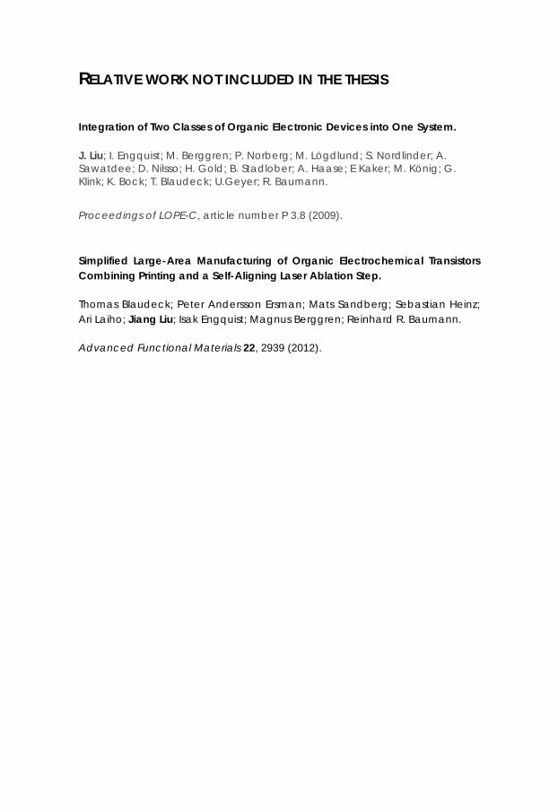
RELATIVE WORK NOT INCLUDED IN THE THESIS
Integration of Two Classes of Organic Electronic Devices into One System.
J. Liu; I. Engquist; M. Berggren; P. Norberg; M. Lögdlund; S. Nordlinder; A. Sawatdee; D. Nilsso; H. Gold; B. Stadlober; A. Haase; E Kaker; M. König; G. Klink; K. Bock; T. Blaudeck; U.Geyer; R. Baumann. Proceedings of LOPE-C, article number P 3.8 (2009).
Simplified Large-Area Manufacturing of Organic Electrochemical Transistors Combining Printing and a Self-Aligning Laser Ablation Step.
Thomas Blaudeck; Peter Andersson Ersman; Mats Sandberg; Sebastian Heinz; Ari Laiho; Jiang Liu; Isak Engquist; Magnus Berggren; Reinhard R. Baumann.
Advanced Functional Materials 22, 2939 (2012).

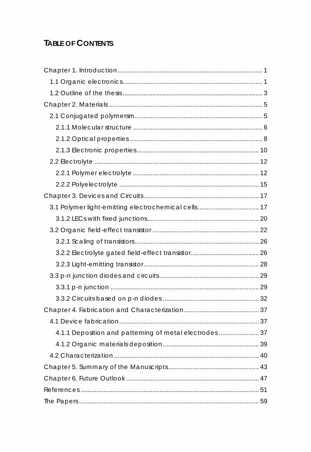
TABLE OF CONTENTS
Chapter 1. Introduction ................................................................................... 1
1.1 Organic electronics ................................................................................ 1
1.2 Outline of the thesis ................................................................................ 3
Chapter 2. Materials ........................................................................................ 5
2.1 Conjugated polymersm ......................................................................... 5
2.1.1 Molecular structure .......................................................................... 6
2.1.2 Optical properties ............................................................................ 8
2.1.3 Electronic properties ...................................................................... 10
2.2 Electrolyte .............................................................................................. 12
2.2.1 Polymer electrolyte ........................................................................ 12
2.2.2 Polyelectrolyte ................................................................................ 15
Chapter 3. Devices and Circuits .................................................................. 17
3.1 Polymer light-emitting electrochemical cells ................................... 17
3.1.2 LECs with fixed junctions ................................................................ 20
3.2 Organic field-effect transistor ............................................................. 22
3.2.1 Scaling of transistors ....................................................................... 26
3.2.2 Electrolyte gated field-effect transistor ....................................... 26
3.2.3 Light-emitting transistor .................................................................. 28
3.3 p-n junction diodes and circuits ......................................................... 29
3.3.1 p-n junction ..................................................................................... 29
3.3.2 Circuits based on p-n diodes ....................................................... 32
Chapter 4. Fabrication and Characterization ........................................... 37
4.1 Device fabrication ................................................................................ 37
4.1.1 Deposition and patterning of metal electrodes ....................... 37
4.1.2 Organic materials deposition ....................................................... 39
4.2 Characterization ................................................................................... 40
Chapter 5. Summary of the Manuscripts .................................................... 43
Chapter 6. Future Outlook ............................................................................ 47
References ...................................................................................................... 51
The Papers ....................................................................................................... 59


1
Chapter 1. Introduction
1.1 ORGANIC ELECTRONICS
Since the invention of transistors in 1947, integrated circuits based on
silicon transistors have monumentally impacted our society. As Moore's
law says, the number of transistors on integrated circuits doubles every
18 months(1). Nowadays in a personal computer the transistor count has
exceeded 5 billion. With the silicon technology continuing to
revolutionize our world, other materials science has been developed to
introduce new functional electronics that silicon chips cannot offer.
Organic electronics uses organic conjugated materials as the core
materials in electronic devices and systems. The unique properties that
organic materials possess open new routes for electronic applications.
First of all, most organic materials can be dissolved into solution. This
makes it possible to use conventional “printing” techniques to fabricate

2
organic devices, which leads to large-area, inexpensive processing
methods.
Secondly, polymers can be deposited onto flexible substrates such as
paper or plastic, and flexible organic solar cells as well as stretchable
light-emitting components have already been demonstrated.
Moreover, organic materials are mainly composed of carbon and
hydrogen atoms with addition of other elements such as nitrogen,
oxygen, phosphorus etc., which is essentially the same as many
biological molecules. Thus, organic electronics can be made to be
highly biocompatible when integrating into biological systems.
Last but not least, organic molecules can be synthesized with unlimited
variations. A single molecule can be made to function as a resistor, an
insulator or even a rectifier. Building more complex electronic systems
from multiple organic molecules is still a great challenge but it provides
a potential approach to extend beyond the physical limitations of silicon
technologies.
The organic light-emitting diode (OLED) was the first commercial
electronic component made from organic materials. Products
incorporating OLEDs range from mobile phones’ displays to TV panels,
which are already existing in the market. As an alternative product to
OLED, the light-emitting electrochemical cell (LEC) shows similar
electroluminescent behavior with a simpler structure; LECs are also more

3
versatile due to their reversible electrochemical system. In this thesis the
main focus is on LECs, and the aim is to exploit new functionalities of
these components.
1.2 OUTLINE OF THE THESIS
The thesis is structured as follows: Chapter 2 introduces organic
semiconductors and electrolytes which are essential in the materials
system; in chapter 3 a variety of organic devices such as transistors and
LECs are discussed, together with related circuit constructions; chapter
4 introduces the fabrication and characterization methods to realize
those devices. Following that, chapter 5 summarizes the manuscripts
and chapter 6 provides an outlook towards future perspectives.

4
5
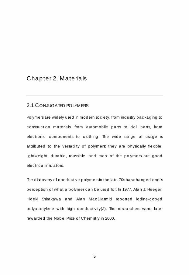
Chapter 2. Materials
2.1 CONJUGATED POLYMERS
Polymers are widely used in modern society, from industry packaging to
construction materials, from automobile parts to doll parts, from
electronic components to clothing. The wide range of usage is
attributed to the versatility of polymers: they are physically flexible,
lightweight, durable, reusable, and most of the polymers are good
electrical insulators.
The discovery of conductive polymers in the late 70s has changed one’s
perception of what a polymer can be used for. In 1977, Alan J. Heeger,
Hideki Shirakawa and Alan MacDiarmid reported iodine-doped
polyacetylene with high conductivity(2). The researchers were later
rewarded the Nobel Prize of Chemistry in 2000.

6
2.1.1 MOLECULAR STRUCTURE
To understand the origin of conductivity in polymers, one must look at
the molecular structure. As the most common materials in conventional
plastic bags(3), polyethylene has a repeating unit of -(CH2)n-, as
depicted in figure 2.1b. Each carbon atom in polyethylene has four sp3
molecular orbitals and bonds to the adjacent four atoms by strong σ
bonds. In those orbitals, the valance electrons are highly localized; thus
no free charge carrier is present, which is reflected by the fact that the
energy difference between the valance band and the conduction
band is as large as 8 eV(4). This large band gap is the reason why
polyethylene is transparent and nonconductive.
Figure 2.1 (a) plastic bags made from polyethylene; (b) the chemical
structure of polyethylene.
As the first organic material known to be conductive, polyacetylene (the
chemical structure shown in figure 2.2a possesses carbon atoms which
have three sp2 molecular orbitals and one pz orbital. The three electrons
in sp2 molecular orbitals form three σ bonds which connects two
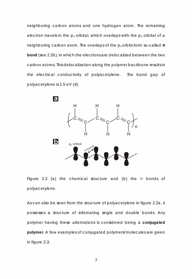
7
neighboring carbon atoms and one hydrogen atom. The remaining
electron travels in the pz orbital, which overlaps with the pz orbital of a
neighboring carbon atom. The overlaps of the pz orbits form so-called π
bond (see 2.2b), in which the electrons are delocalized between the two
carbon atoms. This delocalization along the polymer backbone results in
the electrical conductivity of polyacetylene. The band gap of
polyacetylene is 1.5 eV (4).
Figure 2.2 (a) the chemical structure and (b) the π bonds of
polyacetylene.
As can also be seen from the structure of polyacetylene in figure 2.2a, it
possesses a structure of alternating single and double bonds. Any
polymer having these alternations is considered being a conjugated
polymer. A few examples of conjugated polymers/molecules are given
in figure 2.3.

8
Figure 2.3 Examples of conjugated materials.
2.1.2 OPTICAL PROPERTIES
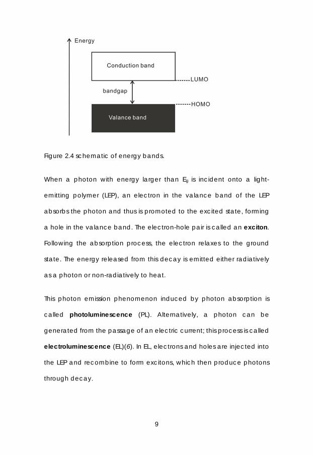
The repeat unit of a conjugated polymer interacts with its neighboring
units, creating the electronic bands(5). The highest occupied levels of
the electronic bands construct the valence band, and the lowest
unoccupied levels constitute the conduction band. The edge of the
valence band and the edge of the conduction band are termed HOMO
(highest occupied molecular orbital) and LUMO (lowest unoccupied
molecular orbital), respectively; see figure 2.4. The energy difference
between LUMO and HOMO defines the bandgap (Eg) of the polymer.
9
Figure 2.4 schematic of energy bands.
When a photon with energy larger than Eg is incident onto a light-
emitting polymer (LEP), an electron in the valance band of the LEP
absorbs the photon and thus is promoted to the excited state, forming
a hole in the valance band. The electron-hole pair is called an exciton.
Following the absorption process, the electron relaxes to the ground
state. The energy released from this decay is emitted either radiatively
as a photon or non-radiatively to heat.
This photon emission phenomenon induced by photon absorption is
called photoluminescence (PL). Alternatively, a photon can be
generated from the passage of an electric current; this process is called
electroluminescence (EL)(6). In EL, electrons and holes are injected into
the LEP and recombine to form excitons, which then produce photons
through decay.

10
2.1.3 ELECTRONIC PROPERTIES
Although free charge carriers are present in pristine conjugated
polymers, their conductivity is usually low. Typical values of conductivity
in pristine conjugated polymers are in the range of 10-10 to 10-5 S/m.
Doping is commonly used to boost the conductivity by a few orders of
magnitude, and is usually achieved by introducing impurities into the
intrinsic polymer.
Doping can be seen as removal of electrons from the polymer chain (p-
doping or oxidation) or addition of electrons onto the polymer (n-doping
or reduction). Assume that an electron is removed from a conjugated
polymer chain. A positive mobile charge is in this case created, which
induces distortion of the local lattice. This free charge together with local
distortion is called a polaron, which carries a spin of ½. The energy level
of the polaron is situated in the bandgap of the polymer, as shown in
figure 2.5b. One polaron can be delocalized over a few repeat units of
a polymer chain.
Removing a second electron would create another polaron. When two
polarons are close enough the distortion is shared, creating a bipolaron.
A bipolaron is thermodynamically more stable than two single polarons
and it has zero spin. The band structure of the bipolaron is depicted in
figure 2.5c.

11
High oxidation level creates more bipolarons and the overlap of
bipolaron states leads to the formation of a bipolaron band; see figure
2.5d. A widened bandgap also results because the electrons that form
the bipolaron bands are taken from the edge of valance band.
Figure 2.5 Illustration of the band structure of a polymer as the doping
level increases.
Doping can be performed by various methods. The first example of a
conductive polymer was made by exposing polyacetylene to oxidizing
or reducing agents. Such a redox process is characterized as chemical
doping.
Conjugated polymers can also be doped electrochemically. In
electrochemical doping, an electric current is driven through the
polymer, and the surrounding ions migrate into the soft and porous
polymer chain to compensate the injected charge. As a result, the

12
polymer can be n-doped or p-doped depending on the polarity of the
ions:
: →
: →
where p0, p- and p+ represents neutral, n-doped and p-doping polymer
respectively, C+ and A- indicates cation and anion.
2.2 ELECTROLYTE
An electrolyte is a substance that consists of ionizable compounds when
dissolved in a solvent. A classic example is NaCl dissolved in water
solution. Electrolyte is a vital component inside the human body, as it
conducts various minerals (ions) and regulates biological functions, such
as muscle contraction and neuron activities. In industry, electrolytes are
widely used in energy storage applications, such as lithium batteries and
fuel cells. In this section we discuss electrolytes in the form of ionically
conductive polymers.
2.2.1 POLYMER ELECTROLYTE
A polymer electrolyte consists of a salt that is dissolved in a polymer host.
It was first discovered by Fenton in 1973, who observed that polyethylene
oxide(PEO) can be used to dissolve and conduct alkali salt(7).

13
Ion conductivity in polymer electrolytes is governed by the fact that ions
move between many co-ordinate sites induced by the local movement
of the chain segments of the polymer host(8). It is generally believed that
in such systems, it is more energetically favorable that the cations form
co-ordinate bonds to the polymer backbone, while the anions diffuse
freely(9). Therefore, it is desirable for the polymer host to possess a strong
electron donor group so that it forms a strong coordination bond to the
cations. PEO with a repeating oxygen group, which is a strong electron
donor, is the most commonly used polymer in polymer electrolytes. It has
a chemical structure of –(CH2CH2O)n– , as shown in figure 2.6a. It also has
a distance between neighboring oxygen groups that is ideal for ion
transportation, evidenced by the fact that both –(CH2O)n– and –
(CH2CH2CH2O)n– show lower ion conductivity(10).
Figure 2.6b shows a schematic of ion transportation in PEO-based
electrolytes. As the cation moves from one co-ordinate site to another,
its movement is assisted by the segmental motion in the PEO chain (11,
12). It is believed that the ionic transport is closely correlated to the
flexibility of the polymer host backbone, therefore the ion conductivity is
highly dependent on temperature. Indeed, below the glass transition
temperature (Tg), PEO is crystalline and the ion conductivity is negligible.
In contrast, above Tg PEO is amorphous and flexible, displaying a
relatively high ion conduction capability. The conductivity-temperature
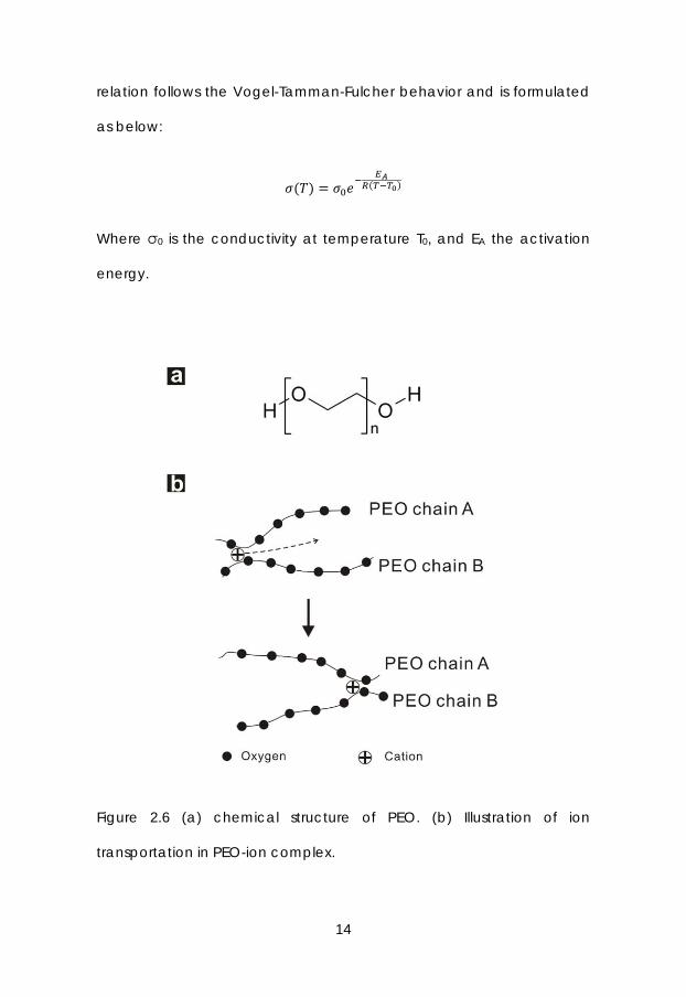
14
relation follows the Vogel-Tamman-Fulcher behavior and is formulated
as below:
Where σ0 is the conductivity at temperature T0, and EA the activation
energy.
Figure 2.6 (a) chemical structure of PEO. (b) Illustration of ion
transportation in PEO-ion complex.
15
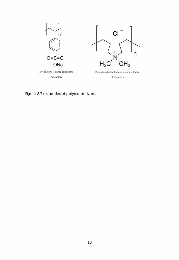
2.2.2 POLYELECTROLYTE
Polyelectrolytes are polymers bearing ionic groups. This ionic group
would dissociate while dissolving in a solvent, leading to a charged
polymer backbone and mobile ions with opposite charges. A
polyelectrolyte possessing anionic groups is termed polycation because
the polymer backbone is positively charged, while the one carrying
cationic groups is called polyanion. Examples of polyelectrolytes are
shown in figure 2.7.
In the solid state, the polymer backbone is considered immobile due to
its large size, while the counter ions are relatively freer to move. Because
polyelectrolytes are mostly hygroscopic, the solid state electrolytes
usually contain a certain amount of water in ambient atmosphere. Upon
the dissociation of counter ions from the polymer backbones, solvent
molecules form a shell surrounding each counter ion and move together
with them. Therefore, the ion conductivity in a polyelectrolyte depends
on the viscosity of the solvent, the size of the counter ions and the
amount of solvent in the materials system, with the latter parameter
being heavily influenced by the humidity level(13).
16
Figure 2.7 examples of polyelectrolytes.

17
Chapter 3. Devices and Circuits
In this chapter we review various devices and circuits that are
mentioned in paper I-V.
3.1 POLYMER LIGHT-EMITTING ELECTROCHEMICAL CELLS
A light-emitting electrochemical cell (LEC) is a two terminal
electrochemical device that generates light through
electroluminescence. The first LEC was invented by Pei et al. in 1995(14),
and LECs have attracted great research attention ever since(15-48). The
conventional LEC consists merely of a layer of active materials
sandwiched by two charge-injection electrodes. The active material is
an intermixture of an LEP and an electrolyte.
As displayed in figure 3.1, an LEC can be structured according to
different geometries. The most conventional LEC is constructed in a
vertical manner, where the cathode/active material/anode are
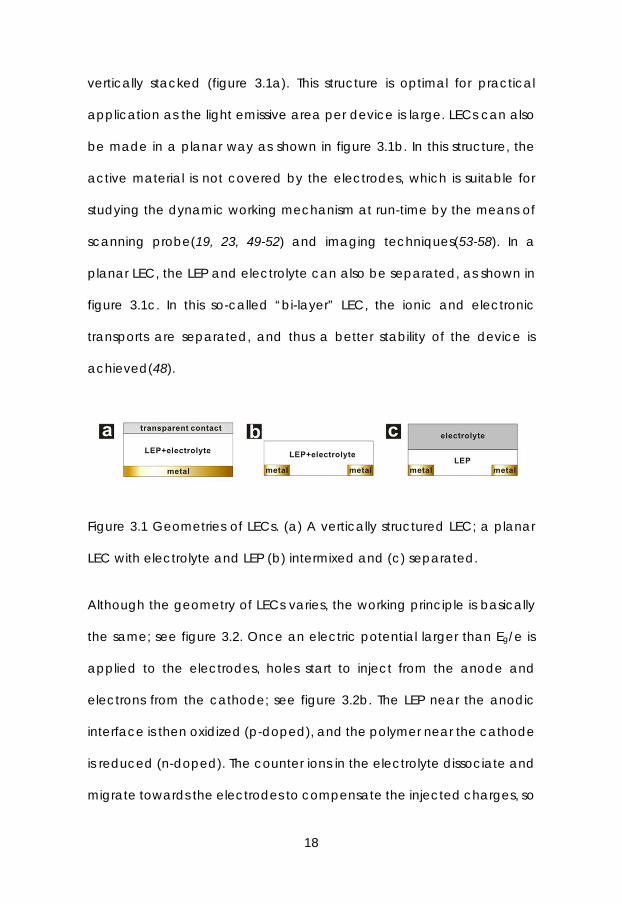
18
vertically stacked (figure 3.1a). This structure is optimal for practical
application as the light emissive area per device is large. LECs can also
be made in a planar way as shown in figure 3.1b. In this structure, the
active material is not covered by the electrodes, which is suitable for
studying the dynamic working mechanism at run-time by the means of
scanning probe(19, 23, 49-52) and imaging techniques(53-58). In a
planar LEC, the LEP and electrolyte can also be separated, as shown in
figure 3.1c. In this so-called “bi-layer” LEC, the ionic and electronic
transports are separated, and thus a better stability of the device is
achieved(48).
Figure 3.1 Geometries of LECs. (a) A vertically structured LEC; a planar
LEC with electrolyte and LEP (b) intermixed and (c) separated.
Although the geometry of LECs varies, the working principle is basically
the same; see figure 3.2. Once an electric potential larger than Eg/e is
applied to the electrodes, holes start to inject from the anode and
electrons from the cathode; see figure 3.2b. The LEP near the anodic
interface is then oxidized (p-doped), and the polymer near the cathode
is reduced (n-doped). The counter ions in the electrolyte dissociate and
migrate towards the electrodes to compensate the injected charges, so
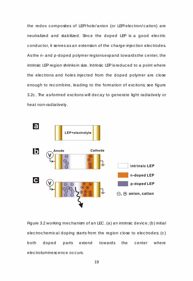
19
the redox composites of LEP/hole/anion (or LEP/electron/cation) are
neutralized and stabilized. Since the doped LEP is a good electric
conductor, it serves as an extension of the charge-injection electrodes.
As the n- and p-doped polymer regions expand towards the center, the
intrinsic LEP region shrinks in size. Intrinsic LEP is reduced to a point where
the electrons and holes injected from the doped polymer are close
enough to recombine, leading to the formation of excitons; see figure
3.2c. The as-formed excitons will decay to generate light radiatively or
heat non-radiatively.
Figure 3.2 working mechanism of an LEC. (a) an intrinsic device; (b) initial
electrochemical doping starts from the region close to electrodes; (c)
both doped parts extend towards the center where
electroluminescence occurs.
20
LECs are promising candidates for next-generation solid-state lighting
applications as they possess several unique properties. First of all, the
efficient charge injection at the electrodes is attributed to the existence
of ions at this interface, and is insensitive to the work-function of the
electrodes. Thus, any conductive materials can be used as electrodes,
varying from the organic materials PEDOT:PSS and graphene to
inorganic gold and ITO(59-62). Secondly, the electrochemical process in
an LEC is largely independent of film thickness and roughness, which
makes it suitable for large-area roll-to-roll process(18). The robust feature
of the LEC also makes it possible to use for stretchable lighting
applications(21, 63).
Despite the many attractive merits of LECs, one of the critical drawbacks
has been the limited operational lifetime, mainly due to the undesired
side reaction between the ion conductor and injected charge(64, 65).
However, by using more stable ion conductors, a lifetime of 27,000 hours
has been recorded, which is close to OLEDs for commercial
applications(20). Another disadvantage of LECs is the slow turn-on time,
which can be circumvented by fixing the junction and will be discussed
in section 3.1.2.
3.1.2 LECS WITH FIXED JUNCTIONS
The ions in LECs must migrate to their desired positions during the
electrochemical reaction, in order to form the emissive p-n junction. This
process can take from one second up to a few minutes, depending on

21
the physical dimensions and ionic conductivity of the particular LEC.
Moreover, the electrochemical reactions are reversible, meaning that
once the external potential is removed, the p-n junction will gradually
relax(34) due to the internal “built-in” potential(49), and the same
amount of time will be needed later to turn on the LEC again. To achieve
instantaneous response in an LEC, the junctions can be stabilized after
turn-on, by the means of physical or chemical methods.
The physical method is usually termed “frozen junction”, which takes
advantage of temperature-dependent ion conductivity. After the
desired ion distribution is obtained in the LECs, the temperature is
decreased to a point where the ions are relatively immobile(66-74). In a
frozen junction, the turn-on time has shown to be significantly improved;
it shows rectification behavior which means it only emits light at the
positive cycle.
Alternatively, various chemical approaches have been used to stabilize
the junction. It has been demonstrated that after the initial
electrochemical charging, the ions can be polymerized at the desired
position within the LEC, thus preventing the reversibility of the device(22,
75, 76). Similarly, the ion conductor can be cured after the p-n junction
is initially formed, eliminating the ion conductance in the LEC(26). The
devices prepared by chemically-fixed junction also display fast response
and unipolar light emission.

22
3.2 ORGANIC FIELD-EFFECT TRANSISTOR
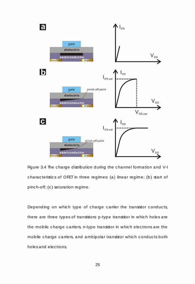
An organic field-effect transistor (OFET) is a three terminal device that is
used to control electric signals through manipulation of an internal
electric field. As in the schematic of an OFET shown in figure 3.3, a typical
OFET consists of three electrodes (drain, source and gate), An organic
semiconductor and a dielectric layer. The “channel” is a conductive
part of the semiconductor layer that accounts for charge transport. A
current (IDS) flows from the source to the drain through the channel. The
gate voltage (VG) controls the electric field that acts to induce charge
carriers into the channel, and hence regulates the conductivity of the
channel.
Figure 3.3 The schematic of an OFET.
The gate/dielectric/semiconductor stack functions as a capacitor, with
the capacitance per area Ci given by
(3.1)
23
where ε0 is the vacuum permittivity, k is relative permittivity and d is the
thickness of the dielectric layer.
When there is no voltage applied between gate and source electrodes,
the transistor is “off” as the intrinsic organic semiconductor usually has a
high electrical resistance. When a voltage is applied at the gate
electrode, the charge carriers accumulate at the interface between the
dielectric and semiconductor layer. The accumulated charge is
proportional to Vg and Ci. However, some of the charges are trapped
and do not contribute to the conduction of the channel. Thus the
effective accumulated charge density Q is given by
(3.2)
where VT is threshold voltage, above which the traps are filled.
When a VG greater than VT is applied, a uniform distribution of charge
carriers is induced, and the transistor is turned on. Under this condition,
the relation between drain-source voltage (VDS) and IDS is detailed as
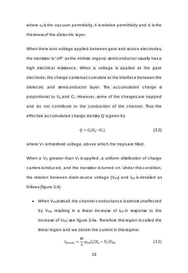
follows (figure 3.4):
When VDS is small, the channel conductance is almost unaffected
by VDS, resulting in a linear increase of IDS in response to the
increase of VDS; see figure 3.4a. Therefore this region is called the
linear region and we obtain the current in this regime:
, 3.2

24
Where is the field-effect mobility in the linear region and W, L
are the width and length of the transistor channel, respectively.
As VDS is further increased, the accumulated charge carriers
adjacent to the drain electrode start to decrease, leading to a
gradual increase of the channel resistance. This is reflected as a
decrease of the slope in the curve of figure 3.4b. When VDS
reaches a point equal to the effective gate voltage (VDS=VG-VT),
a charge depleted region is created. This phenomenon is called
is pinch-off.
A further increase of VDS causes the pinch-off region to grow
towards the source electrode, and a space-charge limited
current flows in this region. Since the potential at the pinch-off
point is equal to VG-VT, the potential drop between the pinch-off
point and source electrode remains constant, resulting in a
constant drain-source current; see figure 3.4c. Thus the transistor
saturates. The saturation current is given by:
, 2 3.3
where is the field-effect mobility in the saturation regime.
25
Figure 3.4 The charge distribution during the channel formation and V-I
characteristics of OFET in three regimes: (a) linear regime; (b) start of
pinch-off; (c) saturation regime.
Depending on which type of charge carrier the transistor conducts,
there are three types of transistors: p-type transistor in which holes are
the mobile charge carriers, n-type transistor in which electrons are the
mobile charge carriers, and ambipolar transistor which conducts both
holes and electrons.
26
3.2.1 SCALING OF TRANSISTORS
Down-scaling of transistors has been a continuous trend since their
invention, as transistors with smaller feature size enable higher packing
density. Moreover, a smaller channel length leads to higher channel
current, as shown in equations (3.2) and (3.3). As the channel shrinks, the
time for a charge carrier to travel between drain and source reduces,
and therefore a transistor switches faster with a shorter L.
As the channel length of transistor is reduced, the lateral electric field
originating from drain and source becomes more significant and starts
to influence the transverse electric field induced by the gate electrode.
As a result, the short-channel transistor characteristics deviate from those
of a long-channel transistor(77-87). This phenomenon is called “short-
channel effect”.
Short channel effects include insufficient saturation(77), threshold
voltage reduction and an increase of drain-source leakage current(88).
The short channel effect can be suppressed by proportional increase of
the transverse electric field induced by the gate electrode(79).
3.2.2 ELECTROLYTE GATED FIELD-EFFECT TRANSISTOR
As equations (3.2) and (3.3) suggest, in order to achieve low-voltage
operation of an OFET, a large Ci is highly desired. Two common
approaches to increase this parameter are utilization of a high-k
dielectric and use of an ultrathin dielectric(89). Alternatively, the
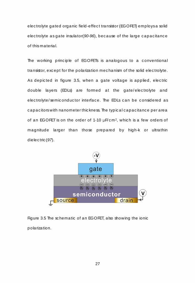
27
electrolyte gated organic field-effect transistor (EGOFET) employs a solid
electrolyte as gate insulator(90-96), because of the large capacitance
of this material.
The working principle of EGOFETs is analogous to a conventional
transistor, except for the polarization mechanism of the solid electrolyte.
As depicted in figure 3.5, when a gate voltage is applied, electric
double layers (EDLs) are formed at the gate/electrolyte and
electrolyte/semiconductor interface. The EDLs can be considered as
capacitors with nanometer thickness. The typical capacitance per area
of an EGOFET is on the order of 1-10 μF/cm2, which is a few orders of
magnitude larger than those prepared by high-k or ultrathin
dielectric(97).
Figure 3.5 The schematic of an EGOFET, also showing the ionic
polarization.
28
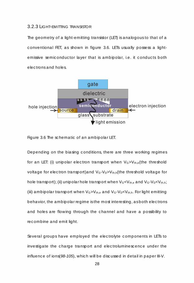
3.2.3 LIGHT-EMITTING TRANSISTOR
The geometry of a light-emitting transistor (LET) is analogous to that of a
conventional FET, as shown in figure 3.6. LETs usually possess a light-
emissive semiconductor layer that is ambipolar, i.e. it conducts both
electrons and holes.
Figure 3.6 The schematic of an ambipolar LET.
Depending on the biasing conditions, there are three working regimes
for an LET: (i) unipolar electron transport when VG>Vth,e(the threshold
voltage for electron transport)and VG-VD>Vth,h(the threshold voltage for
hole transport); (ii) unipolar hole transport when VG<Vth,e and VG-VD<Vth,h;
(iii) ambipolar transport when VG>Vth,e and VG-VD<Vth,h. For light emitting
behavior, the ambipolar regime is the most interesting, as both electrons
and holes are flowing through the channel and have a possibility to
recombine and emit light.
Several groups have employed the electrolyte components in LETs to
investigate the charge transport and electroluminescence under the
influence of ions(98-105), which will be discussed in detail in paper III-V.
29
3.3 P-N JUNCTION DIODES AND CIRCUITS
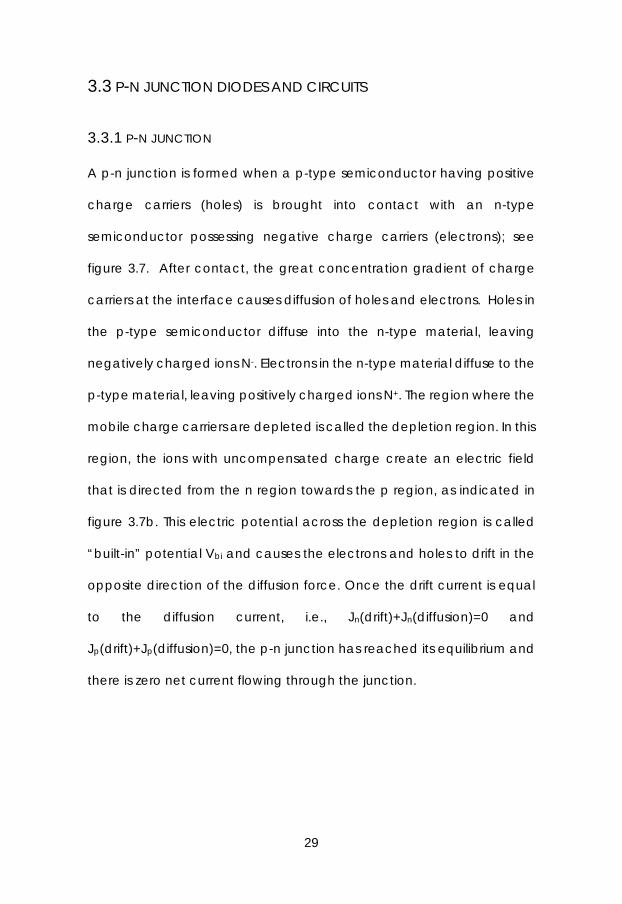
3.3.1 P-N JUNCTION
A p-n junction is formed when a p-type semiconductor having positive
charge carriers (holes) is brought into contact with an n-type
semiconductor possessing negative charge carriers (electrons); see
figure 3.7. After contact, the great concentration gradient of charge
carriers at the interface causes diffusion of holes and electrons. Holes in
the p-type semiconductor diffuse into the n-type material, leaving
negatively charged ions N-. Electrons in the n-type material diffuse to the
p-type material, leaving positively charged ions N+. The region where the
mobile charge carriers are depleted is called the depletion region. In this
region, the ions with uncompensated charge create an electric field
that is directed from the n region towards the p region, as indicated in
figure 3.7b. This electric potential across the depletion region is called
“built-in” potential Vbi and causes the electrons and holes to drift in the
opposite direction of the diffusion force. Once the drift current is equal
to the diffusion current, i.e., Jn(drift)+Jn(diffusion)=0 and
Jp(drift)+Jp(diffusion)=0, the p-n junction has reached its equilibrium and
there is zero net current flowing through the junction.
30
Figure 3.7 (a) p- and n-type semiconductor before they are joined. (b)
The formation and band structure of the p-n junction.
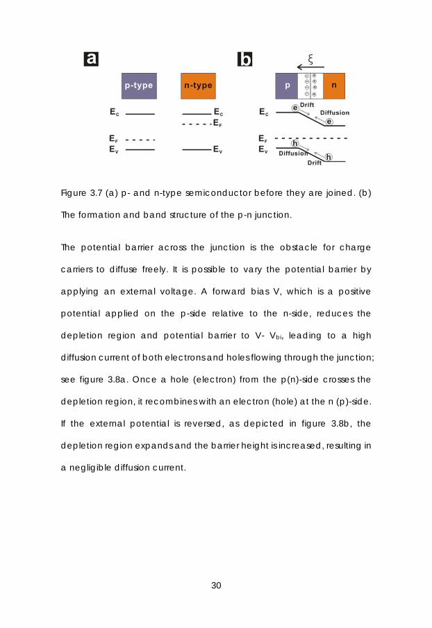
The potential barrier across the junction is the obstacle for charge
carriers to diffuse freely. It is possible to vary the potential barrier by
applying an external voltage. A forward bias V, which is a positive
potential applied on the p-side relative to the n-side, reduces the
depletion region and potential barrier to V- Vbi, leading to a high
diffusion current of both electrons and holes flowing through the junction;
see figure 3.8a. Once a hole (electron) from the p(n)-side crosses the
depletion region, it recombines with an electron (hole) at the n (p)-side.
If the external potential is reversed, as depicted in figure 3.8b, the
depletion region expands and the barrier height is increased, resulting in
a negligible diffusion current.
31
Figure 3.8 Depletion region and band structure for p-n junction under (a)
forward bias and (b) reverse bias.
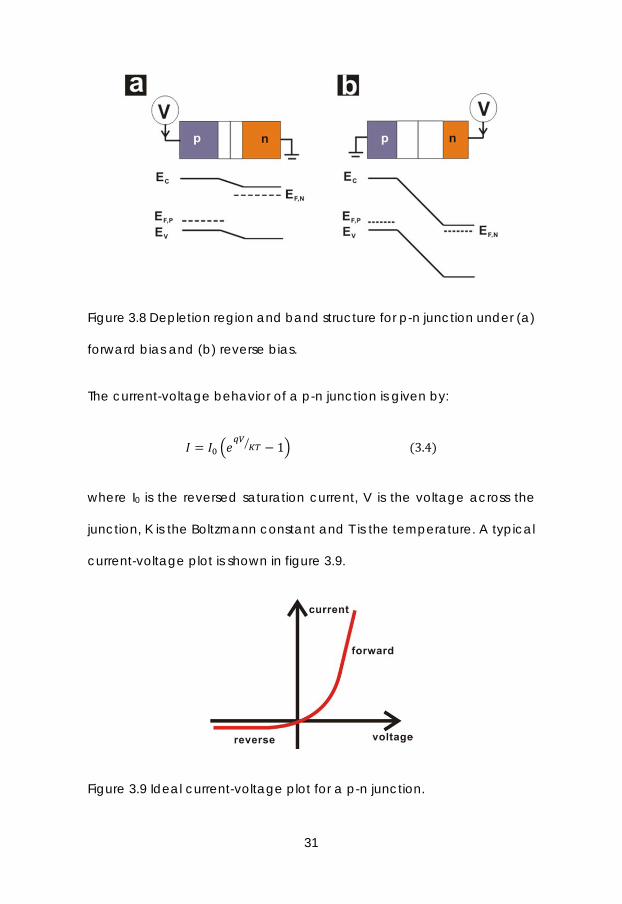
The current-voltage behavior of a p-n junction is given by:
1 3.4
where I0 is the reversed saturation current, V is the voltage across the
junction, K is the Boltzmann constant and T is the temperature. A typical
current-voltage plot is shown in figure 3.9.
Figure 3.9 Ideal current-voltage plot for a p-n junction.

32
3.3.2 CIRCUITS BASED ON P-N DIODES
A p–n diode is a two-terminal electric component based upon the p–n
junction. The p side is termed anode and the n side is the cathode,
corresponding to the circuit diagram symbol displayed in figure 3.10. The
diode conducts when the anode is positively biased with respect to the
cathode, and becomes an isolator when the bias is reversed. This so-
called “rectification” property makes diodes useful in circuit construction.
Figure 3.10 The symbol of a p-n diode.
Using diodes, it is possible to construct diode-resistor logics, which is
Boolean logic gates composed of a diode and resistor network.
Although these logic gates can be made with high simplicity, only non-
inverted Boolean logic (AND gate and OR gate) can be constructed. To
achieve inverted logic (NOT, NAND, NOR etc.), a diode-transistor
network must be used.
The diode-resistor circuits for OR and AND gates are shown in figure 3.11.
To understand how these circuits work, we assume that a diode is a
resistor with zero resistance when forward biased, and infinite resistance
when reverse biased. In an OR gate, if any of the voltage inputs is high
33
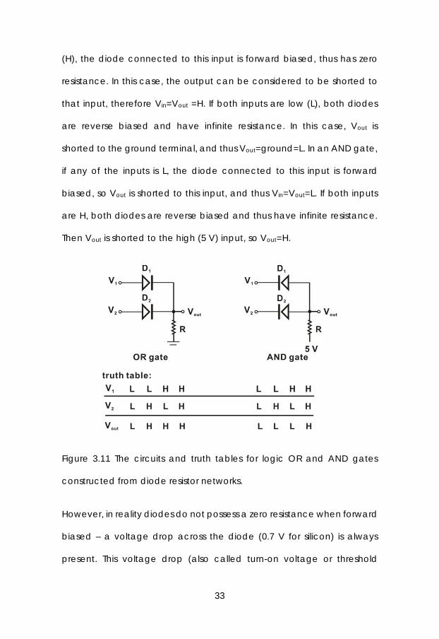
(H), the diode connected to this input is forward biased, thus has zero
resistance. In this case, the output can be considered to be shorted to
that input, therefore Vin=Vout =H. If both inputs are low (L), both diodes
are reverse biased and have infinite resistance. In this case, Vout is
shorted to the ground terminal, and thus Vout=ground=L. In an AND gate,
if any of the inputs is L, the diode connected to this input is forward
biased, so Vout is shorted to this input, and thus Vin=Vout=L. If both inputs
are H, both diodes are reverse biased and thus have infinite resistance.
Then Vout is shorted to the high (5 V) input, so Vout=H.
Figure 3.11 The circuits and truth tables for logic OR and AND gates
constructed from diode resistor networks.
However, in reality diodes do not possess a zero resistance when forward
biased – a voltage drop across the diode (0.7 V for silicon) is always
present. This voltage drop (also called turn-on voltage or threshold
34
voltage, denoted VT) leads to a voltage loss for each stage of diode
logic. Take the OR gate for example, when the two inputs are H (5 V)
and L (0 V), the resulting output would be H (4.3 V), instead of H (5 V) in
an ideal case. The voltage loss is more significant when cascading
several diode logic gates. As a result, diode logic is only used in single
stage logic applications due to the lack of voltage amplification at
each stage.
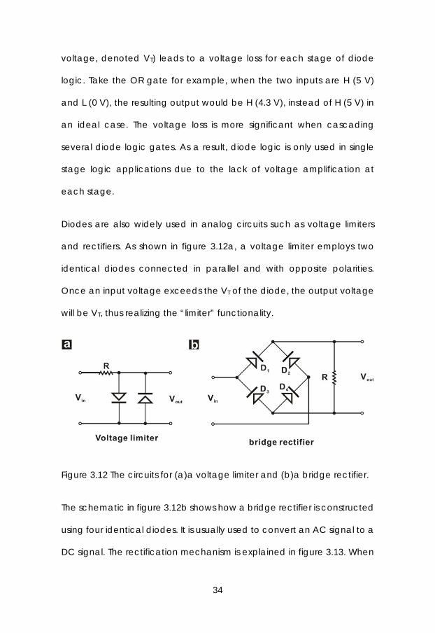
Diodes are also widely used in analog circuits such as voltage limiters
and rectifiers. As shown in figure 3.12a, a voltage limiter employs two
identical diodes connected in parallel and with opposite polarities.
Once an input voltage exceeds the VT of the diode, the output voltage
will be VT, thus realizing the “limiter” functionality.
Figure 3.12 The circuits for (a)a voltage limiter and (b)a bridge rectifier.
The schematic in figure 3.12b shows how a bridge rectifier is constructed
using four identical diodes. It is usually used to convert an AC signal to a
DC signal. The rectification mechanism is explained in figure 3.13. When

35
the input is a positive voltage, diodes D2 and D3 are forward biased and
function as resistors with 0.7 V voltage drop; diodes D1 and D4 are reverse
biased and thus function as resistors with infinite resistance that are
ineffective in the circuit. In this case, as the effective circuit in figure 3.13a
shows, the output voltage equals the voltage drop over R, which is the
input voltage subtracted by the voltage drop on D2 and D3. Therefore
we obtain Vout=Vin-2VT when Vin>0. Similarly, when a negative voltage is
applied, the effective circuit is shown in 3.13b and the output voltage is
given by: Vout=-Vin-2VT when Vin<0. In summary, we obtain Vout=|Vin|-2VT
for input voltages of either polarity.
Figure 3.13 effective circuit for a diode bridge when the input voltage is
(a) positive and (b) negative.

36

37
Chapter 4. Fabrication and Characterization
Manufacturing methods commonly used for organic electronics were
utilized for the devices in this thesis. In this chapter, an overview of these
methods is given, together with a short description of the electrical
characterization methods employed.
4.1 DEVICE FABRICATION
The fabrication was performed in a cleanroom (class 1 000-10 000). All
the manufacturing processes were carried out in ambient atmosphere if
not mentioned otherwise. All the devices/circuits were constructed on
silicon wafers with a thermally grown oxide (1 µm thick).
4.1.1 DEPOSITION AND PATTERNING OF METAL ELECTRODES
To fabricate electrodes with spacing higher than 400 µm, thermal
evaporation in vacuum through a shadow-mask was performed. The
plastic shadow mask was made in a plotter machine (Graphtec FC

38
2200-90Ex). This technique is very powerful for user-customization since
the turnaround time is only about one day.
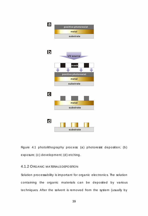
To manufacture electrodes with spacing smaller than 400 µm,
photolithography is performed in the following steps (figure 4.1): (a) After
a global layer of metal is evaporated onto the substrate, a layer of
positive photoresist is deposited and cured; (b) UV exposure is performed
through a photo mask; (c) the exposed photoresist is dissolved in a
developer, while the unexposed photoresist remains intact in the
developer and serves as the protection layer in the following etching
process; (d) finally the etching agent dissolves the uncovered metal,
leaving the remainder of metal in the desired pattern. Photolithography
offers high precision in materials patterning; however, in project planning
one needs to take into account that the turnaround time for ordering a
photolithographic mask from an external party usually varies from one
week to one month.
39
Figure 4.1 photolithography process: (a) photoresist deposition; (b)
exposure; (c) development; (d) etching.
4.1.2 ORGANIC MATERIALS DEPOSITION
Solution processability is important for organic electronics. The solution
containing the organic materials can be deposited by various
techniques. After the solvent is removed from the system (usually by

40
heating), the organic materials become solidified. The most common
techniques used in this thesis are spin-coating and drop-casting.
In the spin-coating process, the substrate is covered by the solution and
is rotated to spread the materials by centrifugal force. As the solvent
evaporates during and after the spinning, a homogeneous film results.
The thickness of the film is determined by the spinning speed, spinning
duration and solution properties (e.g., surface wettability, materials
concentration and evaporation rate of the solvent).
Drop-casting is widely used in the work covered in this thesis, due to its
simplicity and versatility. A drop of solution containing the active
compound was placed onto the substrate and subsequently dried.
Drop-casting can be applied to any substrate and is not restricted to
surface roughness and wetting compatibility. The resulting film is usually
thicker and less uniform than one prepared by spin-coating.
4.2 CHARACTERIZATION
All the characterization in this thesis except the EGOFET measurement
was carried out under vacuum in a cryogenic station; see figure 4.2a. As
the sketch displayed in figure 4.2b shows, the cryogenic station is
equipped with a sample platen with heating/cooling function, four
probe manipulators, and an optical window through which images can
be recorded using a camera and a microscope. The external UV source

41
is used to excite the polymer sample in order to induce
photoluminescence.
All the electrical measurements were performed by means of a Keithley
4200 Semiconductor Parameter Analyzer. The Keithley 4200 possesses
multiple measurement units, each of which can source a current (or
voltage) and measure the voltage (or current) at the same time.
Figure 4.2 (a) Photograph and (b) sketch of the cryogenic station.

42
43
Chapter 5. Summary of the Manuscripts
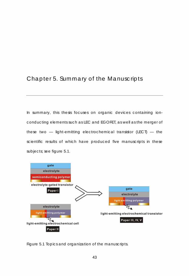
In summary, this thesis focuses on organic devices containing ion-
conducting elements such as LEC and EGOFET, as well as the merger of
these two — light-emitting electrochemical transistor (LECT) — the
scientific results of which have produced five manuscripts in these
subjects; see figure 5.1.
Figure 5.1 Topics and organization of the manuscripts.

44
In paper I, we develop an EGOFET having a vertical drain-source
structure with a short channel. The fabrication merely requires a low-
resolution and mask-free photolithography process. We have
demonstrated short-channel transistors with 2.2 and 0.7 µm channel
length, which are operational below 1 V and show clear saturation.
Vertical EGOFET is promising for large-area, low-voltage circuits with
simple fabrication steps.
In paper II, we take advantage of the reversible electrochemical doping
of LECs, to develop printable and reconfigurable logic circuits. We
constructed an LEC array where several p-n diodes can be
simultaneously formed with desired polarity at different locations, thus
enabling the creation of various circuits based on this diode-network.
Any circuit made can be erased by heating, and turned into another
circuit with different functionality by electrically forming diodes in other
patterns. For example, the diodes of an AND gate can be
reprogrammed to form an OR gate.
In paper III, a device that combines a transistor and an LEC is developed:
LECT. We employ an ion-conductive gate made from PEDOT:PSS onto a
conventional bilayer LEC, and use it to modify the doping level of the
electrochemical p- and n-doping. Through proper control from the gate,
we can turn on the LECT already at a voltage below 4 V, and move the
emission zone back and forth within a 500 µm channel. This device also
45
displays a clear transistor behavior: it has an on/off ratio about 50, a gate
threshold voltage of -2.3 V and a transconductance value of about 2 µS.
In paper IV, we aim to improve the control of the LECT presented in
paper III. To do so, we utilize two gate terminals on the LEC, with one
controlling the p-doping and another the n-doping. The location of the
light emission zone can be precisely defined, as it aligns with the area
that is not covered by any gate. We demonstrate double-gate LECTs
with two different gate patterns, showing a homogeneously centered
emission zone as well as a zigzag one. We also propose an electrical
model to explain the gate-doping process. The double-gate LECT is
designed to combat the off-centered emission zone in LEC, which is
detrimental in device efficiency.
In paper V, we demonstrate a simplified version of the double-gate LECT
from paper IV, by omitting the gate terminal that is responsible for p-
doping. Having only one gate terminal covering the n-doping region,
this device also displays a centered emissive p-n junction, in a similar
manner as the double-gate LECT, because the p-doping is by nature
more active than n-doping. Moreover, we prove that this half-gate LECT
outperforms the corresponding LEC in efficiency, due to a more
centered emission zone. We also calculate the doping level of the
semiconductor material in the LECT, and conclude that it reaches a level
that is comparable to a conventional LEC.

46
47
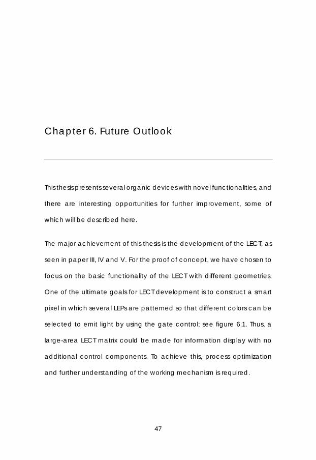
Chapter 6. Future Outlook
This thesis presents several organic devices with novel functionalities, and
there are interesting opportunities for further improvement, some of
which will be described here.
The major achievement of this thesis is the development of the LECT, as
seen in paper III, IV and V. For the proof of concept, we have chosen to
focus on the basic functionality of the LECT with different geometries.
One of the ultimate goals for LECT development is to construct a smart
pixel in which several LEPs are patterned so that different colors can be
selected to emit light by using the gate control; see figure 6.1. Thus, a
large-area LECT matrix could be made for information display with no
additional control components. To achieve this, process optimization
and further understanding of the working mechanism is required.

48
Figure 6.1 A smart pixel that can be made from LECT.
First of all, control of the emissive zone should be more reproducible and
predictable, which necessitates a more homogeneous polymer film. We
have used coarse drop-casting to deposit electrolyte layers with high
roughness. In a refined device, this can be replaced by other thin-film
coating methods such as inkjet printing or slot-die coating, to achieve
higher uniformity of the polymer film.
Secondly, the lifetime of the device needs to be greatly increased. The
short lifetime is attributed to the presence of water and oxygen, which
deteriorates the LEP during n-doping, and the side reaction between the
ion-conducting polymer (such as PEO) and the exciton. The ultimate
solution for the lifetime issue requires advancement of the materials
science: to design an LEP that is inert to oxygen or water upon both p-
and n-doping, and a polymer electrolyte with a broad stability window
to eliminate the side reaction.
Last but not least, better understanding of the working mechanism is
necessary. In paper III we propose an electrical model corresponding to
device resistance of the LECT, which varies with time as the doping

49
progresses. However, the resistance through the device is not
homogenous. A resistance mapping with high resolution is strongly
desired to study the doping level progression for both p- and n-doping,
as well as the doping level to resistance relation. This measurement can
be done, for example, by four-probe resistance measurement with a
moving stage or a probe array.
As for reconfigurable circuits based on LEC mentioned in paper II, we
have demonstrated several simple digital and analog circuits made
from the LEC array, and it opens a route to facilitate more complex
systems based on the same concept. To realize a system bearing more
functionality, one needs to integrate other electronic components that
can be made from the same materials. The LEC is made by intermixing
or stacking an LEP and an electrolyte. With these two core materials,
many other electronic components can be made. An undoped LEP is a
resistor; an electrolyte can be made into a capacitor; the LEC is a resistor
with tunable resistance, depending on the doping level; an LEC can be
turned into a transistor with addition of a gate terminal; LECs also show
photovoltaic behavior when charged and frozen. All these multiple
functionalities can be achieved by simple fabrication. Together with the
circuit design that was demonstrated in paper II, a system with easy
integration and fabrication should be achievable. Furthermore, the
reconfigurable circuits require a low temperature to immobilize the ions
due to the low glass transition temperature (-67 °C) of PEO. Utilizing an
50
ion conductor with a high glass transition temperature would allow for
the formation of the frozen junction at room temperature (RT)(68, 74). If
such a material system is adopted, the reconfigurable circuit will be able
to function at RT.

51
References
1. G. E. Moore. Cramming More Components Onto Integrated Circuits. Proceedings of the IEEE 86, 82 (1998).
2. H. Shirakawa, E. J. Louis, A. G. Macdiarmid, C. K. Chiang, A. J. Heeger. Synthesis of Electrically Conducting Organic Polymers - Halogen Derivatives of Polyacetylene, (Ch)X. Journal of the Chemical Society-Chemical Communications, 578 (1977).
3. O. G. Piringer, A. L. Baner, Plastic packaging: interactions with food and pharmaceuticals. (Wiley. com, 2008).
4. R. V. Kasowski, W. Y. Hsu, E. B. Caruthers. Electronic properties of polyacetylene, polyethylene, and polytetrafluoroethylene. The Journal of Chemical Physics 72, 4896 (1980).
5. U. Salzner, J. B. Lagowski, P. G. Pickup, R. A. Poirier. Comparison of geometries and electronic structures of polyacetylene, polyborole, polycyclopentadiene, polypyrrole, polyfuran, polysilole, polyphosphole, polythiophene, polyselenophene and polytellurophene. Synthetic Metals 96, 177 (8/15/, 1998).
6. R. Friend, R. Gymer, A. Holmes, J. Burroughes, R. Marks, C. Taliani, D. Bradley, D. Dos Santos, J. Bredas, M. Lögdlund. Electroluminescence in conjugated polymers. Nature 397, 121 (1999).
7. D. Fenton, J. Parker, P. Wright. Complexes of alkali metal ions with poly (ethylene oxide). Polymer 14, 589 (1973).
8. L. Dai, Intelligent macromolecules for smart devices: from materials synthesis to device applications. (Springer, 2004).
9. D. Brandell, Understanding ionic conductivity in crystalline polymer electrolytes, Uppsala University (2005).
10. J. Cowie, S. Cree. Electrolytes dissolved in polymers. Annual Review of Physical Chemistry 40, 85 (1989).
11. F. M. Gray, Solid polymer electrolytes. (VCH New Tork etc., 1991). 12. W. H. Meyer. Polymer Electrolytes for Lithium-Ion Batteries. Advanced
Materials 10, 439 (1998).
52
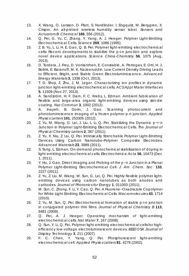
13. X. Wang, O. Larsson, D. Platt, S. Nordlinder, I. Engquist, M. Berggren, X. Crispin. An all-printed wireless humidity sensor label. Sensors and Actuators B: Chemical 166, 556 (2012).
14. Q. Pei, G. Yu, C. Zhang, Y. Yang, A. J. Heeger. Polymer Light-Emitting Electrochemical Cells. Science 269, 1086 (1995).
15. Z. B. Yu, L. Li, H. E. Gao, Q. B. Pei. Polymer light-emitting electrochemical cells: Recent developments to stabilize the p-i-n junction and explore novel device applications. Science China-Chemistry 56, 1075 (Aug, 2013).
16. D. Tordera, J. Frey, D. Vonlanthen, E. Constable, A. Pertegas, E. Orti, H. J. Bolink, E. Baranoff, M. K. Nazeeruddin. Low Current Density Driving Leads to Efficient, Bright, and Stable Green Electroluminescence. Advanced Energy Materials 3, 1338 (Oct, 2013).
17. T. D. Shoji, Z. Zhu, J. M. Leger. Characterizing ion profiles in dynamic junction light-emitting electrochemical cells. ACS Appl Mater Interfaces 5, 11509 (Nov 27, 2013).
18. A. Sandström, H. F. Dam, F. C. Krebs, L. Edman. Ambient fabrication of flexible and large-area organic light-emitting devices using slot-die coating. Nat Commun 3, 1002 (2012).
19. A. Inayeh, B. Dorin, J. Gao. Scanning photocurrent and photoluminescence imaging of a frozen polymer p-n junction. Applied Physics Letters 101, 253305 (2012).
20. Z. Yu, M. Wang, G. Lei, J. Liu, L. Li, Q. Pei. Stabilizing the Dynamic p−i−n Junction in Polymer Light-Emitting Electrochemical Cells. The Journal of Physical Chemistry Letters 2, 367 (2011).
21. Z. Yu, X. Niu, Z. Liu, Q. Pei. Intrinsically Stretchable Polymer Light-Emitting Devices Using Carbon Nanotube-Polymer Composite Electrodes. Advanced Materials 23, 3989 (2011).
22. S. Tang, L. Edman. On-demand photochemical stabilization of doping in light-emitting electrochemical cells. Electrochimica Acta 56, 10473 (Dec 1, 2011).
23. Y. Hu, J. Gao. Direct Imaging and Probing of the p−n Junction in a Planar Polymer Light-Emitting Electrochemical Cell. J. Am. Chem. Soc. 133, 2227 (2011).
24. Z. Yu, Z. Liu, M. Wang, M. Sun, G. Lei, Q. Pei. Highly flexible polymer light-emitting devices using carbon nanotubes as both anodes and cathodes. Journal of Photonics for Energy 1, 011003 (2011).
25. M. Sun, C. Zhong, F. Li, Y. Cao, Q. Pei. A Fluorene−Oxadiazole Copolymer for White Light-Emitting Electrochemical Cells. Macromolecules 43, 1714 (2010).
26. Z. Yu, M. Sun, Q. Pei. Electrochemical formation of stable p-i-n junction in conjugated polymer thin films. Journal of Physical Chemistry B 113, 8481 (2009).
27. Q. Pei, A. J. Heeger. Operating mechanism of light-emitting electrochemical cells. Nat Mater 7, 167 (2008).
28. Q. Sun, Y. Li, Q. Pei. Polymer light-emitting electrochemical cells for high-efficiency low-voltage electroluminescent devices. IEEE/OSA Journal of Display Technology 3, 211 (2007).
29. F. C. Chen, Y. Yang, Q. Pei. Phosphorescent light-emitting electrochemical cell. Applied Physics Letters 81, 4278 (2002).

53
30. Y. Yang, Q. Pei. Light-emitting electrochemical cells from a blend of p- and n-type luminescent conjugated polymers. Applied Physics Letters 70, 1926 (1997).
31. Q. Pei, Y. Yang, G. Yu, Y. Cao, A. J. Heeger. Solid state polymer light-emitting electrochemical cells: Recent developments. Synthetic Metals 85, 1229 (1997).
32. Y. Cao, Q. Pei, M. R. Andersson, G. Yu, A. J. Heeger. Light-emitting electrochemical cells with crown ether as solid electrolyte. Journal of the Electrochemical Society 144, (1997).
33. Y. Yang, Q. Pei. Voltage controlled two color light-emitting electrochemical cells. Applied Physics Letters 68, 2708 (1996).
34. Q. Pei, Y. Yang, G. Yu, C. Zhang, A. J. Heeger. Polymer light-emitting electrochemical cells: In situ formation of a light-emitting p-n junction. Journal of the American Chemical Society 118, 3922 (1996).
35. Q. Pei, Y. Yang. Solid-state polymer light-emitting electrochemical cells. Synthetic Metals 80, 131 (1996).
36. S. Tang, W. Y. Tan, X. H. Zhu, L. Edman. Small-molecule light-emitting electrochemical cells: evidence for in situ electrochemical doping and functional operation. Chem Commun (Camb) 49, 4926 (May 28, 2013).
37. S. Tang, J. Pan, H. A. Buchholz, L. Edman. White light from a single-emitter light-emitting electrochemical cell. J Am Chem Soc 135, 3647 (Mar 6, 2013).
38. S. Tang, A. Sandström, J. Fang, L. Edman. A Solution-Processed Trilayer Electrochemical Device: Localizing the Light Emission for Optimized Performance. Journal of the American Chemical Society 134, 14050 (2012/08/29, 2012).
39. N. D. Robinson, L. Edman, M. Chhowalla. Graphene electrodes for organic metal-free light-emitting devices. Physica Scripta 2012, 014023 (2012).
40. A. Munar, A. Sandstrom, S. Tang, L. Edman. Shedding Light on the Operation of Polymer Light-Emitting Electrochemical Cells Using Impedance Spectroscopy. Advanced Functional Materials 22, 1511 (Apr 10, 2012).
41. A. Asadpoordarvish, A. Sandström, S. Tang, J. Granström, L. Edman. Encapsulating light-emitting electrochemical cells for improved performance. Applied Physics Letters 100, 193508 (May 7, 2012).
42. S. van Reenen, P. Matyba, A. Dzwilewski, R. A. J. Janssen, L. Edman, M. Kemerink. Salt Concentration Effects in Planar Light-Emitting Electrochemical Cells. Adv. Funct. Mater. 21, 1795 (2011).
43. S. Tang, J. Pan, H. Buchholz, L. Edman. White Light-Emitting Electrochemical Cell. ACS Applied Materials & Interfaces 3, 3384 (2011/09/28, 2011).
44. V. Bychkov, P. Matyba, V. Akkerman, M. Modestov, D. Valiev, G. Brodin, C. K. Law, M. Marklund, L. Edman. Speedup of Doping Fronts in Organic Semiconductors through Plasma Instability. Physical Review Letters 107, 016103 (2011).
45. S. van Reenen, P. Matyba, A. Dzwilewski, R. A. Janssen, L. Edman, M. Kemerink. A unifying model for the operation of light-emitting electrochemical cells. J Am Chem Soc 132, 13776 (Oct 6, 2010).
46. S. Tang, K. Irgum, L. Edman. Chemical stabilization of doping in conjugated polymers. Organic Electronics 11, 1079 (2010).
54
47. S. Tang, L. Edman. Quest for an Appropriate Electrolyte for High-Performance Light-Emitting Electrochemical Cells. The Journal of Physical Chemistry Letters 1, 2727 (2010).
48. A. Sandstrom, P. Matyba, O. Inganas, L. Edman. Separating Ion and Electron Transport: The Bilayer Light-Emitting Electrochemical Cell. Journal of the American Chemical Society 132, 6646 (2010/05/19, 2010).
49. P. Matyba, K. Maturova, M. Kemerink, N. D. Robinson, L. Edman. The dynamic organic p-n junction. Nature. Mater. 8, 672 (2009).
50. J. D. Slinker, J. A. DeFranco, M. J. Jaquith, W. R. Silveira, Y. W. Zhong, J. M. Moran-Mirabal, H. G. Craighead, H. D. Abrũa, J. A. Marohn, G. G. Malliaras. Direct measurement of the electric-field distribution in a light-emitting electrochemical cell. Nature. Mat. 6, 894 (2007).
51. L. S. C. Pingree, D. B. Rodovsky, D. C. Coffey, G. P. Bartholomew, D. S. Ginger. Scanning Kelvin Probe Imaging of the Potential Profiles in Fixed and Dynamic Planar LECs. Journal of the American Chemical Society 129, 15903 (2007).
52. D. B. Rodovsky, O. G. Reid, L. S. C. Pingree, D. S. Ginger. Concerted Emission and Local Potentiometry of Light-Emitting Electrochemical Cells. ACS Nano 4, 2673 (2010).
53. Y. Hu, Y. Zhang, J. Gao. Strong Electroluminescence from Polymer Films with Heavily Quenched Photoluminescence. Advanced Materials 18, 2880 (2006).
54. Y. Hu, C. Tracy, J. Gao. High-resolution imaging of electrochemical doping and dedoping processes in luminescent conjugated polymers. Applied Physics Letters 88, 123507 (2006).
55. Y. Hu, J. Gao. Direct Probing of a Polymer Electrolyte/Luminescent Conjugated Polymer Mixed Ionic/Electronic Conductor. Journal of the American Chemical Society 131, 18236 (2009).
56. J. Gao, J. Dane. Visualization of electrochemical doping and light-emitting junction formation in conjugated polymer films. Applied Physics Letters 84, 2778 (2004).
57. J. Gao, J. Dane. Imaging the doping and electroluminescence in extremely large planar polymer light-emitting electrochemical cells. Journal of Applied Physics 98, 1 (2005).
58. D. J. Dick, A. J. Heeger, Y. Yang, Q. Pei. Imaging the structure of the p-n junction in polymer light-emitting electrochemical cells. Advanced Materials 8, 985 (1996).
59. J. Shin, P. Matyba, N. Robinson, L. Edman. The influence of electrodes on the performance of light-emitting electrochemical cells. Electrochimica Acta 52, 6456 (2007).
60. D. Hohertz, J. Gao. How electrode work function affects doping and electroluminescence of polymer light-emitting electrochemical cells. Advanced Materials 20, 3298 (2008).
61. P. Matyba, H. Yamaguchi, G. Eda, M. Chhowalla, L. Edman, N. D. Robinson. Graphene and Mobile Ions: The Key to All-Plastic, Solution-Processed Light-Emitting Devices. ACS Nano 4, 637 (2010).
62. Q. Sun, C. Yang, G. He, Y. Li, H. Wang. Effects of electrode modifications on the performance of polymer light-emitting electrochemical cells. Synthetic Metals 138, 561 (2003).
55
63. H. L. Filiatrault, G. C. Porteous, R. S. Carmichael, G. J. E. Davidson, T. B. Carmichael. Stretchable Light-Emitting Electrochemical Cells Using an Elastomeric Emissive Material. Advanced Materials 24, 2673 (2012).
64. T. Wågberg, P. R. Hania, N. D. Robinson, J. H. Shin, P. Matyba, L. Edman. On the limited operational lifetime of light-emitting electrochemical cells. Advanced Materials 20, 1744 (2008).
65. J. Fang, P. Matyba, N. D. Robinson, L. Edman. Identifying and alleviating electrochemical side-reactions in light-emitting electrochemical cells. J. Am. Chem. Soc. 130, 4562 (2008).
66. J. Gao, G. Yu, A. J. Heeger. Polymer light-emitting electrochemical cells with frozen p-i-n junction. Applied Physics Letters 71, 1293 (1997).
67. L. Yongfang, J. Gao, D. Wang, Y. Gang, Y. Cao, A. J. Heeger. A.c. impedance of frozen junction polymer light-emitting electrochemical cells. Synthetic Metals 97, 191 (1998).
68. G. Yu, Y. Cao, M. Andersson, J. Gao, A. J. Heeger. Polymer Light-Emitting Electrochemical Cells with Frozen p-i-n Junction at Room Temperature. Advanced Materials 10, 385 (1998).
69. J. Gao, Y. Li, G. Yu, A. J. Heeger. Polymer light-emitting electrochemical cells with frozen junctions. Journal of Applied Physics 86, 4594 (10/15/, 1999).
70. C. Yang, Q. Sun, J. Qiao, Y. Li. Ionic Liquid Doped Polymer Light-Emitting Electrochemical Cells. The Journal of Physical Chemistry B 107, 12981 (2003/11/01, 2003).
71. L. Edman, M. Pauchard, D. Moses, A. J. Heeger. Planar polymer light-emitting device with fast kinetics at a low voltage. Journal of Applied Physics 95, 4357 (2004).
72. J. Dane, C. Tracy, J. Gao. Direct observation of a frozen junction in polymer light-emitting electrochemical cells. Applied Physics Letters 86, 1 (2005).
73. J. H. Shin, S. Xiao, Å. Fransson, L. Edman. Polymer light-emitting electrochemical cells: Frozen-junction operation of an "ionic liquid" device. Applied Physics Letters 87, 1 (2005).
74. G. Wantz, B. Gautier, F. Dumur, T. N. T. Phan, D. Gigmes, L. Hirsch, J. Gao. Towards frozen organic PN junctions at room temperature using high-Tg polymeric electrolytes. Organic Electronics 13, 1859 (2012).
75. I. V. Kosilkin, M. S. Martens, M. P. Murphy, J. M. Leger. Polymerizable Ionic Liquids for Fixed-Junction Polymer Light-Emitting Electrochemical Cells. Chemistry of Materials 22, 4838 (2010/09/14, 2010).
76. J. M. Leger, D. B. Rodovsky, G. P. Bartholomew. Self-Assembled, Chemically Fixed Homojunctions in Semiconducting Polymers. Advanced Materials 18, 3130 (2006).
77. Y. Chen, I. Shih. Scaling down of organic thin film transistors: short channel effects and channel length-dependent field effect mobility. Journal of Materials Science 44, 280 (2009).
78. Y. Cao, M. Steigerwald, C. Nuckolls, X. Guo. Current Trends in Shrinking the Channel Length of Organic Transistors Down to the Nanoscale. Adv. Mater 21, 1 (2009).
79. L. Herlogsson, Y. Noh, N. Zhao, X. Crispin, H. Sirringhaus, M. Berggren. Downscaling of Organic Field-Effect Transistors with a Polyelectrolyte Gate Insulator Advanced Materials 20, (2008).
56
80. L. Bürgi, R. Pfeiffer, C. Winnewisser. Submicrometer polymer transistors fabricated by a mask-free photolithographic self-alignment process. Applied Physics Letters 92, 153302 (2008).
81. N. Zhao, M. Chiesa, H. Sirringhaus, Y. Li, Y. Wu, B. Ong. Self-aligned inkjet printing of highly conducting gold electrodes with submicron resolution. Journal of Applied Physics 101, 064513 (2007).
82. B. Stadlober, U. Haas, H. Gold, A. Haase, G. Jakopic, G. Leising, N. Koch, S. Rentenberger, E. Zojer. Orders-of-Magnitude Reduction of the Contact Resistance in Short-Channel Hot Embossed Organic Thin Film Transistors by Oxidative Treatment of Au-Electrodes This work was supported from the European Commission as part of the POLYAPPLY project (IP507143) and by the Austrian Fonds zur Forderung der Wissenschaftlichen Forschung (P17068-N02). Advanced Functional Materials 17, (2007).
83. S. Ko, H. Pan, C. Grigoropoulos, C. Luscombe, J. Fréchet, D. Poulikakos. Air stable high resolution organic transistors by selective laser sintering of ink-jet printed metal nanoparticles. Applied Physics Letters 90, 141103 (2007).
84. J. Haddock, X. Zhang, S. Zheng, Q. Zhang, S. Marder, B. Kippelen. A comprehensive study of short channel effects in organic field-effect transistors. Organic Electronics 7, 45 (2006).
85. J. Lee, P. Chang, J. Liddle, V. Subramanian. 10-nm channel length pentacene transistors. IEEE Transactions on Electron Devices 52, 1874 (2005).
86. L. Wang, D. Fine, T. Jung, D. Basu, H. von Seggern, A. Dodabalapur. Pentacene field-effect transistors with sub-10-nm channel lengths. Applied Physics Letters 85, 1772 (2004).
87. J. Collet, O. Tharaud, A. Chapoton, D. Vuillaume. Low-voltage, 30 nm channel length, organic transistors with a self-assembled monolayer as gate insulating films. Applied Physics Letters 76, 1941 (2000).
88. S. Sze, Semiconductor devices. (World Scientific, 1991). 89. A. Facchetti, M. H. Yoon, T. J. Marks. Gate Dielectrics for Organic Field-
Effect Transistors: New Opportunities for Organic Electronics. Advanced Materials 17, 1705 (2005).
90. J. H. Cho, J. Lee, Y. Xia, B. S. Kim, Y. He, M. J. Renn, T. P. Lodge, C. D. Frisbie. Printable ion-gel gate dielectrics for low-voltage polymer thin-film transistors on plastic. Nature Mater 7, 900 (2008).
91. L. Herlogsson, X. Crispin, N. D. Robinson, M. Sandberg, O.-J. Hagel, G. Gustafsson, M. Berggren. Low-Voltage Polymer Field-Effect Transistors Gated via a Proton Conductor*. Adv. Mater 19, 97 (2007).
92. E. Said, X. Crispin, L. Herlogsson, S. Elhag, N. D. Robinson, M. Berggren. Polymer field-effect transistor gated via a poly(styrenesulfonic acid) thin film. Applied Physics Letters 89, 143507 (2006).
93. B. Pal, B. Dhar, K. See, H. Katz. Solution-deposited sodium beta-alumina gate dielectrics for low-voltage and transparent field-effect transistors. Nature Materials 8, 898 (2009).
94. S. Ono, K. Miwa, S. Seki, J. Takeya. High-performance organic field-effect transistors with binary ionic liquids. Organic Electronics 10, 1579 (2009).
95. J. Liu, L. Herlogsson, A. Sawatdee, P. Favia, M. Sandberg, X. Crispin, I. Engquist, M. Berggren. Vertical polyelectrolyte-gated organic field-effect transistors. Applied Physics Letters 97, 103303 (2010).

57
96. L. Kergoat, L. Herlogsson, D. Braga, B. Piro, M. C. Pham, X. Crispin, M. Berggren, G. Horowitz. A Water‐Gate Organic Field‐Effect Transistor. Advanced Materials 22, 2565 (2010).
97. S. H. Kim, K. Hong, W. Xie, K. H. Lee, S. Zhang, T. P. Lodge, C. D. Frisbie. Electrolyte-Gated Transistors for Organic and Printed Electronics. Advanced Materials 25, 1822 (2013).
98. Y. Zhou, S. T. Han, G. J. Zhou, W. Y. Wong, V. A. L. Roy. Ambipolar organic light-emitting electrochemical transistor based on a heteroleptic charged iridium(III) complex. Applied Physics Letters 102, 083301 (Feb 25, 2013).
99. C. Yumusak, M. Abbas, N. S. Sariciftci. Optical and electrical properties of electrochemically doped organic field effect transistors. J Lumin 134, 107 (Feb, 2013).
100. J. Liu, I. Engquist, M. Berggren. Double-Gate Light-Emitting Electrochemical Transistor: Confining the Organic p–n Junction. Journal of the American Chemical Society 135, 12224 (2013).
101. S. N. Bhat, R. D. Pietro, H. Sirringhaus. Electroluminescence in Ion-Gel Gated Conjugated Polymer Field-Effect Transistors. Chemistry of Materials, (2012).
102. J. Liu, I. Engquist, X. Crispin, M. Berggren. Spatial Control of p–n Junction in an Organic Light-Emitting Electrochemical Transistor. Journal of the American Chemical Society 134, 901 (2012/01/18, 2011).
103. C. Yumusak, N. S. Sariciftci. Organic electrochemical light emitting field effect transistors. Applied Physics Letters 97, 033302 (2010).
104. A. Hepp, H. Heil, R. Schmechel, H. von Seggern. Electrochemical Interface Doping in Organic Light Emitting Field Effect Transistors. Advanced Engineering Materials 7, 957 (2005).
105. L. Edman, J. Swensen, D. Moses, A. J. Heeger. Toward improved and tunable polymer field-effect transistors. Applied Physics Letters 84, 3744 (2004).

58

59
The Papers

60

Papers
The articles associated with this thesis have been removed for copyright reasons. For more details about these see: http://urn.kb.se/resolve?urn=urn:nbn:se:liu:diva-104925