Organic Light-Emitting Devices (OLEDs) and their Optically ...
P. Babu DayalTokyo Institute of Technology,
Japan.
E-mail: [email protected]
MicrosystemResearch Center
Light emitting devices: Fundamentals and Applications
JSPS Science DialogueIwata Minami High School
Shizouka, Japan27th Sep. 2007
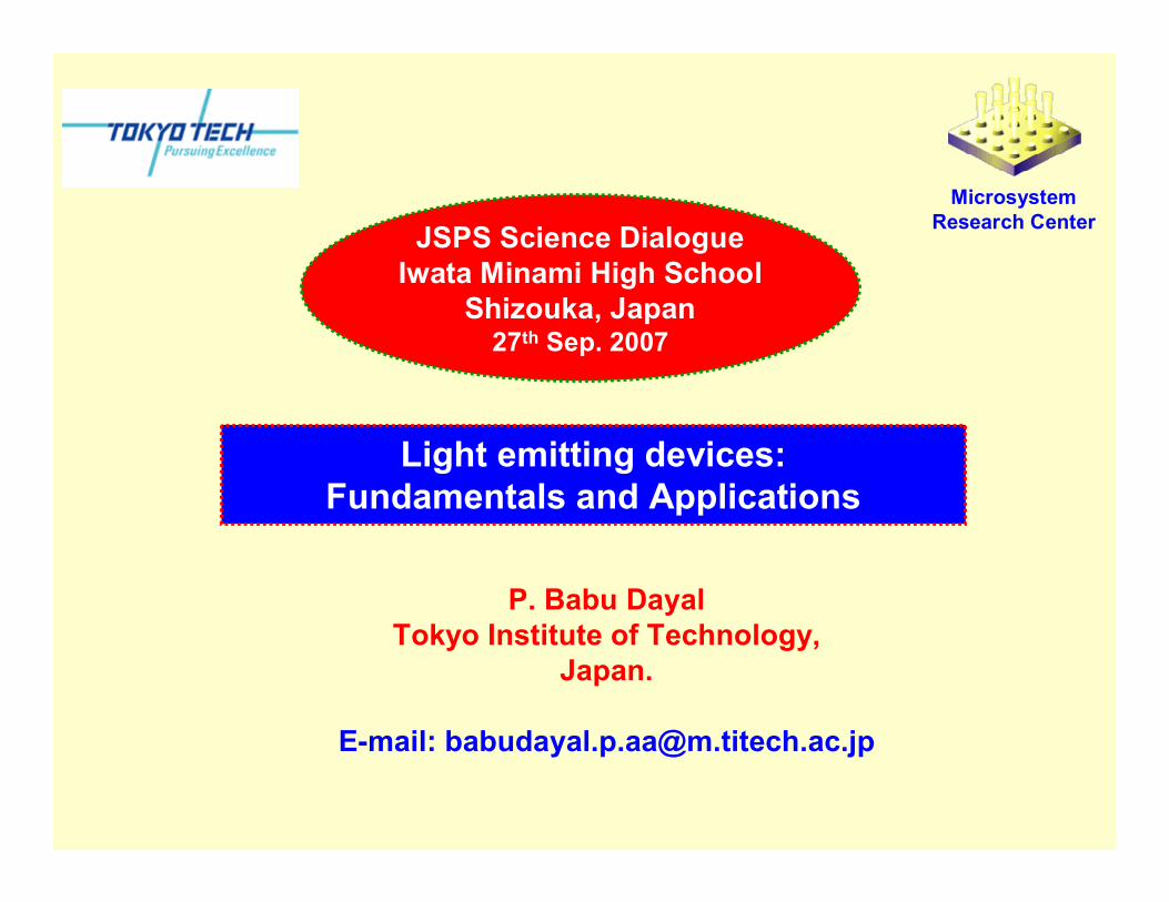
Contents
India in Brief….
Semiconductors
Light Emitting Diode
LASERs
VCSELs
Applications
Fundamentals &
Examples
Part-IA brief introduction to India
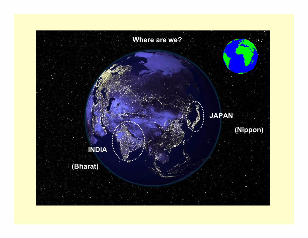
Where are we?
INDIA
JAPAN
(Bharat)
(Nippon)

Humble Greetings
NAMASTE Koninchiwa
India Japan
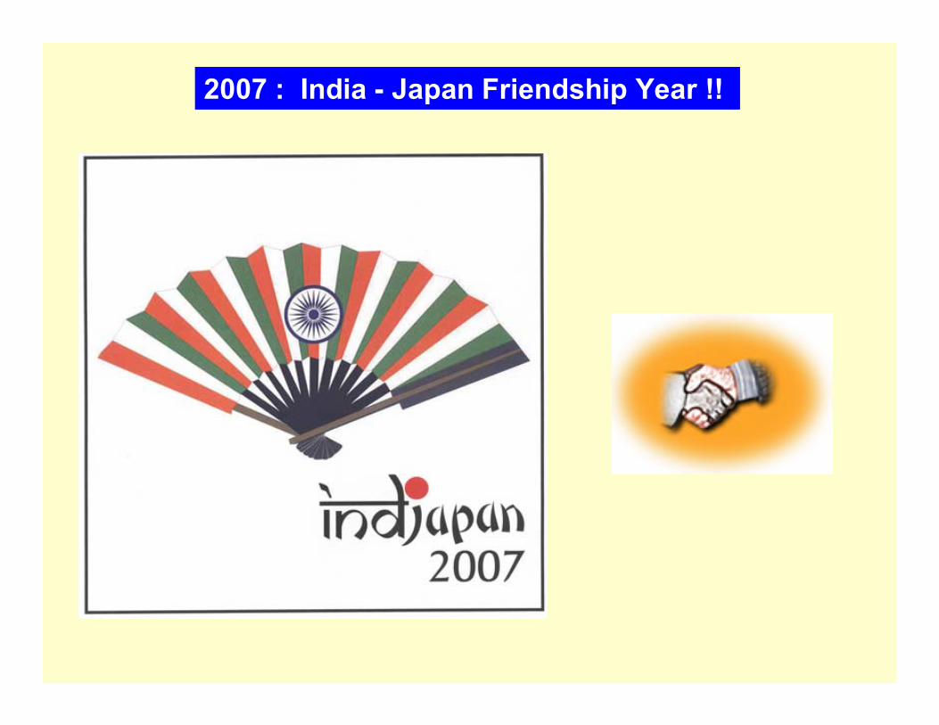
2007 : India - Japan Friendship Year !!
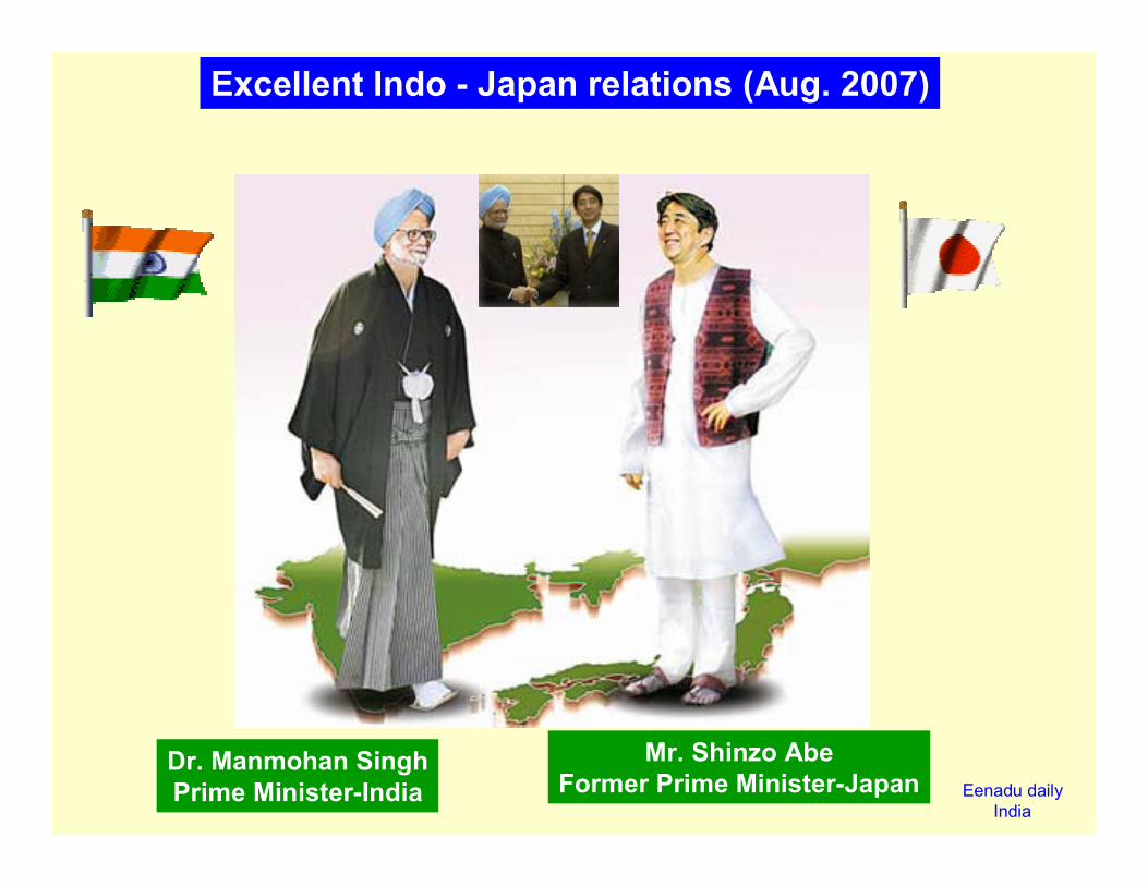
Excellent Indo - Japan relations (Aug. 2007)
Dr. Manmohan SinghPrime Minister-India
Mr. Shinzo AbeFormer Prime Minister-Japan Eenadu daily
India
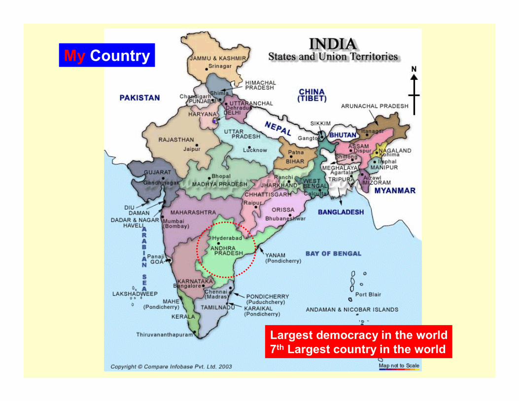
Largest democracy in the world7th Largest country in the world
My Country
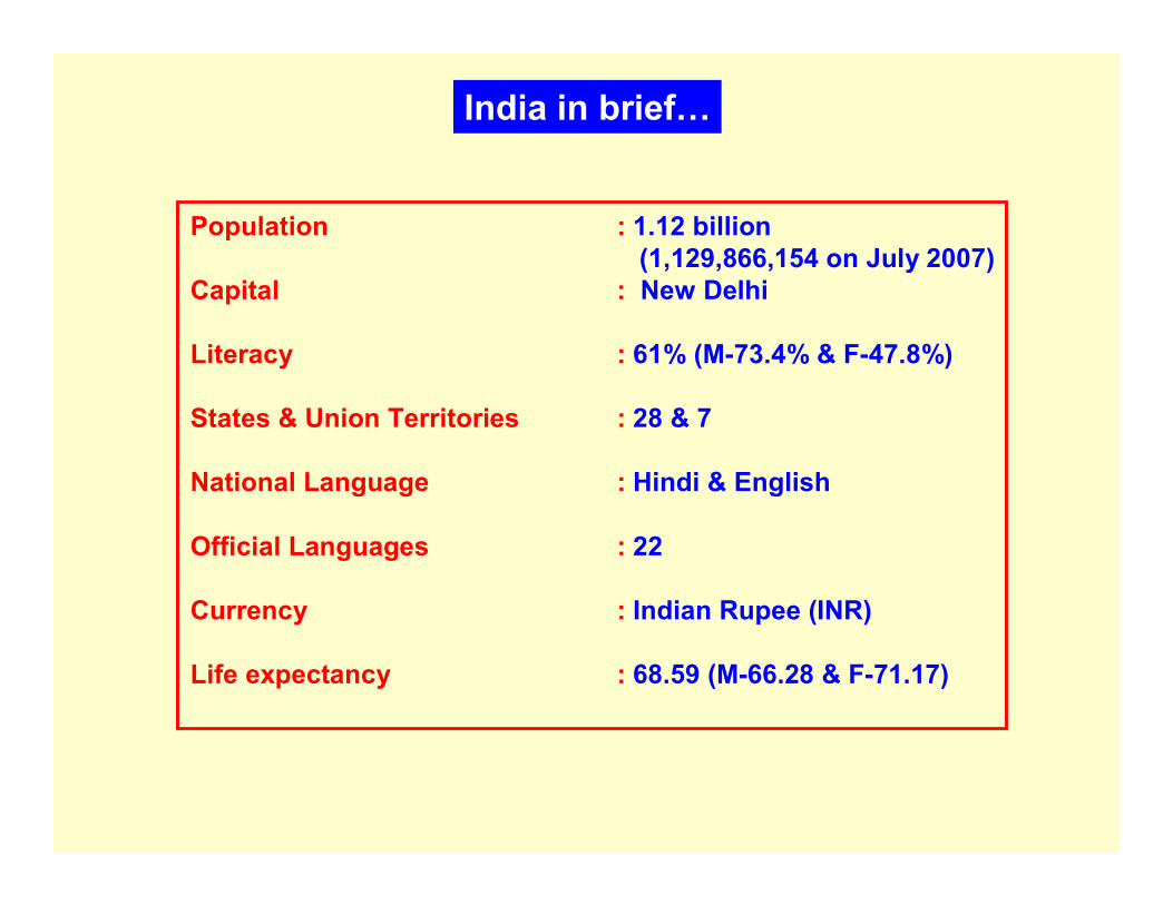
India in brief…
Population : 1.12 billion(1,129,866,154 on July 2007)
Capital : New Delhi
Literacy : 61% (M-73.4% & F-47.8%)
States & Union Territories : 28 & 7
National Language : Hindi & English
Official Languages : 22
Currency : Indian Rupee (INR)
Life expectancy : 68.59 (M-66.28 & F-71.17)
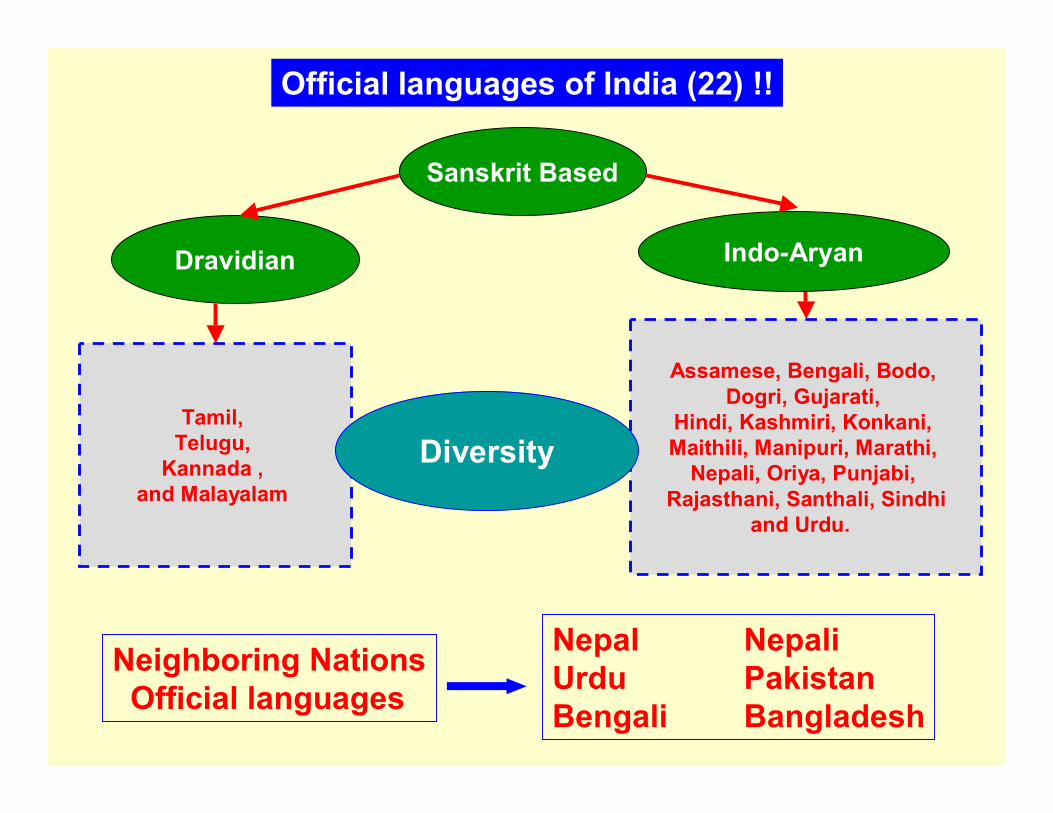
Official languages of India (22) !!
Dravidian Indo-Aryan
Tamil, Telugu,
Kannada , and Malayalam
Assamese, Bengali, Bodo, Dogri, Gujarati,
Hindi, Kashmiri, Konkani, Maithili, Manipuri, Marathi,
Nepali, Oriya, Punjabi, Rajasthani, Santhali, Sindhi
and Urdu.
Sanskrit Based
Nepal NepaliUrdu PakistanBengali Bangladesh
Neighboring NationsOfficial languages
Diversity
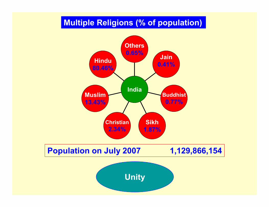
Hindu80.46%
Muslim13.43%
Christian2.34%
Sikh1.87%
Buddhist0.77%
Jain0.41%
Others0.65%
India
Multiple Religions (% of population)
Unity
Population on July 2007 1,129,866,154

My City-Rajahmundry with Godavari River
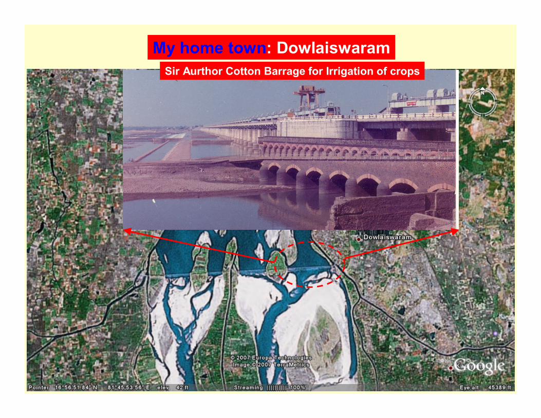
My home town: DowlaiswaramSir Aurthor Cotton Barrage for Irrigation of crops
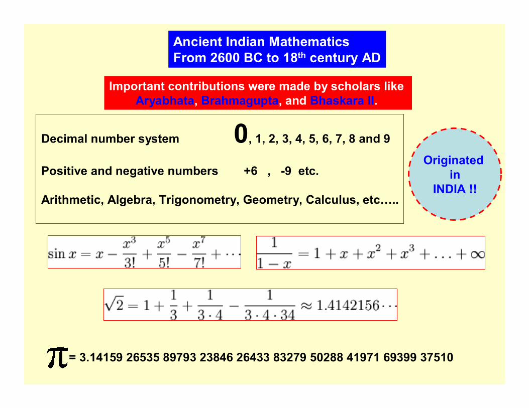
Ancient Indian MathematicsFrom 2600 BC to 18th century AD
Decimal number system 0, 1, 2, 3, 4, 5, 6, 7, 8 and 9
Positive and negative numbers +6 , -9 etc.
Arithmetic, Algebra, Trigonometry, Geometry, Calculus, etc…..
Important contributions were made by scholars like Aryabhata, Brahmagupta, and Bhaskara II.
= 3.14159 26535 89793 23846 26433 83279 50288 41971 69399 37510
Originated in
INDIA !!
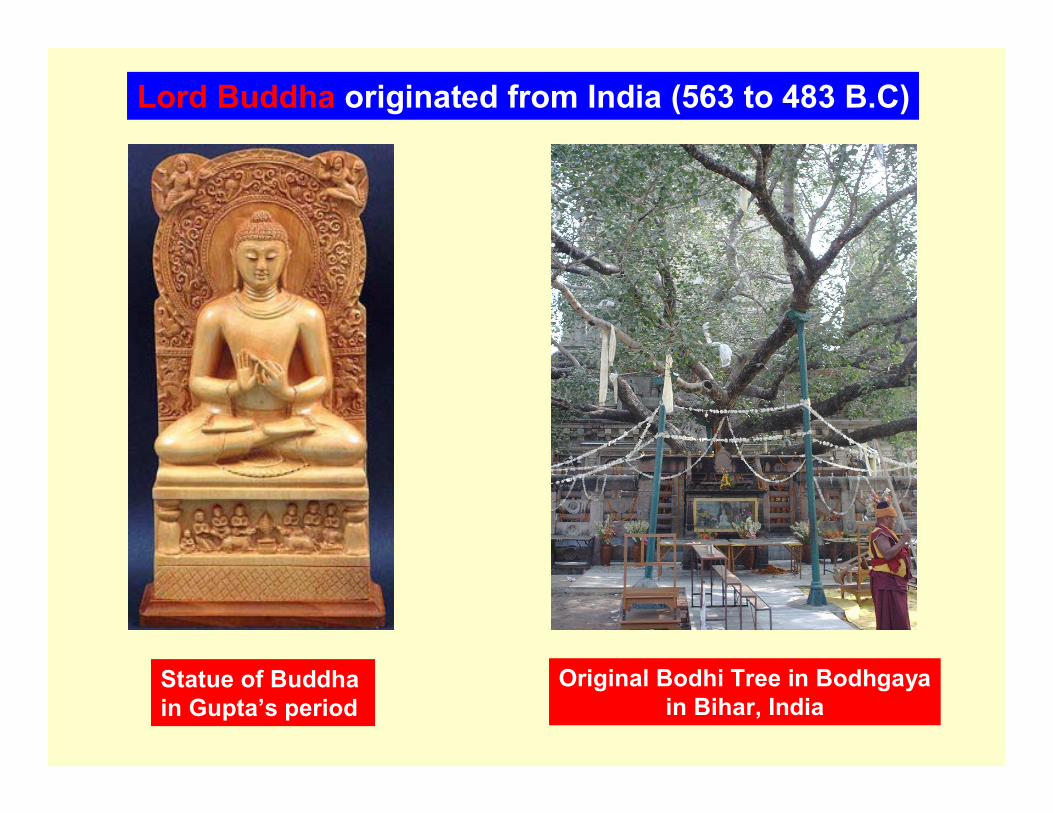
Lord Buddha originated from India (563 to 483 B.C)
Statue of Buddha in Gupta’s period
Original Bodhi Tree in Bodhgayain Bihar, India

Takshila, Nalanda university(First centers of higher learning in the world, 300 BC)
Nalanda was not a formal college or university. Instead there were renownedteachers who taught various subjects like medicine, astronomy, astrology,
Commerce, accountancy, law, magic, music, painting, crafts, archery and the study of the Vedas. Students sought admission when they were about 16.
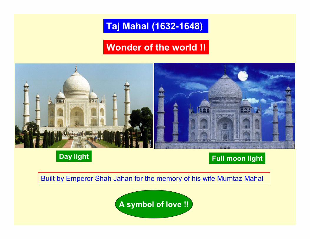
Taj Mahal (1632-1648)
Day light Full moon light
Built by Emperor Shah Jahan for the memory of his wife Mumtaz Mahal
A symbol of love !!
Wonder of the world !!

Popular Arts
Kuchipudi, the traditional dance of
Andhara pradesh
Bharatanatyam-Indian Classical Dance
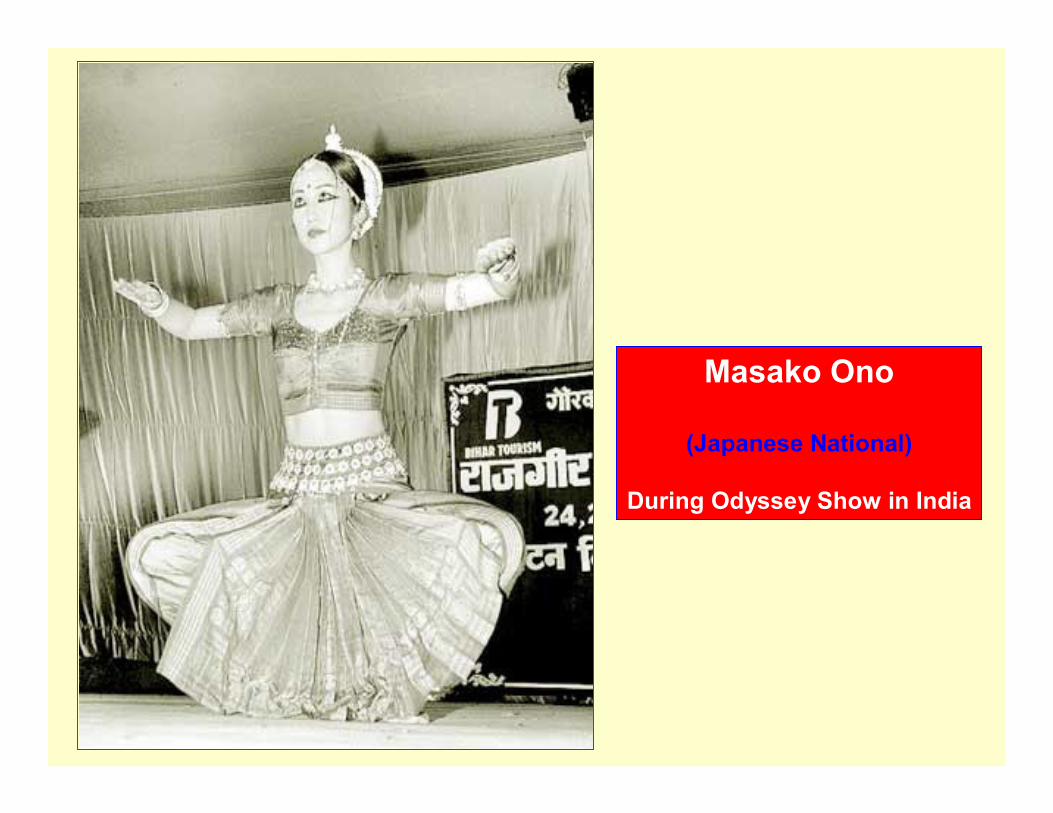
Masako Ono
(Japanese National)
During Odyssey Show in India

Typical food of India
South Indian meals North Indian meals
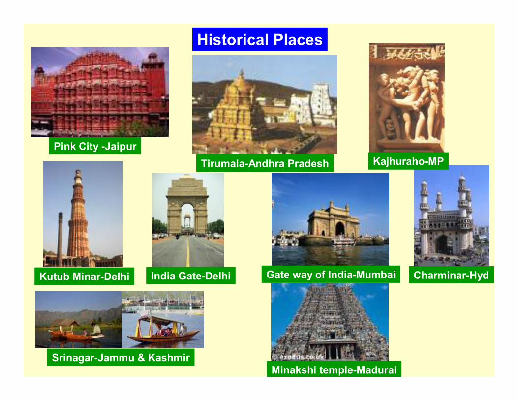
Historical Places
Pink City -JaipurTirumala-Andhra Pradesh Kajhuraho-MP
Kutub Minar-Delhi Gate way of India-Mumbai Charminar-Hyd
Srinagar-Jammu & KashmirMinakshi temple-Madurai
India Gate-Delhi
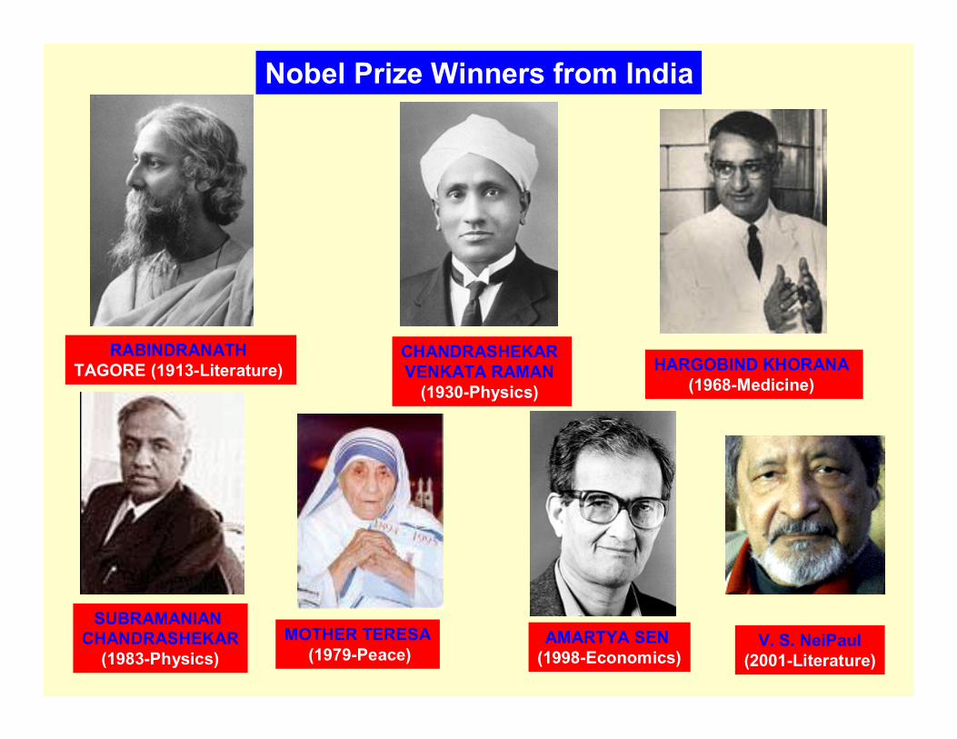
RABINDRANATHTAGORE (1913-Literature)
CHANDRASHEKAR VENKATA RAMAN
(1930-Physics) HARGOBIND KHORANA
(1968-Medicine)
SUBRAMANIAN CHANDRASHEKAR
(1983-Physics) AMARTYA SEN
(1998-Economics)
Nobel Prize Winners from India
MOTHER TERESA(1979-Peace)
V. S. NeiPaul(2001-Literature)
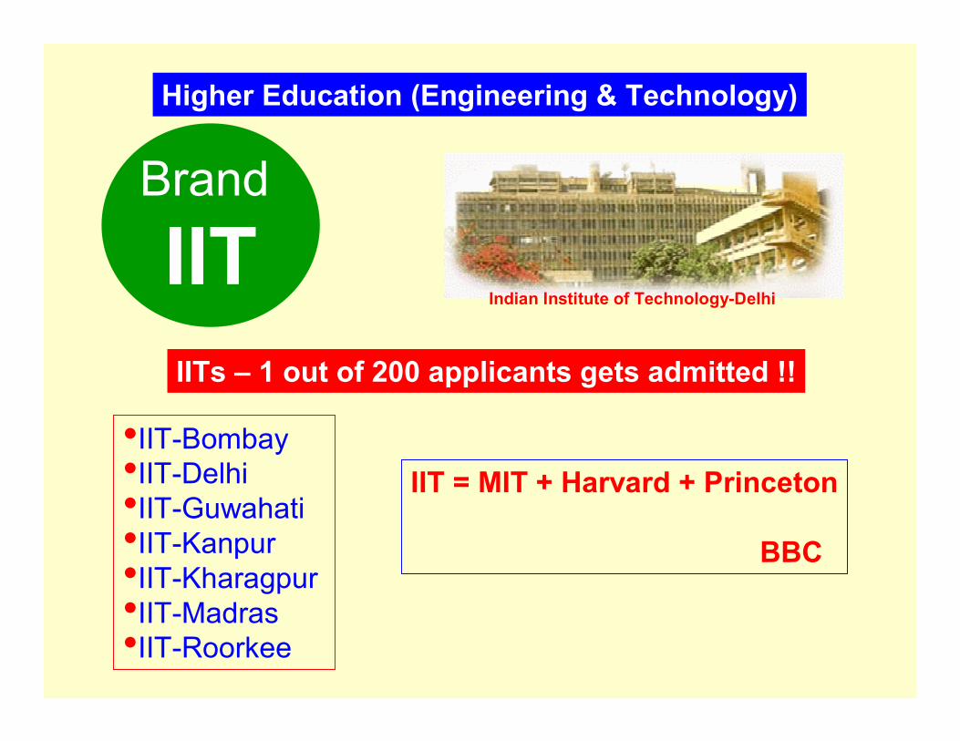
Brand
IIT
Higher Education (Engineering & Technology)
IITs – 1 out of 200 applicants gets admitted !!
Indian Institute of Technology-Delhi
•IIT-Bombay •IIT-Delhi•IIT-Guwahati•IIT-Kanpur•IIT-Kharagpur•IIT-Madras•IIT-Roorkee
IIT = MIT + Harvard + Princeton
BBC
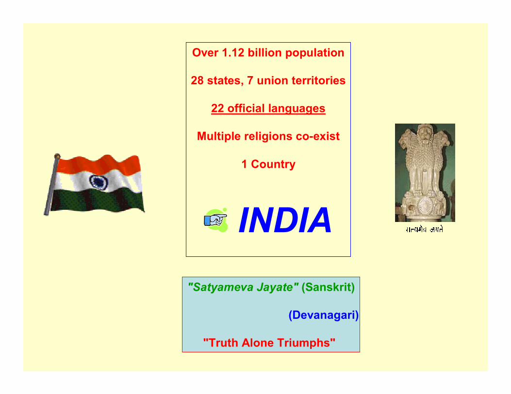
Over 1.12 billion population
28 states, 7 union territories
22 official languages
Multiple religions co-exist
1 Country
INDIA"Satyameva Jayate" (Sanskrit)
������� ���� (Devanagari)
"Truth Alone Triumphs"
Part-IILight Emitting Devices
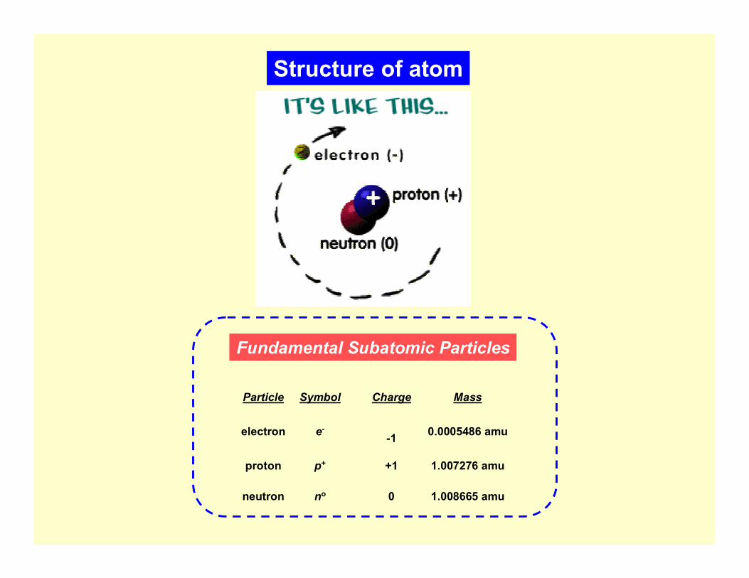
Structure of atom
Fundamental Subatomic Particles
1.008665 amu0 noneutron
1.007276 amu+1 p+proton
0.0005486 amu-1 e-electron
MassChargeSymbol Particle
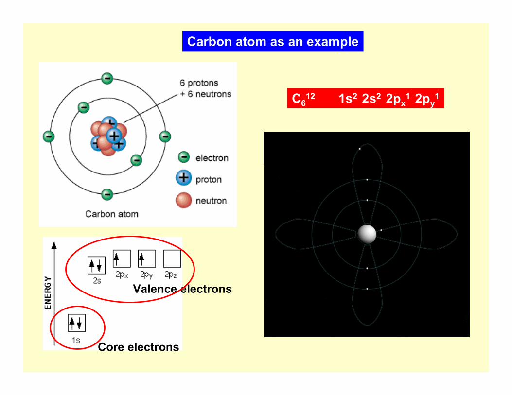
Carbon atom as an example
Core electrons
Valence electrons
C612 1s2 2s2 2px
1 2py1

Bohr’s Postulates Energy Levels
Electrons can change orbits by radiating (larger to smaller), absorbing radiation (smaller to larger) or by collisions (either larger to smaller or smaller to larger).
Lower
Higher
Abs
orpt
ion
Emis
sion
Dr. Niels Bohr, Denmark (1913)
http://en.wikipedia.org/wiki/Niels_Bohr
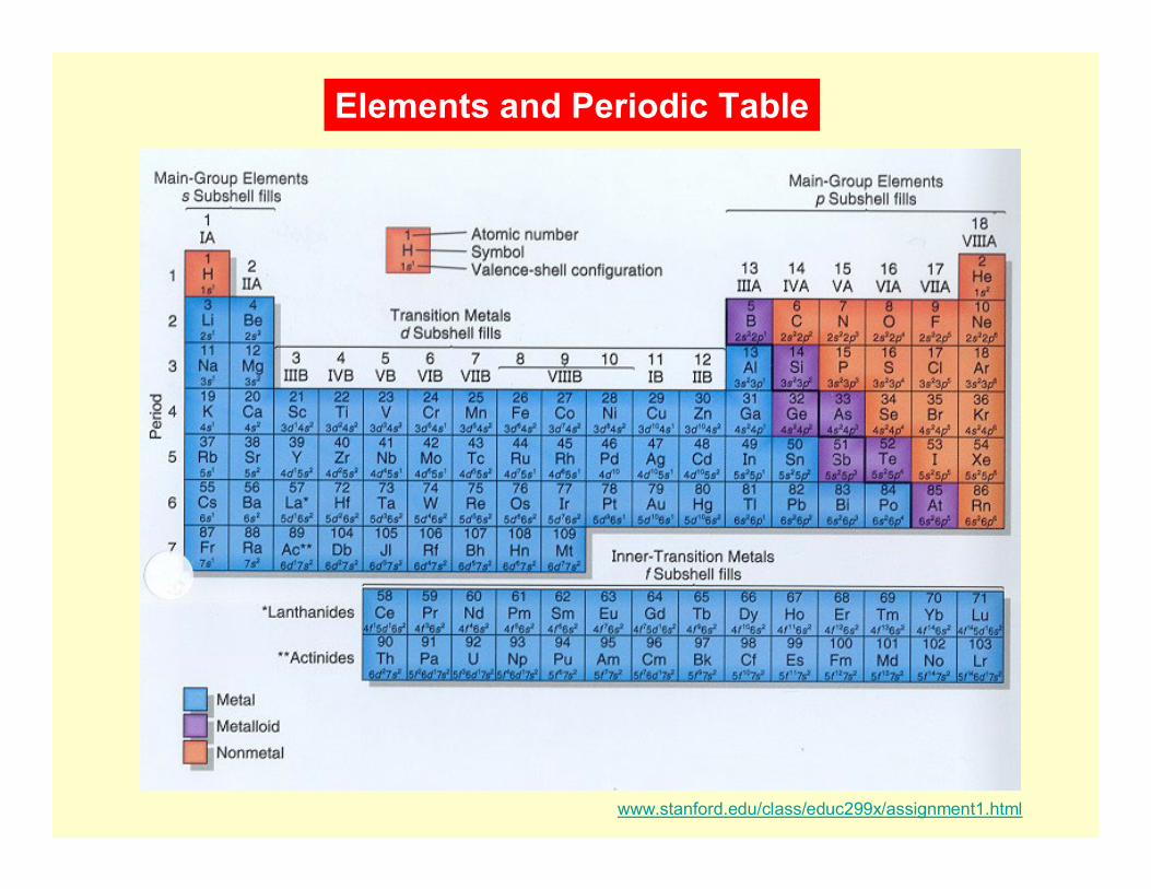
Elements and Periodic Table
www.stanford.edu/class/educ299x/assignment1.html
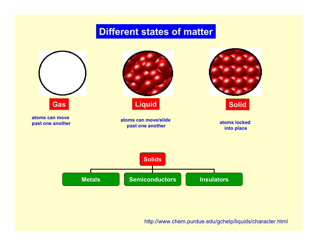
Different states of matter
Gas Liquid Solid
http://www.chem.purdue.edu/gchelp/liquids/character.html
atoms can move past one another
atoms can move/slide past one another
atoms locked into place
Solids
Metals Semiconductors Insulators
http://www.physics.udel.edu/~watson/ALLSTEL99/sld007.htm
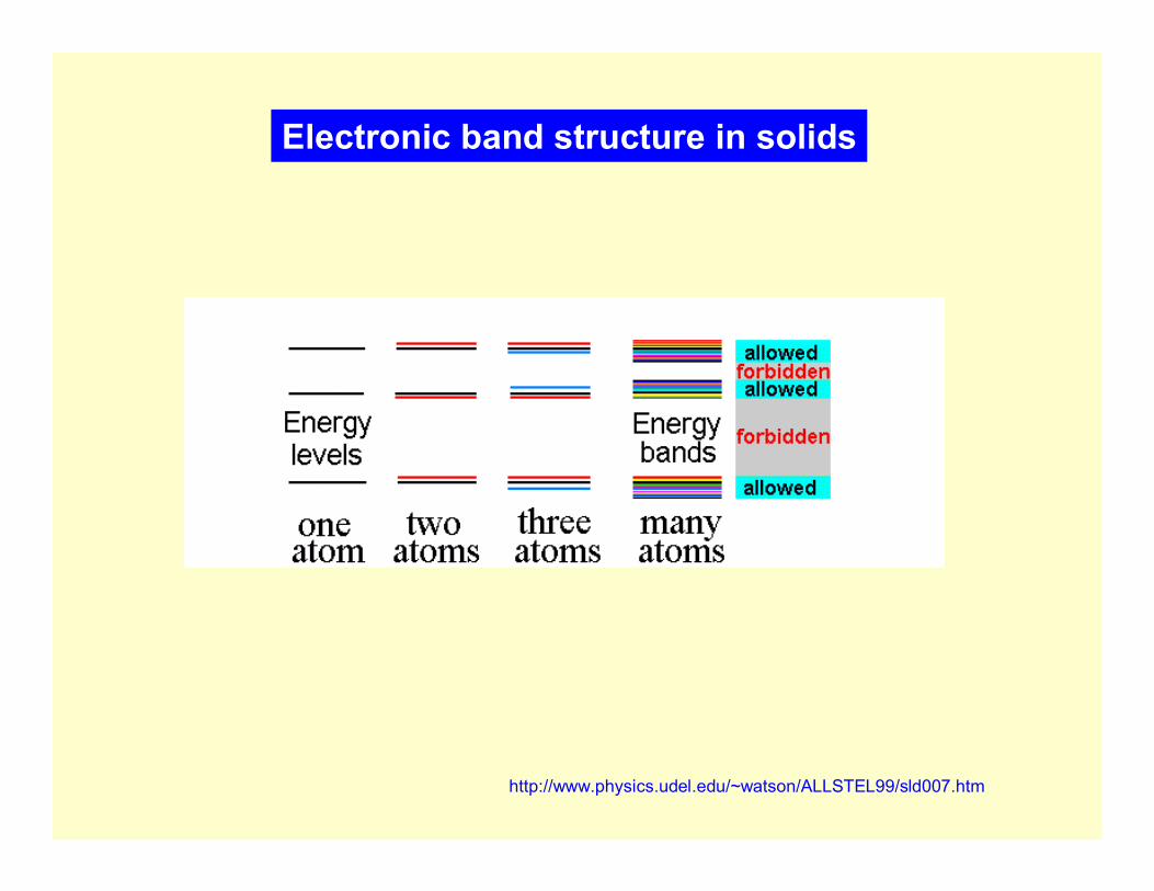
Electronic band structure in solids
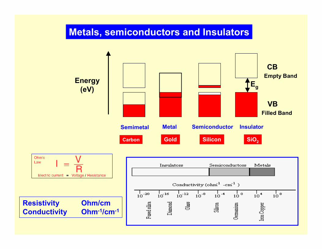
Metals, semiconductors and Insulators
CB
VB
Eg
Semimetal Metal Semiconductor Insulator
Energy(eV)
Carbon Gold Silicon SiO2
Filled Band
Empty Band
Resistivity Ohm/cmConductivity Ohm-1/cm-1
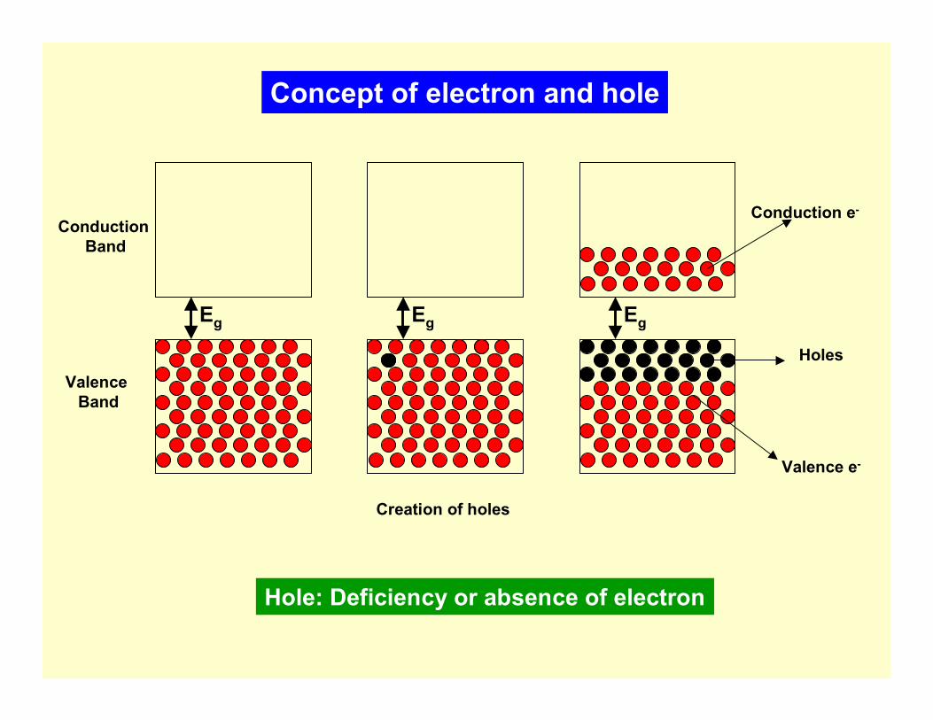
Concept of electron and hole
EgEg
Hole: Deficiency or absence of electron
ConductionBand
ValenceBand
Creation of holes
Eg
Conduction e-
Holes
Valence e-
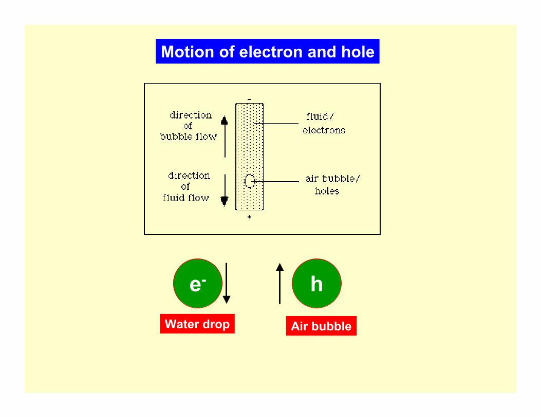
e- hWater drop Air bubble
Motion of electron and hole
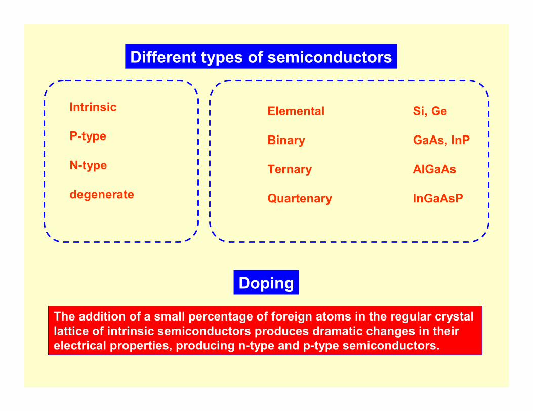
Different types of semiconductors
Elemental Si, Ge
Binary GaAs, InP
Ternary AlGaAs
Quartenary InGaAsP
Intrinsic
P-type
N-type
degenerate
Doping
The addition of a small percentage of foreign atoms in the regular crystallattice of intrinsic semiconductors produces dramatic changes in their electrical properties, producing n-type and p-type semiconductors.
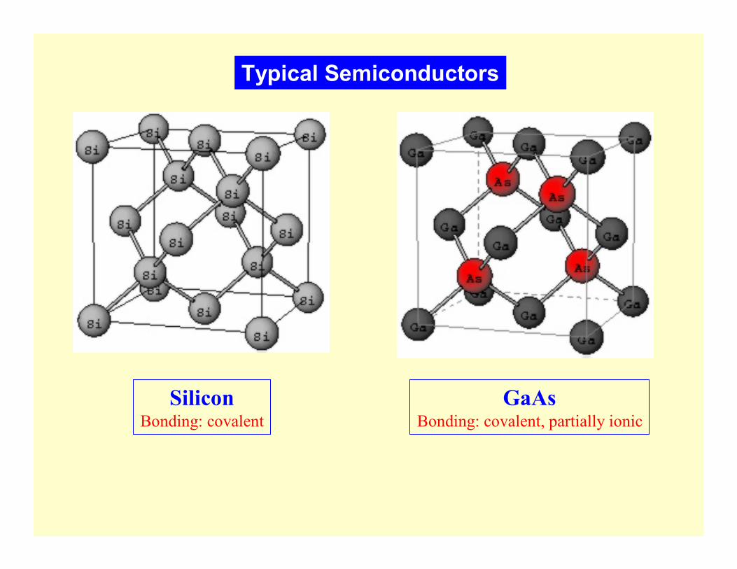
GaAsBonding: covalent, partially ionic
SiliconBonding: covalent
Typical Semiconductors
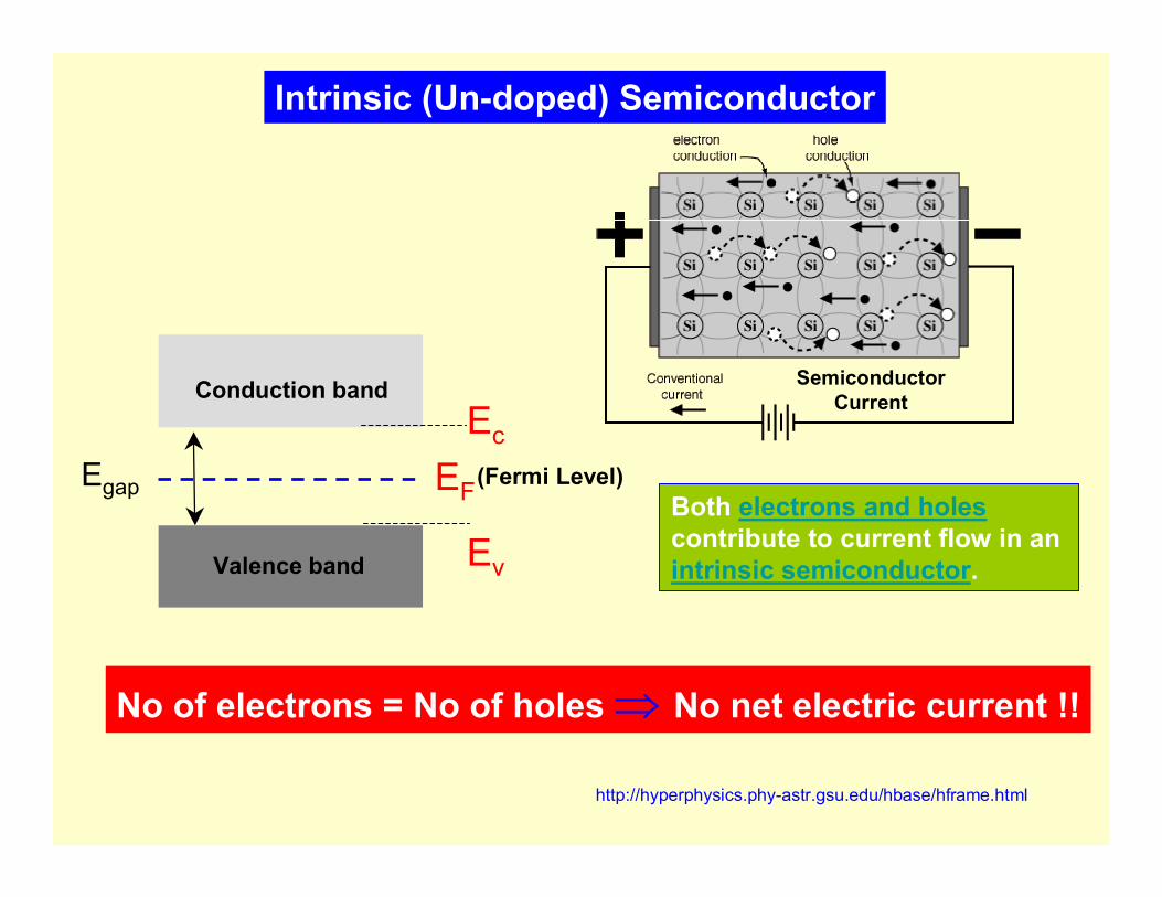
Intrinsic (Un-doped) Semiconductor
Semiconductor Current
Both electrons and holescontribute to current flow in an intrinsic semiconductor.
http://hyperphysics.phy-astr.gsu.edu/hbase/hframe.html
EF
Conduction band
Valence band
Egap (Fermi Level)
No of electrons = No of holes ⇒ No net electric current !!
Ec
Ev
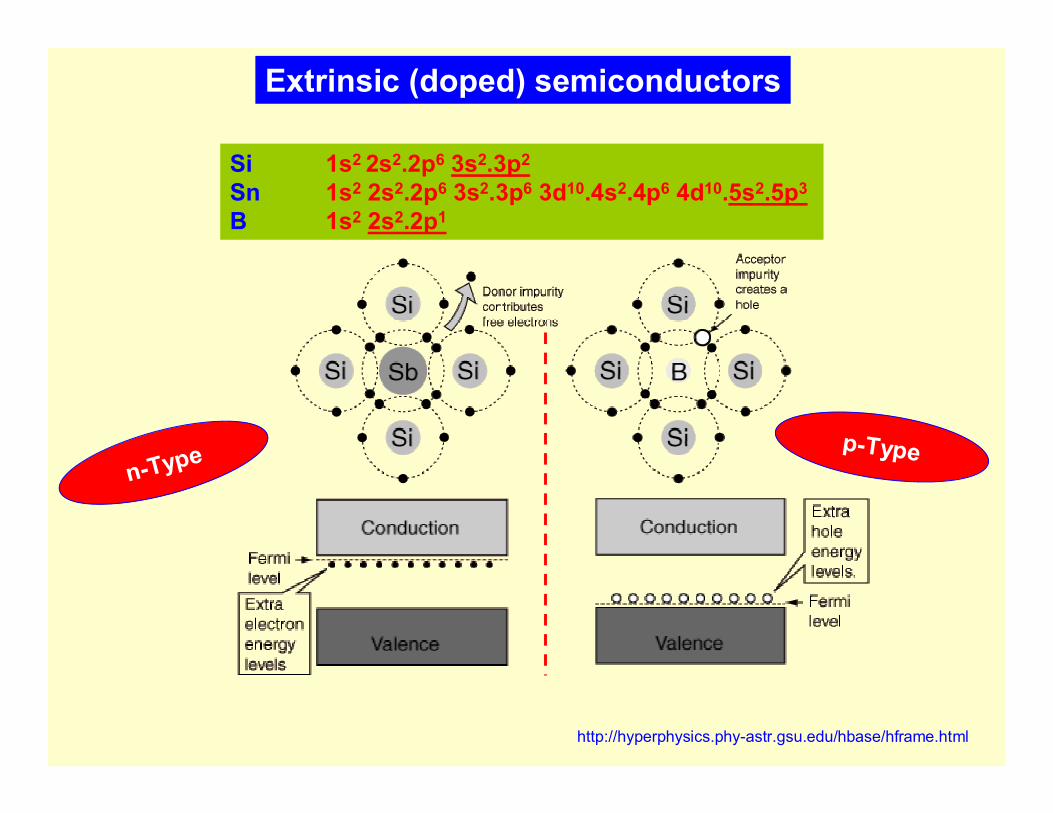
Extrinsic (doped) semiconductors
Si 1s2 2s2.2p6 3s2.3p2
Sn 1s2 2s2.2p6 3s2.3p6 3d10.4s2.4p6 4d10.5s2.5p3
B 1s2 2s2.2p1
n-Type p-Type
http://hyperphysics.phy-astr.gsu.edu/hbase/hframe.html
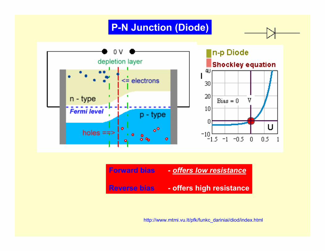
P-N Junction (Diode)
http://www.mtmi.vu.lt/pfk/funkc_dariniai/diod/index.html
Forward bias - offers low resistance
Reverse bias - offers high resistance
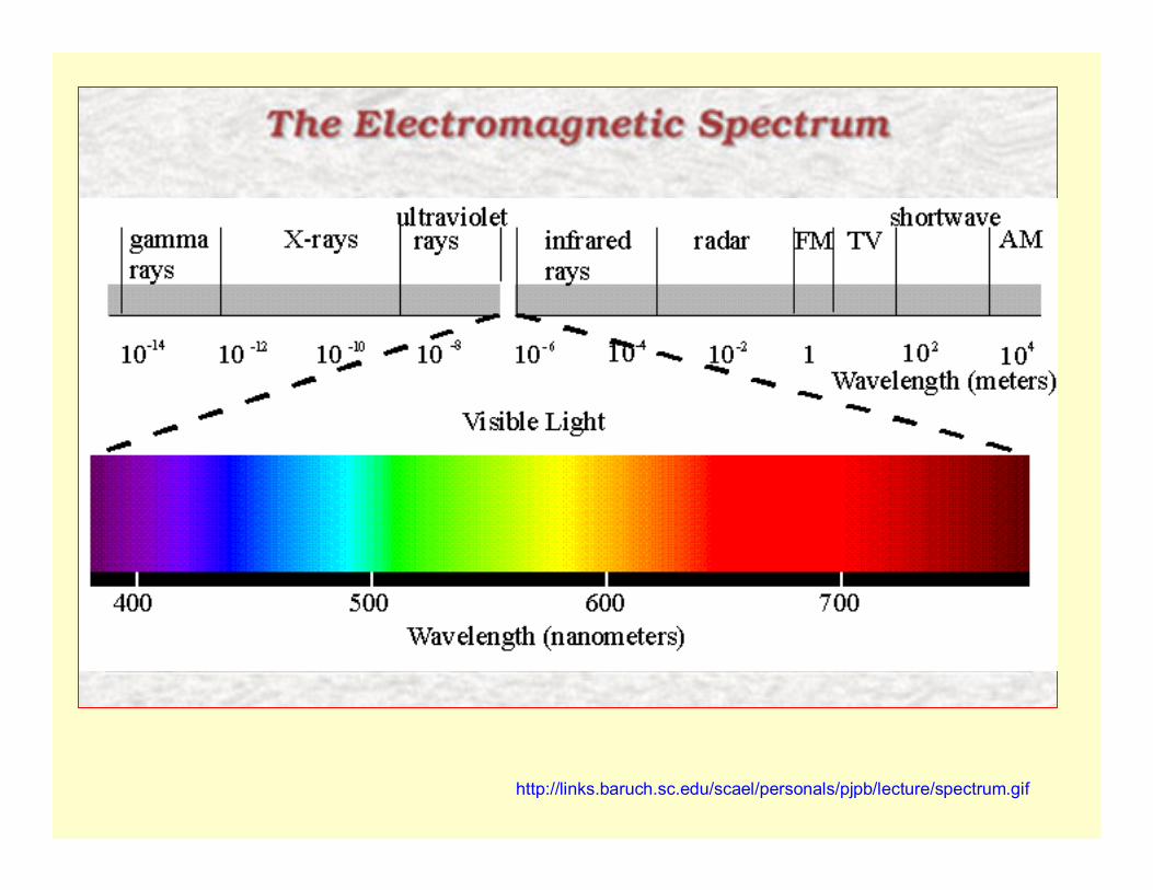
http://links.baruch.sc.edu/scael/personals/pjpb/lecture/spectrum.gif
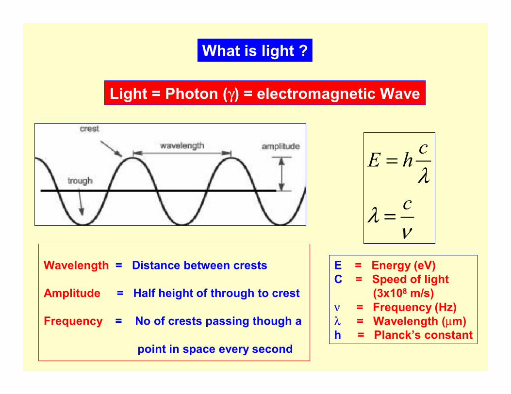
Light = Photon (γ) = electromagnetic Wave
Wavelength = Distance between crests
Amplitude = Half height of through to crest
Frequency = No of crests passing though a
point in space every second
cE h
cλ
λν
=
=
E = Energy (eV)C = Speed of light
(3x10⁸ m/s)ν = Frequency (Hz)λ = Wavelength (µm)h = Planck’s constant
What is light ?
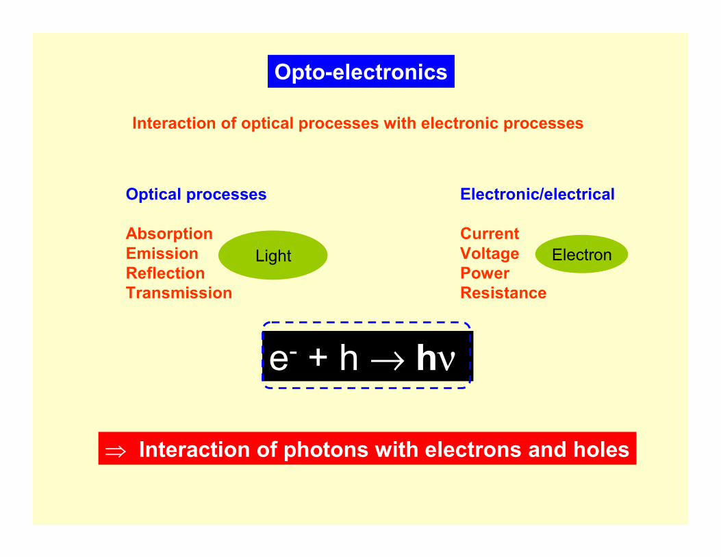
Interaction of optical processes with electronic processes
Optical processes
AbsorptionEmissionReflectionTransmission
Electronic/electrical
CurrentVoltagePowerResistance
Light Electron
Opto-electronics
⇒ Interaction of photons with electrons and holes
e- + h → hν
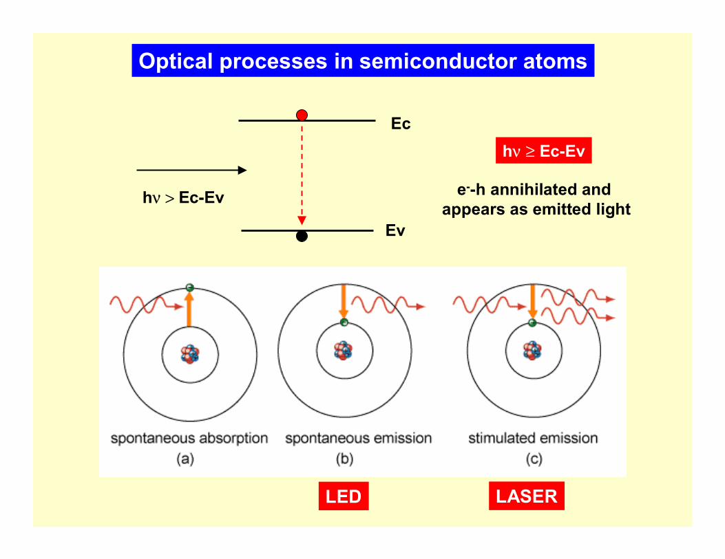
LED
Optical processes in semiconductor atoms
LASER
hν > Ec-Ev
Ev
Echν ≥ Ec-Ev
e--h annihilated and appears as emitted light
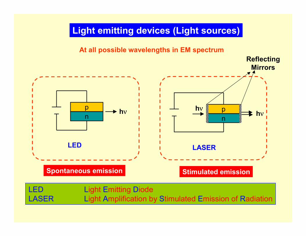
Light emitting devices (Light sources)
At all possible wavelengths in EM spectrum
pn
hν pn
hνhν
LED LASER
ReflectingMirrors
LED Light Emitting DiodeLASER Light Amplification by Stimulated Emission of Radiation
Spontaneous emission Stimulated emission
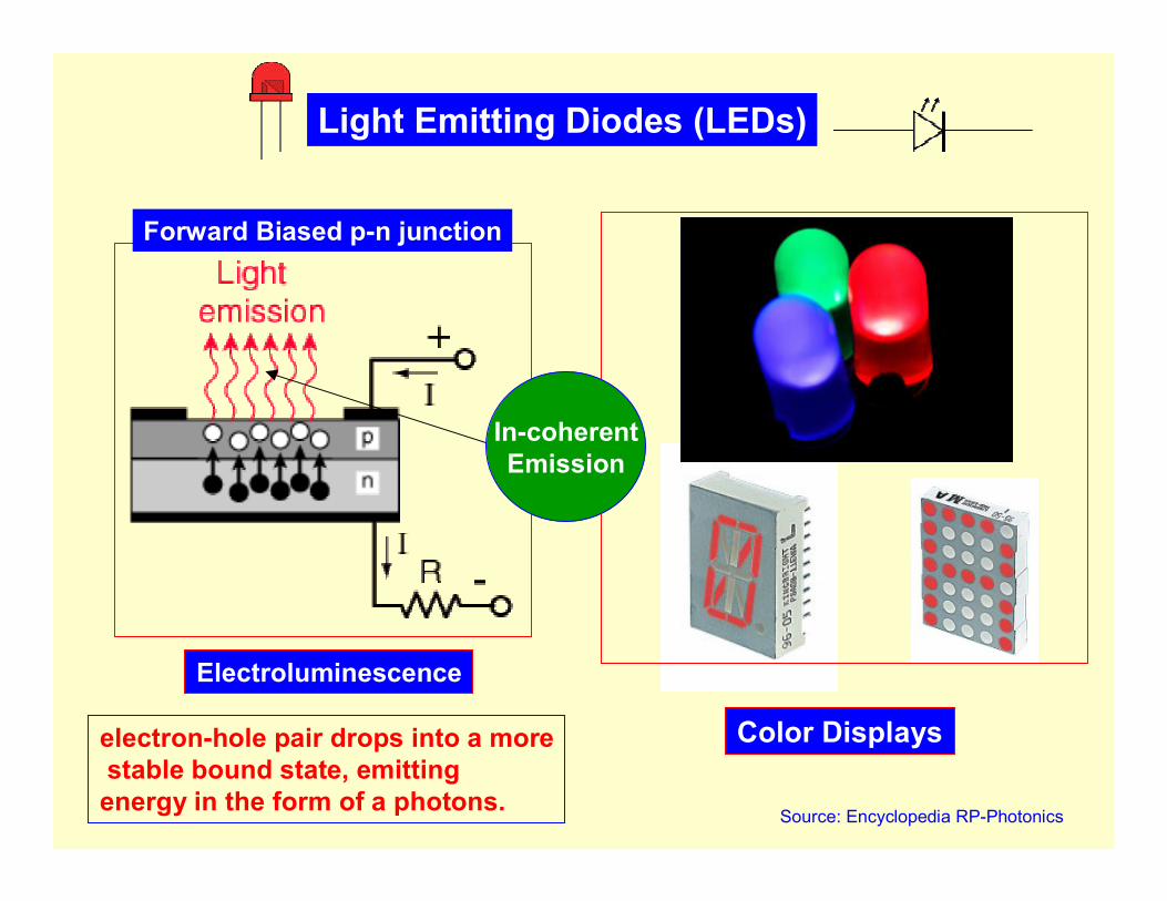
Light Emitting Diodes (LEDs)
Color Displays
Forward Biased p-n junction
Electroluminescence
electron-hole pair drops into a morestable bound state, emitting
energy in the form of a photons. Source: Encyclopedia RP-Photonics
In-coherentEmission
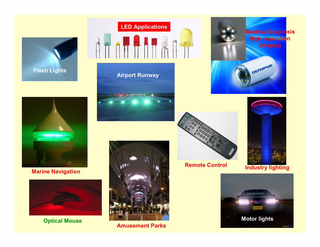
Optical Mouse
Marine Navigation
Amusement Parks
Airport Runway
Medical DiagnosisHigh resolution
Imaging
Motor lights
Industry lighting
Flash Lights
Remote Control
LED Applications
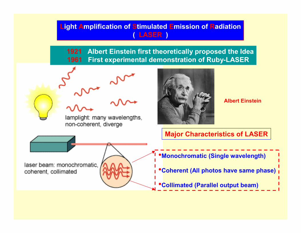
1921 Albert Einstein first theoretically proposed the Idea1961 First experimental demonstration of Ruby-LASER
Light Amplification of Stimulated Emission of Radiation( LASER )
Major Characteristics of LASER
•Monochromatic (Single wavelength)
•Coherent (All photos have same phase)
•Collimated (Parallel output beam)
Albert Einstein
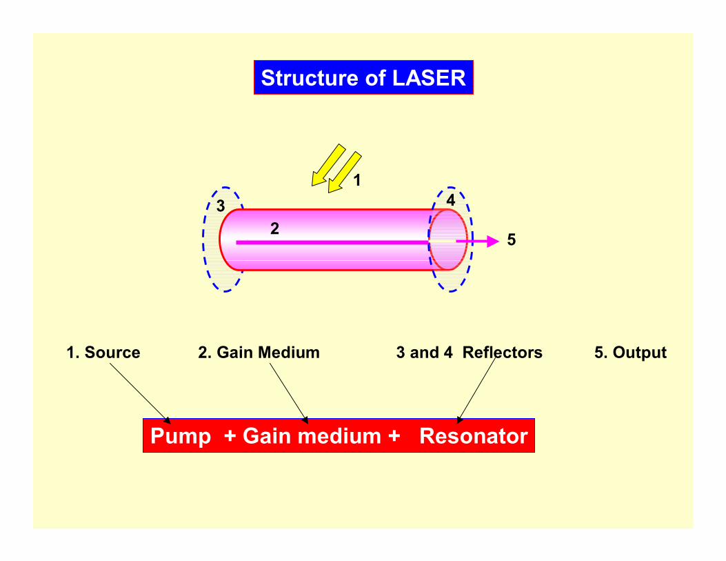
Structure of LASER
23 4
1
5
1. Source 2. Gain Medium 3 and 4 Reflectors 5. Output
Pump + Gain medium + Resonator
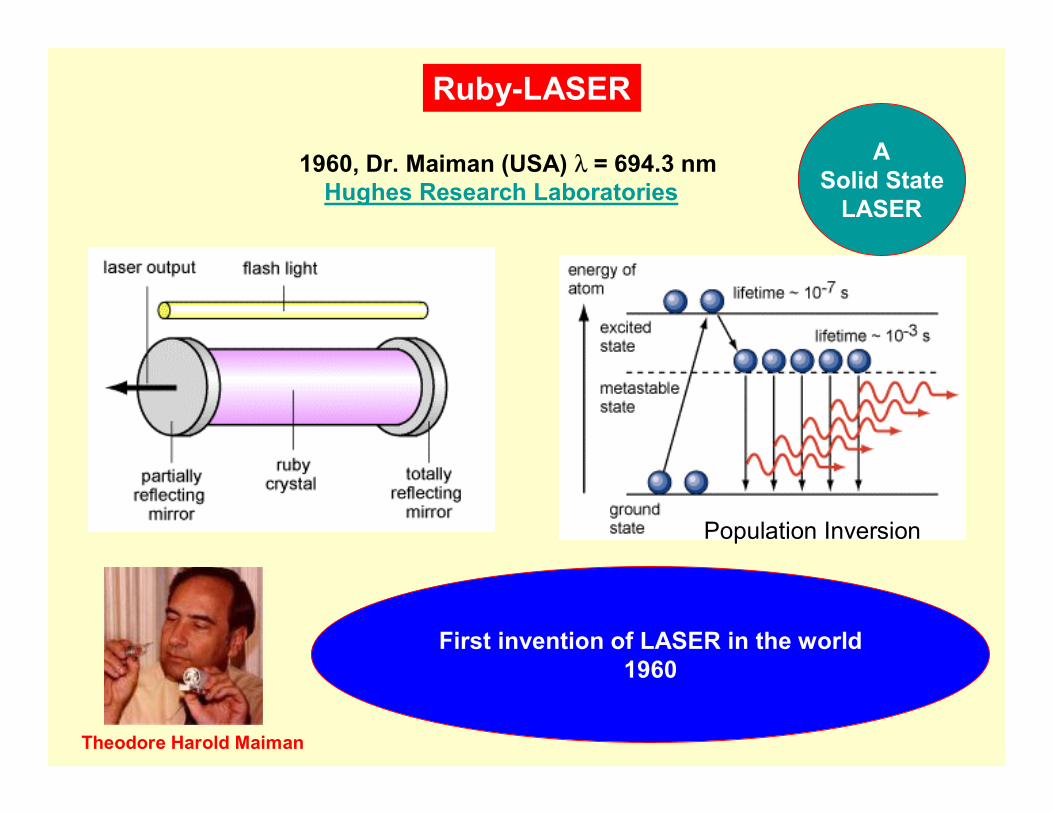
Ruby-LASER
Population Inversion
1960, Dr. Maiman (USA) λ = 694.3 nmHughes Research Laboratories
ASolid State
LASER
First invention of LASER in the world1960
Theodore Harold Maiman
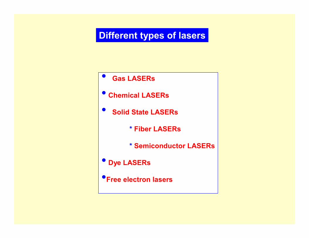
Different types of lasers
• Gas LASERs
• Chemical LASERs
• Solid State LASERs
* Fiber LASERs
* Semiconductor LASERs
• Dye LASERs
•Free electron lasers
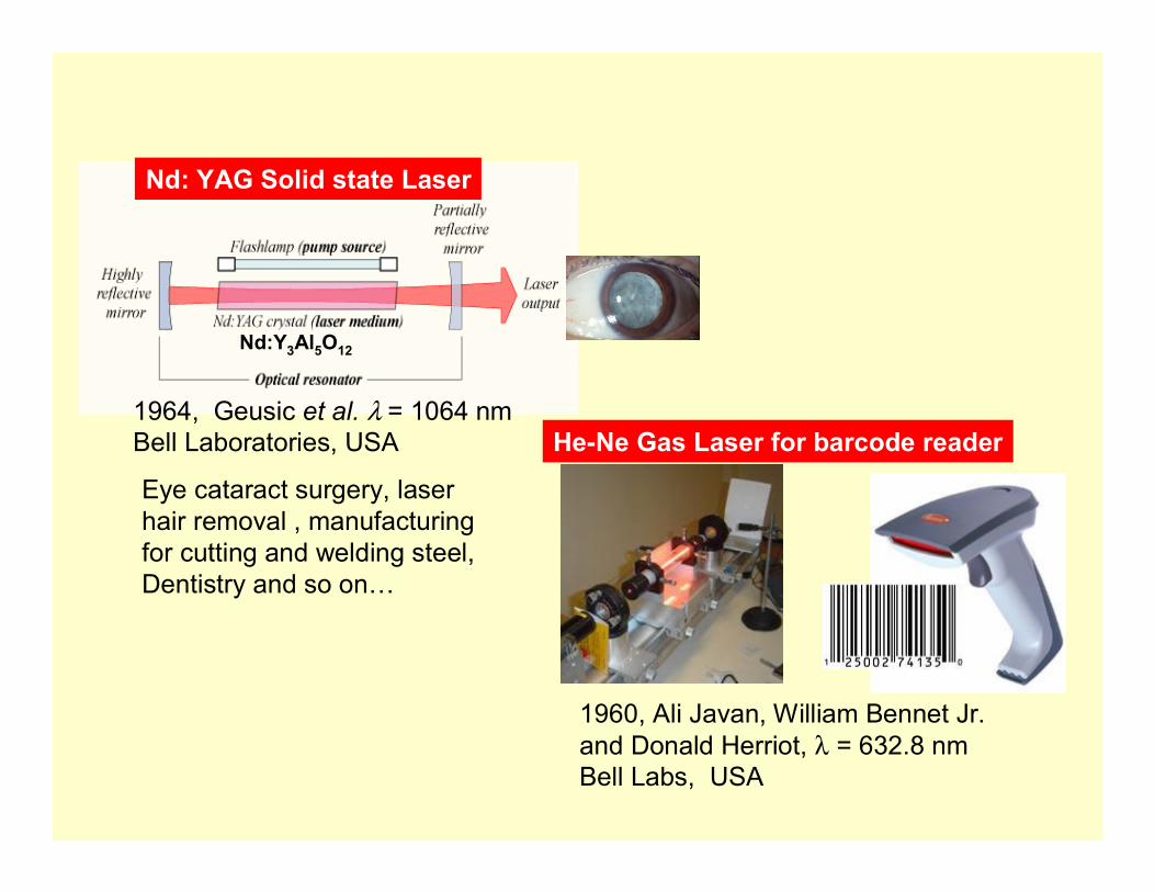
He-Ne Gas Laser for barcode reader
1960, Ali Javan, William Bennet Jr.and Donald Herriot, λ = 632.8 nmBell Labs, USA
Nd:Y3Al5O12
1964, Geusic et al. λ = 1064 nmBell Laboratories, USA
Eye cataract surgery, laser hair removal , manufacturing for cutting and welding steel,Dentistry and so on…
Nd: YAG Solid state Laser

Fiber LASER
The Gain medium of the fiber is doped with rare-earth ions Er3+, Nd3+, Yb3+, Tm3+, Pr3+
Corning Inc. : Low loss optical fiber (1970)
Dye (Liquid) Laser
A table-top dye laser based on Rhodamine 6G, emitting at 580 nm (yellow-orange). Orange dye solution pumped by a 514 nm argon laser (blue-green).
The wide bandwidth makes them particularly suitable for tunable lasers and pulsed lasers.
http://www.alspi.com/laser.htm
Cutting Welding
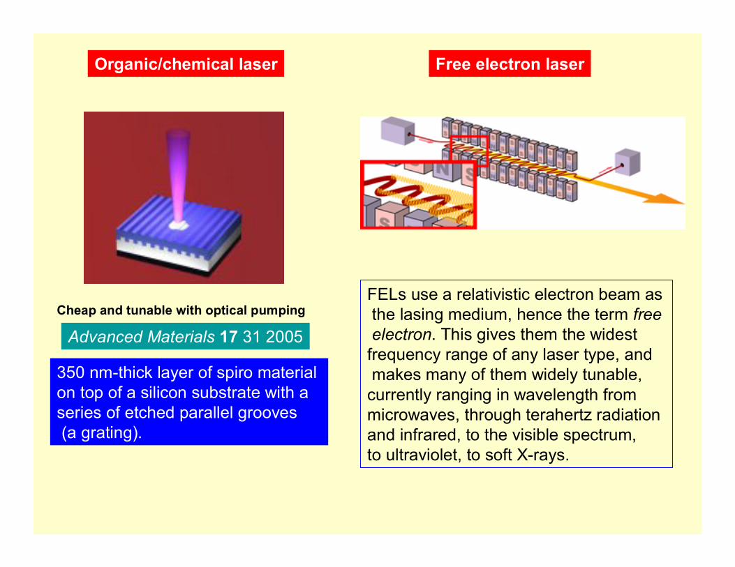
Organic/chemical laser
350 nm-thick layer of spiro material on top of a silicon substrate with a series of etched parallel grooves(a grating).
Cheap and tunable with optical pumping
Advanced Materials 17 31 2005
Free electron laser
FELs use a relativistic electron beam asthe lasing medium, hence the term freeelectron. This gives them the widest
frequency range of any laser type, andmakes many of them widely tunable,
currently ranging in wavelength from microwaves, through terahertz radiationand infrared, to the visible spectrum, to ultraviolet, to soft X-rays.

Semiconductor laser (or) Laser Diode
The most commonly used laser today !!
In their simplest form it consistsof a small rectangular slab of
semiconductor material with two cleaved facets to act as mirrors.
1962 4 different groups
simultaneouslyreported !!
A forward biased p-n junction powered by injected electrical current.
Injection laser diodes
Edge emitting lasers

• Double heterostructure lasers
• Separate confinement lasers
• Distributed feedback lasers
1962-1977-after
Edge emittingOR
In-plane lasers
• Quantum well lasers
• Quantum dot lasers
• Quantum wire lasers
Innovative Research and Development over 3 decades
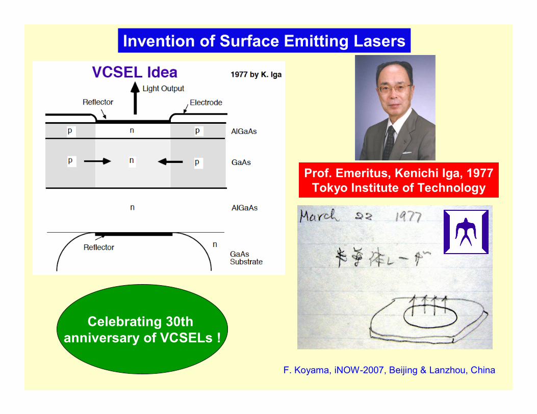
Invention of Surface Emitting Lasers
Prof. Emeritus, Kenichi Iga, 1977Tokyo Institute of Technology
F. Koyama, iNOW-2007, Beijing & Lanzhou, China
Celebrating 30th anniversary of VCSELs !
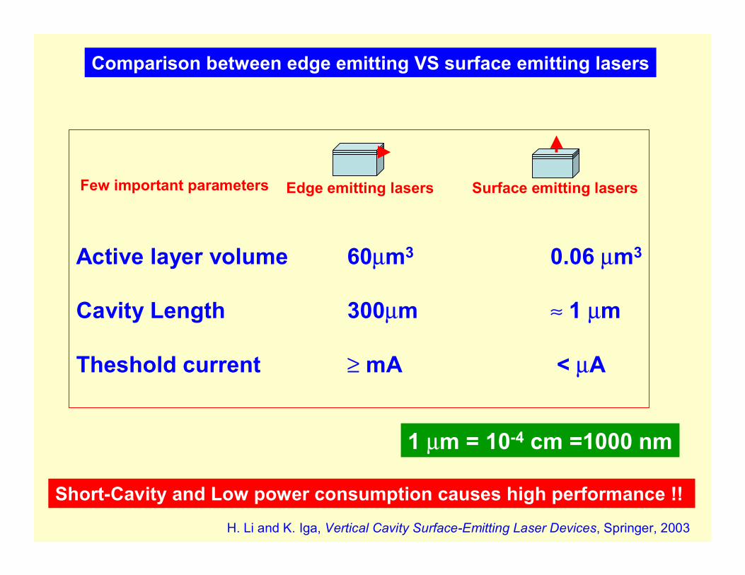
Comparison between edge emitting VS surface emitting lasers
Active layer volume 60µm3 0.06 µm3
Cavity Length 300µm ≈ 1 µm
Theshold current ≥ mA < µA
Edge emitting lasers Surface emitting lasersFew important parameters
Short-Cavity and Low power consumption causes high performance !!
1 µm = 10-4 cm =1000 nm
H. Li and K. Iga, Vertical Cavity Surface-Emitting Laser Devices, Springer, 2003
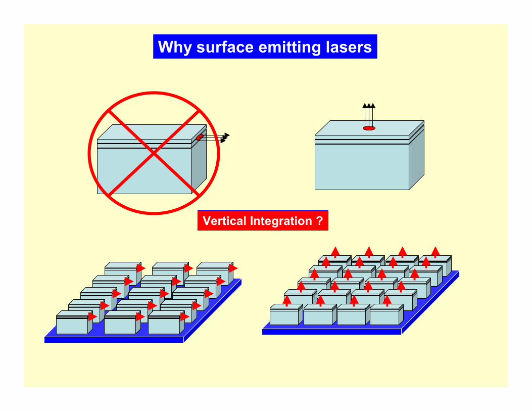
Vertical Integration ?
Why surface emitting lasers
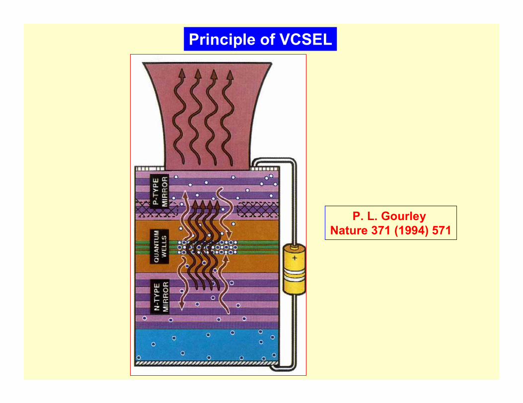
Principle of VCSEL
P. L. GourleyNature 371 (1994) 571
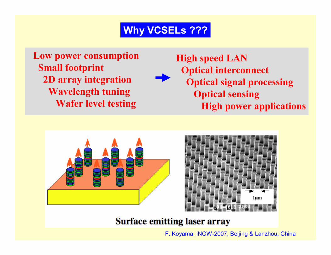
Why VCSELs ???
Low power consumptionSmall footprint 2D array integrationWavelength tuning
Wafer level testing
High speed LANOptical interconnectOptical signal processing
Optical sensingHigh power applications
F. Koyama, iNOW-2007, Beijing & Lanzhou, China
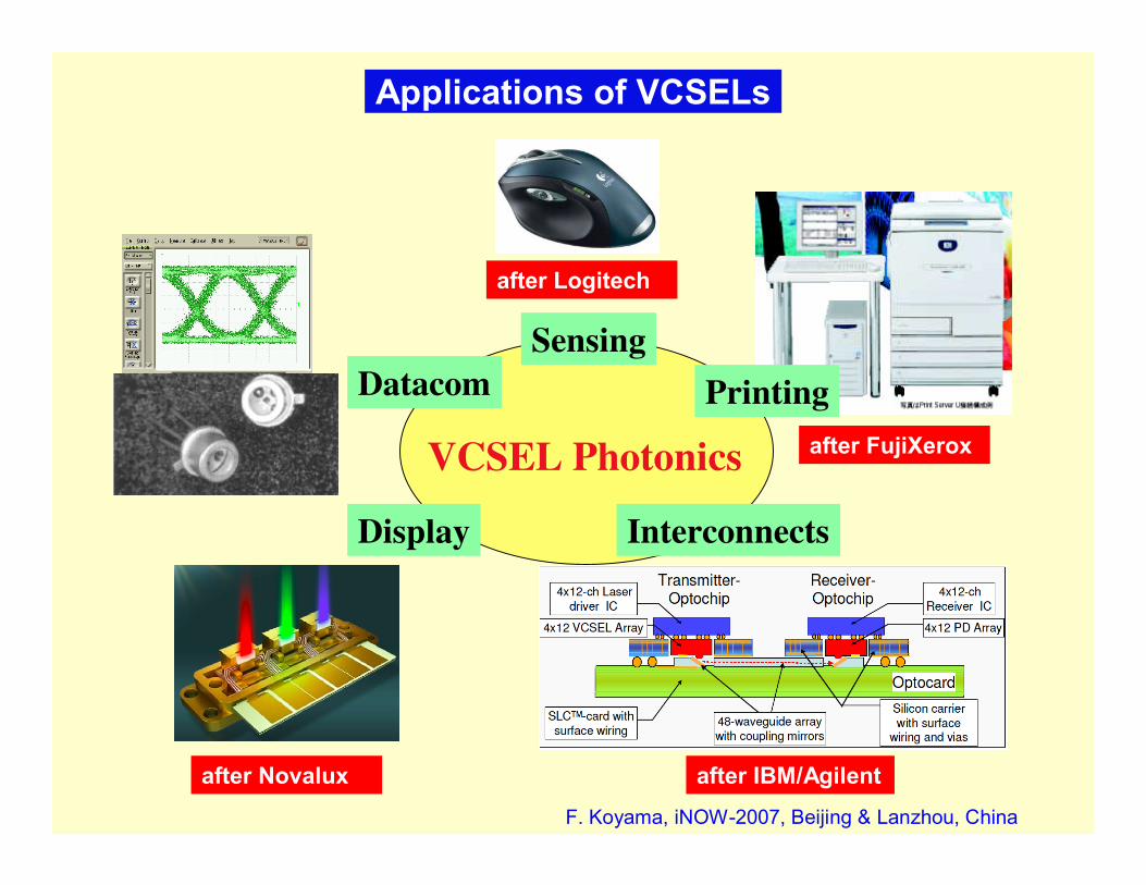
Applications of VCSELs
VCSEL Photonics
Datacom
Display
Sensing
Printing
after Novalux
after FujiXerox
after Logitech
Interconnects
after IBM/AgilentF. Koyama, iNOW-2007, Beijing & Lanzhou, China
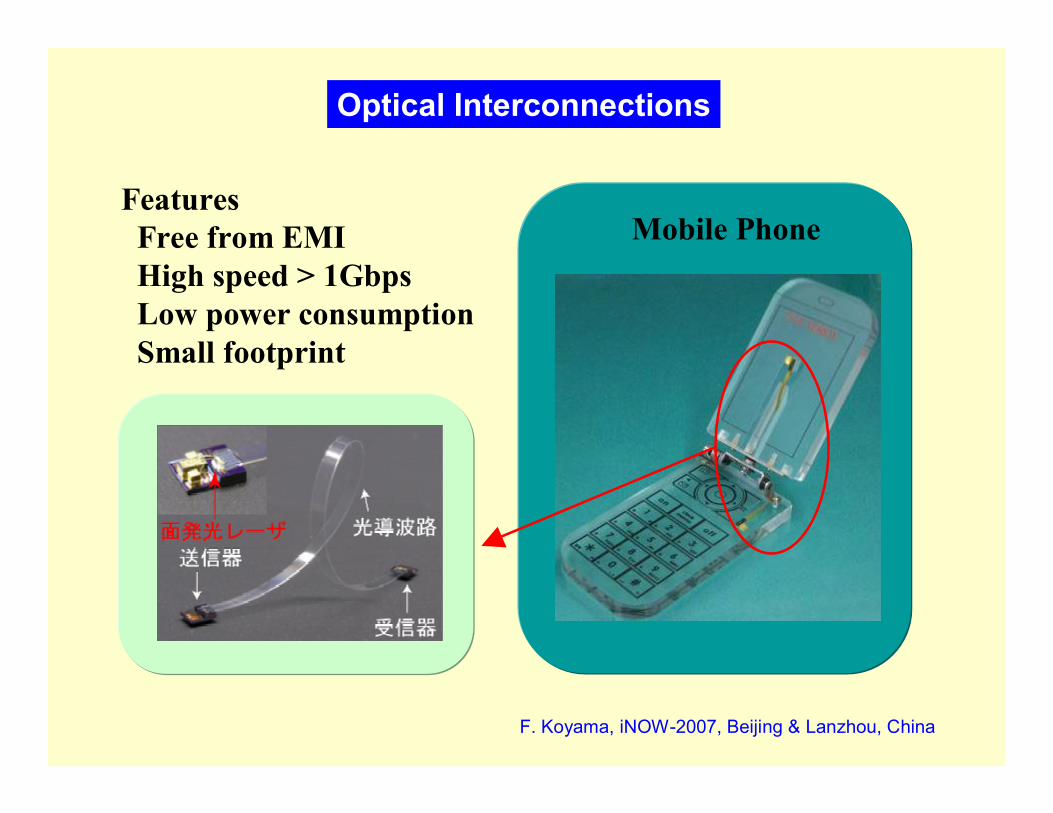
Mobile PhoneFeaturesFree from EMIHigh speed > 1GbpsLow power consumptionSmall footprint
Optical Interconnections
F. Koyama, iNOW-2007, Beijing & Lanzhou, China
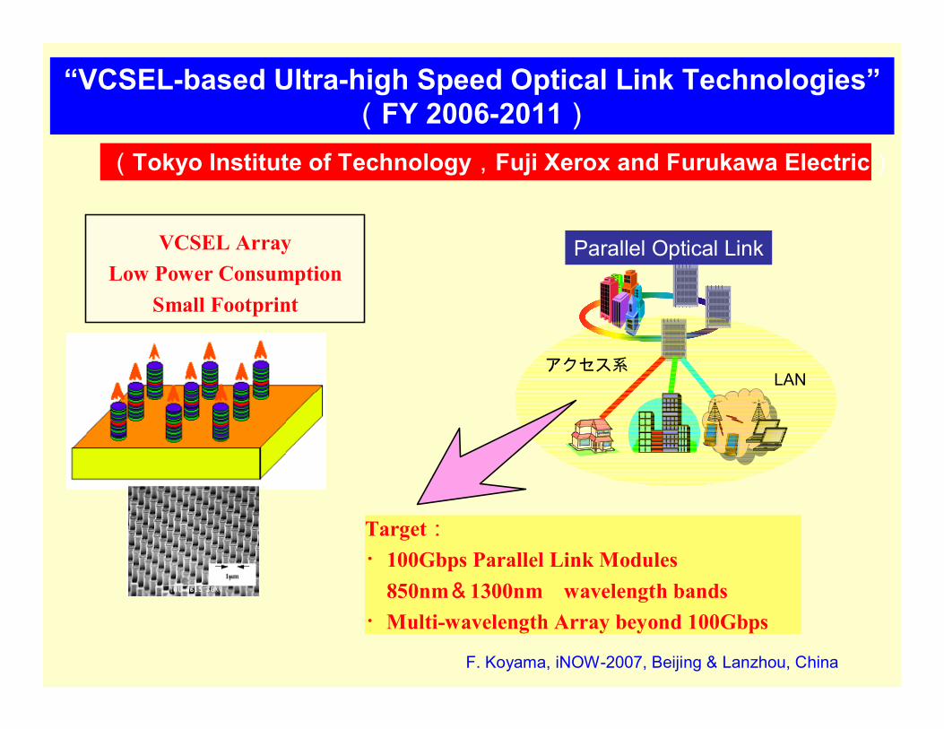
“VCSEL-based Ultra-high Speed Optical Link Technologies”(FY 2006-2011)
VCSEL ArrayLow Power Consumption
Small Footprint
Target:・100Gbps Parallel Link Modules 850nm&1300nm wavelength bands・Multi-wavelength Array beyond 100Gbps
(Tokyo Institute of Technology,Fuji Xerox and Furukawa Electric)
Parallel Optical Link
アクセス系LAN
F. Koyama, iNOW-2007, Beijing & Lanzhou, China
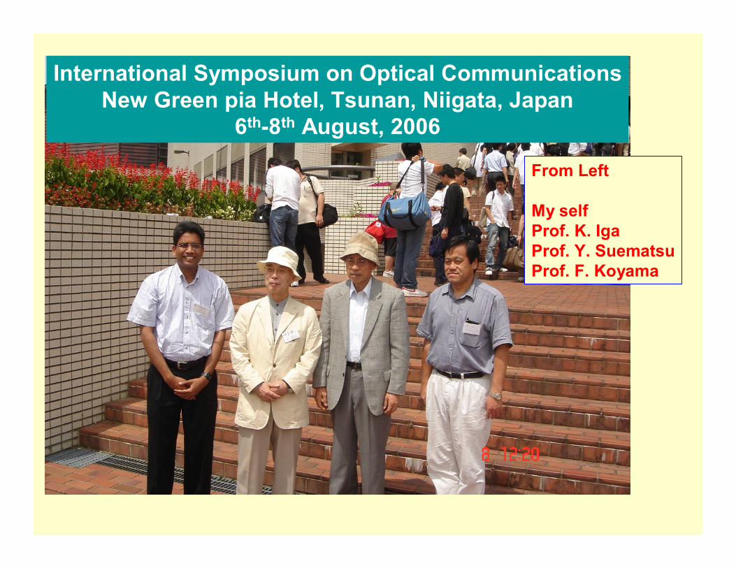
International Symposium on Optical CommunicationsNew Green pia Hotel, Tsunan, Niigata, Japan
6th-8th August, 2006
From Left
My selfProf. K. IgaProf. Y. SuematsuProf. F. Koyama
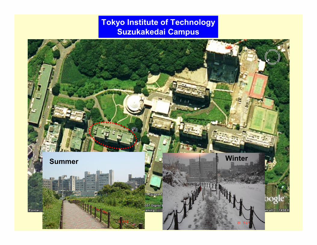
Tokyo Institute of TechnologySuzukakedai Campus
Summer Winter
Part-IIILeadership and Management
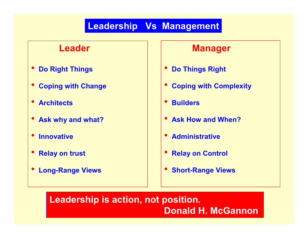
Leadership Vs Management
Leader
• Do Right Things
• Coping with Change
• Architects
• Ask why and what?
• Innovative
• Relay on trust
• Long-Range Views
Manager
• Do Things Right
• Coping with Complexity
• Builders
• Ask How and When?
• Administrative
• Relay on Control
• Short-Range Views
Leadership is action, not position.Donald H. McGannon
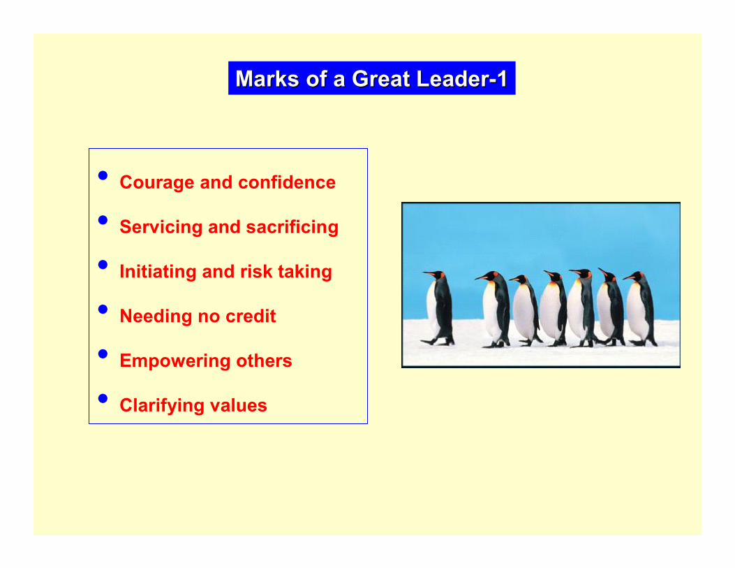
Marks of a Great LeaderMarks of a Great Leader--11
• Courage and confidence
• Servicing and sacrificing
• Initiating and risk taking
• Needing no credit
• Empowering others
• Clarifying values
• Honest, trustworthy
• Good role model
• Caring
• Committed
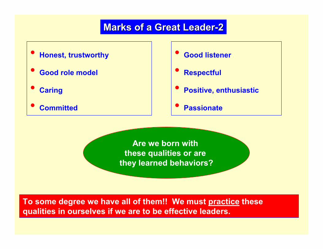
Marks of a Great LeaderMarks of a Great Leader--22
To some degree we have all of them!! We must practice these qualities in ourselves if we are to be effective leaders.
• Good listener
• Respectful
• Positive, enthusiastic
• Passionate
Are we born with these qualities or are
they learned behaviors?

The poor man is not he who is without a cent, but he who without a dream. Harry Kemp
http://www.main.nc.us/cartoons/Ihadadream.jpg
Do you have dream??
Scientist
Doctor
Manager
Leader
Teacher
Soldier
Engineer

Conclusions
• India in-brief : Unity in Diversity in the world !!
• Light emitting devices
• LED
• LASER
• Semiconductor LASER
• VCSEL & Optical Communication Applications
• Leadership !!
Acknowledgements
• JSPS, Science Dialogue staff
• Iwata Minami High School SD Organizers
• Prof. Kenichi Iga (JSPS)
• Prof. Fumio Koyama, (Tokyo Tech.)
• Mr. Satoshi Suda, (Tokyo Tech)
• All of you !!