Light Emission Properties of CVD Grown 2D monolayer WS2 ...
124
Light Emission Properties of CVD Grown 2D monolayer WS 2 for Optoelectronic Applications By M Bakhtiar Azim BSc in Materials & Metallurgical Engineering, BUET, 2017 Thesis Submitted in partial fulfillment of the requirements for the degree of Master of Applied Science in the School of Engineering Science Faculty of Applied Science Copyright © M Bakhtiar Azim SIMON FRASER UNIVERSITY 2020 Copyright in this work rests with the author. Please ensure that any reproduction or re-use is done in accordance with the relevant national copyright legislation.
Transcript of Light Emission Properties of CVD Grown 2D monolayer WS2 ...

Light Emission Properties of CVD Grown 2D monolayer WS2 for Optoelectronic Applications
By M Bakhtiar Azim
BSc in Materials & Metallurgical Engineering, BUET, 2017
Thesis Submitted in partial fulfillment of the
requirements for the degree of Master of Applied Science
in the
School of Engineering Science
Faculty of Applied Science
Copyright © M Bakhtiar Azim
SIMON FRASER UNIVERSITY
2020
Copyright in this work rests with the author. Please ensure that any reproduction
or re-use is done in accordance with the relevant national copyright legislation.

i
Approval
Name: M Bakhtiar Azim
Degree: Master of Applied Science
Title: Light Emission Properties of CVD Grown 2D monolayer WS2 for Optoelectronic Applications
Examining Committee: Chair: Michael Sjoerdsma
Senior Lecturer, School of Engineering Science
Michael M. Adachi Senior Supervisor, School of Engineering Science Assistant Professor _______________________________________
Bonnie Gray Supervisor, School of Engineering Science Professor
Ash Parameswaran Internal Examiner, School of Engineering Science Professor
_______________________________________
Date Defended/Approved:
[July 6th, 2020]

ii
Abstract
Two-dimensional Transitional Metal Dichalcogenides (TMDs) such as MX2 (M=
Mo, W; X= S, Se) have gained tremendous attention for use in optoelectronic
applications because of their high carrier mobility and indirect-direct band gap
transition for thin layers resulting in light emission. Moreover, monolayer TMDs
have exceptional other properties such as piezoelectricity, gate-induced
superconductivity, and tunable band structure. Mechanical exfoliation,
hydrothermal method, electrochemical exfoliation, chemical vapor deposition
(CVD) etc. are the most widely used methods for preparing monolayer TMDs.
Among these methods, CVD is regarded as the most promising approach because
it can produce large area crystal growth and uniform monolayers. The challenges
associated with other methods are either small flake size or low quality with lower
carrier mobility limiting performance in electronic devices. CVD grown TMDs tend
to show weak, non-uniform photoluminescence. If we want to use pristine TMDs
for optoelectectronics applications, we can use different chemical reagents such
as strong acid vapor for passivating surface of pristine TMDs which eventually
leads to enhanced photoluminescence. In this study, we first demonstrate growth
of monolayer triangular WS2 crystals using a 3-heating zone furnace using a
bottom-up CVD process. The average lateral crystal size is ~20-25 µm and the
largest crystal size is ~75 µm. Although, several research groups have reported
WS2 growth using WO3 and S precursors, specific parameters such as precursor
amount, growth substrate, growth pressure and flow rate, temperature, use of
gases (e.g. N2, Ar, Ar+H2), growth time, use of promoter (e.g. PTAS, NaCl, KBr),
pre-surface treatment of substrate etc. can vary widely from lab to lab, affecting
the growth morphology, mechanism, light emission, Raman spectra. Atomic Force
Microscopy (AFM) measurements indicate that the thickness of the monolayer
WS2 is ~1 nm. We also performed SEM imaging to investigate surface morphology
of monolayer WS2 and EDX to perform elemental analysis of monolayer WS2. X-
ray Photoelectron Spectroscopy (XPS) has been performed for pristine WS2 to
reveal its chemical states. Photoluminescence spectroscopy revealed a sharp

iii
emission peak at ~626 nm confirming indirect (bulk) to direct band-gap
(monolayer) transition in the monolayer. On the other hand, the PL intensity for
bi/tri-layer is relatively weak compared to monolayer. Moreover, we investigate the
effect of surface passivation using chemical reagents such as H2SO4-vapor for
modifying light emission property of pristine WS2 for using in next generation
optoelectronics. After H2SO4-vapor treatment, we achieved light emission at ~634
nm corresponding to red-shift with enhanced trion emission. Edges of H2SO4-
vapor treated sample shows enhanced biexciton compared to pristine-WS2. We
are able to achieve maximum 10-fold PL enhancement from our H2SO4-vapor
treated sample and, on an average, we got ~5 fold enhancement. H2SO4-vapor
treatment has not been used before for surface passivation. We also studied the
laser power dependence PL of pristine and H2SO4-vapor treated monolayer WS2
where it shows that with increasing laser power, pristine and H2SO4-vapor treated
monolayer WS2 shows enhanced PL specially at the crystal edges. In addition, we
also focused on investigating photoemission from pristine and H2SO4-vapor
treated monolayer WS2 along certain lines which eventually shows PL distribution
within a specific flake.
Keywords: TMDs; Optoelectronics; Laser Power; Photoluminescence; CVD;
WS2.

iv
Dedication
I would like to dedicate this thesis to my parents because of their
unconditional support!

v
Acknowledgements
After writing and editing all other parts, finally, I have started writing this
section. When I was writing Acknowledgement part, there were thousands of
things going through my mind. I have been recently diagnosed with a kidney tumor,
I don’t know whether it is benign or malignant, waiting for doing an MRI for last one
month which will decide the next step. It’s hard when someone has genuine heath
issue and simultaneously, he/she has to continue and focus on all other activities
overcoming all sorts of anxiety that is in my head for last four months. The effort I
put during this master’s is quite impossible to describe in just few words and I really
don’t want to drop without finishing it, all my efforts will go in vein. When I was
diagnosed with this health issue, I told myself, “I have to finish my thesis writing
somehow” that gave me courage to move forward day by day. With Almighty
Allah’s blessings and family support, I managed to gather all the data and
information that I believe makes this thesis complete.
Firstly, I would like to thank Almighty Allah to give me strength and patience
throughout these years to attain my goals for successful completion of graduate
studies. Then, I would like to express my gratitude towards my supervisor Dr.
Michael Adachi for his constant support and guidance and accepting me in his
group. I feel lucky and blessed to have a supervisor like him who is energetic,
helpful and caring at the same time. I was really motivated by my supervisor
because of his dedication and passion towards research. At the beginning, when I
started experimental works related to my thesis, I found it very difficult because as
a new group there was none to help except my supervisor. None had prior
experience related to my project that I was working on. I had a tough time initially
finding my way for appropriate research project. At one point due to my health
issues I thought that I wouldn’t be able to complete my studies. Now, because of
the blessings of Almighty Allah and moral support from my supervisor, I am writing
Acknowledgement after finishing other parts. During the second year of my MASc,
I spent quite a few months on experiments starting from purchasing equipments
and building up the measurement setup. We continued with experimental

vi
measurements taking lots of data. I was so excited when we observed expected
Chemical vapor Deposition (CVD) growth of monolayer WS2 after ~6 months’ hard
work, we performed more trial and error experiments and even organized a few
discussion sessions with lab mates and group members relating to this project. I
can also remember working in 4D Labs, LASIR for ~6-7 hours per day continuously
without any lunch break to get data on Photoluminescence. My supervisor always
motivated me with his usual encouraging smile. I made progress gradually
according to my supervisor’s suggestions and guidelines. I am out of words how
to express my gratitude towards my support system- my parents; without their
support, I won’t be here-living approx. 8000 miles away from home! I always feel
that the reason I am here because of the blessings of my parents.
I am also thankful to my lovely wife who is also doing her graduate studies
in Canada for motivating me towards my passion.
My lab colleagues who are MSc and PhD students helped me with growing
more samples and verifying the data again and again and suggested me what I
am supposed to try next. I would like to acknowledge CMC Microsystems, National
Sciences and Engineering Research Council of Canada (NSERC), Queen
Elizabeth Scholars, and Simon Fraser University (SFU). I am also grateful to Bud
Yarrow (BASc student, ENSC, SFU), Amin Abnavi (PhD student, ENSC, SFU),
Askar Abdelrahman (PhD student, ENSC, SFU), Thusani De Silva (MASc student,
ENSC, SFU) and Sofia Pineda (BASc student, Chemistry, SFU) for their valuable
suggestion and Professor Dr. Karen Kavanaugh (Physics, SFU) and Mirette Fawzy
(PhD student, Physics, SFU) for their help in performing TEM characterization. I
am also thankful to Dr. Saeid Kamal (LASIR), Dennis Hsiao, Rana Faryad Ali (PhD
student, Chemistry, SFU) and 4D LABS, SFU for providing constant support,
valuable suggestion and giving excess for using their facilities to successfully
complete the project. At the end, I want to thank from the bottom of my heart to all
the people that support and accompany me during my graduate studies at SFU.

vii
Table of Contents
Approval ........................................................................................................................... i
Abstract ........................................................................................................................... ii
Dedication ...................................................................................................................... iv
Acknowledgements ....................................................................................................... v
List of Figures................................................................................................................. ix
List of Tables ................................................................................................................ xiv
List of Acronyms ............................................................................................................ xv
Chapter 1: Introduction ................................................................................................. 1
1.1. Opportunities Beyond Silicon ................................................................................ 1
1.2. Project Goal .......................................................................................................... 1
1.3. Motivation of Thesis .............................................................................................. 2
1.4. The Structure of Thesis ........................................................................................ 3
Chapter 2: Background & Literature Review of 2D Materials ..................................... 4
2.1. Discovery of 2D Materials ..................................................................................... 4
2.2. Fundamentals of Semiconductor Materials ........................................................... 5
2.2.1. Electron, Hole and Exciton ................................................................................. 5
2.2.2. Direct and Indirect bandgap ........................................................................... 7
2.2.3. Carrier Recombination and Photoluminescence (PL) ......................................... 7
2.3. Crystal Lattice Band Structure .............................................................................. 9
2.4. Properties of TMDs ................................................................................................ 10
2.4.1. Electrical and Electronic Properties .................................................................. 11
2.4.2. Thermal Properties .......................................................................................... 12
2.4.3. Chemical Properties ......................................................................................... 12
2.4.4. Mechanical Properties ..................................................................................... 13
2.4.5. Young`s Modulus ............................................................................................. 13
2.4.6. Light-Emitting properties of 2D TMDs .............................................................. 14
2.5. Generation of Defects in 2D TMDs ..................................................................... 15
Chapter 3: Background & Literature Review of CVD growth of 2D monolayer, Characterization & PL Enhancement ......................................................................... 16
3.1. Production Methods of 2D TMDs Crystals .......................................................... 17
3.1.1. Exfoliation ....................................................................................................... 17
3.2. Overview of Characterization Methods of CVD Grown Monolayer WS2 .................. 27
3.2.1. Optical Imaging ................................................................................................ 28
3.2.2. Scanning Electron Microscopy (SEM) and Energy Dispersive Spectroscopy (EDS) ......................................................................................................................... 28
3.2.3. Transmission Electron Microscopy (TEM) ........................................................ 29
3.2.4. Raman Spectroscopy ....................................................................................... 29
3.2.5. Atomic Force Microscopy (AFM) ...................................................................... 32
3.2.6. X-ray Photoelectron Spectroscopy (XPS)......................................................... 33
3.2.7. Photoluminescence (PL) .................................................................................. 35

viii
3.3. Overview of PL Enhancement based on Literature ................................................. 37
Chapter 4: Experimental Details ................................................................................. 57
4.1. Materials................................................................................................................. 57
4.2. Experiment ............................................................................................................. 58
4.2.1. CVD Growth of monolayer WS2 on SiO2/Si substrate ....................................... 58
4.3. Experimental Results & Discussions ...................................................................... 64
4.3.1. Optical ............................................................................................................. 64
4.3.2. SEM &EDS ...................................................................................................... 66
4.3.3. TEM ................................................................................................................. 67
4.3.4. Raman Spectroscopy ....................................................................................... 68
4.3.5. AFM ................................................................................................................. 70
4.3.6. XPS ................................................................................................................. 71
4.3.7. PL .................................................................................................................... 73
Chapter 5: PL Enhancement of Monolayer WS2 ........................................................ 84
5.1. Purpose of PL Enhancement .................................................................................. 84
5.2. Methodology ........................................................................................................... 85
5.3. Results and Discussion .......................................................................................... 86
5.3.1. PL Enhancement of H2SO4-Vapor Treated Monolayer WS2 ............................. 86
5.3.2. Room Temperature Laser Power Dependent PL of H2SO4-Vapor Treated monolayer WS2 .......................................................................................................... 91
5.3.4. XPS Study of H2SO4- Vapor Treated Monolayer WS2 ...................................... 96
Chapter 6: Future Projects & Conclusion .................................................................. 99
6.1. Limitation ................................................................................................................ 99
6.2. Contribution ............................................................................................................ 99
6.3. Future Work ........................................................................................................... 99
6.4. Conclusion ........................................................................................................... 100
Bibliography ................................................................................................................ 100
Appendix A. ............................................................................................................... 106

ix
List of Figures
Figure 1: Amplitude AFM images showing shape evolutions of CVD-grown WSe2 flakes at different growth temperatures of (a) 900⁰C, (b) 950⁰C, (c and d) 1025⁰C, (e and f) 1050⁰C. Unusual, non-triangle shapes are gradually found as the growth temperature increases. (a and b) Monolayer triangles with different sizes; (c and d) thin few layer truncated triangle and hexagon with curve edges; (e and f) thick few layer triangle and hexagon with straight edges. Reprinted (adapted) with permission from Liu, B., Fathi, M., Chen, L., Abbas, A., Ma, Y., & Zhou, C. (2015). Chemical vapor deposition growth of monolayer WSe2 with tunable device characteristics and growth mechanism study. ACS Nano, 9(6), 6119–6127. Copyright 2015) American Chemical Society.......................................................... 21
Figure 2: Effect of growth temperatures on the sizes and layer numbers of CVD-grown WSe2. Optical microscopy images of WSe2 flakes grown at (a) 850⁰C, (b) 900⁰C, and (c) 1050⁰C. The growth durations are 15 min for all cases. (d) The correlation of average WSe2 flake sizes and layer numbers with growth temperatures. The vertical error bars indicate standard deviations of the flake sizes in statistical analysis. Reprinted (adapted) with permission from Liu, B., Fathi, M., Chen, L., Abbas, A., Ma, Y., & Zhou, C. (2015). Chemical vapor deposition growth of monolayer WSe2 with tunable device characteristics and growth mechanism study. ACS Nano, 9(6), 6119–6127. Copyright (2015) American Chemical Society. ........... 21
Figure 3: Effect of growth durations on the sizes of CVD-grown monolayer WSe2. Optical microscopy images of WSe2 grown for (a) 1 min, (b) 5 min, and (c) 5 h. The growth temperatures are 950⁰C for all cases. (d) Plot of average flake sizes versus growth durations of 1 min, 3 min, 5 min, 10 min, 15 min, 30 min, 60 min, and 5 h. The vertical error bars are standard deviations in statistical analysis. Reprinted (adapted) with permission from Liu, B., Fathi, M., Chen, L., Abbas, A., Ma, Y., & Zhou, C. (2015). Chemical vapor deposition growth of monolayer WSe2 with tunable device characteristics and growth mechanism study. ACS Nano, 9(6), 6119–6127. Copyright 2015) American Chemical Society.......................................................... 22
Figure 4: Shape Evolution of CVD WSe2 with increased Temperature. Reprinted (adapted) with permission from Liu, B., Fathi, M., Chen, L., Abbas, A., Ma, Y., & Zhou, C. (2015). Chemical vapor deposition growth of monolayer WSe2 with tunable device characteristics and growth mechanism study. ACS Nano, 9(6), 6119–6127. Copyright 2015) American Chemical Society. .................................................................. 23
Figure 6:Raman Spectra at different excitation wavelength (a) 488 nm, (b) 514 nm, (c) 647 nm. Reprinted (adapted) with permission from Berkdemir, A., Gutiérrez, H. R., Botello-Méndez, A. R., Perea-López, N., Elías, A. L., Chia, C.-I., Wang, B., Crespi, V. H., López-Urías, F., & Charlier, J.-C. (2013). Identification of individual and few layers of WS 2 using Raman spectroscopy. Scientific Reports, 3(1), 1–8. Copyright © 2013, Springer Nature. ................................................................................................... 31
Figure 7: (a) Peak Frequency vs Number of Layers, (b) Intensity ratio vs Number of Layers[73]. Reprinted (adapted) with permission from Berkdemir, A.,

x
Gutiérrez, H. R., Botello-Méndez, A. R., Perea-López, N., Elías, A. L., Chia, C.-I., Wang, B., Crespi, V. H., López-Urías, F., & Charlier, J.-C. (2013). Identification of individual and few layers of WS2 using Raman spectroscopy. Scientific Reports, 3(1), 1–8. Copyright © 2013, Springer Nature. ................................................................................................... 32
Figure 8: Absorption and related radiative and non-radiative processes involved during the whole procedure of Photoluminescence. .......................................... 36
Figure 9: (a) Raman spectra and (b) Raman intensity maps of a monolayer MoSe2 flake before and after HBr treatment. Reprinted (adapted) with permission from Han, H.-V., Lu, A.-Y., Lu, L.-S., Huang, J.-K., Li, H., Hsu, C.-L., Lin, Y.-C., Chiu, M.-H., Suenaga, K., & Chu, C.-W. (2016). Photoluminescence enhancement and structure repairing of monolayer MoSe2 by hydrohalic acid treatment. ACS Nano, 10(1), 1454–1461. Copyright (2016), American Chemical Society. .................................................................. 41
Figure 10: (a) PL intensity mappings of an individual MoSe2 flake before and after HBr treatment. Profiles in (b) and (c) show the PL intensity and photon energy modulation as a function of surface location along the solid line indicated in (a) Reprinted (adapted) with permission from Han, H.-V., Lu, A.-Y., Lu, L.-S., Huang, J.-K., Li, H., Hsu, C.-L., Lin, Y.-C., Chiu, M.-H., Suenaga, K., & Chu, C.-W. (2016). Photoluminescence enhancement and structure repairing of monolayer MoSe2 by hydrohalic acid treatment. ACS Nano, 10(1), 1454–1461. Copyright (2016), American Chemical Society.......... 42
Figure 11: (a) Photoluminescence of the as-grown and HBr-treated monolayer MoSe2 at 10 K. (b) Temperature dependence of PL for the MoSe2 after HBr treatment. (c) Trion and exciton peak energies. (d) Intensity of trion to exciton peak as a function of temperature. Reprinted (adapted) with permission from Han, H.-V., Lu, A.-Y., Lu, L.-S., Huang, J.-K., Li, H., Hsu, C.-L., Lin, Y.-C., Chiu, M.-H., Suenaga, K., & Chu, C.-W. (2016). Photoluminescence enhancement and structure repairing of monolayer MoSe2 by hydrohalic acid treatment. ACS Nano, 10(1), 1454–1461. Copyright (2016), American Chemical Society. ...................................... 43
Figure 12: (a) Optical images of as-prepared 1L-, 2L-, and 3L-MoS2 on SiO2/Si substrates. (b) Raman spectra of the as-prepared 1L-, 2L-, and 3L-MoS2
measured at room temperature. (c) PL spectra of the as prepared 1L-, 2L-, and 3L-MoS2. The PL peak due to the indirect band gap transition is denoted as I, and those due to the direct band gap transition are denoted as peaks A and B[36](Mouri et al., 2013). Reprinted (adapted) with permission from Mouri, S., Miyauchi, Y., & Matsuda, K. (2013). Tunable photoluminescence of monolayer MoS2 via chemical doping. Nano Letters, 13(12), 5944–5948. Copyright (2016) American Chemical Society ............................................................................................................... 46
Figure 13: (a) PL spectra of 1L-MoS2 before and after F4TCNQ doping. (b) PL spectra of 1L-MoS2 obtained at each doping step (0, 1, 2, 4, 6, 10, 13, and 16 steps). The inset shows the normalized PL spectra of 1L-MoS2 at each doping step. (c) Analysis of the PL spectral shapes for as-prepared and F4TCNQ-doped 1L-MoS2. The A peaks in the PL spectra were reproduced by assuming two peaks with Lorentzian functions, corresponding to the trion (X−) and the exciton (X) peaks, were overlapped. (d) Integrated PL intensity of the negative trion Ix−, exciton Ix,

xi
and the sum (Itotal) of Ix and Ix−as functions of the number of F4TCNQ doping steps. Solid lines show the calculated PL intensity curves calculated by solving the rate equations in the three-level model. Reprinted (adapted) with permission from Mouri, S., Miyauchi, Y., & Matsuda, K. (2013). Tunable photoluminescence of monolayer MoS2 via chemical doping. Nano Letters, 13(12), 5944–5948. Copyright (2013) American Chemical Society. .................................................................. 47
Figure 14: (a) PL spectra of 1L-MoS2 before and after being doped with p-type molecules (TCNQ and F4TCNQ). (b) PL spectra of 1L-MoS2 before and after being doped with an n-type dopant (NADH). Reprinted (adapted) with permission from Mouri, S., Miyauchi, Y., & Matsuda, K. (2013). Tunable photoluminescence of monolayer MoS2 via chemical doping. Nano Letters, 13(12), 5944–5948. Copyright (2013) American Chemical Society ................................................................................................... 48
Figure 15: PL spectra for both the as-exfoliated and TFSI treated (a) WS2, (b) MoS2, (c) WSe2, and (d) MoSe2 monolayers measured at an incident power density of 1 × 10⁻² Wcm−2. The inset shows normalized spectra for each material. Absorption spectra of both as-exfoliated (dashed lines) and chemically treated (solid lines) WS2, MoS2, WSe2, and MoSe2 monolayers (e). Reprinted (adapted) with permission from Amani, M., Taheri, P., Addou, R., Ahn, G. H., Kiriya, D., Lien, D.-H., Ager III, J. W., Wallace, R. M., & Javey, A. (2016). Recombination kinetics and effects of superacid treatment in sulfur-and selenium-based transition metal dichalcogenides. Nano Letters, 16(4), 2786–2791. Copyright (2016) American Chemical Society. .................................................................................................. 51
Figure 16: Radiative decay of as-exfoliated (a) and chemically treated (b) WS2 at various initial carrier concentrations (n0) as well as the instrument response function (IRF). Reprinted (adapted) with permission from Amani, M., Taheri, P., Addou, R., Ahn, G. H., Kiriya, D., Lien, D.-H., Ager III, J. W., Wallace, R. M., & Javey, A. (2016). Recombination kinetics and effects of superacid treatment in sulfur-and selenium-based transition metal dichalcogenides. Nano Letters, 16(4), 2786–2791. Copyright (2016) American Chemical Society. .................................................................. 51
Figure 17: (a) Configuration of the growth setup utilized to prepare the MoS2 samples for this study. The temperature of the substrate and molybdenum precursor (in the furnace hot zone) and the sulfur precursor (surrounded by heating tape) is controlled and measured independently. (b and c) Schematic illustrating the two primary sample preparation routes investigated in this study. As-grown MoS2 triangular domains and films, which show tensile strain after growth were either (b) treated by TFSI directly, resulting in a small reduction in the PL QY, or (c) transferred from the growth substrate using a PMMA-mediated transfer process, releasing the strain, and subsequently treated by TFSI, resulting in a final PL QY of approximately 30%. Reprinted (adapted) with permission from Amani, M., Burke, R. A., Ji, X., Zhao, P., Lien, D.-H., Taheri, P., Ahn, G. H., Kirya, D., Ager III, J. W., & Yablonovitch, E. (2016). High luminescence efficiency in MoS2 grown by chemical vapor deposition. ACS Nano, 10(7), 6535–6541. Copyright (2016) American Chemical Society. ....................................... 52

xii
Figure 18: (a) Raman spectra measured on as-grown and transferred MoS2 single domains. (b) PL spectra of the MoS2 single domains measured before and after transfer at a laser power of 50 W/cm2. Reprinted (adapted) with permission from Amani, M., Burke, R. A., Ji, X., Zhao, P., Lien, D.-H., Taheri, P., Ahn, G. H., Kirya, D., Ager III, J. W., & Yablonovitch, E. (2016). High luminescence efficiency in MoS2 grown by chemical vapor deposition. ACS Nano, 10(7), 6535–6541. Copyright (2016) American Chemical Society. .................................................................................. 53
Figure 19: (a) Raman spectra measured on transferred MoS2 single domains before and after treatment by TFSI. (b) PL spectra obtained at a pump power of 0.1 W/cm2 for transferred MoS2 single domains both before and after chemical treatment by TFSI. (c) Radiative decay of transferred MoS2 single domains obtained at a pump fluence of 5 × 10⁻²μJ/cm2 both before and after chemical treatment by TFSI, as well as the instrument response function (IRF). Reprinted (adapted) with permission from Amani, M., Burke, R. A., Ji, X., Zhao, P., Lien, D.-H., Taheri, P., Ahn, G. H., Kirya, D., Ager III, J. W., & Yablonovitch, E. (2016). High luminescence efficiency in MoS2 grown by chemical vapor deposition. ACS Nano, 10(7), 6535–6541. Copyright (2016) American Chemical Society. ............................. 53
Figure 20: (a) Optical image of a transferred MoS2 single domain and log-scale luminescence images from the same area obtained (b) before and (c) after chemical treatment by TFSI. (d) Optical image of a transferred continuous MoS2 film and log scale luminescence images from the same area obtained (e) before and (f) after chemical treatment by TFSI[84]. Reprinted (adapted) with permission from Amani, M., Burke, R. A., Ji, X., Zhao, P., Lien, D.-H., Taheri, P., Ahn, G. H., Kirya, D., Ager III, J. W., & Yablonovitch, E. (2016). High luminescence efficiency in MoS2 grown by chemical vapor deposition. ACS Nano, 10(7), 6535–6541. Copyright (2016) American Chemical Society. ....................................................... 54
Figure 21: (a) CVD Setup in the ENSC Cleanroom, (b) Image representing reaction at High Temperature in CVD Furnace ........................................................ 58
Figure 22: Schematic of Small Quartz Tube and Boat/Holder ........................................ 58
Figure 23: (a) Schematic Experimental Set-Up of CVD growth, (b) 3D view of CVD Growth of monolayer WS2 on SiO2/Si ..................................................... 61
Figure 24: Temperature profile as a function of Time for CVD growth of monolayer WS2
............................................................................................................... 61
Figure 25: (a) and (b) Monolayer WS2 on SiO2/Si substrate (c) and (d) Multilayer WS2 on SiO2/Si substrate .................................................................................... 65
Figure 26: (a) Optical Image under Bright Field where monolayer is visible and (b) Optical Image under Dark Field where monolayer is not visible .............. 66
Figure 27: SEM of CVD grown Pristine monolayer WS2 ................................................ 67
Figure 28: EDS of Pristine monolayer WS2 (a) before CVD deposition and (b) after CVD deposition............................................................................................... 67
Figure 29: TEM of Pristine monolayer WS2 directly grown on TEM grids (a) TEM Image and (b) SAED Pattern ............................................................................ 68
Figure 30: (a) Raman Spectra of monolayer WS2, (b) Intensity ratio vs Number of layers ............................................................................................................... 69

xiii
Figure 31: (a) AFM mapping of monolayer WS2 (b) Height profile along Blue Line, ....... 71
Figure 32: XPS Spectra of monolayer WS2 (a) S 2p, (b) Core level W 4f ...................... 73
Figure 33: (a,b) Fluorescence Images of monolayer WS2, (c) PL intensity map of pristine monolayer WS2, (d) 2D surface plot of Pristine WS2, (e) 3D Surface Plot of Pristine WS2and (f) PL spectra of grown monolayer WS2 ................... 76
Figure 34: (a) Laser Power Dependent PL study of Pristine WS2 in terms of Wavelength (nm) and (b) Laser Power Dependent PL study of Pristine WS2 in terms of Photon Energy (eV) ................................................................................ 79
Figure 35: PL Intensity variation with Laser Power in log scale ..................................... 79
Figure 36: PL Intensity variation along line with distance (a) PL Image of Pristine WS2 with Line 1, (b) PL variation along Line 1, (c) PL Image of Pristine WS2 with Line 2, (d) PL variation along Line 2, (e) PL Image of Pristine WS2 with Line 3, (f) PL variation along Line 3, (g) PL Image of Pristine WS2 with Line 4, (h) PL variation along Line 4, (i) PL Image of Pristine WS2 with Line 5, (j) PL variation along Line 5 and (k) PL Image of Pristine WS2
with Line 6, (l) PL variation along Line 6 ................................................. 82
Figure 37: (a) Setup of H2SO4 Vapor Treatment in Yellow Room, (b) Schematic Setup of H2SO4-Vapor Treatment ......................................................................... 86
Figure 38: PL Intensity mapping of Pristine-WS2 (a) before and (b) after H2SO4-vapor Treatment............................................................................................... 89
Figure 39: PL Intensity vs Wavelength (nm) before and after H2SO4-vapor treatment ... 90
Figure 40: Normalized PL Intensity vs Wavelength (nm) before and after H2SO4-vapor treatment ................................................................................................ 90
Figure 41: (a) Laser Power Dependent PL study of H2SO4-Vapor Treated Monolayer WS2 in terms of Wavelength (nm) and (b) Laser Power Dependent PL study of H2SO4-Vapor Treated Monolayer WS2 in terms of Photon Energy (eV) ........................................................................................................ 93
Figure 42: PL Intensity variation with Laser Power in log scale ..................................... 93
Figure 43: PL Intensity variation along certain line (a) PL Image of H2SO4-Vapor Treated Monolayer WS2 with Line 1, (b) PL variation along Line 1, (c) PL Image of H2SO4-Vapor Treated Monolayer WS2 with Line 2, (d) PL variation along Line 2, (e) PL Image of H2SO4-Vapor Treated Monolayer WS2 with Line 3, (f) PL variation along Line 3, (g) PL Image of H2SO4-Vapor Treated Monolayer WS2 with Line 4, (h) PL variation along Line 4, (i) PL Image of H2SO4-Vapor Treated Monolayer WS2 with Line 5, (j) PL variation along Line 5 and (k) PL Image of H2SO4-Vapor Treated Monolayer WS2 with Line 6, (l) PL variation along Line 6 ........................................................ 96
Figure 44: XPS Spectra of monolayer WS2 before and after H2SO4 vapor treatment (a) S 2p and (b) Core Level W 4f .................................................................... 98

xiv
List of Tables
Table 1: CVD process parameters for monolayer WS2 growth……………………………93

xv
List of Acronyms
CVD Chemical Vapor Deposition
WS2 Tungsten Disulphide
TMDs Transitional Metal Dichalcogenides
RT Room Temperature
LT Low Temperature
PL Photoluminescence
SEM Scanning Electron Microscopy
EDS Energy Dispersive Spectroscopy
TEM Transmission Electron Microscopy
AFM Atomic Force Microscopy
XPS X-ray Photoelectron Microscopy

1
Chapter 1: Introduction
1.1. Opportunities Beyond Silicon
Two-dimensional (2D) materials are a class of materials possessing
ultimate limit of thinness in vertical dimension and representing the thinnest
artificial materials in the universe, have demonstrated potential for discovering
interesting phenomena in condensed matter physics and as a promising platform
to push the frontier of semiconductor technology beyond the Moore’s law. When I
was taking a course “ENSC 893: Principles of Nanoengineering” in 1st year of my
masters, I got to know about Richard Feynman who raised up this question in his
famous lecture in 1959 “What could we do with layered structures with just the right
layers?”, “There’s plenty of room at the bottom”. Among these ‘right’ layers, 2D
materials at atomic scale are particularly interesting and have attracted lots of
attention in recent years.
1.2. Project Goal
The master’s project aims to achieve room temperature (RT) enhanced light
emission from pristine-WS2 using surface passivation. At first, monolayer WS2 was
deposited on SiO2/Si substrate using Chemical Vapor Deposition (CVD) and
different characterizations such as Raman, Photoluminescence (PL), Atomic
Force Microscopy (AFM), X-ray Photoelectron Spectroscopy (XPS), Transmission
Electron Microscopy (TEM), Scanning Electron Microscopy (SEM) and Energy
Dispersive Spectroscopy (EDS) of pristine-WS2 have been performed. Finally, PL
enhancement study has been performed using 50 ml 2.24 M H2SO4-Vapor
treatment for pristine-WS2 which has been done for the first time to achieve room
temperature enhanced light emission. In the field of photoluminescence, this is
new advancement regarding surface passivation with H2SO4-vapor treatment
which shows maximum 10-fold enhancement at room temperature. Surface
passivation supposed to passivate the point defects and surface vacancy/Sulphur

2
vacancy which ultimately reduces the non-radiative recombination sites and show
enhanced exciton peak. Suppression of Phonons usually takes place significantly
at Low Temperature (LT) and hence enhanced PL is observed at 77K or below for
2DTMDs, but we performed experiment at Room Temperature (RT); carriers at RT
can have enough energy to get to non-radiative recombination centers, so, in
general, a strong reduction of the intensity of the PL signal is observed which is
not seen in our samples at RT; excitonic effects are more efficient at LT but for our
samples exciton peak is sharp at RT-for pristine-WS2 and H2SO4-vapor treated
WS2. Most of the optoelectronics operating temperature is ~298k not 77k;
therefore, it is important to focus on achieving enhanced PL at RT. Furthermore,
laser power dependent PL, variation of PL of pristine-WS2 and H2SO4-vapor
treated WS2 along certain lines has been studied as well.
1.3. Motivation of Thesis
In 2004, two scientist Novoselov and Geim experimentally found unique
properties of 2D material ‘Graphene’ which was exfoliated using scotch-tape
method at University of Manchester. Although Graphene shows impressive
properties such as, but it has one limiting factor which is zero-band gap. Then,
researchers and scientists started to explore other 2D materials such as TMDs (i.e.
MoS2 ,WS2). TMDs show indirect to direct band gap transition and has wide band
gap which make them potential candidate for optoelectronic applications. The
weak van der wall force between each layer of TMDs enables tuning of properties.
Researchers and Scientists are working day and night to figure out why the
pristine-TMDs show weak, non-uniform PL and how they can enhance it. So far,
different chemical reagents have been used such as acetone, p-type and n-type
dopants, TFSI, HI etc. and still more work is needed.

3
1.4. The Structure of Thesis
This thesis includes the research findings over the time span of two years
of Master’s degree at the Department of Engineering Science, Simon Fraser
University.
It starts with a literature review in Chapter 2 that provides an overview of
Discovery of 2D materials, Fundamentals of Semiconductor Materials, Crystal
Lattice Band Structure, Properties of 2D TMDs, Structural Defects in 2D TMDs.
Chapter 3 covers the overview of 2D TMDs production, overview of
characterization techniques and Literature Review of Photoluminescence
Enhancement of TMDs.
Chapter 4 summarizes my work on CVD growth of monolayer WS2 and
different characterization techniques, Room Temperature PL of Pristine WS2,
Room Temperature Laser Power Dependent PL of Pristine WS2, Room
Temperature PL Variation of Pristine WS2 along certain lines that have been
performed throughout these 2 years.
Chapter 5 shows Purpose of PL Enhancement, Methodology, PL
Enhancement of H2SO4 Vapor Treated Monolayer WS2, PL dependence on Laser
Power, Room Temperature Laser Power Dependent PL of H2SO4-Vapor Treated
monolayer WS2, Room Temperature PL Variation of H2SO4-Vapor Treated WS2
along certain lines.
Chapter 6 includes the other experimental works that have been done
simultaneously during this 2 years, future work and conclusion of the thesis finally.

4
Chapter 2: Background & Literature Review of 2D Materials
Chapter 2 discusses about fundamental concepts such as exciton, trion,
biexciton, carrier recombination, indirect and direct band gap, quantum yield (QY),
light emission depending on TMDs crystal structure, role of defects in a crystal that
are very important for understanding 2D based semiconductors properties.
Fundamental concepts help to explain results properly that are being achieved in
this thesis and without clear explanation the goal of this thesis will not be achieved.
Chapter 2 focuses on 2D Materials’ Discovery, Fundamentals of Semiconductors,
TMDs Crystal Band Structure, TMDs Properties, and Defects in TMDs.
2.1. Discovery of 2D Materials
Although it has been studied for long time as a theoretical model [1]–[6],
atomically thick 2D crystals such as graphene was predicted to not exist because
of thermodynamic instability [7] and was described as pure ‘academic’ material.
However, people’s perception changed in 2004 when graphene was isolated by
scotch-tape method from graphite in the lab[8]–[10]. The discovery of graphene
not only brought Andre Geim and Konstantin Novoselov the 2010 Nobel prize in
physics, it also opened the door to an exciting world of 2D materials.
When thinned down to atomic layer, graphene shows quite different and
distinguished characteristics compared to graphite, it even got a nickname of
‘miracle material’ due to its superior properties. In terms of applied science, the
amazing characteristics graphene possesses rise up new opportunities for a wide
range of applications. These includes but not are not limited to optical absorption
of exactly πα = 2.3% (α is the fine structure constant), super-high intrinsic strength,
ultrahigh thermal conductivity, amazing room-temperature electron mobility etc.
Graphene has shown its potential to be used in various areas, such as flexible
electronics, photonics, energy generation and storage, sensors, bio applications,
paints and coating and so on [11]–[13]. It is almost impossible to mention all the

5
potential applications and new physical phenomena graphene has brought to us.
This atomically thin material has been an obsession for researchers around the
world since its birth in the lab and new things are still coming out every day.
On the other hand, the message we could take from graphene is that the
2D materials have extraordinary properties compared to their bulk forms and hold
huge potential for lots of applications, which is not fully explored at all. This inspired
people to start looking for other graphene-like materials, such as boron nitride
(hBN), transition metal dichalcogenides (TMDs), black phorsphone, silicene and
germanene. TMDs are semiconductors and have shown many superior properties
for applications in photonics. In this thesis, we will focus on TMDs. To better serve
for our topics, we start reviewing some basic concepts in semiconductor materials
in the following section.
2.2. Fundamentals of Semiconductor Materials
The core of electronic technology is to control the flow of electrons and
photonics is the technology to control the flow of photons. Semiconductor
optoelectronics connect these two technologies: photons create mobile charge
carriers and charge carriers in turn control the flow of photons. Semiconductor
based optoelectronic devices such as laser, light-emitting diodes (LED) have
changed our life a lot and this field is still moving on quickly. Thus, studying optical
properties of semiconductors, which is in the domain of semiconductor optics, is
essential for fabricating advanced optoelectronic devices[14].
2.2.1. Electron, Hole and Exciton
Semiconductor is a crystalline or amorphous solid with electrical
conductivity between conductor and insulator, typical examples include Si and
GaAs. The conductivity of semiconductors could be altered by changing the
temperature, doping with carriers or illumination with light. Atoms consisting of
solid-state semiconductor could not be treated as single entity like hydrogen
atoms, because they interact strongly with other nearby atoms. Thus, the

6
conduction electrons in semiconductor are not bound to single atom, they
collectively belong to all atoms as a whole. In addition, atoms in lattice structure
apply periodic potential on the electrons, the solutions to the Schr¨odinger
equations for the electron energy form energy bands. In each band, a great deal
of discrete energy levels are densely packed together, which could be well
approximated as continuum. The conduction and valence band are separated by
a bandgap energy Eg. The bandgap energy is an important parameter when
describing the electronic and optical properties of materials, and the value depends
on material. For example, the Eg is 1.2 and 1.42 eV (electron volts) for Si and
GaAs at room temperature, respectively[14].
The electrons in the semiconductor obey the Pauli exclusion principle, this
principle says that two or more electrons could not occupy the same quantum state
and electrons fill up the lowest available energy level first. At absolute zero
temperature, the valence band is fully occupied while the conduction band is
empty, thus material is not conductive at all. However, with increasing temperature,
some electrons will be thermally excited to transit from valence band onto
conduction band leaving behind some unoccupied quantum states called holes.
The electrons in the conduction bands act as mobile carriers and the unoccupied
states in valence band allow other electrons to exchange places with applied
electric field. Thus, the holes left in the valence band could be regarded as carriers
with positive charge. The overall effect is that every electron excitation creates
mobile carriers in both conduction and valence bands, free electron and hole,
respectively. The conductivity of semiconductor materials increases sharply with
temperature as more and more charge carriers are generated[14].
Under certain excitation condition such as light illumination, exciton might
be formed. Exciton is a bound electron-hole pair, the electron and hole interact
with each other through Coulomb forces, similar to hydrogen atoms. There are two
basic types of excitons, free excitons and tightly bound excitons. The free excitons
have large radius and are delocalized states, thus they can move freely throughout
crystal. In contrast, tightly bound excitons have small radius and are bound to
specific atom or molecule. Excitons can only exist in stable form when their

7
attractive potential is large enough to protect them from collisions with phonons,
the energy of these bound states is called binding energy. Excitons play an
important role in determining the electronic and optical properties of
semiconductors, especially for low dimensional ones [15].Other hybrid particle
such as trion (bound states of two electrons and one hole, or one electron and two
holes) or biexciton (bound states of two exciton) might be formed as well in some
semiconductor systems[14].
2.2.2. Direct and Indirect bandgap
Based on the band structure, semiconductor materials could be categorized
into two groups: direct- and indirect-bandgap materials. Direct-bandgap materials
refer to semiconductors that have the same wave number k (momentum) for the
conduction-band minimum and the valence-band maximum energy. Materials that
do not satisfy this condition are indirect bandgap. GaAs has indirect bandgap while
Si does not. Having a direct bandgap or not makes a significant difference for
semiconductors, especially when used as emitters. This is because electron
transition from the conduction to valence band in indirect-bandgap materials must
involve substantial momentum change of electrons, which requires much more
efforts compared to direct-bandgap ones. For example, GaAs is good light emitter,
while Si is not[14].
2.2.3. Carrier Recombination and Photoluminescence (PL)
PL is the light emitted by a system following the absorption of photons. In a
semiconductor, different mechanisms could lead to absorption and emission of
light. The main ones are listed below:
• Inter band transition: An absorbed photon could enable electrons to transit
from the valence band to conduction band, creating an electron-hole pair.
The combination of electrons and holes will be accommodated with photon
emission[14].

8
• Impurity-to-band transition: This process usually happens in doped
materials. Absorption of photon could enable transition between a dopant
and bands. The recombination process might be accompanied with
radiative photon emission[14].
• Excitonic transition: The absorption of photon could enable the formation of
exciton. The recombination of the electron and hole might result in photon
emission, called exciton annihilation. Recombination of hybrid particles
such as trion and biexciton might be involved in radiative emission too[14].
The above processes might also involve non-radiative processes, for
example, inter band transition might be assisted by one or a few phonons. There
are also other non-radiative processes such as intra-band transition (transition
inside bands) and phonon transition. The internal quantum efficiency ηi for photon
emission of a semiconductor material is defined as the ratio between the radiative
electron-hole recombination rate and total recombination rate. The internal
quantum efficiency is an important parameter to describe the light emission
efficiency of a material. Usually, it is expressed in the form:
ηi=𝑟𝑟
𝑟=
𝑟𝑟
𝑟𝑟+𝑟𝑛𝑟 -------------------------------------(1)
where, r = rr + rnr is the total recombination rate, rr and rnr are the radiative and
nonradiative recombination rate, respectively[14].
The total probability of recombination is given by the sum of the radiative
and non-radiative Probabilities where r and nr are radiative and non-radiative
lifetime. The relative probability of radiative recombination is given by radiative
probability over the total probability of recombination.
During the non-radiative recombination, the electron energy is converted to
vibrational energy of lattice atoms, i.e. phonons. Thus, the electron energy is
converted to heat. Most common cause for non-radiative recombination events are
defects in the crystal structure. These effects include unwanted foreign atoms,
native defects, dislocations. All such defects have energy level structure that are
different from substantial semiconductor atoms and it’s quite common for such
defects to form one or several energy levels within the forbidden gap of the

9
semiconductor. Energy levels within the gap of the semiconductors are efficient
recombination centers, in particular if the energy level is close to the middle of the
gap. Trap-assisted recombination occurs when an electron falls into a “trap”, this
is an energy level within the band-gap caused by the presence of a foreign atom
or a structural defect. Once the trap is filled it cannot accept another electron. The
electron occupying the trap, in a second step, falls into an empty valence band
state, thereby completing the recombination process.
Atoms at the surface cannot have the same bonding structure as bulks
atoms due to the lack of neighboring atoms. Thus, some of the valence orbitals do
not form a chemical bond. These partially filled electron orbitals, or dangling bonds,
are electronic states that can be located in the forbidden gap of the semiconductor
where they act as recombination center. Surface recombination leads to a reduced
luminescence efficiency and also to a heating of the surface due to non-radiative
recombination at the surface. Both effects are unwanted in electro luminescent devices.
Surface recombination can occur only when both type of carrier are present. It is
important in the design of LEDs that the carrier-injected active region, in which
both type of carriers are presented, be far removed from any surface. Just as for
surface recombination, non-radiative bulk recombination and Auger recombination
can never be totally avoided. Any semiconductor crystal will have some native
defects. It is also difficult to fabricate materials with impurity levels lower than the
parts per billion range (ppb). Thus, even the purest semiconductors contain
impurities in the 1012cm-3. The internal quantum efficiency gives the ratio of the
number of light quanta emitted inside the semiconductor to the number of charge
quanta undergoing recombination. Not all photons emitted internally may escape
from the semiconductor due to the light escape problem, re-absorption in the
substrate, or after re-absorption mechanism.
2.3. Crystal Lattice Band Structure
TMDs appear in the form of MX2, with transition metal M from group IV (Ti,
Zr, Hf), group V (V, Nb, Ta) or group VI (Mo, W) covalently bonded with chalcogen
10
X (S, Se, Te). TMD layers are weakly bounded by vdW interactions, each
consisting transition metal atoms sandwiched between two layers of chalcogenide
atoms, forming a X-M-X structure in vertical direction [16]. Bulk TMDs exhibit
diverse electronic properties, ranging from metals to semiconductors to insulators,
depending on the metal type. For example, MoX2 and WX2 compounds are
semiconducting while NbX2 and TaX2are metallic [17]. The diversity in TMDs
properties arises from the differently filled non-bonding d bands of the transition
metals [16], [17]. Monolayer TMDs usually exhibit only two polymorphs, trigonal
prismatic (2H) or octahedral (1T) phase[17]. MoS2 and WS2, which are the main
focus of this thesis, are most commonly found in 2H phase.
One prominent feature of TMDs is the layer dependence of their band
structure. The band structures calculated from density functional theory (DFT) of
both MoS2 and WS2 [18]. Whilst in bulk form MoS2 and WS2 have indirect band
gaps of ~1.2 eV, in monolayer form they exhibit direct band gaps of 1.9 eV and 2.1
eV respectively. According to theoretical calculations, the valence band maximum
(VBM) for bulk TMDs is at Γ point and gradually shifts to K point in monolayer
TMDs, while the conduction band minimum (CMB) shifts from mid-way between Γ
and K points to K point [18] A direct band gap allows the electron-hole pair
recombination process to occur without the involvement of phonons. Therefore, a
direct band gap results in a greater efficiency in photon generation from an excited
state. For this reason, monolayer MoS2 and WS2 are observed to have strong
photoluminescence effect upon optical excitation [19], [20].
So far, we have introduced some fundamental concepts in semiconductor
optics including bandgap, exciton, internal quantum efficiency and so on. In the
following section, we will focus on discussing the properties of 2D TMDs.
2.4. Properties of TMDs
TMDs have extraordinary properties which make them attractive materials
for numerous studies and applications. Basically, all exceptional features of
graphene are based on perfect honeycomb structure with hybridization of sp2[21].

11
While two-dimensional TMD crystal’s properties are differing from graphene’s and
drastically depend on their thicknesses. Some of these important properties of
TMDs’ are summarized below.
2.4.1. Electrical and Electronic Properties
Among all properties of two-dimensional TMD crystals, the most intriguing
properties are electronic, which mainly depends on the thickness of the material
[22]. Semiconducting property of TMDs is arising from the band-gaps, which
ranges from 500 meV to 2 eV depending on the layer number [22]. Thus, band-
gap of bulk MoS2 and WS2are 1.2 eV and 1.3 eV, while band-gaps for the single
layers of the same crystals shift to 1.9 eV and 2.1 eV, respectively [22]. In addition,
with the reduction of material thickness, the indirect band-gap changes to the direct
band-gap [22]. As an example, monolayer WS2 has a direct bandgap of 1.9 eV,
while bulk WS2 possesses an indirect bandgap at 1.3 eV. The direct band gap
results in a sharp photoluminescence emission at ~ 1.9 eV from monolayer WS2.
Single-layer WS2 exhibits a much stronger PL emission than that of bilayer WS2
and the WS2 bandgap decreases as its thickness increases.
Electron mobilities of single-layer MoS2 and WS2 are in the range of 11000
cm2 V-1 s-1 and 40-200 cm2 V-1s-1, respectively [23]–[26]. Unfortunately, TMDs have
lower mobilities compared to other conventional semiconductors with a similar
band-gaps like InP and GaAs. It should be noted that there is no significant
difference between carrier mobility of CVD grown and exfoliated TMDs. Besides
the grain boundaries in TMDs have less influence on charge transport compared
to point defects. Consequently, it was suggested that CVD-grown TMDs have a
comparable quality to mechanically exfoliated samples. Also, electronic structure
of TMDs can be modified by applying the external electric field[22]. Another
interesting property is, compared to bulk counterparts, 2D TMDs are highly
sensitive to environmental perturbations, because of the high surface-to-volume
ratio and exposed bonds [22]. This feature allows playing with its electronic
properties by the surface modification by chemical functionalization [22].

12
The influence of layer number on band structure is due to the quantum
confinement effect and the change in orbital hybridization between f orbitals of W
atoms and pz orbitals of S atoms. Unlike graphene that the lattice is all occupied
by carbon atoms, the A and B sub-lattices of in WS2 lattice structure are occupied
by W atoms and a pair of S atoms [18]. The difference between A and B sub-
lattices results in the lift of the decency at K (K)’ points in the Brillouin zone and
creates a desirable bandgap in WS2.
In addition, tunability of photoluminescence (PL) is another important
property of TMDs therefore Monolayer TMDs are prospective candidates for
optical emitters, optoelectronic and photovoltaic devices owing to the high PL
intensities [22]. The PL intensities of bulk TMDs are lower than that for monolayer
samples and can be tuned by surface modification[22], [27].
2.4.2. Thermal Properties
As it was mentioned before, TMDs have many applications and electronic
devices are one of them. Generally, electronic devices need components with
good thermal management for better performance. Heat generated during the
operation of the device must be dissipated.
Factors such as defects, edges and isotropic doping can affect the thermal
conductivity of TMDs due to phonon scattering. For this reason, the thermal
conductivity of TMDs is very sensitive to the presence of vacancies and Stone-
Wales (SW) defects [21], [28], [29]. The thermal conductivity of TMDs shows high
structure dependence. Muratore et al. demonstrated that in layered TMDs thermal
transport characteristics along a cross-plane direction is influenced by phonon
scattering at domain boundaries[28], [30].
2.4.3. Chemical Properties
TMDs have versatile chemistry. Defects increase the reactivity and different
groups (oxygen, carboxyl, hydroxyl, hydrogen) can be attached to vacancies with
dangling bonds. Hence it has many potential applications in the field of catalysis,

13
energy storage, water-splitting and electrocatalytic hydrogen evolution reaction
(HER)[17], [28]. The absence of dangling bond makes layer stable against
reaction with surrounding species. The chemistry of material depends mainly on
the edge termination (coordination bond type), which can be either by M or X [17],
[28]. It was calculated by DFT, that TMDs sheets have an active edge, which can
be used in HER [17], [28].
2.4.4. Mechanical Properties
Mechanical properties of 2D materials play a significant role for their
applications. In recent years flexible electronic devices have received a great
interest and 2D materials are the most promising candidates. However, applied
strain and other external forces can modify the structure of crystalline TMDs, hence
affect the performance and lifetime of devices [28], [29], [31]. Consequently, the
mechanical properties of these materials must be well studied.
The mechanical and electrical properties of representative TMDs materials
WS2 and MoS2, have shown a high dependence on the applied tensile strain [32].
The PL and band-gap of monolayer WS2 crystals decrease with a strain but band-
gap remains direct, whereas in multilayer WS2 and monolayer MoS2 crystals, a
transition of direct band-gap to the indirect occurs [28], [32]. In addition, when the
strain was applied to monolayer MoS2 relatively rapid drop in PL and band-gap
were observed[32]. Thus, WS2 is more attractive for the flexible devices. In spite
of the intensive studies on 2D materials, the experimental measurements of the
mechanical properties of TMDs still remain few. Several groups have measured
Elastic Modules of WS2 and MoS2 by nano-indentation method [28], [32].
2.4.5. Young`s Modulus
A modulus can be defined as the numerical value (constant) representing a
physical property of the material or reaction of material to the external forces.
Modulus of elasticity or Young`s Modulus (E) is the mechanical property of a
material, which shows how stiff is the material and given as a ratio of stress (σ) to

14
strain (δ).Stress is defined as force (F) per unit area (A), while strain is a ratio of
elongation (ΔL) of material to its original length (L), respectively (Adilbekova, 2017;
Callister &Rethwisch, 2011).
Liu et al. have measured the 2D moduli of WS2 and MoS2 by AFM
nanoindentation as 177±12 and 171±11N/m, respectively [32]. Since 2D Young`s
Modulus of graphene is ~340 N/m, values for WS2 and MoS2 are about the half of
graphene’s[32]. Elastic properties of the heterostructures of graphene, WS2, and
MoS2 also were measured, it appeared that values are lower than the summed
modulus of the hetero-layers [28], [32].
2.4.6. Light-Emitting properties of 2D TMDs
2.4.6.1. PL properties
As discussed above, the monolayer TMDs cross over to become direct
bandgap semiconductors and show strong excitonic PL emission at the atomic
level [20], [34]. According to [34]the PL spectra from a monolayer and a bilayer
MoS2 at room temperature, where we could observe that the single layer exhibits
PL orders of magnitude stronger than that of the bilayer. There is more, the PL
spectral position and intensity from 2D TMDs could be tuned by electrical
gating[35], chemical doping[36], temperature [37], composition[38] and so on.
Light-emitting diodes (LED) based on 2D TMDs have shown great potential to be
used as excitonic emitters, which are based on electron hole recombination.
Different types of LEDs such as Schottky junctions [39], p-n junctions [40]–[42] and
vertical tunnel junctions have all been demonstrated. Low threshold down to a few
nano amps [42], [43] and external quantum efficiency up to 10% [44] make these
TMDs-based LEDs suitable for future optoelectronic applications.
2.4.6.2. Challenges facing 2D TMDs for Photonic Applications
Though 2D TMDs possess extraordinary optoelectronic properties and
show great potential for applications in photonics, such as light-emitting device, a
number of challenges still remain. Firstly, the PL quantum yield (QY) from

15
monolayer TMDs measured so far is much lower than the expected value for a
direct-gap semiconductor. For example, the value reported from monolayer MoS2
is only around 0.004 [34]. Secondly, the atomic thickness of such 2D TMDs
restricts their interaction length with light, which limits some applications and the
efficiency. Besides this, controlled large-scale growth is also one of the main
challenges.
2.5. Generation of Defects in 2D TMDs
Defects in 2D materials can appear during three processes given below:
1. During the TMDs growth
2. During irradiation with energetic particles (electrons or ions)
3. Chemical treatment
Structural Defect-dependent Properties Defects in TMD layered materials can be
classified as zero-dimensional, one-dimensional and two dimensional defects
[45],. Zero-dimensional defects are the most abundant defects in TMDs, including
point defects, dopants, or non-hexagonal rings. One-dimensional defects contain
grain boundaries, edges, and in-plane heterostructures. Layer stacking of different
TMDs, wrinkling, folding, and scrolling are assigned to two dimensional defects.
Structural defects in the crystal lattices of TMDs can significantly change their
physical and chemical properties. For example, sulfur vacancies, the most
common defects in chemically synthetic and mechanically exfoliated TMDs
monolayers due to the lowest formation energy of these defects, introduce
unpaired electrons into the lattice, resulting in a n-doping effect on the material.
These sulfur vacancies create additional density of states within the band gap W.
Zhou et al., 2013), and further alter the electrical transport properties of TMDs. As
1D defects in TMDs, visible light emissions from the edges of CVD-grown WS2
single-crystalline domain show similar or higher intensities compared to the interior
regions [46]–[48].

16
Chapter 3: Background & Literature Review of CVD growth of 2D monolayer, Characterization & PL Enhancement
Chapter 3 gives us an overall view of existing techniques for synthesizing and
growing 2D TMDs. Chapter 3 is divided into following sections:
3.1. Different production methods of 2D TMDs including CVD which has been
focused broadly in this chapter
Techniques that are available in our lab is mechanical exfoliation and CVD. Before
diving into any approach, the background study gives us good understanding of
pros and cons of different techniques. Moreover, CVD growth mechanism and
lateral size of crystals depend on following factors:
➢ Precursor amount
➢ Growth Temperature
➢ Ramp rate
➢ Holding Time
➢ Gas Type
➢ Pressure and Flow rate
➢ Separation between top-bottom substrate
➢ Distance between precursors WO3 and Sulphur
Section 3.1 is important for realizing how these factors are playing important role
regarding CVD. Furthermore, this section primary help to construct and design
experimental details.
3.2. Different characterization techniques for 2D TMDs
After growing monolayer TMDs, the first thing we are supposed to perform is
characterization to see if the material we are focusing on has been grown
successfully or not. This section discusses about how each characterization works
and why we need to perform these characterizations. It also focuses on different
17
characterization results that have been achieved so far and we can also compare
how our results are consistent with literature.
3.3. PL enhancement of TMDs
Different groups of different parts of the world are working experimentally on
enhancing PL of TMDs due to its weak, inhomogeneous, non-uniform light
emission. This section helps to figure out unique and novel reagents that can be
used considering how safe the reagent is. Acetone, TFSI, HI, Na2S etc. are all
being used to manipulate light emission properties of 2D TMDs.
3.1. Production Methods of 2D TMDs Crystals
2D materials are structurally planar materials that display highly anisotropic
properties, having different in-plane and out-of-plane characteristics. Atomically
thin layers, are known to exhibit novel properties that differ from their bulk.
Individual layer of TMDs can be obtained using top-down or bottom-up
approaches. The top-down strategy commonly involves exfoliation from the bulk
layered crystals such as mechanical exfoliation, chemical exfoliation, solution
based exfoliation, laser thinning while bottom-up approach grows the crystals
through vapor deposition such as chemical vapor deposition (CVD). In this section,
an overview of the techniques within these two categories will be given.
3.1.1. Exfoliation
3.1.1.1. Mechanical Exfoliation
Graphene was first exfoliated by the “scotch-tape” method, which involves
peeling off layers of carbon atoms from graphite using an adhesive tape. The
cleaving process is repeated over again until all that remains are one or several
layer(s) of graphite. Mechanical exfoliation is now generally applied to produce 2D
TMD crystals beyond grapheme[49]–[51]This method yields high quality layers
free from dopants that being introduced from chemical processes. Therefore,
mechanical exfoliation is ideal for studies on intrinsic physical properties of 2D

18
materials and the fabrication of proof-of-concept (PoC) devices. However, the
disadvantages of this method are its improbable industrial scaling and limited
crystal sizes.
3.1.1.2. Solution-based and Chemical Exfoliation
Sonicating bulk layered materials in liquids provides a promising route to
obtain large quantities of exfoliated nanosheets. The nanosheets dispersed in
solution can be easily applied in material coating, inkjet printing and the making of
composites or hybrids using a mix of dispersed materials. Direct sonication of
layered materials in common solvents such as N-methylpyrrolidone (NMP) and
dimethylformamide (DMF) have been reported to obtain few-layer graphene, BN,
MoS2 and WS2[52]–[54]. These direct sonication methods require solvents with
high surface energies to overcome the cohesive energy between the adjacent
crystal layers and face difficulty for high-yield production of monolayer flakes.
One of the most effective ways to improve yield is through intercalation of
the crystals using ions. The typical procedure involves soaking bulk TMD powder
in lithium-containing solution, followed by exposing the intercalated material in
water [55], [56]. A vigorous reaction of water with lithium between the layered
material produces H2 gas and separates the layers more easily. Further
optimization has been made for faster and more controllable lithium intercalation
by using a lithium foil anode and TMD-containing cathode[57]. The use of Li-ion
exfoliation gives a higher yield to quality monolayer nanosheets [56]. However, the
flammability of Li compounds, as well as the increasing price of Li resources look
for alternative intercalants. In general, liquid exfoliation methods can be useful for
solution-based or printable electronics, yet it may unavoidably introduce extrinsic
defects or alter crystal structure of thin TMDs and require additional post-treatment
steps for lattice reconstruction [56].
3.1.1.3. Chemical Vapor Deposition (CVD)
As discussed previously, the mechanical exfoliation of TMDs materials may
produce high quality crystals, but it is difficult to scale up due to its labour-

19
intensiveness and low-yield nature. Liquid-exfoliation may lead to a higher yield,
but it still faces limitations in its solution-based processes, smaller crystal sizes and
varying qualities. For these reasons, bottom-up approach using chemical vapor
deposition (CVD) may be the only scalable route in obtaining high-quality, large-
area and continuous 2D crystals necessary for wafer-scale device fabrications
[48]. All 2D crystals used within the scope of this thesis were made with CVD and
the detailed processes for growing monolayer WS2 will be described in Chapter 4.
3.1.1.3.1. CVD Growth of MoS2 and WS2
CVD methods have also been utilized for obtaining large-area ultrathin TMD
crystals with controllable thickness and domain sizes. Monolayer TMDs usually
come in a typical triangular morphology, with side lengths of the triangular domains
reaching over 100 μm[58]. The reported methods can be classified into three main
categories based on their growth techniques:
Vaporization and decomposition of metal oxide and chalcogen precursors and
deposition of TMD on a substrate: [59]–[61].
Lee et al. in 2011 for MoS2 growth. MoO3 and S powders were used as
reactants to synthesize MoS2 directly on SiO2 substrates [90]. Graphene-like
molecules such as reduced graphene oxide (rGO), perylene-3,4,9,10-
tetracarboxylic acid tetrapotassium salt (PTAS) and perylene-3,4,9,10-
tetracarboxylic dianhydride (PTCDA) were used to pre-treat the SiO2 substrate for
promoting growth of MoS2[59]. Further progress was made when Lee et al. applied
a similar technique to other substrates including quartz and sapphire [60]. Around
the same time, Zande et al. developed a method to grow MoS2 on ultraclean SiO2
substrate without seeding pre-treatment, revealing the critical roles that surface
cleanliness and smoothness of substrate play in CVD-growth of TMD crystals[61].
Direct Sulfurization of metal films:
In 2012, Zhan et al. accomplished the growth of MoS2 thin film by direct
transformation of Mo thin layer into MoS2 by reacting with sulphur under elevated
temperature [62]. In this way, the obtained MoS2 film is determined by the

20
thickness of the deposited Mo film, which is precisely controlled by an E-beam
evaporator. This provides a way for preparing large-area high-quality MoS2 films
with controllable thicknesses [62].
Conversion of metal oxide to metal disulphide through sulfurization:
Synthesis of thin-layer MoS2 was achieved on sapphire substrate with
thermally deposited MoO3 thin films with desired thickness. Similar to the previous
approaches, sulphur was introduced into the furnace under high temperature over
1000ºC for sulfurization which results in a few-layer MoS2 film [63].
3.1.1.3.1.1. Effect of Different Parameters and Growth Mechanism
In 2015, Bilu Liu et al. demonstrated evolution of different growth features
of WSe2 such as triangular, few layer truncated triangle and hexagon with curved
edges[64]. Other features are as important as monolayer triangular considering
their electronic, magnetic and catalytic properties. Growth temperature could affect
WSe2 growth in several manners, for example, the sublimation speed and
therefore the concentrations of WO3-x and Se sources, mobility and therefore
diffusion rate of atoms and active species on substrates during WSe2 growth,
potential shift between kinetic controlled and thermodynamic controlled growth
behavior during WSe2 and other TMDs growth etc. According to their study, at very
low temperatures, the amount of source materials sublimated would be very few
and thus, the concentrations of reactants would be low. Moreover, low temperature
would lead to less mobile active reactants, which made them difficult to diffuse
overgrowth substrate and difficult to add at the growing edges of 2D flakes.
Instead, it was energetically preferable to grow into three-dimensional structures
to compensate the low mobile nature of the active species. At a fixed growth
temperature and amount of source materials, increasing growth time would not
change the layer number and shapes of WSe2, instead, it would increase their
lateral sizes within certain period. The layer numbers and shapes of 2D flakes were
mainly related to the concentrations of the source materials and growth kinetics of
WSe2 flakes, which were sensitive to the growth temperatures and mass of source
materials, not the growth durations.

21
Figure 1: Amplitude AFM images showing shape evolutions of CVD-grown WSe2 flakes at different growth temperatures of (a) 900⁰C, (b) 950⁰C, (c and
d) 1025⁰C, (e and f) 1050⁰C. Unusual, non-triangle shapes are gradually found as the growth temperature increases. (a and b) Monolayer triangles
with different sizes; (c and d) thin few layer truncated triangle and hexagon with curve edges; (e and f) thick few layer triangle and hexagon with
straight edges. Reprinted (adapted) with permission from Liu, B., Fathi, M., Chen, L., Abbas, A., Ma, Y., & Zhou, C. (2015). Chemical vapor deposition
growth of monolayer WSe2 with tunable device characteristics and growth mechanism study. ACS Nano, 9(6), 6119–6127. Copyright 2015) American
Chemical Society.
Figure 2: Effect of growth temperatures on the sizes and layer numbers of CVD-grown WSe2. Optical microscopy images of WSe2 flakes grown at (a)

22
850⁰C, (b) 900⁰C, and (c) 1050⁰C. The growth durations are 15 min for all cases. (d) The correlation of average WSe2 flake sizes and layer numbers
with growth temperatures. The vertical error bars indicate standard deviations of the flake sizes in statistical analysis. Reprinted (adapted) with
permission from Liu, B., Fathi, M., Chen, L., Abbas, A., Ma, Y., & Zhou, C. (2015). Chemical vapor deposition growth of monolayer WSe2 with tunable device characteristics and growth mechanism study. ACS Nano, 9(6), 6119–
6127. Copyright (2015) American Chemical Society.
Figure 3: Effect of growth durations on the sizes of CVD-grown monolayer WSe2. Optical microscopy images of WSe2 grown for (a) 1 min, (b) 5 min, and (c) 5 h. The growth temperatures are 950⁰C for all cases. (d) Plot of
average flake sizes versus growth durations of 1 min, 3 min, 5 min, 10 min, 15 min, 30 min, 60 min, and 5 h. The vertical error bars are standard
deviations in statistical analysis. Reprinted (adapted) with permission from Liu, B., Fathi, M., Chen, L., Abbas, A., Ma, Y., & Zhou, C. (2015). Chemical
vapor deposition growth of monolayer WSe2 with tunable device characteristics and growth mechanism study. ACS Nano, 9(6), 6119–6127.
Copyright 2015) American Chemical Society.

23
Figure 4: Shape Evolution of CVD WSe2 with increased Temperature. Reprinted (adapted) with permission from Liu, B., Fathi, M., Chen, L.,
Abbas, A., Ma, Y., & Zhou, C. (2015). Chemical vapor deposition growth of monolayer WSe2 with tunable device characteristics and growth
mechanism study. ACS Nano, 9(6), 6119–6127. Copyright 2015) American Chemical Society.
Qingliang Feng et al. (2018) reported NaCl-assistant method for controlled
growth of single crystal monolayer WSe2 with a domain size up to 0.57 mm on
SiO2/Si substrate [65]. The growth thermodynamic of the NaCl-assistant synthesis
of monolayer WSe2 was investigated by tuning the growth temperature from 720
to 1000 °C. The loading mass of NaCl powder was preferred to be more little (10%
NaCl) for a suitable vapor of WO3 precursor and gas flow of H2 was optimized to 5
sccm. The thermodynamic and morphology evolution were both investigated and
showed a similar mechanism and evolution process as monolayer MoS2(1−x)Se2x.
Sang Yoon Yang et al. (2017) reported an effective method for achieving a
broad range of shape evolution in CVD-grown monolayer MoS2 flakes(Yang et al.,
2017). By controlling the S and MoO3 temperatures, the shape of the monolayer
MoS2 flakes was varied from hexagonal to triangular via intermediate shapes such
as truncated and multi-apex triangles. In their study, the shape evolution of the
MoS2 flakes could be explained by introducing the term “nominal Mo:S ratio”, which
referred to the amount of loaded MoO3 and evaporated S powders. By using the
nominal Mo:S ratio, they predicted the potential reaction atmosphere and
effectively controlled the actual proportion of MoO3−x with respect to S in the growth
region, along with the growth temperature. From their systematic investigation of
the behavior of the shape evolution, they developed a shape-evolution diagram,
which could be used as a practical guide for producing CVD-grown MoS2 flakes
with desired shapes.
[66]showed a schematic of the shape evolution of the MoS2 flakes with
respect to the nominal Mo:S ratio and growth temperature. This diagram provided
a guide for setting a starting point for the growth conditions by using the nominal
Mo:S ratio and growth temperature and adjusting these conditions to achieve MoS2
flakes with a desired shape. For example, the triangular MoS2 flakes with a
continuous film indicated that the growth conditions correspond to the point where
24
the nominal S-rich conditions and high growth temperature, which in turn reflected
the actual conditions with sufficient fluxes of both the precursors and the S-rich
atmosphere in the growth region. Based on their study, starting from this point, the
shape and film state of MoS2 could be tuned to isolated hexagonal flakes (or
isolated flakes with a three-point star shape) by decreasing the nominal Mo:S ratio
(or growth temperature) while keeping the growth temperature (or nominal Mo:S
ratio) constant.
This diagram could also be utilized for the formation of triangular MoS2 flakes.
The triangle was the most reported shape in two-element TMDs. They concluded
that:
(i) If a three point star shape is obtained by the current round of growth
(region I), one can reduce the nominal proportion of S with respect to
Mo (vertical shift from region I to region II) or increase the growth
temperature (horizontal shift from region I to region II).
(ii) If the current round of growth produces truncated triangular/hexagonal
flakes (region III), the transition to a triangular shape can be achieved
either by increasing the nominal proportion of S with respect to Mo
(vertical shift from region III to region II) or by reducing the growth
temperature (horizontal shift from region III to region II).
(iii) The transition from isolated triangular flakes to their merged state can
be controlled by increasing both the nominal Mo:S ratio and the growth
temperature (diagonal shift within region II). At a low growth temperature
and nominal Mo:S ratio, a low substrate temperature can enhance the
adsorption and nucleation process, as the growth is limited by a low
precursor flux, resulting in small, isolated MoS2 flakes with a relatively
high nucleation density. As the growth temperature and nominal Mo:S
ratio increases, the chance of desorption on the substrate increases
(negative effect on nucleation). On the other hand, the nucleation can
be enhanced by the increased precursor flux (positive effect on
nucleation). Therefore, it appears that competition occurred between
those two effects, resulting in isolated, larger flakes with a low nucleation

25
density. Despite the low nucleation density, an increased precursor flux
can contribute to the formation of a (semi) continuous MoS2 film by
facilitating the growth of isolated flakes and the merging process
between them.
Youmin Rong et al. (2014) showed that controlling the introduction time and
the amount of sulphur (S) vapor relative to the WO3 precursor during the CVD
growth of WS2 was critical to achieving large crystal domains on the surface of
silicon wafers with a 300 nm oxide layer[67]. They used a two furnace system that
enabled the S precursor to be separately heated from the WO3 precursor and
growth substrate. Accurate control of the S introduction time enabled the formation
of triangular WS2 domains with edges up to 370 mm which were visible to the
naked eye. They mentioned that one major challenge for growing continuous
sheets of monolayer WS2 using the current approach is that the S vapor reacts
with the bulk WO3 precursor and turns it into WS2 bulk powder. This resulted in the
quenching of the WO3 precursor and the CVD growth of WS2 domains stop, limiting
their size. The key to moving this forward would be the ability to introduce S and
WO3precursors into the growth chamber separately and therefore the WO3 bulk
powder would not quench and this should lead to the continuous growth.
Pengyu Liu et al. (2017) reported about High-quality WS2 film with the single
domain size up to 400 μm was grown on Si/SiO2 wafer by atmospheric pressure
chemical vapor deposition[68]. The effects of some important fabrication
parameters on the controlled growth of WS2 film have been investigated in detail,
including the choice of precursors, tube pressure, growing temperature, holding
time, the amount of sulfur powder, substrate position and gas flow rate. By
optimizing the growth conditions at one atmospheric pressure, they obtained
tungsten disulfide single domains with an average size over 100 μm.
Dong Zhou et al. (2017) presented a systematic spectroscopic study of
CVD-grown MoS2 and two types of MoS2 flakes have been identified: one type of
flake contains a central nanoparticle with the multilayer MoS2 structure, and the
other is dominated by triangular flakes with monolayer or bilayer structures(D.
Zhou et al., 2018). Their results demonstrated that two types of flakes could be

26
tuned by changing the growth temperature and carrier-gas flux, which originates
from their different nucleation mechanisms that essentially depends on the
concentration of MoO3−x and S vapor precursors: a lower reactant concentration
facilitates the 2D planar nucleation that leads to the monolayer/bilayer MoS2 and
a higher reactant concentration induces the self-seeding nucleation which easily
produces few-layer and multilayer MoS2. The reactant-concentration dependence
of nucleation could be used to control the growth of MoS2 and understand the
growth mechanism of other TMDs. The deep understanding of nucleation and
growth mechanisms is fundamental for the precise control of the size, layer number
and crystal quality of two-dimensional (2D) transition-metal dichalcogenides
(TMDs) with the chemical vapor deposition (CVD) method.
Kyung Nam Kang et al. (2015) demonstrated CVD growth of continuous
monolayer WS2 films with up to 433μm2 single crystals and mm2 size continuous
polycrystalline films and have furthermore elucidated the effect of the
concentration of H2during the reduction and sulfurization process[70]. They have
shown that controlling H2 concentration was crucial for large area WS2 deposition.
In the presence of an Ar carrier gas, increasing the local pressure, the crystal size
varied relatively little (a few micrometers) between low and high flow rates. In a H2
only environment, the flow rate had a dramatic effect on growth. In addition, in the
conditions of a high concentration of H2 and a low concentration of sulfur gas, the
grown WS2 was etched. Several different growth formations (in-plane shapes)
were observed depending on the concentration of H2.
[71] proposed the mechanism of such CVD process for growth of large-
scale WS2 monolayer. Firstly, flakes of WOyS2-y were formed. Then, the further
sulfurization produces triangular shape thick WS2+x flakes with the mixture of WIV
and WVI. As the apex of the triangles could be very active sites for nucleation,
series of triangles formed and merged into a big triangle. With the continuous
heating, the thick WS2+x flakes started expanding and thinning, and eventually WS2
monolayers were fabricated. The formation of thin layers of WS2 started at the
center of the thick triangles since there has less overlapped small triangles and
was exposed to sulfur for longest duration. It should be noticed that such center

27
areas are also the most exposed regions after the sulfur source is exhausted
during the final heating and cooling stages, which may cause the loss of the sulfur
in the monolayers. It was well known that WVI couldn’t be directly sulfurized by S
unless some intermediate wereformed. Therefore, they thought the transferring of
WVI to WIV at the initial growth stage facilitates the growth of large-scale single
crystals of WS2 monolayer under a relatively relaxed condition.
Mei Er Pam et. al (2019) reported effects of stoichiometry of transition metal
oxide precursors on the growth of TMD monolayers have not been studied yet.
[72]. They reported the critical role of the WO3 precursor pre-annealing process on
the growth of WS2 monolayers. Besides, several WO3 precursors with different
types of oxygen vacancies have also been prepared and investigated by X-ray
powder diffraction (XRD), X-ray photoelectron spectroscopy (XPS) and density
functional theory calculation. Among all the non-stoichiometric WO3 precursors,
thermally annealed WO3 powder exhibits the highest oxygen vacancy
concentration and produces WS2 monolayers with significantly improved quality in
terms of lateral size, density and crystallinity.
3.2. Overview of Characterization Methods of CVD Grown Monolayer WS2
Generally, several methods are used for characterizing 2D materials such
as optical microscopy, scanning electron microscopy (SEM), atomic force
microscopy (AFM), Raman spectroscopy, Transmission electron microscopy
(TEM). Generally, a combination of few techniques is used for characterization of
2D TMDs. These particular techniques outlined below are used for pristine WS2
etc. in chapter 4 and 5 in order to understand the results presented in this thesis,
the characterization methods are discussed because for successfully confirming
growth of monolayer WS2, characterizations are important in interpreting the
results that have been achieved in chapter 4 and 5 as well.

28
3.2.1. Optical Imaging
Optical microscopy is the cheapest and easiest non-destructive methods for
imaging samples. However, for TMDs samples, it is very important to choose
suitable substrate for better contrast. Silicon covered with dielectric SiO2 and Si3N4
is the most commonly used substrate, because of enhanced contrast. The
wavelength of incident light is another key factor for enhancing the contrast. As a
result, suitable selection of incident light and substrate makes it possible to image
monolayer TMDs in optical microscopy. If transparent or semi-transparent
substrates like sapphire (double-side polished), GaN (single side polished), quartz
is being used for CVD growth of monolayer TMDs, then for optical imaging, it is
useful to consider dark-field imaging option in optical microscope as well.
Moreover, to distinguish between a monolayer and multilayer TMDs, dark-field
imaging can be very effective. In general, nano-meter thick film of any material is
transparent to visible light. However, monolayers of 2D TMDs despite their
thickness of less than 1 nm, are visible optically, when placed on top of SiO2/Si
substrate with right thickness (90nm, 290-300nm). Observed by K.S. Novoselov
and his colleagues in Graphene for the first time, the change in optical path due to
these monolayers is enough to change the interference color with respect to the
bare substrates. Later on techniques like measuring the optical contrast as a
function of layer number has been established to determine the number of layers
present in TMDs. Similarly, the change in intensity (brightness value) in grey scale
image can also be used to differentiate the number of layers present in the sample.
3.2.2. Scanning Electron Microscopy (SEM) and Energy Dispersive Spectroscopy (EDS)
Another characterization technique is SEM, which gives an opportunity to
obtain more detailed images of samples at the nanoscale. Details like folds, tears,
wrinkles, patches, twisted edges and contamination can be seen in high-resolution
SEM images. SEM is mainly performed to see the morphology of a sample. It is
also very useful to study growth mechanism on different features. SEM is widely

29
used for imaging suspended TMDs and also TMDs on substrates like Si, copper
(Cu) foil, Si3N4/Si or SiO2/Si. In SEM, an electron beam systematically scans
across the surface of a sample. Electron interactions produce a variety of signals
which allow us to map out nanoscale surface structures. The primary mode of
imaging used was Secondary Electron. The EDS study involves elemental analysis
of a sample where X-ray is focused into the sample being studied. An X-ray
detector is attached with the SEM.
3.2.3. Transmission Electron Microscopy (TEM)
Generally, TEM is used for imaging samples with atomic resolution. In TEM
electron beam is transmitted through the suspended thin sample and collected in
detector. This method makes it possible to obtain the atomic structure of material
only at low operating voltages, since a high voltage, like 80 eV, is sufficient to
introduce defects and damage monolayer TMDs. Besides, TEM gives information
about the crystallinity such as single crystalline, polycrystalline and amorphous of
material and contamination can be easily distinguished. For performing TEM
characterization, one option is to transfer the grown flakes on TEM grids using
PDMS or PMMA. But the process itself is difficult to perform because of surface
interaction between grown monolayer TMDs and SiO2/Si substrate is strong and
the flakes tends to get broken due to strain when such transfer method is
performed. Another option is to directly grow TMDs on the TEM grids but such
TEM grids need to have Si-oxide/nitride support, such as SiO2 or Si3N4 and should
be resistant to high temperature degradation.
3.2.4. Raman Spectroscopy
Raman spectroscopy is the nondestructive and simple method, which
allows obtaining valuable information about the vibrations of crystal lattices and
accurately determines the layer number of TMDs. When a laser is incident on
matter, it interacts with molecular vibrations, phonons or other excitations in the
system and it scatters either elastically or in-elastically. The first process where the

30
scattering is elastic and the signal is very intense is called Rayleigh scattering.
Such a signal is always removed using a notch filter or a band pass filter and the
remaining light is dispersed into the detector for Raman analysis. The second
process of inelastic scattering which provides information about the vibrational
modes present in the system is called Raman scattering and comprises two
components. The Stokes Raman scattering, where energy of the scattered beam
is increased as it absorbs a phonon and Anti-Stokes Raman Scattering, where
energy of the scattered beam is decreased due to the excitation of phonon. As
general energy-level diagram showing the states involved in Raman spectra is
presented as in Figure 5. Raman spectra shows the intensity of the scattered light
as a function of the energy shift from the incident light, commonly known ‘Raman
shift’ with units of cm-1. The typical accuracy of measurements of Raman spectra
is 1 cm-1 which corresponds to ~0.1 meV, sufficient to determine the number of
layers present in the sample of TMDs. Apart from being used to identify the number
of layers, Raman spectra has been widely used in studying the stacking
sequences, crystal orientation, edge orientation, molecular doping, strain effects,
electrical doping effects and thermal effects. In short while performing Raman
Spectroscopy, an incident light (laser) sent to the crystal emit or absorb phonons
and scattered in materials. Hence, Stokes (photon loss) and Anti-stokes (photon
gains) are detected and analyzed.
Raman spectroscopy is principally based on the inelastic scattering of
electromagnetic waves caused by the photon-phonon interaction within the
materials. In typical set-up, a laser beam is irradiated on the specimen and the
scatter photons would be collected to measure the shifts in wavelength caused by
the inelastic scattering interactions.

31
Figure 5: Energy-level diagram showing involved states in Raman spectra.
Figure 6:Raman Spectra at different excitation wavelength (a) 488 nm, (b) 514 nm, (c) 647 nm. Reprinted (adapted) with permission from Berkdemir,
A., Gutiérrez, H. R., Botello-Méndez, A. R., Perea-López, N., Elías, A. L., Chia, C.-I., Wang, B., Crespi, V. H., López-Urías, F., & Charlier, J.-C. (2013).
Identification of individual and few layers of WS 2 using Raman

32
spectroscopy. Scientific Reports, 3(1), 1–8. Copyright © 2013, Springer Nature.
Figure 7: (a) Peak Frequency vs Number of Layers, (b) Intensity ratio vs Number of Layers[73]. Reprinted (adapted) with permission from
Berkdemir, A., Gutiérrez, H. R., Botello-Méndez, A. R., Perea-López, N., Elías, A. L., Chia, C.-I., Wang, B., Crespi, V. H., López-Urías, F., & Charlier,
J.-C. (2013). Identification of individual and few layers of WS2 using Raman spectroscopy. Scientific Reports, 3(1), 1–8. Copyright © 2013, Springer
Nature.
3.2.5. Atomic Force Microscopy (AFM)
The Atomic Force Microscope (AFM) is a very high-resolution scanning
probe microscopy with resolution capable of fractions of nanometer. AFM gives a
very clear imaging of the surface of the sample. The AFM uses a very sharp
cantilever tip to “feel” the surface and thus gives a map of topography of the sample
surface, in contrast to conventional microscopy where samples are imaged by
“looking”. It gives information on the texture or material characteristic; soft or hard,
springy or compliant, smooth or rough. The working principle of AFM is based on
changes in attraction and repulsion forces between material and tip caused by van
der Waals interactions. The tip (tip having radius of curvature on the order of few
nanometers) is the element that interacts with the sample and it is a micro-
fabricated, extremely sharp spike that is mounted on the end of a cantilever. The
cantilever on which the tip is mounted on allows it to move up and down as it tracks
the sample. The cantilever has a very low spring constant allowing the AFM to
33
control the force to a great precision. Both the tip and cantilever is usually made of
silicon or silicon nitride, as both materials are hard, resistant to wear. The imaging
mode used in this experiment is tapping mode, where the cantilever is made to
oscillate and the tip “taps” across the surface giving information on the topography.
When the cantilever is scanned over a sample surface, placed on top of a
piezoelectric holder, changes in the force between the tip and the sample leads to
a deflection in the cantilever. This deflection is detected using a laser source and
a photodetector. Signal gathered is then fed into the feedback electronics and is
processed into images. Such images are analyzed using special software, which
gives the actual height profile of the sample.
Apart from these, because of high sensitivity to small forces caused by
deformation of materials, AFM can be used for mechanical characterization of 2D
materials. Other modes of AFM allow determining magnetic, frictional, electrical
and elastic properties of samples.
3.2.6. X-ray Photoelectron Spectroscopy (XPS)
To characterize the chemical composition of CVD-grown TMDs, X-ray
photoelectron spectroscopy (XPS) is performed. XPS is a surface analysis
technique that is used to determine the quantitative atomic composition and
chemistry. It has a sampling volume that extends from the specimen surface to a
depth of approximately 50 – 70 Aº depending on the nature of the specimen. In
XPS analysis, the binding energy of the core level electrons can be estimated by
measuring the kinetic energy of the electrons emitted by the absorption of the x-
ray photons. Hence, the elemental identification can be done since core level
electrons' binding energy hardly shifts regardless of the chemical bonding.
In addition, by probing the binding energy of the outer shell electrons, XPS
is sensitive enough to determine the shifts of the energy level due to differences in
the chemical composition and hence detect the chemical stoichiometry of the
specimen. It is important to be able to determine the chemical states of the
specimen since some elements like Mo/W or S can have different chemical state.
The stoichiometry of the as-grown WS2 monolayer can be calculated by: [47].

34
[𝑾] / [𝑺] = 𝛌𝑺𝟐𝒑/𝝀𝑾𝟒𝒇× 𝝈𝑺𝟐(𝒉𝝊)/𝝈𝑾𝟒𝒇(𝒉𝝊) × 𝑰𝑾𝟒𝒇/𝑰𝑺𝟐𝒑------------------(2)
where σS2p(hν) and σW4f(hν) are photo-ionization cross sections of the 2p and 4f
core level of S and W, respectively, and λS2p and λW4f are inelastic mean free paths
of the photoelectrons with kinetic energies corresponding to the S and W core
levels, respectively. The values of these abovementioned parameters can be
obtained from literatures. Accordingly, the [W]/[S] ratio is estimated to be ~ 0.6,
suggesting ~ 20% sulfur vacancies in the CVD-grown monolayer of WS2. Since
the existence of sulfur vacancies, we expect that our grown WS2 monolayer is a n-
type semiconducting material.
Guru P. Neupaneet. Al. (2017) showed that for pristine monolayer MoS2
sample, binding energy peaks associated with the S 2p and S 2s core levels were
found at 162.3, 163.5 and 226.5 eV specifically corresponding to S 2p3/2, S 2p1/2,
and S 2s1/2, respectively and two peaks associated with Mo 3d core levels were
found at 229.5 and 232.5 eV, corresponding to Mo 3d5/2 and Mo 3d3/2,
respectively[74]. All of these peaks were upshifted by 0.55 eV after the methanol
treatment. Because the binding energy value derived from an XPS spectrum is
referenced to the Fermi level in the material, the upshift of the XPS spectrum of
MoS2 after methanol treatment was attributed to the shift of the Fermi level toward
the conduction band, indicating the existence of n-type doping.
Huizhen Yao et. al. (2018) performed XPS to reveal the change of the
elemental composition and the surface stoichiometry ratio[75].. The binding
energies of S 2p1/2 and S 2p3/2 locate at around 162.3 and 163.6 eV, corresponding
to S2−and S2
2−species. The binding energies at around 32.8 and 34.9 eV reveal
the +IV chemical states of W corresponding to WS2 monolayers. It wasnoteworthy
that the FWHM of W4+ decreased distinctly after chemical treatment with Na2S
solution they performed, suggesting a more uniform chemical environment for W
species. The peaks at 36.1 eV and 38.2 eV were referred to as +VI chemical state
compounds, such as WO3 which was the by-product induced in the CVD process
and depends on sample preparation and cleanliness. After Na2S solution
treatment, the relative intensity of binding energy for the +VI chemical state was
depressed, suggesting the removal of WO3−X species during the chemical

35
treatment process. Meanwhile, the binding energies of W 4f and S 2p have a
significant upshift, which could serve as an indicator of n-doping in WS2
monolayers by Na2S solution treatment. The relative shift was found to be about
0.64 eV. This core-level shift toward a higher binding energy proved a relative shift
of the Fermi level toward the conduction band edge. The surface S/W ratio
increases from 1.52 to 1.90 during the Na2S chemical treatment as a result of the
possible absorption of the sulphur element on the WO3−X complex sites or
structural defect sites such as sulphur vacancies. The doping mechanism on WS2
monolayers by the Na2S treatment could be explained in a way for WS2
monolayers: tungsten with a valence electronic configuration of 6s25d4 possesses
an electropositive property and acts as an electron acceptor. When electronegative
S2−(electron donor) ions in the chemical solution are incorporated into WS2
monolayers, they occupied the location of sulfur vacancies or absorbed by WO3−x
species and electrons could effectively be injected into the WS2 monolayers.
Furthermore, the absorption of the sulphur element could effectively passivate the
structural defects and decreased the nonradiative recombination centres.
3.2.7. Photoluminescence (PL)
Whenever a direct band gap semiconductor is illuminated with energy (hγ)
greater than its band gap, an electron-hole pair is created in conduction and
valance bands respectively. Instant thermalization of energy leads to the energy
separation between the electron and hole to be almost equal to the band gap of
the semiconductor. This results in direct transition which manifests as an emission
of characteristic energy that is less than the band gap. Such a light matter
interaction which results spontaneous emission of light under optical excitation is
called photoluminescence and its general mechanism is represented as in Figure
8. Features of these emission spectra can be used to identify surface, interface
and impurity levels and to gauge alloy disorder and interface roughness [76]. For
example, the intensity of the PL signal gives information about the surface and
interface quality, transient PL intensity under pulsed excitation yields information
about the life-time of carrier and the variation of PL intensity under an external bias

36
maps the electric field on the surface of sample. As the whole process of PL relies
on radiative events, it gets difficult to relay on PL analysis when the sample is a
low- quality direct band gap semiconductor or indirect band gap semiconductor.
Figure 8: Absorption and related radiative and non-radiative processes involved during the whole procedure of Photoluminescence.
For bulk WS2, there are two direct transitions at the K point in the Brillouin
zones due to the splitting of the valence band. These two transitions are assigned
to A (1.95 eV) and B (2.36 eV) excitons, respectively and have been experimentally
detected by absorption spectroscopy. On the other hand, this splitting of the
valence band for a monolayer WS2 is absent, which means only one direct
electronic transition is expected to be observed. Also, PL FWHM can be an
indicator of sample quality. A smaller FWHM in principle suggests a higher quality.
PL spectroscopy is a non-contact, non-destructive technique used to probe
the electronic structure of the specimen. Laser light is irradiated on to the sample
and light is absorbed and the excess energy is used in photo-excitation within the
specimen. The photo-excitation causes the electrons to promote into available
excited states. The electrons in these excited states would then eventually relax
into a lower equilibrium state and the excess energy is released which may result
in the emission of light (radiative process) or a nonradiative process. Thus, the

37
energy of the emitted light released during the relaxation of the excited electron is
the difference between the energy level of the excited state and the equilibrium
state
3.3. Overview of PL Enhancement based on Literature
Anand P. S. Gaur et. al. (2019) demonstrated the PL spectra of 1L-WS2
grown via chemical vapor deposition and were analyzed by maneuvering the
interplay among free exciton, bound exciton and trion concentration through the
polar solvents treatment[77].The polar solvent introduced excess negative charge
(n-type doping) through the surface charge transfer by adsorbed molecules,
resulting in a substantial increase in trionic spectral weight, was observed in the
PL spectrum of chemically treated 1L-WS2. Besides, the FWHM of free exciton PL
band became narrower leading to the fact that defect/surface states were
suppressed significantly after the chemical treatment. The negative electron
doping was confirmed by Raman and PL respectively. Furthermore, in the
temperature dependent PL spectrum, an extra feature associated with bound
exciton along with trion emission evolved at the expense of free exciton emission
at the lowest temperature. In their study, the temperature dependent behavior of
excitonic and trionic peak was simulated by a model using the law of mass action
for trion formation[77].
Min Su Kim et. al. (2016) reported of a comprehensive nanoscale PL and
Raman spectroscopy investigation of triangular CVD-grown WS2 monolayers.
They visually identified distinct patterns of PL emissions in single WS2 grains,
which showed strong PL emissions from the edges and grain boundaries and they
found that these regions with strong PL emissions were very efficient in generating
biexcitons at high excitation power[78]. They showed strong PL emission and the
favored formation of biexcitons in the edge region to the larger local population of
charge carriers available for the formation of various exciton complexes. They
observed that preferential formation of trions and biexcitons could result in
enhanced PL emission[78].

38
Samantha Matthews et. al. (2019) reported about PL-based response from
single-and few-layer WS2 arising from three excitons (neutral, A0; biexciton, AA;
and the trion, A−)[79]. The A0 exciton PL emission was the most strongly quenched
by acetone whereas the A− PL emission exhibited a unique enhancement.
Moreover, PL response from the WS2 flake was exciton-type and layer number
dependent. They determined the acetone-induced changes in the A0, AA, and A−
exciton band amplitude, peak energy and energy distribution across individual WS2
flakes consisting of single and few-layer regions by using co-localized, confocal
Raman and PL emission mapping experiments. PL maps were used to determine
the WS2 layer thickness and map the A0, AA and A−. It had been shown that the
exciton amplitude, energy and FWHM were all affected by acetone vapor. Acetone
also induced detectable shifts in the exciton emission band energies. The exciton
band FWHM also changed under acetone vapor[79].
In their study, data inspection showed that the PL emission intensity:
(i) Heterogeneous across the WS2 flake when it was under air or acetone
vapor,
(ii) Generally quenched by acetone vapor and
(iii) Quenching was heterogeneous across the WS2 flake.
The largest extent of PL quenching was observed at the flake’s middle and
upper and lower edges, where the flake was mostly composed of few-layer
WS2.Thus, there was a strong spatial dependence in the acetone-induced PL
emission quenching from a WS2 flake and shifting in the exciton emission band
energies[79].
They showed a model to summarize the single- and few-layer WS2 exciton
PL emission behavior in the presence of acetone. Acetone caused an overall
decrease in the A0 and AA exciton band PL emission for single-and few-layer WS2.
A decrease in PL emission was also produced in the A− exciton band PL emission
in few-layer WS2, but there was an overall increase in the A− exciton band PL
emission from single-layer WS2[79].
Hyungjin Kim et. al. (2019) demonstrated synthetic tungsten diselenide
(WSe2) monolayers with PL QY exceeding that of exfoliated crystals by over an

39
order of magnitude. According to the study, PL QY of ~60% was obtained in
monolayer films grown by CVD, which was the highest reported value to date for
WSe2 prepared by any technique[80]. The high optoelectronic quality in their study
was enabled by the combination of optimizing growth conditions via tuning the
halide promoter ratio and introducing a simple substrate decoupling method via
solvent evaporation, which also mechanically relaxed the grown films. WSe2
monolayers grown via CVD have strong interactions with the substrate. Strong
coupling to the substrate of as-grown monolayers inhibited probing the intrinsic
properties. Using a solvent evaporation–mediated decoupling (SEMD) process,
they demonstrated reduced nonradioactive recombination and higher PL QY in the
grown monolayers by decoupling from the substrate. They highlighted the role of
the halide promoter (KBr) on the PL QY of the monolayer films varying the KBr-to-
WO3 precursor weight ratio and samples prepared with 1:2 = KBr: WO3[80].
They also discussed how SEMD process works which began by placing a
droplet of solvent with high vapor pressure on an as-grown WSe2 monolayer. As
the solvent evaporated, the surface tension pulled on the grown material and
decoupled the material from the substrate. Subsequently, the emission remained
stable over time. At the onset of solvent evaporation from the monolayer, they
started to observe strong emission at 1.65 eV at the edge of the crystal. Once the
solvent was fully evaporated, the emission became uniform over the full sample
domain. The post-SEMD emission peak position closely matched that of
unstrained CVD WSe2 monolayers and that of micromechanically exfoliated
samples indicating the full release of the built-in strain and thus, completing
decoupling of the synthetic monolayer from the substrate. It showed that the PL
intensity at 1.65 eV started to increase from the edge and becomes uniformly
enhanced over the SEMD process indicating that the substrate decoupling was
mediated by the solvent evaporation and was initiated from the edges of the
monolayer. The effect of SEMD was characterized by PL spectroscopy showing
emission peak blue shifts by ~80 meV from 1.57 eV for the as-grown sample to
1.65 eV after SEMD. SEMD released the biaxial tensile strain and the results
showed that acetone did not chemically modify the monolayers and did not affect

40
the recombination processes. Instead, acetone evaporation induced surface
tension–mediated decoupling of the monolayer. For grown WSe2 monolayers after
SEMD, they observed a lifetime of 4.1 ns, while exfoliated and as-grown samples
showed lifetimes of 1 or sub-1 ns, respectively. They performed absorption
measurements on as-exfoliated and as-grown samples and after SEMDand
observed a shift in the A and B exciton resonances for the as-grown samples with
the biaxial tensile strain, while no measurable shift is measured in the C exciton
resonance[80].
Hau-Vei Han et al. (2016) reported that in MoSe2 point defects (Se
vacancies) and oxidized Se defects could significantly trap free charge carriers and
localize excitons, leading to the smearing of free band-to-band exciton emission
and Hydrohalic acids were highly effcient agents to tune the exciton PL in MoSe2
monolayers grown by CVD[81]. Hydrohalic acid treatment such as HBr was able
to effciently suppress the trap state emission and promote the neutral exciton and
trion emission in defective MoSe2 monolayers through the p-doping process,
where the overall photoluminescence intensity at room temperature could be
enhanced by a factor of 30. They showed that HBr treatment was able to activate
distinctive trion and free exciton emissions even from highly defective MoSe2
layers. Their results suggested that the HBr treatment not only reduced the n-
doping in MoSe2 but also reduced the structural defects. Recently, a similar
phenomenon was observed on CVD-grown WS2 monolayer where they suggested
that the defects within the crystal act as nonradiative recombination sites and thus
quenched the intrinsic PL. Consistently, the edge enhanced PL emission has been
observed in CVD grown WS2 monolayer and the darkening of PL in the center of
TMDs island has been attributed to the charge defect-induced doping. [81].
Raman scattering is known to be sensitive to the doping level of 2D
materials and they used Raman spectroscopy to investigate the charge−phonon
interaction in MoSe2 layers. For a monolayer MoSe2 only one Raman active mode
(out-of-plane A1g) appears [81]
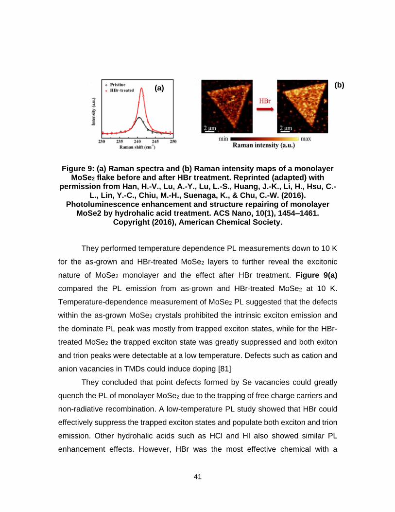
41
Figure 9: (a) Raman spectra and (b) Raman intensity maps of a monolayer MoSe2 flake before and after HBr treatment. Reprinted (adapted) with
permission from Han, H.-V., Lu, A.-Y., Lu, L.-S., Huang, J.-K., Li, H., Hsu, C.-L., Lin, Y.-C., Chiu, M.-H., Suenaga, K., & Chu, C.-W. (2016).
Photoluminescence enhancement and structure repairing of monolayer MoSe2 by hydrohalic acid treatment. ACS Nano, 10(1), 1454–1461.
Copyright (2016), American Chemical Society.
They performed temperature dependence PL measurements down to 10 K
for the as-grown and HBr-treated MoSe2 layers to further reveal the excitonic
nature of MoSe2 monolayer and the effect after HBr treatment. Figure 9(a)
compared the PL emission from as-grown and HBr-treated MoSe2 at 10 K.
Temperature-dependence measurement of MoSe2 PL suggested that the defects
within the as-grown MoSe2 crystals prohibited the intrinsic exciton emission and
the dominate PL peak was mostly from trapped exciton states, while for the HBr-
treated MoSe2 the trapped exciton state was greatly suppressed and both exiton
and trion peaks were detectable at a low temperature. Defects such as cation and
anion vacancies in TMDs could induce doping [81]
They concluded that point defects formed by Se vacancies could greatly
quench the PL of monolayer MoSe2 due to the trapping of free charge carriers and
non-radiative recombination. A low-temperature PL study showed that HBr could
effectively suppress the trapped exciton states and populate both exciton and trion
emission. Other hydrohalic acids such as HCl and HI also showed similar PL
enhancement effects. However, HBr was the most effective chemical with a
(a) (b)

42
suitable acidity and thus gave better controllability for tailoring the optical
properties of MoSe2. The drastic modulation of optical properties by HBr could be
attributed to various reasons, including removing impurities, p-doping to the MoSe2
and reducing the structure of MoSe2 [81]
Figure 10: (a) PL intensity mappings of an individual MoSe2 flake before and after HBr treatment. Profiles in (b) and (c) show the PL intensity and
photon energy modulation as a function of surface location along the solid line indicated in (a) Reprinted (adapted) with permission from Han, H.-V., Lu, A.-Y., Lu, L.-S., Huang, J.-K., Li, H., Hsu, C.-L., Lin, Y.-C., Chiu, M.-H., Suenaga, K., & Chu, C.-W. (2016). Photoluminescence enhancement and
(a)
(b) (c)

43
structure repairing of monolayer MoSe2 by hydrohalic acid treatment. ACS Nano, 10(1), 1454–1461. Copyright (2016), American Chemical Society.
Figure 11: (a) Photoluminescence of the as-grown and HBr-treated monolayer MoSe2 at 10 K. (b) Temperature dependence of PL for the MoSe2 after HBr treatment. (c) Trion and exciton peak energies. (d)
Intensity of trion to exciton peak as a function of temperature. Reprinted (adapted) with permission from Han, H.-V., Lu, A.-Y., Lu, L.-S., Huang, J.-K., Li, H., Hsu, C.-L., Lin, Y.-C., Chiu, M.-H., Suenaga, K., & Chu, C.-W. (2016). Photoluminescence enhancement and structure repairing of monolayer
MoSe2 by hydrohalic acid treatment. ACS Nano, 10(1), 1454–1461. Copyright (2016), American Chemical Society.
(a) (b)
(d) (c)

44
Guru P. Neupaneet. Al. (2017) showed that dipping 1Ls of MoS2, WS2 and
WSe2, whether exfoliated or grown by chemical vapor deposition, into methanol
for several hours can increase the electron density and could reduce the defects,
resulting in the enhancement of their photoluminescence, light absorption and the
carrier mobility[82]. This methanol treatment was effective for both n-and p-type
1L-TMDs, suggesting that the surface restructuring around structural defects by
methanol was responsible for the enhancement of optical and electrical
characteristics. Averaged PL spectra taken from the pristine state and from 16 h-
treated 1L-MoS2 indicated that an overall 2.2-fold enhancement was obtained from
this methanol treatment. Besides the increase of the PL intensity, a redshift of the
A exciton peak was also observed after the methanol treatment. PL intensity was
monotonically increased, and the peak wavelength of the A exciton peak up to 16
h were observed. The redshift of the PL peak of 1L-MoS2 has been attributed to
an increase in the trion spectral weight, indicating that the methanol treatment
caused an increase of the electron density in 1L-MoS2. Intensity ratio of trions (A−)
to neutral excitons (A0) was found to increase from 1.1 to 2.3 as the methanol
treatment time was increased from 0 to 16 h[74]
Averaged absorption spectra revealed that the increase in absorption was
specifically due to increases in the intensities of the A, B, and C exciton peaks,.
The methanol treatment seemed effective both for the exfoliated and CVD grown
samples. they suggested that the adsorption and dissociation of methanol
occurring on the surface of TMDs. Previously, a density function theory study
reported that methanol would favorably adsorb and dissociate on the edges of
MoS2 clusters through O•H dissociation and then the pathway of CH3O →CH3
→CH2. In the previous result of PL enhancement of 1L-MoS2 using organic
superacid of bis(trifluoro-methane) sulfonamide (TFSI), hydrogenation by TFSI
was regarded to be the most responsible for the fixation of the defects. Based on
such reports, they believed that consecutive hydrogen release occurring during
methanol dissociation at the defect sites of 1L-MoS2 and other TMD samples may
be responsible for the fixation of the defect states. Moreover, CH3O and CH3 are

45
known as electron-donating groups which may have induced the n-doping of our
1L-TMDs and the exfoliated MoS2 film samples(Neupane et al., 2017b).
Shinichiro Mouri et. al. (2013) demonstrated the tunability of the
photoluminescence (PL) properties of monolayer (1L)-MoS2 via chemical
doping[36]. The PL intensity of 1L-MoS2 was drastically enhanced by the
adsorption of p-type dopants with high electron affinity but reduced by the
adsorption of n-type dopants. This PL modulation resulted from switching between
exciton PL and trion PL depending on carrier density in 1L-MoS2. Extraction and
injection of carriers in 1L-MoS2 by this solution based chemical doping method
enabled convenient control of optical and electrical properties of atomically thin
MoS2. Optically generated electron−hole pairs in 1L-MoS2 form stable exciton
states even at room temperature because of the extremely large Coulomb
interactions in atomically thin two-dimensional materials. The stable exciton plays
an important role in the optical properties of 1L-MoS2. They mentioned that control
of the carrier density was one effective method to modulate the optical properties
of monolayer TMDs. The interplay between the exciton and charge carrier gave
rise to the formation of a many-body bound state such as a charged exciton (trion)
providing additional pathways for controlling the optical properties of 1L-MoS2. The
PL intensity of 1L-MoS2 was drastically enhanced when p-type dopants covered
its surface. This enhancement was understood because of switching the dominant
PL process from the recombination of the negative trion to the recombination of
the exciton under extraction of residual electrons in as-prepared 1L-MoS2. On the
other hand, the PL intensity was reduced when 1L-MoS2 was covered with n-type
dopants, which was due to the suppression of exciton PL by the injection of excess
electrons. They confirmed that bi-directional control of the Fermi level of 1L-MoS2
by chemical doping. The PL intensity of 1L-MoS2 was drastically enhanced by the
adsorption of p-type dopants (F4TCNQ and TCNQ). This intensity enhancement
was explained by the switching of the dominant PL process from the recombination
of negative trions to the recombination of excitons through extraction of the
unintentionally high doped electrons. Moreover, the PL intensity was reduced by
the adsorption of n-type dopants (NADH), which they referred to the suppression

46
of exciton PL through injection of the excess electrons. Their findings suggested
that both the extraction and the injection of electrons in 1L MoS2 could be realized
via the solution-based chemical doping technique, which provides a strong
advantage in tuning the optical and electrical properties of atomically thin TMDs
without the use of device structures. The PL intensity increases step by step with
increases in the F4TCNQ doping steps, approximately three times greater than that
of as prepared 1L-MoS2[36].
Figure 12: (a) Optical images of as-prepared 1L-, 2L-, and 3L-MoS2 on SiO2/Si substrates. (b) Raman spectra of the as-prepared 1L-, 2L-, and 3L-
MoS2 measured at room temperature. (c) PL spectra of the as prepared 1L-, 2L-, and 3L-MoS2. The PL peak due to the indirect band gap transition is denoted as I, and those due to the direct band gap transition are denoted
as peaks A and B[36](Mouri et al., 2013). Reprinted (adapted) with permission from Mouri, S., Miyauchi, Y., & Matsuda, K. (2013). Tunable

47
photoluminescence of monolayer MoS2 via chemical doping. Nano Letters, 13(12), 5944–5948. Copyright (2016) American Chemical Society
Figure 13: (a) PL spectra of 1L-MoS2 before and after F4TCNQ doping. (b) PL spectra of 1L-MoS2 obtained at each doping step (0, 1, 2, 4, 6, 10, 13, and
16 steps). The inset shows the normalized PL spectra of 1L-MoS2 at each doping step. (c) Analysis of the PL spectral shapes for as-prepared and
F4TCNQ-doped 1L-MoS2. The A peaks in the PL spectra were reproduced by assuming two peaks with Lorentzian functions, corresponding to the trion (X−) and the exciton (X) peaks, were overlapped. (d) Integrated PL intensity
of the negative trion Ix−, exciton Ix, and the sum (Itotal) of Ix and Ix−as functions of the number of F4TCNQ doping steps. Solid lines show the
calculated PL intensity curves calculated by solving the rate equations in the three-level model. Reprinted (adapted) with permission from Mouri, S.,
Miyauchi, Y., & Matsuda, K. (2013). Tunable photoluminescence of monolayer MoS2 via chemical doping. Nano Letters, 13(12), 5944–5948.
Copyright (2013) American Chemical Society.

48
Figure 14: (a) PL spectra of 1L-MoS2 before and after being doped with p-type molecules (TCNQ and F4TCNQ). (b) PL spectra of 1L-MoS2 before and after being doped with an n-type dopant (NADH). Reprinted (adapted) with
permission from Mouri, S., Miyauchi, Y., & Matsuda, K. (2013). Tunable photoluminescence of monolayer MoS2 via chemical doping. Nano Letters,
13(12), 5944–5948. Copyright (2013) American Chemical Society
Matin Amani et. al. (2016) developed a chemical treatment technique using
an organic non-oxidizing superacid, bis(trifluoro-methane) sulfonimide (TFSI),
which was shown to improve the quantum yield in MoS2 from less than 1% to over
95%[83]. They performed detailed steady-state and transient optical
characterization on some of the most heavily studied direct bandgap 2D materials,
specifically WS2, MoS2, WSe2 and MoSe2, over a large pump dynamic range to
study the recombination mechanisms present in these materials. Then they
explored the effects of TFSI treatment on the PL QY and recombination kinetics
and the results suggested that sulfur-based 2D materials were able to
repair/passivation by TFSI, while the mechanism was thus far ineffective on
selenium based systems. They also showed that biexcitonic recombination was
the dominant non-radiative pathway in these materials[83].

49
Their surface inspection revealed the following findings:
(i) high spatial variation even across the same material with the largest
imperfection density found on MoS2[83]
(ii) sulfide surfaces were dominated by structural defects and by acceptor
impurities causing local depressions[83] and
(iii) selenide surfaces were predominantly dominated by hillock-like
structures induced by donor impurities. This drastic difference in the
nature of defects may explain why sulfur-based TMD materials were
more responsive to the TFSI treatment. They showed dominant
recombination pathway at high pump-power for all these materials was
biexcitonic recombination[83].
TMDs have exhibited poor luminescence quantum yield (QY)—that is, the
number of photons the material radiates is much lower than the number of
generated electron-hole pairs. The prototypical 2D material molybdenum disulfide
(MoS2) was reported to have a maximum QY of 0.6%, which indicated a
considerable defect density[83]. QY values ranging from 0.01 to 6% have been
reported, indicating a high density of defect states and mediocre electronic quality.
The origin of the low quantum yield observed in these materials was attributed to
defect-mediated non-radiative recombination and biexcitonic recombination at
higher excitation powers surface passivation by chemical treatments. With the use
of this process, the photoluminescence (PL) in MoS2 monolayers increased by
more than two orders of magnitude, resulting in a QY > 95% and a characteristic
lifetime of 10.8±0.6 ns at low excitation densities. The treatment has eliminated
defect-mediated non-radiative recombination. Superacids are strong protonating
agents and have a Hammett acidity function (H0) that is lower than that of pure
sulfuric acid. The PL spectra of a MoS2 monolayer measured before and after TFSI
treatment in Figure 15 (b) showed a 190-fold increase in the PL peak intensity,
with no change in the overall spectral shape. The exact mechanism by which the
TFSI passivated surface defects was not fully understood in their study. Deep-level
traps—which contributed to defect-mediated non-radiative recombination,

50
resulting in a low QY—were observed for all these cases. The strong protonating
nature of the super acid could remove absorbed water, hydroxyl groups, oxygen
and other contaminants on the surface. Although these reactions would not
remove the contribution of defects to non-radiative recombination, they would open
the active defect sites to passivation by a second mechanism. One possibility was
the protonation of the three dangling bonds at each sulfur vacancy site[83].

51
Figure 15: PL spectra for both the as-exfoliated and TFSI treated (a) WS2, (b) MoS2, (c) WSe2, and (d) MoSe2 monolayers measured at an incident
power density of 1 × 10⁻² Wcm−2. The inset shows normalized spectra for each material. Absorption spectra of both as-exfoliated (dashed lines) and chemically treated (solid lines) WS2, MoS2, WSe2, and MoSe2 monolayers
(e). Reprinted (adapted) with permission from Amani, M., Taheri, P., Addou, R., Ahn, G. H., Kiriya, D., Lien, D.-H., Ager III, J. W., Wallace, R. M., & Javey,
A. (2016). Recombination kinetics and effects of superacid treatment in sulfur-and selenium-based transition metal dichalcogenides. Nano Letters,
16(4), 2786–2791. Copyright (2016) American Chemical Society.
Figure 16: Radiative decay of as-exfoliated (a) and chemically treated (b) WS2 at various initial carrier concentrations (n0) as well as the instrument response function (IRF). Reprinted (adapted) with permission from Amani, M., Taheri, P., Addou, R., Ahn, G. H., Kiriya, D., Lien, D.-H., Ager III, J. W., Wallace, R. M., & Javey, A. (2016). Recombination kinetics and effects of
superacid treatment in sulfur-and selenium-based transition metal dichalcogenides. Nano Letters, 16(4), 2786–2791. Copyright (2016)
American Chemical Society.
Matin Amani et. al. (2016) have performed a thorough exploration of
chemical treatment on CVD-grown MoS2 samples[84]. They showed that the PL
QY of CVD-grown monolayers could be improved from ∼0.1% in the as-grown
case to ∼30% after treatment, with enhancement factors ranging from 100 to
1500X depending on the initial monolayer quality. Defects act as non-radiative
recombination centers and significantly quenched the emission. Previously, it was
demonstrated that treatment using the organic superacid bis(trifluoro-methane)
sulfonamide (TFSI) resulted in a PL QY near 100% in exfoliated MoS2 monolayers
and it was later demonstrated that this treatment mechanism was also effective on

52
exfoliated WS2 monolayers. They also studied the effect of the sulfur precursor
temperature during growth and showed that this also played a role in the ultimate
quantum yield, which could be achieved after treatment. They also found that after
TFSI treatment the PL emission from MoS2films was visible by eye despite the low
absorption (5−10%)[84].
Figure 17: (a) Configuration of the growth setup utilized to prepare the MoS2 samples for this study. The temperature of the substrate and
molybdenum precursor (in the furnace hot zone) and the sulfur precursor (surrounded by heating tape) is controlled and measured independently. (b
and c) Schematic illustrating the two primary sample preparation routes investigated in this study. As-grown MoS2 triangular domains and films,
which show tensile strain after growth were either (b) treated by TFSI directly, resulting in a small reduction in the PL QY, or (c) transferred from the growth substrate using a PMMA-mediated transfer process, releasing the strain, and subsequently treated by TFSI, resulting in a final PL QY of approximately 30%. Reprinted (adapted) with permission from Amani, M., Burke, R. A., Ji, X., Zhao, P., Lien, D.-H., Taheri, P., Ahn, G. H., Kirya, D.,
Ager III, J. W., & Yablonovitch, E. (2016). High luminescence efficiency in

53
MoS2 grown by chemical vapor deposition. ACS Nano, 10(7), 6535–6541. Copyright (2016) American Chemical Society.
Figure 18: (a) Raman spectra measured on as-grown and transferred MoS2 single domains. (b) PL spectra of the MoS2 single domains measured
before and after transfer at a laser power of 50 W/cm2. Reprinted (adapted) with permission from Amani, M., Burke, R. A., Ji, X., Zhao, P., Lien, D.-H., Taheri, P., Ahn, G. H., Kirya, D., Ager III, J. W., & Yablonovitch, E. (2016).
High luminescence efficiency in MoS2 grown by chemical vapor deposition. ACS Nano, 10(7), 6535–6541. Copyright (2016) American
Chemical Society.
Figure 19: (a) Raman spectra measured on transferred MoS2 single domains before and after treatment by TFSI. (b) PL spectra obtained at a
pump power of 0.1 W/cm2 for transferred MoS2 single domains both before and after chemical treatment by TFSI. (c) Radiative decay of transferred MoS2 single domains obtained at a pump fluence of 5 × 10⁻²μJ/cm2 both before and after chemical treatment by TFSI, as well as the instrument
response function (IRF). Reprinted (adapted) with permission from Amani, M., Burke, R. A., Ji, X., Zhao, P., Lien, D.-H., Taheri, P., Ahn, G. H., Kirya, D., Ager III, J. W., & Yablonovitch, E. (2016). High luminescence efficiency in

54
MoS2 grown by chemical vapor deposition. ACS Nano, 10(7), 6535–6541. Copyright (2016) American Chemical Society.
Figure 20: (a) Optical image of a transferred MoS2 single domain and log-scale luminescence images from the same area obtained (b) before and (c)
after chemical treatment by TFSI. (d) Optical image of a transferred continuous MoS2 film and log scale luminescence images from the same
area obtained (e) before and (f) after chemical treatment by TFSI[84]. Reprinted (adapted) with permission from Amani, M., Burke, R. A., Ji, X.,
Zhao, P., Lien, D.-H., Taheri, P., Ahn, G. H., Kirya, D., Ager III, J. W., & Yablonovitch, E. (2016). High luminescence efficiency in MoS2 grown by
chemical vapor deposition. ACS Nano, 10(7), 6535–6541. Copyright (2016) American Chemical Society.
Long Yuan et. al. (2015) systematically investigated the exciton dynamics
in monolayered, bilayered and trilayered WS2 using time-resolved PL under
conditions with and without exciton–exciton annihilation.They choose WS2 as a
model system because of the relatively low defect density in WS2 as shown by the
higher photoluminescence (PL) quantum yield (QY) than other 2D semiconductors
(∼6% in WS2, compared to ∼0.1% of MoS2). Exciton decays of the monolayer,
bilayer and tri layer all exhibit mono-exponential decay behavior. The PL lifetime
was measured to be 806 ± 37 ps, 401 ± 25 ps, and 332 ± 19 ps for WS2 monolayer,
bilayer and trilayer respectively, when free of exciton annihilation. The radiative
lifetime of excitons was determined to be ∼13 ns, ∼400 ns and ∼830 ns for the
monolayer, bilayer and trilayer, respectively. Furthermore, two orders of magnitude
enhancement of the exciton–exciton annihilation rate had been observed in the

55
monolayer compared to the bilayer and trilayer. They mentioned the strongly
enhanced annihilation in monolayered WS2 to enhance electron hole interactions
and to the transition to the direct semiconductor, which eliminated the need for
phonon assistance in exciton–exciton annihilation. Another hallmark of low-
dimensional electronic systems was the enhanced many-body interaction due to a
reduced dimensionality. Upon the generation of a high density of electrons and
holes, many-body scattering processes such as Auger recombination and exciton–
exciton annihilation could play an important role in nonradiative relaxation. These
nonradiative recombination processes defined the upper limit of excitation density
and ultimately the efficiency for applications such as semiconductor lasers and
light-emitting diodes. Exciton–exciton annihilation and Auger recombination have
been intensively investigated in quantum dots, carbon nanotubes and
semiconductor nanowires. While recent studies on MoS2, MoSe2 and WSe2
monolayers have shown the existence of exciton–exciton annihilation at high
excitation density.
Yumeng You et. al. (2015) demonstrated the existence of four-body,
biexciton states in monolayer WSe2. The biexciton is identified as a sharply defined
state in photoluminescence at high exciton density. Its binding energy of 52 meV
is more than an order of magnitude greater than that found inconventional
quantum-well structures. A variational calculation of the biexciton state reveals that
the high binding energy arises not only from strong carrier confinement, but also
from reduced and non-local dielectric screening[85]
Huizhen Yao et. al. (2018) reported that CVD-grown WS2 monolayers by a
simple immersion treatment method with an available sulphur based salt. After
chemical treatment with Na2S solution, the PL emission of triangular WS2
monolayers became homogeneous and was enhanced by 25-fold in the inner
region. The PL peak wavelength after Na2S treatment had an obvious red-shift,
which was attributed to the increase of trion and biexciton formation due to an
effective n-type doping[75]
They further investigated the PL enhancement by carefully adjusting the
Na2S solution to a lower concentration level of 0.02 M. Compared with 0.05 M
56
Na2S solution treatment, partial PL enhancement and a red shifted peak
wavelength around the edge regions of WS2 monolayers. It could be attributed to
the higher chemical reactivity of the WS2 edges which may adsorb chemical
species more easily. The results indicated that the chemical interaction between
the WS2 monolayers and S2−in the solution occurs slowly from the edge towards
the inner region and the electrons are gradually injected during the chemical
treatment process[75]
The result of XPS showed that the WO3−X has been effectively reduced after
the chemical treatment. The synergistic effect of charge doping and removed
impurities made remarkable modulation of the optical properties in WS2
monolayers [75].
Zhengyu He et al. (2016) studied biexciton emission in bilayer WS2 grown
by chemical vapor deposition as a function of temperature. A biexciton binding
energy of 36±4 meV is measured in the as-grown bilayer WS2 containing 0.4%
biaxial strain as determined by Raman spectroscopy. The biexciton emission was
difficult to detect when the WS2 was transferred to another substrate to release the
stain. Density functional theory calculations show that 0.4% of tensile strain lowers
the direct band gap by about 55 meV without significant change to the indirect
band gap, which can cause an increase in the quantum yield of direct exciton
transitions and the emission from biexcitons formed by two direct gap excitons.
They found that the biexciton emission decreases dramatically with increased
temperature due to the thermal dissociation, with an activation energy of 26 ± 5
meV[86].
From extensive literature studies on PL enhancement of different TMDs, we
can specify and select which novel chemical reagents we can use for surface
passivation eventually leading to achieve the goal of this thesis. Furthermore,
above studies also showed the probable mechanism behind each treatment that
also helps understanding possible mechanism related to H2SO4-vapor treatment
that has been done in this thesis.

57
Chapter 4: Experimental Details
Chapter 4 covers the experimental part of this master’s thesis. Chapter 4
discusses about Experimental Details and Results of CVD growth of monolayer
WS2 on SiO2 (300 nm)/Si substrate, Characterization of CVD growth of monolayer
WS2 on SiO2 (300 nm)/Si substrate and focuses on Laser Power Dependence PL
measurement of pristine WS2, PL variation along certain lines for pristine WS2.
4.1. Materials
Based on Chapter 3, the experimental design and details are being
achieved and after performing multiple trial and errors, I arrived to specific
experimental details that gives good and repetitive results. For the experiment, we
have used WO3 (Sigma Aldrich, >99.5% purity) and S (Sigma Aldrich, >99.5%
purity) as precursors. The SiO2 (300 nm)/Si wafers were brought from Wafer Pro
(Diameter: 100 mm, Orientation: <100>, Single Side Polished). The substrates
were cut using diamond cutter into following dimensions:
Bottom substrate at downstream that carries WO3 powders: 4.5 cm x 3 cm
Top substrate face down for growing monolayer WS2: 4 cm x 2 cm
Substrate at the upstream end carries S powder: 4.5 cm x 4.5 cm
(a) (b)

58
Figure 21: (a) CVD Setup in the ENSC Cleanroom, (b) Image representing reaction at High Temperature in CVD Furnace
The other things we have used are small quartz tube and boat that carries
the quartz tube. The dimension of small quartz tube is given below:
Small Quartz Tube: 30 cm length, 6 cm diameter, one side open and other side
closed.
Figure 22: Schematic of Small Quartz Tube and Boat/Holder
We have used TemPress 3-zone manual heating furnace for our CVD growth. We
used OHAUS as weight balance.
4.2. Experiment
4.2.1. CVD Growth of monolayer WS2 on SiO2/Si substrate
It has been proposed that metal oxide precursors in the gas phase undergo
a two-step reaction during CVD growth, where transition metal sub-oxides are
likely formed first and then the sulfurization of these sub-oxides leads to the
formation of TMDs. The experimental procedure is divided into two sections (1)
Growth of monolayer triangular WS2 and (2) Verification of successful growth of
2D-monolayer WS2 using multiple characterization techniques such as Raman,
AFM, PL, XPS, TEM, SEM and EDS, Optical Imaging. It is worth mentioning that
we were able to grow monolayer WS2 flakes directly on Si3N4 supported-TEM grid.
The experiment is specifically designed to grow monolayer 2D materials with
different temperature zones. At first, we have used a 3-heating zone furnace

59
(TemPress) to grow monolayer triangular WS2using a bottom-up CVD process.
We have performed multiple trial and error methods (~57 trial and error) for
confirmation of getting same results each time. Before performing the CVD
process the SiO2 (300 nm) / (500 µm) Si was cleaned properly using RCA and then
Acetone, IPA and water, then blow dried using N2 gas. We have used WO3 (500
mg, >99.5% Purity, Sigma Aldrich) and S (1g, >99.5% Purity, Sigma Aldrich) as
precursors and SiO2 (300 nm)/Si substrate (WaferPro) as bottom and growth
substrate-face down approach. These precursors are positioned at different
temperature zones, which are identified with respect to their melting temperatures
~800⁰C and ~180⁰C.The bottom substrate was used to carry one of the precursors
WO3 (mg). Here, we have used Ar gas at 2 SCFH flow rate to carry the S vapor
and facilitate the reaction and formation of 2D monolayer triangular WS2 on the
growth substrate. Specific parameters such as precursor amount, growth
substrate, growth pressure and flow rate, temperature, use of gases, growth time,
use of promoter, pre-surface treatment of substrate etc. play an important role the
growth morphology, mechanism, luminescence yield, Raman spectra and light
absorption/transmission. So far, the results we achieved is average lateral crystal
size is more than ~20-25 µm and the largest crystal size is ~75 µm. For addressing
the experiment properly, a schematic experimental set-up has been shown in
Figure 23. It is important here to mention that the side from which Ar gas is flowing
at atmospheric pressure is called Up-stream and the side which is connected to
the exhaust can be called Down-stream. Therefore, the substrate which is carrying
S precursor is close to Up-stream and substrate carrying WO3 precursor and
substrate for growth facing down is close to Down-stream.

60
(a)
(b)

61
Figure 23: (a) Schematic Experimental Set-Up of CVD growth, (b) 3D view of CVD Growth of monolayer WS2 on SiO2/Si
Figure 24: Temperature profile as a function of Time for CVD growth of monolayer WS2
Figure 24 shows the Temperature profile as a function of Time for CVD
growth of monolayer WS2. As we have mentioned before our furnace is manually
operated, it was difficult for us to control the temperature of Zone 2, because Zone
3 was at very high temperature, heat was dissipated to Zone 2 by convection.
Based on the facilities we have; we are able to grow by maintaining the Zone 2
temperature at moderate level by playing with recipe.
After performing the CVD process, the growth substrate was taken out
carefully to minimize contamination by the remaining WO3 powder on the bottom
substrate and checked under optical microscope (OLYMPUS MX40). The optical
images have been shown in Figure 25. Optical images play a vital role for initial
confirmation of triangular monolayer because from optical images we can
differentiate among WS2 continuous film, multilayer (bi/tri-layer) and triangular
monolayer (different color corresponds to different thickness of the 2D material).
After confirming deposition on the growth substrate under optical microscope, the
substrates have been kept in vacuum desiccator for prevention of O2 exposure that
affects the crystal quality.

62
Table 1: CVD process parameters for monolayer WS2 growth
Distance
(Ds)
Precursor
Amount
Temperature
(Ts)
Ramp Rate
(C/min)
Holding
Time
(ts)
Press
ure
Flow
Rate
(SCFH)
Position
of
Substrate
16 cm
between
two
precursors
WO3:
500mg
S:1 gm
Zone 3:
50⁰C to 100⁰C;
100⁰C to
550⁰C;
550⁰C to
800⁰C
Zone 2: 50⁰C
to 100⁰C;
100⁰C to
180⁰C
(reaches upto
320ºC)
Zone 1: 50⁰C
to 100⁰C
Zone 3:
20⁰C/min;
20⁰C/min;
3⁰C/min
Zone 2:
20⁰C/min;
20⁰C/min
Zone 1:
20⁰C/min
30 min Atmos
pheric
2 Face-
Down
Table 1 lists the process parameters optimized for 2D monolayer WS2. For
monolayer formation, radical vapor ratio is also crucial; therefore, substrate
temperature and their spatial locations are carefully adjusted. Ds indicates the
distance between WO3 and S precursors in face-down growth configuration and
TS indicates the temperature of the substrate. In brief, when the deposition
temperature is reached, S vapor reduces WO3 powder to volatile sub-oxides
producing intermediate products such as WO2 or WO3-x [53], [87] and the formed
radicals diffuse on the substrate reacting with sulphur. Monolayer formation is
realized by the equations (1 and 2).
WO3 + S →WO3-x + S ------------------------------(3)
WO3-x + S → WS2 + SO2----------------------------(4)

63
In general, precursor ratio (in fact, the dissociated radicals’ ratio) has been
one of the essential internal parameters determining the monolayer formation. The
optimal sulfurization process can be completed by controlling this ratio carefully.
As the deposition duration is finished, a rapid cooling down process needs to be
carried out to avoid other products such as multi-layer growth of WS2 where 2
SCFH of nitrogen gas (99.999%) is purged in the tube.
The whole CVD chamber has 3-zone but for this experiment, zone 3 and
zone 2 has been used whereas zone 1 is kept empty. Zone 3 has three
temperature profiles (1) 50⁰C to 100⁰C at ramping rate of 20⁰C/min, (2) 100⁰C to
550⁰C at ramping rate of 20⁰C/min and (3) finally, 550⁰C to 800⁰C at ramping rate
of 3⁰C/min and holding time of 30 minutes. On the other hand, The temperature of
zone 2 has two temperature profiles: (1) 50⁰C to 100⁰C at ramping rate of 20⁰C/min,
(2) 100⁰C to 180⁰C at ramping rate of 20⁰C/min and holding time of 30 minutes and
as zone 1 is not participating this process and kept empty, it has only one
temperature profile: (1) 50⁰C to 100⁰C at ramping rate of 20⁰C/min. Constant flow
of Ar gas was maintained at the beginning of the process. Moreover, before
performing each run, Ar gas is purged in the reaction chamber for 5 minutes to
reduce the possibility of any contamination. Regular cleaning of quartz tube is also
important (Wang, Feng et al. 2013) and has been done with Acetone, IPA and
water. The distance between the precursors of sulphur and WO3 is kept at 16 cm.
We performed micro Raman and PL spectral characterizations with
inViaTMQontor confocal Reinshaw system and Leica TCS SP5 II- The Broadband
Confocal system at room temperature where we used 514 nm and 488 nm
excitation wavelength respectively. We obtained the images of the flakes by
confocal optical microscopy (OLYMPUS MX40). Room Temperature Laser Power
Dependent (270 µW, 193 µW, 119 µW, 58 µW, 18 µW) PL and PL variation with
distance along certain lines at 193 µW Laser Power has been performed as well
using the same PL system.

64
4.3. Experimental Results & Discussions
4.3.1. Optical
As we have mentioned before, Optical imaging is very important to
differentiate between monolayers, bi/tri-layers and multilayers based on the
contrast. Two things here play important role: (1) types of substrate such as
SiO2/Si, Quartz and Sapphire and (2) if the substrate is SiO2/Si, then thickness of
SiO2. SiO2 with ~300 nm thickness has better visibility in nanoscale. The difference
in color contrast of each number of layers is clearly visible in SiO2/Si substrate as
it matches the right thickness. The magnification we have used is 80X.
Figure 25 (a) and (b) shows the images of the monolayer WS2 flake images
obtained by con-focal optical microscopy (Olympus MX40). According to reported
studies, our samples contain smaller flakes at the center of the substrate whereas
flakes get larger when we get closer to the edge of the substrate. We can assume
that the edge of SiO2/Si substrate have more dangling bonds possibly act as more
nucleation and further horizontal growth site. As a result of the described growth
procedure, the results we achieved are average lateral crystal size is ~20-25 µm
and the largest crystal size is ~75 µm. After performing multiple trial and error
methods by slightly changing the crucial parameters, we observed that flakes
touch, overlap or merge to form larger depending on which parameters have been
changed such as holding time (ts), growth temperature (Ts), Ds, precursor ratio,
rate of sulphurization etc. Continuous WS2 film formation occurs in TMDs by the
growth of individual flakes and their coalescence or merging[88], [89] .Therefore,
with greater holding time, the flakes usually grow larger till they merge to form a
continuous monolayer film or vertical growth of flake can dominate forming
multilayer which is not actually goal of this study.
It has been reported that grain-boundary structure, which is not visible by
optical microscopy but can be visible in the dark field optical images which
suggests that the flakes are not epitaxially connected but rather overlapped. This
can be attributed to the amorphous SiO2 layer that does not support Van Der Waals

65
epitaxy as lattice matched sapphire and GaN would provide [53], [87]. Because of
amorphous nature of SiO2, the distribution of monolayer WS2 either at the center
or at the edge is random. For the growth of 2D TMDs seeds are needed and with
greater holding time (ts), the seeding process continues after the initial growth of
monolayer WS2, which results in multi-layer film formation shown in Figure 25 (c)
and (d).
Figure 25: (a) and (b) Monolayer WS2 on SiO2/Si substrate (c) and (d) Multilayer WS2 on SiO2/Si substrate
According to reported data, boundaries inside the flakes confirm existence
of structural defects (line defects). Some of our samples also show butterfly like
flakes revealing line defects inside the flake [90]. These line defects are labeled as
grain-boundaries inside the butterfly shape flake due to the nature of growth where
more than one flake seem to merge [90]. According to some other studies, the line
defects demonstrated inside the single flake are hardly found to be the grain-
boundary but more likely to be the defects related to the stress effect (X. Wang et
al., 2013). These dark regions are suggested to be the seeds. In our lab, we look
(a) (b)
(c) (d)
20 µm 20 µm
10 µm 10 µm

66
for the change in color contrast in between the flake and the bare substrate to have
an idea about the number of layers present in the sample. Figure 26 shows a
bright field and dark field image of the same region taken by same con-focal
microscope distinguishing monolayer and multilayer effectively.
Figure 26: (a) Optical Image under Bright Field where monolayer is visible and (b) Optical Image under Dark Field where monolayer is not visible
4.3.2. SEM &EDS
SEM (NovaNanoSEM, 30 keV, 7000X) and EDS study show the
morphological and elemental analysis of monolayer WS2. The SEM images and
EDS Spectra have been shown in Figure 27 and Figure 28. SEM images clearly
show uniform deposition of WS2 on SiO2/Si substrate, there is no overlapping or
merging of crystal that form grain boundaries for this sample. EDX study further
confirms the presence of W and S element after CVD deposition.
(a) (b)
10 µm 10 µm

67
Figure 27: SEM of CVD grown Pristine monolayer WS2
Figure 28: EDS of Pristine monolayer WS2 (a) before CVD deposition and (b) after CVD deposition
4.3.3. TEM
TEM (Hitachi) has been performed on pristine monolayer WS2 grown
directly on Si3N4 TEM grids (Low Stress Nitride TEM grids with windows, Nitride
Thickness 50 mm, Window size: 0.5 mm x 0.5 mm)to investigate the crystal
structure and the Selected Area Diffraction Pattern (SAED) shows Hexagonal
single crystalline structure in trigonal prismatic co-ordination ((Figure 29 (b)).
Monolayer WS2 shows a three-fold symmetry in terms of the two sets of spots in
its diffraction pattern, the bright ka spots (indicated by green arrow) and dark kb
(a) (b)

68
spots (indicated by blue arrow). The asymmetry of the W and S sublattices
separates the [1̅100] diffraction spots into two families: ka= {(1100), (1010̅), (011̅0)}
and ka=-kb. We are able to grow WS2 directly on TEM grids which have not been
performed before.
Figure 29: TEM of Pristine monolayer WS2 directly grown on TEM grids (a) TEM Image and (b) SAED Pattern
4.3.4. Raman Spectroscopy
The next approach was to perform characterization techniques that can
further give us confirmation about successful growth of monolayer WS2 on SiO2/Si
substrate. At first, Raman Spectroscopy (ReinshawinVia System 2000 micro-
Raman in backscattering geometry, Excitation wavelength: 514 nm polarised
green laser light, 50X objective lens on an optical microscope attached with the
Raman Spectroscopy) has been done as a fingerprint characterization technique
to identify monolayer WS2. The Raman Spectra of monolayer WS2 has been shown
in Figure 30 (a) and how number of layers depend on the intensity ratio has been
shown in Figure 30 (b).
1120̅
2̅110
100
110
(a) (b)
1120̅
011̅0
1̅100
2̅110
ka
kb
100
110

69
Figure 30: (a) Raman Spectra of monolayer WS2, (b) Intensity ratio vs Number of layers
Figure 30 (a) shows the Raman scattering spectra between 355 and 417
cm-1 that matches exactly with the [73]. Monolayer WS2 shows two characteristic
Raman peaks corresponding to in-plane vibration of W and S atoms (E12g) at 355
cm-1and the out-of-plane vibration of S atoms (A1g) at 417 cm-1where the change
in difference between these two peaks and intensity ratio IE12g/IA1
gare used as an
indicator for the number of layers[81]. When the layers decrease, the mode at 355
cm-1 shifts to the lower frequencies and the mode at 417 cm-1 shifts to higher
(a)
(b)

70
frequencies. According to literature, WS2 has three main Raman active phonon
modes (2LA(M), ~350 cm−1; E12g, ~355 cm−1; and A1g, ~418 cm−1)[91].
The 350 cm-1 peak is attributed to the 2LA (longitudinal acoustic) mode
merged with the E12g modes. The LA phonon vibrational mode, as a function of
crystalline disorder, arises from in-plane collective movements of atoms in the
lattice, while the E12g is optical mode and originates from the in-plane vibration of
S and W atoms. On the other hand, the 417 cm-1 Raman peak is the out-of-plane
vibration A1g characteristic of WS2. It has been reported that not only the frequency
difference (∆) of E12g and A1g peaks, but also the peak intensity ratio of 2LA to A1g
of WS2 is highly sensitive to its thickness. For single-layer WS2 grown on SiO2 at
an excitation wavelength of 514 nm, the height of the 2LA (E12g) peak is roughly 2
times that of the A1g peak (I2LA(E12g)/IA1g ~ 0.9 for bilayer and smaller than 0.9 for
three or more layers). Our-grown WS2 shows I2LA(E12g)/IA1g ~ 2 with a frequency
difference ~ 62 cm-1 under 514 nm excitation, which evidences that our CVD-grown
material is monolayer WS2.
4.3.5. AFM
AFM is being considered as one of the important characterization
techniques for 2D materials for measuring thickness. AFM (Bruker) has been
performed in 4D Labs to measure the thickness of monolayer WS2. The thickness
of monolayer WS2 is ~1 nm indicating successful growth of monolayer WS2; on the
other hand; the thickness of bi/tri-layer is more than 1 nm (Figure 31).
(a)

71
Figure 31: (a) AFM mapping of monolayer WS2 (b) Height profile along Blue Line,
4.3.6. XPS
X-ray Photoelectron Spectroscopy (XPS) was performed to reveal the
change of the elemental composition. The binding energy peak position of a
specific element depends on the oxidation state. The standard C 1s peak (285 eV)
is used as a reference for correcting the shifts. Figure 32 (a) shows the high
resolution XPS spectra of S 2p doublet in the pristine WS2 monolayers confirming
successful deposition of WS2 by CVD. The binding energies of S 2p3/2 and S 2p1/2
located at around 162.4 and 163.7 eV, corresponding to S2−and S22−species [75],
[83], [84], [92]–[94]((Figure 32 (a)). Three characteristic XPS peaks of WS2 at
binding energies 32.6 eV, 34.7 eV, and 37.9 eV corresponding to W4f7/2, W4f5/2,
and W5p3/2 core energy levels, respectively, are observed for tungsten (W) atom.
The W4f7/2, which represents the 4+ valence state, showing a dominant
contribution and it indicates the WO3 (6+) precursor is sufficiently sulfurized even
without employing H2 in our experimental setup. The binding energies at around
32.6 and 34.7 eV reveal the +IV chemical states of W corresponding to WS2
monolayers as shown in Figure 32 (b). As for WS2 monolayers, tungsten with a
valence electronic configuration of 6s25d4 possesses an electropositive property
and acts as an electron acceptor [75]. When electronegative S2−(electron donor)
ions in the sulphur based acid, chemical solution or vapor are incorporated into
(b)

72
WS2 monolayers, they occupy the location of sulfur vacancies or absorbed by
WO3−x species and electrons can effectively be injected into the WS2 monolayers.
In addition, the absorption of the sulphur element can effectively passivate the
structural defects and decrease the non-radiative recombination centres [75], [83],
[84]. Binding energy with respect to the doping element cannot be detected which
indicates that no extra impurity is induced after the chemical treatment. These
results further clarify that S2−in the chemical solution plays a key role in strong PL
enhancement and the chemical interaction is subsistent between the solution and
the pristine WS2.In the case of modifying a sample by adding other elements, if the
electro negativity of the doping element is higher than the base element, the
electron density around the base element decreases and the binding energy
increases. Therefore, binding energy peak shifts positively. Conversely, if the
electro negativity of the doping element is lower than the base element, the
electron density around it increases and the binding energy decreases, leading a
red shift in BE peak position. The main cause of the peak shift in XPS spectra is
mostly related to chemical shifts due to the presence or absence of the chemical
states of the element having different formal oxidation state[75], [83], [84]. The
intensity may also be changed because it is directly linked to the number of atoms
in the respective chemical state. It has been reported [75], [83], [84] that peaks at
36.1 eV and 38.2 eV are referred to as +VI chemical state compounds, such as
WO3.The presence of such peaks depends on the preparation of the sample. In
our experiment, these peaks are absent in the XPS data, assuming that our
samples are prepared in a clean way confirming no presence of WO3 residue.
Sulphur based acid, chemical solution or vapor can be used to enhance PL
because of the presence of S2−and S22−species in pristine WS2 monolayers and
the chemical interaction is subsistent between the Sulphur based acid, chemical
solution or vapor and the pristine WS2 monolayers. It has been reported that the
chemical interaction between the WS2 monolayers and sulphur based acid,
chemical solution or vapor occurs slowly from the edge towards the inner region
and the electrons are gradually injected during the chemical treatment process
eventually leading to enhanced PL[75], [83], [84], [92]–[94].

73
Figure 32: XPS Spectra of monolayer WS2 (a) S 2p, (b) Core level W 4f
4.3.7. PL
4.3.7.1. Room Temperature PL of Pristine WS2
Photoluminescence spectroscopy (Leica TCS SP5 II- The Broadband
Confocal system, 488 nm excitation wavelength, Ar laser, 193 µW laser power, 5
mints, 20X magnification with Green Filter) revealed a sharp but weak emission
peak at ~626 nm confirming indirect (bulk) to direct band-gap (monolayer)
transition in the monolayer triangular WS2as shown in Figure 33 (f).
(a)
(b)

74
(a)
(c)
(b)

75
(d)
(e)
(f)

76
Figure 33: (a,b) Fluorescence Images of monolayer WS2, (c) PL intensity map of pristine monolayer WS2, (d) 2D surface plot of Pristine WS2, (e) 3D Surface Plot of Pristine WS2and (f) PL spectra of grown monolayer WS2
Figure 33 shows the photoluminescence properties of the grown WS2
monolayers are scanned with a 488 nm laser with 5 mints integration time. Figure
33 (c) demonstrates the total PL intensity map. Figure 33 (f) shows the PL spectra
with the exciton peak at ~626 nm, this result shows excitonic emission is more
profound at the interior regions of the flake whereas luminescence is due to trion
emission at the edges. In Figure 33 (c), maximum PL intensity map contains dark
regions where we do not observe PL. As we can see from photoluminescence
image, it shows non-uniform photoluminescence and darkening at the center of
monolayer triangular WS2. To understand such results based on ongoing research
and previous studies, point defects (S vacancies) in monolayer WS2can
significantly trap free charge carriers and localize excitons, leading to the
suppressing of free band-to-band exciton emission. In general, CVD-grown TMDs
could exhibit a unique PL property which is absent in their exfoliated TMDs
counterparts. Defects within the monolayer WS2 crystal act as non-radiative
recombination sites and thus quench the intrinsic PL. The darkening of PL in the
center of WS2 islands is attributed to the presence of structural defects such as
point defects and dislocations within the metastable nuclei and charge defect
induced doping. During the CVD growth procedure, the initial nucleation occurs at
the beginning of the growth process followed by the incoming WS2species
coalescing into the nuclei leading to an enlarged grain. Point defects formed by S
vacancies can greatly quench the PL of monolayer due to the trapping of free
charge carriers and non-radiative recombination. Non-uniform PL features are
caused by structural imperfection and n-doping induced by charged defects.
Uniform PL is found to be intrinsic, intense and non-blinking, which are attributed
to high crystalline quality. Variation in PL could be responsible, including external
electrostatic doping induced by the dielectric environment, strain, absorbates/
clusters and structural defects. Defects will give rise to gap states and will reduce
the device performance. For example, sulfur vacancies are seen to reduce the

77
photoluminescence efficiencies by typically 104.Crystals having more defects in
them, such as stacking faults, twins etc., which can act as non-radiative
recombination centers. Semiconductors are characterized by two types of mobile
carriers, electrons in the conduction band and holes in the valence band. Both
bands are separated by an energy gap. When an electron loses energy and falls
into the valance band, it gets neutralized by a hole which absorbs its energy. This
process is called recombination and the energy of recombination will emerge as a
photon. Most common cause for non-radiative recombination events are defects
in the crystal structure. This effect includes unwanted foreign atoms, native
defects, dislocations. All such defects have energy level structure that are different
from substantial semiconductor atoms. And it’s quite common for such defects to
form one or several energy levels within the forbidden gap of the semiconductor.
Energy levels within the gap of the semiconductors are efficient recombination
centers. Trap assisted recombination occurs when an electron falls into a “trap”,
this is an energy level within the bandgap caused by the presence of a foreign
atom or a structural defect. Once the trap is filled it cannot accept another electron.
The electron occupying the trap, in a second step, falls into an empty valence band
state, thereby completing the recombination process. Atoms at the surface cannot
have the same bonding structure as bulks atoms due to the lack of neighboring
atoms. Thus, some of the valence orbitals do not form a chemical bond. These
partially filled electron orbitals, or dangling bonds, are electronic states that can be
in the forbidden gap of the semiconductor where they act as recombination center
leading to a reduced luminescence efficiency. Understanding of indirect to direct
band gap transition is important because high-intensity PL has appealed special
attention to study optical properties of such large-area monolayers that can be
used for novel photonic devices[87].
4.3.7.2. Room Temperature Laser Power Dependent PL of Pristine WS2
As we know, when laser light is irradiated on to the sample, light is
absorbed, and the excess energy is used in photoexcitation within the specimen.
The photoexcitation causes the electrons to promote into available excited states.

78
The electrons in these excited states would then eventually relax into a lower
equilibrium state and the excess energy is released which may result in the
emission of light (radiative process) or a nonradiative process. Thus, the energy of
the emitted light released during the relaxation of the excited electron is the
difference between the energy level of the excited state and the equilibrium state.
Therefore, with increase in laser power, the photon emission would be much higher
eventually resulting in increase of exciton peak in pristine WS2.
(a)
(b)

79
Figure 34: (a) Laser Power Dependent PL study of Pristine WS2 in terms of Wavelength (nm) and (b) Laser Power Dependent PL study of Pristine WS2
in terms of Photon Energy (eV)
From Figure 34, we can see that with the decrease of laser power, the
exciton peak tends to decrease as well corresponding to lower photon emission
and weaker PL intensity. On the other hand, with the increase of laser power, the
exciton peak tends to increase as well corresponding to higher photon emission
and higher PL intensity compared to lower laser power. The system has limitation
of using it at higher laser power, so we were only able to use 50% Ar laser power
that is equal to 272 µW. We have used power meter to accurately measure power.
Figure 35: PL Intensity variation with Laser Power in log scale
Figure 35 shows how PL intensity varies with laser power in log scale. It
shows that the relation of PL intensity of pristine WS2with laser power is almost
linear where R2 value is 0.99548. It is important to interpret this data confirming
linear relationship of PL intensity with Laser Power.

80
4.3.7.3. Room Temperature PL Variation of Pristine WS2 along certain lines
From PL intensity map we see that the pristine WS2 shows non-uniform
nature whereas the edge shows strong PL emission (brighter) corresponding to
biexciton emission according to literature and when we move from edge to middle
it starts to show weak emission specially in the middle assuming presence of more
defects or thicker region considered as seed in the middle. Therefore, it is
important to show how PL varies along lines with distance for pristine WS2. Further
study is necessary for clearly explaining the data based on STM and HRTEM study
that could potentially show presence of defects in pristine WS2.
Line 1
(a) (b)
Line 2
(c) (d)

81
(h) (g)
Line 4
Point A
Point A
Line 3
(e) (f)

82
Figure 36: PL Intensity variation along line with distance (a) PL Image of Pristine WS2 with Line 1, (b) PL variation along Line 1, (c) PL Image of Pristine WS2 with Line 2, (d) PL variation along Line 2, (e) PL Image of Pristine WS2 with Line 3, (f) PL variation along Line 3, (g) PL Image of Pristine WS2 with Line 4, (h) PL variation along Line 4, (i) PL Image of
Pristine WS2 with Line 5, (j) PL variation along Line 5 and (k) PL Image of Pristine WS2 with Line 6, (l) PL variation along Line 6
Figure 36 shows how PL intensity changes along a line within a particular flake.
Figure 36 (a), (b) and (c) shows almost uniform and higher PL intensity along Line
1, Line 2 and Line 3 whereas, along Line 5, we can see a dip in the PL intensity
corresponding to middle region of the flake probably due to presence of defect or
thicker region acting as seed for formation of pristine WS2. Higher and almost
(j) (i)
(l) (k)
Line 6
Line 5
Point B
Point B
Point C
Point C

83
uniform PL intensity along Line 1, Line 2 and Line is due to biexciton formation,
with increasing laser power (272 µW) the formation of biexciton increases resulting
in higher photoemission corresponding to stronger PL signal.

84
Chapter 5: PL Enhancement of Monolayer WS2
Chapter 5 discusses the purpose of PL enhancement, experiment, results and
discussion.
5.1. Purpose of PL Enhancement
The purpose of PL enhancement is as follows:
1. According to literature, mechanically exfoliated and CVD grown monolayer
2D materials tend to show weak PL; which is not applicable for
optoelectronics such as LED. So, what’s the solution? Surface modification
is supposed to passivate the point defects and surface vacancy/Sulphur
vacancy which ultimately reduces the non-radiative recombination sites and
show enhanced exciton peak.
2. Suppression of Phonons takes place significantly at Low Temperature (LT)
and hence enhanced PL is observed at 77K or below for 2D materials, but
we performed experiment at Room Temperature (RT); carriers at RT can
have enough energy to get to non-radiative recombination centers, so, in
general, a strong reduction of the intensity of the PL signal is observed
which is not seen in our samples at RT; according to literature excitonic
effects are more efficient at LT but for our samples exciton peak is sharp at
RT. Most of the LEDs operating temperature is ~298k not 77k; therefore, it
is important to focus on achieving enhanced PL at RT.
According to literature that has been discussed in Chapter 3, different chemical
reagents have been used to treat pristine TMDs to achieved high QY with
enhanced light emission. Still, there is scope for exploration in this field and in this
chapter H2SO4-vapor has been used for the first time for surface passivation of
pristine-WS2. The methodology is discussed below.
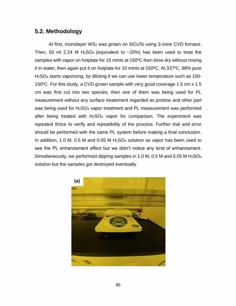
85
5.2. Methodology
At first, monolayer WS2 was grown on SiO2/Si using 3-zone CVD furnace.
Then, 50 ml 2.24 M H2SO4 (equivalent to ~20%) has been used to treat the
samples with vapor on hotplate for 15 mints at 150ºC then blow dry without rinsing
it in water; then again put it on hotplate for 10 mints at 150ºC. At 337ºC, 98% pure
H2SO4 starts vaporizing, by diluting it we can use lower temperature such as 100-
150ºC. For this study, a CVD grown sample with very good coverage 1.5 cm x 1.5
cm was first cut into two species, then one of them was being used for PL
measurement without any surface treatement regarded as pristine and other part
was being used for H2SO4 vapor treatment and PL measurement was performed
after being treated with H2SO4 vapor for comparison. The experiment was
repeated thrice to verify and repeatibility of the process. Further trial and error
should be performed with the same PL system before making a final conclusion.
In addition, 1.0 M, 0.5 M and 0.05 M H2SO4 solution as vapor has been used to
see the PL enhancement effect but we didn’t notice any kind of enhancement.
Simultaneously, we performed dipping samples in 1.0 M, 0.5 M and 0.05 M H2SO4
solution but the samples got destroyed eventually.
(a)

86
Figure 37: (a) Setup of H2SO4 Vapor Treatment in Yellow Room, (b) Schematic Setup of H2SO4-Vapor Treatment
5.3. Results and Discussion
5.3.1. PL Enhancement of H2SO4-Vapor Treated Monolayer WS2
We have already discussed the purpose of PL enhancement before. Now
let’s see the possible mechanism of PL enhancement using strong protonated
acid. Here, we will try to discuss possible mechanism of PL enhancement using
an acid based on the reported studies. To further clarify we will need to perform
High Resolution Transmission Electron Microscopy (HRTEM), Scanning Tunneling
Microscopy (STM) that will give us more details in atomic level how acid treatment
modify the structure. Performing HRTEM, STM has not been done yet because it
is beyond the scope of the master’s thesis. It is important to mention of choosing
H2SO4 among all other acids. Firstly, it is important to select an acid which can
easily donate H+ in an aqueous solution. The criteria for choosing an acid are
Hammett Acidity Function (H0). The acid ionization constants typically used to
measure weak acids' acidity are only valid in dilute aqueous solutions. A more
general measure of acidity that in principle is valid for any acid is the H0. The
Hammett acidity function, H0 is analogous to the pH used to describe the acidity of
aqueous solutions but instead refers to the pure acid:
(b)

87
pH=−log(AH+) (for dilute aqueous solutions)
H0=−log(AH+) (for pure acids)
Where, AH+ is the activity of H+ , which in many dilute solutions is approximately
equal to the hydrogen ion concentration (that is why the pH is often defined in
terms of [H+].
At first glance it may seem that the Hammett acidity function is simply a
generalization of the pH concept for use in non-aqueous solutions. This is
especially so since in water the pH and H0 do refer to the same quantity. However,
the hydrogen ion of the Hammett acidity function is more than a generalization of
the pH concept. Its real genius lies in that AH+ does not necessarily represent an
actual chemical species of identity H+ but rather an acid's ability to protonate weak
indicator bases, B, specifically via the reaction:
H++B⇌BH+--------------------------------(5)
This reaction gives the weak acid BH+ which can ionize in the reaction that is the
reverse of that above:
BH+⇌B+H+---------------------------------(6)
The extent of this ionization will depend on AH+ according to
Kion=[BH+]/AH+[B]--------------------------(7)
Taking the negative logarithm of both sides and rearranging gives the Henderson-
Hasselbach equation for the indicator base, B:
−Kion=−logAH+−log[BH+]/[B]--------------(8)
which can be rearranged to give:
pKion= H0−log[BH+]/[B]--------------------(9)
or,
H0= pKion−log[BH+]/[B]--------------------(10)
From this it is apparent that Ho represents an acid's ability to donate a hydrogen
ion, as measured in terms of its ability to shift the equilibrium between B and BH+
towards BH+. More negative values of H0 correspond to stronger Brønsted acids
with a greater hydrogen ion transfer ability while less negative ones indicate
weaker Brønsted acidity. The value of H0 has been experimentally determined for
a number of strong acids by measuring the ratio of BH+ to B using weakly basic

88
aromatics like 2,4,6-trinitroaniline, various nitrotoluenes and trifluoromethyl-
benzene as the indicator base, B. Sulfuric Acid has a Hammett acidity of -11.3.
Since superacids are defined as acids with greater Brønsted acidity than pure
sulfuric acid this means that superacids have (H0<11.3]. A list of organic and
inorganic acid is given below based on H0 that can be used further for future studies
of PL enhancement:
1. Fluoroantimonic acid (H0 = −21 and −23 respectively)
2. Hydrogen fluoride (H0 = −15.1)
3. TFSI (H0 = −14) with 1,2-Dichloroethane (as solvent)
4. HClO4 (H0= -12)
5. Sulfuric Acid (H0 = −11.3)
From the above list, TFSI has already been used widely for PL
enhancement of TMDs. The function of strong acid is to supply a strongly acidic
ambient to push the equilibrium toward greater binding of hydrogen with the Mo/W
dangling bonds to passivate defect states in TMDs, the passivation method should
deactivate only the defect states without a permanent change in the intrinsic crystal
and electronic structure of TMDs. Moreover, the adsorbed molecules should be
chemically and thermally stable on TMDs; consequently, they should not
decompose or desorb during the fabrication processes or during operation under
ambient conditions.
(a) (b)

89
Figure 38: PL Intensity mapping of Pristine-WS2 (a) before and (b) after H2SO4-vapor Treatment
(a)

90
Figure 39: PL Intensity vs Wavelength (nm) before and after H2SO4-vapor treatment
Figure 40: Normalized PL Intensity vs Wavelength (nm) before and after H2SO4-vapor treatment
The PL measurement was performed using the same PL system with same
configuaration before and after surface treatment with H2SO4 vapor. The
experiment was repeated thrice but further trial and error should be performed
keeping all paramenters and configuaration constant. In chapter 4, we saw that
pristine WS2 showed PL peak at ~626 nm whereas after H2SO4 vapor treatment,
the peak shifts to ~634 nm. Figure 38 shows PL mapping of monolayer WS2 before
and after H2SO4 vapor treatment. From Figure 38, it is evident that H2SO4 vapor
has potential to passivate the surface defects of pristine WS2 that eventually
results in PL enhancement. Moreover, in Figure38 (a) the pristine WS2 shows
more PL emission from edge compared to other region, due to the formation of
biexciton. Figure 39 and Figure 40 shows PL enahncement before and after
H2SO4 Vapor treatment indicating maximum ~10 fold enhancement and on
average ~5 fold enhancement. Surface passivation by chemical treatments induce
defect-mediated non-radiative recombination and biexciton recombination. Deep-

91
level traps contributes to defect-mediated non-radiative recombination, resulting in
a low PL being observed in pristine WS2((Figure 38 (a)). The strong protonating
nature of the strong acid could remove absorbed water, hydroxyl groups, oxygen
and other contaminants on the surface of a sample. Although these reactions
would not remove the contribution of defects to non-radiative recombination, they
would open the active defect sites to passivation by a second mechanism. One
possibility of enhancement could be the protonation of the three dangling bonds at
each sulfur vacancy site.The primary focus should be on the enhancement of
exciton peak; which is being achieved in this investigation. After normalizing the
data, according to literature, acid treatment can promote sharp exciton as well as
trion emission (shifting towards right in terms of wavelength) from defective
monolayers which is relatable to the data. After H2SO4 Vapor Treatment, the PL
spectra is moving towards red-shift (in terms of wavelength) corresponding to
increase of trion emission and biexciton formation due to effective n-type doping
by vapor treatment. Based on literature search, it is possible to say with brief
explanation that the reason behind PL enhancement is because of exciton (major
peak), increase of trion emission and biexciton formation (the slight shift in peak
indicates trion emission).If the exciton encounters a defect, it may be trapped,
retaining some of its exciton character. Bound excitonic states are unstable and
will decay into stable states with less energy by emitting a photon.
5.3.2. Room Temperature Laser Power Dependent PL of H2SO4-Vapor Treated monolayer WS2
Room Temperature Laser Power Dependent (272 µW, 193 µW, 119 µW,
58 µW, 18 µW) PL study of H2SO4- vapor Treated monolayer WS2 has been
performed with the same PL system. Figure 41 shows stronger PL signal after
H2SO4- vapor treatment with increasing laser power. The reason we can predict
could be two folds: (1) surface passivation of the Sulphur vacancies due to vapor
treatment and (2) increase in laser power promotes more excitation which
eventually leads to more photoemission.

92
(a)
(b)

93
Figure 41: (a) Laser Power Dependent PL study of H2SO4-Vapor Treated Monolayer WS2 in terms of Wavelength (nm) and (b) Laser Power
Dependent PL study of H2SO4-Vapor Treated Monolayer WS2 in terms of Photon Energy (eV)
Figure 42: PL Intensity variation with Laser Power in log scale
Figure 42 shows how PL intensity varies with laser power in log scale. It
shows that the relation of PL intensity of H2SO4-vapor treated monolayer WS2 with
laser power is almost linear where R2 value is 0.93011.
5.5.3. Room Temperature PL Variation of H2SO4-Vapor Treated WS2 along
certain lines
We follow the same procedure that we showed in chapter 4, here we instead
tried to study the PL Variation of H2SO4-Vapor Treated WS2 along certain lines.

94
(f) (e)
Line 2
Line 1
Line 3
(a) (b)
(c) (d)

95
(h) (g)
(j) (i)
(l) (k)
Point A
Line 6
Point A
Line 5
Line 4

96
Figure 43: PL Intensity variation along certain line (a) PL Image of H2SO4-Vapor Treated Monolayer WS2 with Line 1, (b) PL variation along Line 1, (c)
PL Image of H2SO4-Vapor Treated Monolayer WS2 with Line 2, (d) PL variation along Line 2, (e) PL Image of H2SO4-Vapor Treated Monolayer WS2
with Line 3, (f) PL variation along Line 3, (g) PL Image of H2SO4-Vapor Treated Monolayer WS2 with Line 4, (h) PL variation along Line 4, (i) PL
Image of H2SO4-Vapor Treated Monolayer WS2 with Line 5, (j) PL variation along Line 5 and (k) PL Image of H2SO4-Vapor Treated Monolayer WS2 with
Line 6, (l) PL variation along Line 6
Figure 43 shows how PL intensity changes along a line within a particular flake
after H2SO4 vapor treatment. Figure 43 shows nearly uniform and comparatively
higher PL intensity along Line 1, Line 2 and Line 3 whereas in Figure 43 (a), (b)
and (c), along Line 6 in Figure 43 (f), we can see a dip like we saw in Chapter 4
for pristine WS2 but the PL signal is much more stronger. This study somehow
reveals that after H2SO4 vapor treatment of monolayer WS2; the PL intensity
enhances indicating nearly uniform surface passivation of Sulphur vacancies of
monolayer WS2.
5.3.4. XPS Study of H2SO4- Vapor Treated Monolayer WS2
XPS study has been done using same system in 4D labs with same
configuration that has been used for pristine WS2 in Chapter 4. Figure 108 shows
XPS spectra S 2p and core level W 4f before and after H2SO4 vapor treatment.
The slight shift in both XPS spectra indicates the surface modification has been
done by changing chemical composition. In Chapter 4, before vapor treatment, the
binding energies of S 2p3/2 and S 2p1/2 locate at around 162.4 and 163.7 eV,
corresponding to S2−and S22−species[75], [83], [84], [92]–[94] ((Figure 44 (a)).
Three characteristic XPS peaks of WS2 at binding energies 32.6 eV, 34.7 eV and
37.9 eV corresponding to W4f7/2, W4f5/2, and W5p3/2 core energy levels,
respectively in Figure 44 (b). After vapor treatment the binding energies of S 2p3/2
and S 2p1/2 locate at around 163.1 eV and 164.3 and three characteristic XPS
peaks of WS2 at binding energies 33.7 eV, 35.4 eV and 38.6 eV corresponding to
W4f7/2, W4f5/2 and W5p3/2 core energy levels, respectively[75], [83], [84], [92]–[94].
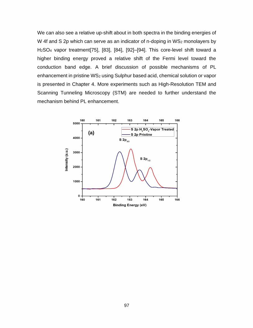
97
We can also see a relative up-shift about in both spectra in the binding energies of
W 4f and S 2p which can serve as an indicator of n-doping in WS2 monolayers by
H2SO4 vapor treatment[75], [83], [84], [92]–[94]. This core-level shift toward a
higher binding energy proved a relative shift of the Fermi level toward the
conduction band edge. A brief discussion of possible mechanisms of PL
enhancement in pristine WS2 using Sulphur based acid, chemical solution or vapor
is presented in Chapter 4. More experiments such as High-Resolution TEM and
Scanning Tunneling Microscopy (STM) are needed to further understand the
mechanism behind PL enhancement.
(a)

98
Figure 44: XPS Spectra of monolayer WS2 before and after H2SO4 vapor treatment (a) S 2p and (b) Core Level W 4f
(b)

99
Chapter 6: Future Projects & Conclusion
Chapter 6 discusses limitation, future work and conclusion.
6.1. Limitation
Further experiments should be performed with the same PL system keeping other
conditions same along with STM and HRTEM studies to verify the process. More
controllable furnace such as tube furnace is needed for controlling and introducing
Sulphur vapor more precisely.
6.2. Contribution
The main contribution of this thesis in the field of PL study, is to try surface
passivation with unique and novel chemical reagents H2SO4-vapor at room
temperature. When treated with H2SO4-vapor, pristine-WS2 shows maximum 10-
fold enhancement with enhanced exciton and trion emission at RT that has not
been studied before.
6.3. Future Work
The goal of this master’s thesis was to develop a CVD process where we can get
repeatable results, then further characterize it with different techniques and finally,
perform surface passivation using H2SO4-vapor. The goal has been achieved
successfully. Moreover, the results I have achieved can pave way for other future
projects as follows:
1. Monolayer WS2 can be used as piezo-sensors for harmful chemical and gas
detection
2. Monolayer WS2 functionalized with cytokines can be used as biosensor for
cancer detection
3. Surface passivated monolayer WS2 has potential applications in LED

100
6.4. Conclusion
In conclusion, our first approach was to get monolayer WS2 on SiO2/Si substrate
by performing CVD. We played with multiple factors to master the technique and
to get repeatable results. Then, we performed multiple characterization techniques
such as micro Raman and PL, AFM, TEM, SEM and EDX, XPS optical imaging for
confirming successful growth of monolayer WS2. The results we achieved where
the largest lateral crystal size is ~75 um and avg. lateral crystal size is more than
~20-25 um. Data regarding Raman and PL matched with the reported ones.
Photoluminescence from our pristine sample is relatively weak and the possible
reasons behind weak PL have been discussed based on previous and ongoing
studies. Then, to enhance PL we have used 50 ml 2.24 M H2SO4 vapor treatment,
showing maximum ~10 times PL enhancement and on average ~5 times PL
enhancement showing peak at ~634 nm corresponding to red-shift trion emission
compared to peak at ~626 nm for pristine-WS2. Finally, the results of some other
projects have been discussed in short that open doors for future projects with
potential applications.
Bibliography
[1] P. R. Wallace, “The band theory of graphite,” Phys. Rev., vol. 71, no. 9, p. 622, 1947.
[2] M. Sharma, L. Johnson, and J. McClure, “Diamagnetism of graphite,” Phys. Rev. B, vol. 9, no. 6, p. 2467, 1974.
[3] G. W. Semenoff, “Condensed-matter simulation of a three-dimensional anomaly,” Phys. Rev. Lett., vol. 53, no. 26, p. 2449, 1984.
[4] E. Fradkin, “Critical behavior of disordered degenerate semiconductors. II. Spectrum and transport properties in mean-field theory,” Phys. Rev. B, vol. 33, no. 5, p. 3263, 1986.
[5] F. D. M. Haldane, “Model for a quantum Hall effect without Landau levels: Condensed-matter realization of the" parity anomaly",” Phys. Rev. Lett., vol. 61, no. 18, p. 2015, 1988.
[6] J. Slonczewski and P. Weiss, “Band structure of graphite,” Phys. Rev., vol. 109, no. 2, p. 272, 1958.
[7] R. Peierls, “Quelques propriétés typiques des corps solides,” 1935, vol. 5, pp. 177–222.
[8] K. S. Novoselov et al., “Electric field effect in atomically thin carbon films,” science, vol. 306, no. 5696, pp. 666–669, 2004.

101
[9] K. S. Novoselov et al., “Two-dimensional gas of massless Dirac fermions in graphene,” nature, vol. 438, no. 7065, pp. 197–200, 2005.
[10] Y. Zhang, Y.-W. Tan, H. L. Stormer, and P. Kim, “Experimental observation of the quantum Hall effect and Berry’s phase in graphene,” nature, vol. 438, no. 7065, pp. 201–204, 2005.
[11] A. K. Geim, “Graphene: status and prospects,” science, vol. 324, no. 5934, pp. 1530–1534, 2009.
[12] A. C. Neto, F. Guinea, N. M. Peres, K. S. Novoselov, and A. K. Geim, “The electronic properties of graphene,” Rev. Mod. Phys., vol. 81, no. 1, p. 109, 2009.
[13] K. S. Novoselov, V. Fal, L. Colombo, P. Gellert, M. Schwab, and K. Kim, “A roadmap for graphene,” nature, vol. 490, no. 7419, pp. 192–200, 2012.
[14] H. Chen, “Manipulation of light-emitting properties of 2D materials by photonic nanostructures,” 2017.
[15] M. Fox, “Optical properties of solids,” 2002. [16] J. A. Wilson and A. Yoffe, “The transition metal dichalcogenides discussion and
interpretation of the observed optical, electrical and structural properties,” Adv. Phys., vol. 18, no. 73, pp. 193–335, 1969.
[17] M. Chhowalla, H. S. Shin, G. Eda, L.-J. Li, K. P. Loh, and H. Zhang, “The chemistry of two-dimensional layered transition metal dichalcogenide nanosheets,” Nat. Chem., vol. 5, no. 4, p. 263, 2013.
[18] A. Kuc, N. Zibouche, and T. Heine, “Influence of quantum confinement on the electronic structure of the transition metal sulfide T S 2,” Phys. Rev. B, vol. 83, no. 24, p. 245213, 2011.
[19] H. R. Gutiérrez et al., “Extraordinary room-temperature photoluminescence in triangular WS2 monolayers,” Nano Lett., vol. 13, no. 8, pp. 3447–3454, 2013.
[20] A. Splendiani et al., “Emerging photoluminescence in monolayer MoS2,” Nano Lett., vol. 10, no. 4, pp. 1271–1275, 2010.
[21] F. Hao, D. Fang, and Z. Xu, “Mechanical and thermal transport properties of graphene with defects,” Appl. Phys. Lett., vol. 99, no. 4, p. 041901, 2011.
[22] H. Zeng and X. Cui, “An optical spectroscopic study on two-dimensional group-VI transition metal dichalcogenides,” Chem. Soc. Rev., vol. 44, no. 9, pp. 2629–2642, 2015.
[23] C. Ballif, M. Regula, and F. Levy, “Optical and electrical properties of semiconducting WS2 thin films: From macroscopic to local probe measurements,” Sol. Energy Mater. Sol. Cells, vol. 57, no. 2, pp. 189–207, 1999.
[24] S. Z. Butler et al., “Progress, challenges, and opportunities in two-dimensional materials beyond graphene,” ACS Nano, vol. 7, no. 4, pp. 2898–2926, 2013.
[25] X. Duan, C. Wang, A. Pan, R. Yu, and X. Duan, “Two-dimensional transition metal dichalcogenides as atomically thin semiconductors: opportunities and challenges,” Chem. Soc. Rev., vol. 44, no. 24, pp. 8859–8876, 2015.
[26] D. Ovchinnikov, A. Allain, Y.-S. Huang, D. Dumcenco, and A. Kis, “Electrical transport properties of single-layer WS2,” ACS Nano, vol. 8, no. 8, pp. 8174–8181, 2014.
[27] H. R. Gutiérrez et al., “Extraordinary room-temperature photoluminescence in triangular WS2 monolayers,” Nano Lett., vol. 13, no. 8, pp. 3447–3454, 2013.
[28] B. Adilbekova, “The mechanical characterization of two-dimensional materials (WS2, MoS2, and graphene) and the effect of defects on youngs modulus of CVD grown single-layer graphene,” 2017.
[29] V. Singh, D. Joung, L. Zhai, S. Das, S. I. Khondaker, and S. Seal, “Graphene based materials: past, present and future,” Prog. Mater. Sci., vol. 56, no. 8, pp. 1178–1271, 2011.

102
[30] C. Muratore et al., “Cross-plane thermal properties of transition metal dichalcogenides,” Appl. Phys. Lett., vol. 102, no. 8, p. 081604, 2013.
[31] I. Ovid’Ko, “Mechanical properties of graphene,” Rev Adv Mater Sci, vol. 34, no. 1, pp. 1–11, 2013.
[32] K. Liu et al., “Elastic properties of chemical-vapor-deposited monolayer MoS2, WS2, and their bilayer heterostructures,” Nano Lett., vol. 14, no. 9, pp. 5097–5103, 2014.
[33] W. D. Callister and D. G. Rethwisch, Materials science and engineering, vol. 5. John wiley & sons NY, 2011.
[34] K. F. Mak, C. Lee, J. Hone, J. Shan, and T. F. Heinz, “Atomically thin MoS 2: a new direct-gap semiconductor,” Phys. Rev. Lett., vol. 105, no. 13, p. 136805, 2010.
[35] J. S. Ross et al., “Electrical control of neutral and charged excitons in a monolayer semiconductor,” Nat. Commun., vol. 4, no. 1, pp. 1–6, 2013.
[36] S. Mouri, Y. Miyauchi, and K. Matsuda, “Tunable photoluminescence of monolayer MoS2 via chemical doping,” Nano Lett., vol. 13, no. 12, pp. 5944–5948, 2013.
[37] T. Korn, S. Heydrich, M. Hirmer, J. Schmutzler, and C. Schüller, “Low-temperature photocarrier dynamics in monolayer MoS2,” Appl. Phys. Lett., vol. 99, no. 10, p. 102109, 2011.
[38] Y. Chen et al., “Tunable band gap photoluminescence from atomically thin transition-metal dichalcogenide alloys,” Acs Nano, vol. 7, no. 5, pp. 4610–4616, 2013.
[39] R. Sundaram et al., “Electroluminescence in single layer MoS2,” Nano Lett., vol. 13, no. 4, pp. 1416–1421, 2013.
[40] B. W. Baugher, H. O. Churchill, Y. Yang, and P. Jarillo-Herrero, “Optoelectronic devices based on electrically tunable p–n diodes in a monolayer dichalcogenide,” Nat. Nanotechnol., vol. 9, no. 4, pp. 262–267, 2014.
[41] R. Cheng et al., “Electroluminescence and photocurrent generation from atomically sharp WSe2/MoS2 heterojunction p–n diodes,” Nano Lett., vol. 14, no. 10, pp. 5590–5597, 2014.
[42] J. S. Ross et al., “Electrically tunable excitonic light-emitting diodes based on monolayer WSe 2 p–n junctions,” Nat. Nanotechnol., vol. 9, no. 4, p. 268, 2014.
[43] A. Pospischil, M. M. Furchi, and T. Mueller, “Solar-energy conversion and light emission in an atomic monolayer p–n diode,” Nat. Nanotechnol., vol. 9, no. 4, pp. 257–261, 2014.
[44] F. Withers et al., “Light-emitting diodes by band-structure engineering in van der Waals heterostructures,” Nat. Mater., vol. 14, no. 3, pp. 301–306, 2015.
[45] Z. Lin et al., “Defect engineering of two-dimensional transition metal dichalcogenides,” 2D Mater., vol. 3, no. 2, p. 022002, 2016.
[46] N. Peimyoo et al., “Nonblinking, intense two-dimensional light emitter: monolayer WS2 triangles,” ACS Nano, vol. 7, no. 12, pp. 10985–10994, 2013.
[47] P.-C. Shen, “Large-area CVD growth of two-dimensional transition metal dichalcogenides and monolayer MoS₂ and WS₂ metal-oxide-semiconductor field-effect transistors,” 2017.
[48] Y. Shi, H. Li, and L.-J. Li, “Recent advances in controlled synthesis of two-dimensional transition metal dichalcogenides via vapour deposition techniques,” Chem. Soc. Rev., vol. 44, no. 9, pp. 2744–2756, 2015.
[49] K. Kang et al., “High-mobility three-atom-thick semiconducting films with wafer-scale homogeneity,” Nature, vol. 520, no. 7549, pp. 656–660, 2015.
[50] S. Mignuzzi et al., “Effect of disorder on Raman scattering of single-layer Mo S 2,” Phys. Rev. B, vol. 91, no. 19, p. 195411, 2015.

103
[51] G. Plechinger et al., “A direct comparison of CVD-grown and exfoliated MoS2 using optical spectroscopy,” Semicond. Sci. Technol., vol. 29, no. 6, p. 064008, 2014.
[52] S. H. Baek, Y. Choi, and W. Choi, “Large-area growth of uniform single-layer MoS 2 thin films by chemical vapor deposition,” Nanoscale Res. Lett., vol. 10, no. 1, pp. 1–6, 2015.
[53] D. Dumcenco et al., “Large-area epitaxial monolayer MoS2,” ACS Nano, vol. 9, no. 4, pp. 4611–4620, 2015.
[54] X. Ling et al., “Parallel stitching of 2D materials,” Adv. Mater., vol. 28, no. 12, pp. 2322–2329, 2016.
[55] P. Joensen, R. Frindt, and S. R. Morrison, “Single-layer mos2,” Mater. Res. Bull., vol. 21, no. 4, pp. 457–461, 1986.
[56] H. Zhong et al., “Interfacial properties of monolayer and bilayer MoS 2 contacts with metals: beyond the energy band calculations,” Sci. Rep., vol. 6, p. 21786, 2016.
[57] Z. Zeng et al., “Single‐Layer Semiconducting Nanosheets: High‐yield preparation and device fabrication,” Angew. Chem. Int. Ed., vol. 50, no. 47, pp. 11093–11097, 2011.
[58] Q. Fu and B. Xiang, “Monolayer transition metal disulfide: Synthesis, characterization and applications,” Prog. Nat. Sci. Mater. Int., vol. 26, no. 3, pp. 221–231, 2016.
[59] Y. Lee et al., “Synthesis of large‐area MoS2 atomic layers with chemical vapor deposition,” Adv. Mater., vol. 24, no. 17, pp. 2320–2325, 2012.
[60] Y.-H. Lee et al., “Synthesis and transfer of single-layer transition metal disulfides on diverse surfaces,” Nano Lett., vol. 13, no. 4, pp. 1852–1857, 2013.
[61] A. M. Van Der Zande et al., “Grains and grain boundaries in highly crystalline monolayer molybdenum disulphide,” Nat. Mater., vol. 12, no. 6, pp. 554–561, 2013.
[62] Y. Zhan, Z. Liu, S. Najmaei, P. M. Ajayan, and J. Lou, “Large‐area vapor‐phase growth and characterization of MoS2 atomic layers on a SiO2 substrate,” Small, vol. 8, no. 7, pp. 966–971, 2012.
[63] Y.-C. Lin et al., “Wafer-scale MoS 2 thin layers prepared by MoO 3 sulfurization,” Nanoscale, vol. 4, no. 20, pp. 6637–6641, 2012.
[64] B. Liu, M. Fathi, L. Chen, A. Abbas, Y. Ma, and C. Zhou, “Chemical vapor deposition growth of monolayer WSe2 with tunable device characteristics and growth mechanism study,” ACS Nano, vol. 9, no. 6, pp. 6119–6127, 2015.
[65] Q. Feng et al., “Chemical vapor deposition growth of sub-centimeter single crystal WSe2 monolayer by NaCl-assistant,” Nanotechnology, vol. 30, no. 3, p. 034001, 2018.
[66] S. Y. Yang, G. W. Shim, S.-B. Seo, and S.-Y. Choi, “Effective shape-controlled growth of monolayer MoS 2 flakes by powder-based chemical vapor deposition,” Nano Res., vol. 10, no. 1, pp. 255–262, 2017.
[67] Y. Rong et al., “Controlling sulphur precursor addition for large single crystal domains of WS 2,” Nanoscale, vol. 6, no. 20, pp. 12096–12103, 2014.
[68] P. Liu et al., “Large-area WS 2 film with big single domains grown by chemical vapor deposition,” Nanoscale Res. Lett., vol. 12, no. 1, p. 558, 2017.
[69] D. Zhou, H. Shu, C. Hu, L. Jiang, P. Liang, and X. Chen, “Unveiling the growth mechanism of MoS2 with chemical vapor deposition: from two-dimensional planar nucleation to self-seeding nucleation,” Cryst. Growth Des., vol. 18, no. 2, pp. 1012–1019, 2018.
[70] K. N. Kang, K. Godin, and E.-H. Yang, “The growth scale and kinetics of WS 2 monolayers under varying H 2 concentration,” Sci. Rep., vol. 5, no. 1, pp. 1–9, 2015.

104
[71] C. Cong et al., “Synthesis and optical properties of large‐area single‐crystalline 2D semiconductor WS2 monolayer from chemical vapor deposition,” Adv. Opt. Mater., vol. 2, no. 2, pp. 131–136, 2014.
[72] M. E. Pam et al., “Effects of precursor pre-treatment on the vapor deposition of WS 2 monolayers,” Nanoscale Adv., vol. 1, no. 3, pp. 953–960, 2019.
[73] A. Berkdemir et al., “Identification of individual and few layers of WS 2 using Raman spectroscopy,” Sci. Rep., vol. 3, no. 1, pp. 1–8, 2013.
[74] G. P. Neupane, M. D. Tran, H. Kim, and J. Kim, “Modulation of optical and electrical characteristics by laterally stretching DNAs on CVD-grown monolayers of MoS2,” J. Nanomater., vol. 2017, 2017.
[75] H. Yao et al., “Significant photoluminescence enhancement in WS 2 monolayers through Na 2 S treatment,” Nanoscale, vol. 10, no. 13, pp. 6105–6112, 2018.
[76] T. H. Gfroerer, “Photoluminescence in analysis of surfaces and interfaces,” Encycl. Anal. Chem. Appl. Theory Instrum., 2006.
[77] A. P. Gaur, A. M. Rivera, S. P. Dash, S. Dey, R. S. Katiyar, and S. Sahoo, “Manipulation of exciton and trion quasiparticles in monolayer WS2 via charge transfer,” Appl. Phys. Lett., vol. 115, no. 17, p. 173103, 2019.
[78] M. S. Kim et al., “Biexciton emission from edges and grain boundaries of triangular WS2 monolayers,” ACS Nano, vol. 10, no. 2, pp. 2399–2405, 2016.
[79] S. Matthews, C. Zhao, H. Zeng, and F. V. Bright, “effects of acetone vapor on the exciton band photoluminescence emission from single-and few-layer WS2 on template-stripped gold,” Sensors, vol. 19, no. 8, p. 1913, 2019.
[80] H. Kim et al., “Synthetic WSe2 monolayers with high photoluminescence quantum yield,” Sci. Adv., vol. 5, no. 1, p. eaau4728, 2019.
[81] H.-V. Han et al., “Photoluminescence enhancement and structure repairing of monolayer MoSe2 by hydrohalic acid treatment,” ACS Nano, vol. 10, no. 1, pp. 1454–1461, 2016.
[82] G. P. Neupane, M. D. Tran, H. Kim, and J. Kim, “Modulation of optical and electrical characteristics by laterally stretching DNAs on CVD-grown monolayers of MoS2,” J. Nanomater., vol. 2017, 2017.
[83] M. Amani et al., “Recombination kinetics and effects of superacid treatment in sulfur-and selenium-based transition metal dichalcogenides,” Nano Lett., vol. 16, no. 4, pp. 2786–2791, 2016.
[84] M. Amani et al., “High luminescence efficiency in MoS2 grown by chemical vapor deposition,” ACS Nano, vol. 10, no. 7, pp. 6535–6541, 2016.
[85] Y. You, X.-X. Zhang, T. C. Berkelbach, M. S. Hybertsen, D. R. Reichman, and T. F. Heinz, “Observation of biexcitons in monolayer WSe 2,” Nat. Phys., vol. 11, no. 6, pp. 477–481, 2015.
[86] Z. He et al., “Biexciton formation in bilayer tungsten disulfide,” ACS Nano, vol. 10, no. 2, pp. 2176–2183, 2016.
[87] D. Ruzmetov et al., “Vertical 2D/3D semiconductor heterostructures based on epitaxial molybdenum disulfide and gallium nitride,” Acs Nano, vol. 10, no. 3, pp. 3580–3588, 2016.
[88] C. Chen et al., “Growth of large-area atomically thin MoS 2 film via ambient pressure chemical vapor deposition,” Photonics Res., vol. 3, no. 4, pp. 110–114, 2015.
[89] S. Najmaei et al., “Vapour phase growth and grain boundary structure of molybdenum disulphide atomic layers,” Nat. Mater., vol. 12, no. 8, pp. 754–759, 2013.

105
[90] Y. Lee, S. Park, H. Kim, G. H. Han, Y. H. Lee, and J. Kim, “Characterization of the structural defects in CVD-grown monolayered MoS 2 using near-field photoluminescence imaging,” Nanoscale, vol. 7, no. 28, pp. 11909–11914, 2015.
[91] H. S. Nalwa, Handbook of Advanced Electronic and Photonic Materials and Devices, Ten-Volume Set, vol. 1. Academic Press, 2000.
[92] D. Escalera-López, R. Griffin, M. Isaacs, K. Wilson, R. E. Palmer, and N. V. Rees, “MoS2 and WS2 nanocone arrays: Impact of surface topography on the hydrogen evolution electrocatalytic activity and mass transport,” Appl. Mater. Today, vol. 11, pp. 70–81, 2018.
[93] R. Jha and P. K. Guha, “An effective liquid-phase exfoliation approach to fabricate tungsten disulfide into ultrathin two-dimensional semiconducting nanosheets,” J. Mater. Sci., vol. 52, no. 12, pp. 7256–7268, 2017.
[94] X. Mao, Y. Xu, Q. Xue, W. Wang, and D. Gao, “Ferromagnetism in exfoliated tungsten disulfide nanosheets,” Nanoscale Res. Lett., vol. 8, no. 1, p. 430, 2013.

106
Appendix A.
Figure A1: Oxygen Plasma treatment before CVD growth for better
coverage of monolayer WS2
Results and Discussion:
Oxygen Plasma treatment has been done before CVD growth for better coverage
of monolayer WS2; but it didn’t work out, as we can see from figure all are multi-
layers.
50 µm

107
Figure A2: (a) TEM of Multilayer WS2 transferred on TEM grids, (b) SAED
pattern of Multilayer WS2
Results and Discussion:
SAED pattern of Multilayer WS2 shows a polycrystalline crystal structure of
multilayer WS2 transferred on TEM grids.

108
Figure A3: Biexcitonic Emission from Edge of Pristine WS2 with High Laser
Power