Libero - Microsemi | Semiconductor & System Solutions
29
SmartFusion2 PCIe MSS HPDMA - Libero SoC v11.4 Demo Guide August 2014 Superseded
Transcript of Libero - Microsemi | Semiconductor & System Solutions
SmartFusion2 PCIe MSS HPDMA - LiberoSoC v11.4Demo Guide
August 2014
Supers
eded
SmartFusion2 PCIe MSS HPDMA - Libero SoC v11.4
Revision 3
Revision History
Confidentiality StatusThis is a non-confidential document.
Date Revision Change
7 August 2014 3 Fourth Release
22 April 2014 2 Third Release
29 November 2013 1 Second Release
04 October 2013 0 First Release
Supers
eded
SmartFusion2 PCIe MSS HPDMA - Libero SoC v11.4 - Demo Guide
Revision 3 3
Table of Contents
Preface . . . . . . . . . . . . . . . . . . . . . . . . . . . . . . . . . . . . . . . . . . . . . . . . . . . . . . . . . . . . . . . . . . . . . . . . . . . . 4About this document . . . . . . . . . . . . . . . . . . . . . . . . . . . . . . . . . . . . . . . . . . . . . . . . . . . . . . . . . . . . . . . . . . . . . . . . 4
Intended Audience . . . . . . . . . . . . . . . . . . . . . . . . . . . . . . . . . . . . . . . . . . . . . . . . . . . . . . . . . . . . . . . . . . . . . . . . . . 4
References . . . . . . . . . . . . . . . . . . . . . . . . . . . . . . . . . . . . . . . . . . . . . . . . . . . . . . . . . . . . . . . . . . . . . . . . . . . . . . . . 4Microsemi Publications . . . . . . . . . . . . . . . . . . . . . . . . . . . . . . . . . . . . . . . . . . . . . . . . . . . . . . . . . . . . . . . . . . . . . . . . . . . . . . 4
1 PCIe Data Plane Demo Using MSS HPDMA . . . . . . . . . . . . . . . . . . . . . . . . . . . . . . . . . . . . . . . . . . . . .-5Introduction . . . . . . . . . . . . . . . . . . . . . . . . . . . . . . . . . . . . . . . . . . . . . . . . . . . . . . . . . . . . . . . . . . . . . . . . . . . . . . . 5
Design Requirements . . . . . . . . . . . . . . . . . . . . . . . . . . . . . . . . . . . . . . . . . . . . . . . . . . . . . . . . . . . . . . . . . . . . . . . 6
Demo Design . . . . . . . . . . . . . . . . . . . . . . . . . . . . . . . . . . . . . . . . . . . . . . . . . . . . . . . . . . . . . . . . . . . . . . . . . . . . . . 6Introduction . . . . . . . . . . . . . . . . . . . . . . . . . . . . . . . . . . . . . . . . . . . . . . . . . . . . . . . . . . . . . . . . . . . . . . . . . . . . . . . . . . . . . . . 6Demo Design Features . . . . . . . . . . . . . . . . . . . . . . . . . . . . . . . . . . . . . . . . . . . . . . . . . . . . . . . . . . . . . . . . . . . . . . . . . . . . . . 8Demo Design Description . . . . . . . . . . . . . . . . . . . . . . . . . . . . . . . . . . . . . . . . . . . . . . . . . . . . . . . . . . . . . . . . . . . . . . . . . . . . 8
Setting Up the Demo Design . . . . . . . . . . . . . . . . . . . . . . . . . . . . . . . . . . . . . . . . . . . . . . . . . . . . . . . . . . . . . . . . . 10
Running the Demo Design . . . . . . . . . . . . . . . . . . . . . . . . . . . . . . . . . . . . . . . . . . . . . . . . . . . . . . . . . . . . . . . . . . . 11Setting Up the Device . . . . . . . . . . . . . . . . . . . . . . . . . . . . . . . . . . . . . . . . . . . . . . . . . . . . . . . . . . . . . . . . . . . . . . . . . . . . . . 12Programming the Device . . . . . . . . . . . . . . . . . . . . . . . . . . . . . . . . . . . . . . . . . . . . . . . . . . . . . . . . . . . . . . . . . . . . . . . . . . . . 13Driver Installation . . . . . . . . . . . . . . . . . . . . . . . . . . . . . . . . . . . . . . . . . . . . . . . . . . . . . . . . . . . . . . . . . . . . . . . . . . . . . . . . . 15Demo GUI . . . . . . . . . . . . . . . . . . . . . . . . . . . . . . . . . . . . . . . . . . . . . . . . . . . . . . . . . . . . . . . . . . . . . . . . . . . . . . . . . . . . . . . 16Steps to Run the Design . . . . . . . . . . . . . . . . . . . . . . . . . . . . . . . . . . . . . . . . . . . . . . . . . . . . . . . . . . . . . . . . . . . . . . . . . . . . 17
Summary . . . . . . . . . . . . . . . . . . . . . . . . . . . . . . . . . . . . . . . . . . . . . . . . . . . . . . . . . . . . . . . . . . . . . . . . . . . . . . . . 25
A List of Changes . . . . . . . . . . . . . . . . . . . . . . . . . . . . . . . . . . . . . . . . . . . . . . . . . . . . . . . . . . . . . . . . . .-26
B Product Support . . . . . . . . . . . . . . . . . . . . . . . . . . . . . . . . . . . . . . . . . . . . . . . . . . . . . . . . . . . . . . . . . .-27Customer Service . . . . . . . . . . . . . . . . . . . . . . . . . . . . . . . . . . . . . . . . . . . . . . . . . . . . . . . . . . . . . . . . . . . . . . . . . 27
Customer Technical Support Center . . . . . . . . . . . . . . . . . . . . . . . . . . . . . . . . . . . . . . . . . . . . . . . . . . . . . . . . . . . 27
Technical Support . . . . . . . . . . . . . . . . . . . . . . . . . . . . . . . . . . . . . . . . . . . . . . . . . . . . . . . . . . . . . . . . . . . . . . . . . 27
Website . . . . . . . . . . . . . . . . . . . . . . . . . . . . . . . . . . . . . . . . . . . . . . . . . . . . . . . . . . . . . . . . . . . . . . . . . . . . . . . . . 27
Contacting the Customer Technical Support Center . . . . . . . . . . . . . . . . . . . . . . . . . . . . . . . . . . . . . . . . . . . . . . . 27Email . . . . . . . . . . . . . . . . . . . . . . . . . . . . . . . . . . . . . . . . . . . . . . . . . . . . . . . . . . . . . . . . . . . . . . . . . . . . . . . . . . . . . . . . . . . 27My Cases . . . . . . . . . . . . . . . . . . . . . . . . . . . . . . . . . . . . . . . . . . . . . . . . . . . . . . . . . . . . . . . . . . . . . . . . . . . . . . . . . . . . . . . 28Outside the U.S. . . . . . . . . . . . . . . . . . . . . . . . . . . . . . . . . . . . . . . . . . . . . . . . . . . . . . . . . . . . . . . . . . . . . . . . . . . . . . . . . . . 28
ITAR Technical Support . . . . . . . . . . . . . . . . . . . . . . . . . . . . . . . . . . . . . . . . . . . . . . . . . . . . . . . . . . . . . . . . . . . . . 28
Supers
eded
Revis ion 3 4
Preface
About this documentThis demo is for SmartFusion®2 system-on-chip (SoC) field programmable gate array (FPGA) devices. It provides instructions on how to use the corresponding reference design.
Intended AudienceSmartFusion2 devices are used by:
• FPGA designers
• Embedded designers
• System-level designers
References
Microsemi Publications• SmartFusion2 Microcontroller Subsystem User Guide
• SmartFusion2 SoC FPGA High Speed Serial Interfaces User Guide
• SmartFusion2 PCIe Control Plane Demo User Guide
Refer to the following web page for a complete and up-to-date listing of SmartFusion2 device documentation: http://www.microsemi.com/products/fpga-soc/soc-fpga/sf2docs
Supers
eded

Revis ion 3 5
PCIe Data Plane Demo Using MSS HPDMA
IntroductionThis demo describes the usage of the following embedded features of the SmartFusion2 devices:
• PCIe controller
• High-Performance DMA controller
• DDR controller
The demo uses all of these embedded features and limited FPGA resources. This demo architecture isresource and power efficient, but does not demonstrate the highest performance of the PCIe link.
This demo explains the SmartFusion2 embedded PCI Express feature and how can it be used as a dataplane interface using the SmartFusion2 Development Kit. The demo design is a simple design thatenables you to access the PCIe end point (EP) available in the SmartFusion2 device from a PC to initiatethe DMA transactions using the PCIe interface. In this demo, SmartFusion2 HPDMA controller has beenused to perform DMA transfers. A host PC PCIe_Demo application is provided for setting up andinitiating DMA transactions from SmartFusion2 PCIe end point to host PC. The demo also provides hostPC device drivers for the SmartFusion2 PCIe Endpoint. This demo is built on top of the PCIe ControlPlane demo. Refer to the SmartFusion2 PCIe Control Plane Demo User Guide for more information onPCIe Control Plane demo.
Microsemi® provides the following three different PCIe data plane demos for the SmartFusion2 devices:
• PCIe Data Plane Demo using MSS HPDMA: This demo explains the low throughput data transfer between PCIe and double data rate (DDR).
• PCIe Data Plane Demo using MSS HPDMA and SMC_FIC: This demo provides the medium throughput data transfer between PCIe and embedded static random access memory (eSRAM).
• PCIe Data Plane Demo using 2 Channel Fabric DMA: This demo describes the high throughput data transfer between PCIe and large SRAM (LSRAM).
The high speed serial interface available in SmartFusion2 devices provide a fully hardened PCIe EPimplementation and is compliant to the PCIe Base Specification Revision 2.0 and 1.1. For moreinformation, refer to the SmartFusion2 SoC FPGA High Speed Serial Interfaces User Guide.
Supers
eded

PCIe Data Plane Demo Using MSS HPDMA
6 Revis ion 3
Design RequirementsTable 1 lists the reference design requirements and details for running the PCIe data plane demo usingMSS HPDMA.
Demo Design
IntroductionThe demo design files are available for download from the following path in the Microsemi® website:http://soc.microsemi.com/download/rsc/?f=M2S_PCIE_MSSHPDMA_DEMO_11p4_DF
The demo design files include:
• Drivers_64bitOS
• GUI
• Libero Project
• Programming files
• Readme.txt file
Figure 1 shows the top-level structure of the design files. For further details, refer to the readme.txt file.
Table 1 • Design Requirements
Design Requirements Description
Hardware Requirements
SmartFusion2 Development Kit
• FlashPro4 programmer
• 12V adapter
• PCI edge card ribbon cable
Rev D or later
Host PC or Laptop (8 GB RAM) Any 64-bit Windows Operating System
Host PC with an available PCIe 2.0 compliant slot (x4 or greater)
Software Requirements
Libero® System-on-Chip (SoC) v11.4
SoftConsole v3.4 SP1
FlashPro programming software v11.4
Figure 1 • Demo Design Files Top-Level Structure
Drivers_64bitOS
gui
m2s_pcie_msshpdma_demo_df
<download_folder>
libero project
readme.txt
programming file
Supers
eded

SmartFusion2 PCIe MSS HPDMA - Libero SoC v11.4 - Demo Guide
Revis ion 3 7
In Figure 2, the red colored line shows the data flow between host PC memory and DDR3 memory andthe green colored line shows the data flow between the fabric LSRAM and the DDR3 memory.
In this demo design different blocks are configured as following:
• The SERDES_IF_1 in the SmartFusion2 device is configured for PCIe 2.0, x4 lanes and Gen2 rate.
• The MDDR controller is configured to use the DDR3 memory on the SmartFusion2 Development Kit.
• The CoreAHBLSRAM IP is configured to use the 128 KB of LSRAM.
• The AHB master interface of SERDES_IF_1 is enabled and connected to the AHB slave interface of FIC_0 to access the MSS peripherals. The AHB slave interface of SERDES_IF_1 and CoreAHBLSRAM IP are connected to the AHB master interface of FIC_0 to access the PCIe interface and the fabric LSRAM from the MSS.
• BAR0 and BAR1 are configured in 32-bit memory mapped memory mode. The AXI master window 0 is enabled and configured to map the BAR0 memory address space to MSS GPIO address space to control the MSS GPIOs. The AXI master window 1 is enabled and configured to map the BAR1 memory address space to eSRAM address space to perform read and write operations from the PCIe interface. The AXI slave window 0 is enabled and configured to map the SmartFusion2 local address space to the host PC address space.
• MSS GPIO block is enabled and configured as:
– GPIO_0 to GPIO_7 as outputs and connected to LEDs
– GPIO_8 to GPIO_11 as inputs and connected to DIP switches
• The MDDR controller clock is configured to 300 MHz and the M3_CLK clock and Serial Controller 1 clock base are configured to 100 MHz.
Figure 2 • PCIe Data Plane Demo Block Diagram
Supers
eded
PCIe Data Plane Demo Using MSS HPDMA
8 Revis ion 3
Demo Design FeaturesFollowing are the additional features that the PCIe data plane demo design has over the PCIe controlplane demo:
• DMA data transfers between the host PC and the DDR3 memory using the HPDMA controller
• DMA data transfers between the DDR3 memory and the SmartFusion2 LSRAM using the HPDMA controller
• Throughput monitoring for every DMA data transfer
• Loop DMA data transfers to observe the throughput variations
• Control LEDs from both the host PC and the Cortex-M3 processor.
Following are the features of PCIe control plane demo:
• Displays the PCIe link enable/disable, negotiated link width, and the link speed
• Displays the position of DIP Switches on SmartFusion2 Development Kit
• Displays the SmartFusion2 PCIe Configuration Space
• Controls the status of LEDs on the SmartFusion2 Development Kit according to the command from the GUI
• Enables read and writes to eSRAM
• Interrupts the Host PC, when the Push button is pressed. The GUI displays the count value of the number of interrupts sent from the SmartFusion2 Development Kit
Demo Design DescriptionThe PCIe link is configured at GEN2 rate and four lanes and is capable of throughputs greater than 700 MBps. In this demo, the microcontroller subsystem (MSS) using an AHB 32-bit data bus and clockrate of 100 MHz reduces the throughput of a PCIe link to the throughput of the MSS.
There are four different types of data transfers that this demo design supports. The following sectionsdescribe the process of each data transfer. Notes are provided to assist you with methods to increasesystem performance.
PC Memory to DDR3A data transfer from PC memory to the DDR3 device happens in the following sequence of steps:
1. HPDMA is setup over the PCIe link based on the settings in the GUI.
2. HPDMA initiates an AHB read transaction through the MSS fabric interface (FIC) and to the PCIeAHB interface.
3. The PCIe core sends a memory read (MRd) transaction layer packets (TLP) to the host PC.
4. The host PC returns with a completion with data (CplD) TLP to the PCIe link.
5. This return data completes the AHB read initiated by HPDMA controller.
6. This data is then written to the DDR3 controller.
7. HPDMA repeats this process until the transfer size set in the host PC GUI is completed. Fortransfers that require more than a single pass through the four buffer descriptors of HPDMA, theCortex-M3 is used to reset the buffer descriptors and re-start the transfer process.
This read operation is effective, but not optimal for a PCIe link since the AHB bus of the MSS does notsupport a split-transaction.
Note: For optimal data transfers from PC memory to DDR3, you are advised to use the AXI interface of the PCIe link and a fabric-based DMA controller. The AXI supports split transactions and allows the PCIe link to send a larger read request. While waiting for the read request, the AXI bus can move on to the next transaction. Multiple read requests can be initiated that allow the PCIe link to operate efficiently with read completion data returning.
Supers
eded
SmartFusion2 PCIe MSS HPDMA - Libero SoC v11.4 - Demo Guide
Revis ion 3 9
DDR3 to PC MemoryA data transfer from the DDR3 device to PC memory happens in the following sequence of steps:
1. HPDMA is setup over the PCIe link based on the settings in the GUI.
2. HPDMA initiates an AHB read transaction of the DDR3 through the DDR controller of the MSS.
3. The data is written to the PCIe core as an AHB write transaction through the FIC.
4. The PCIe core sends a memory write (MWr) TLP to the host PC.
5. HPDMA repeats this process until the transfer size set in the host PC GUI is completed. Fortransfers that require more than a single pass through the four buffer descriptors of HPDMA, theCortex-M3 is used to reset the buffer descriptors and re-start the transfer process.
This write operation is effective, but not optimal for a PCIe link since the AHB bus of the MSS does notsupport a burst capability to send larger MWr TLPs across the PCIe link which is more efficient.
Note: For optimal data transfers from DDR3 to PC memory, you are advised to use the AXI interface of the PCIe link and a fabric-based DMA controller. The AXI interface supports burst transfers to send larger MWr TLPs. The maximum TLP size supported by the PCIe core is 1 KB. This reduces the overhead of a single TLP and increases the overall efficiency of the link.
DDR3 to Fabric SRAM BlockThe FPGA design of this demo contains a 128 KB fabric SRAM block. Data transfer from the DDR3device to fabric SRAM happens in the following sequence of steps:
1. HPDMA is setup over the PCIe link based on the settings in the GUI.
2. HPDMA initiates an AHB read transaction of the DDR3 through the DDR controller of the MSS.
3. The data is written to the fabric SRAM as an AHB write transaction through the FIC.
4. HPDMA repeats this process until the transfer size set in the host PC GUI is completed. Fortransfers that require more than a single pass through the four buffer descriptors of HPDMA, theCortex-M3 is used to reset the buffer descriptors and re-start the transfer process.
Fabric SRAM to DDR3A data transfer from the fabric SRAM to the DDR3 device happens in the following sequence of steps:
1. HPDMA is setup over the PCIe link based on the settings in the GUI.
2. HPDMA initiates an AHB read transaction through the MSS fabric interface (FIC) and to the fabricSRAM.
3. This data is written to the DDR3 controller.
4. HPDMA repeats this process until the transfer size set in the host PC GUI is completed. Fortransfers that require more than a single pass through the four buffer descriptors of HPDMA, theCortex-M3 is used to reset the buffer descriptors and re-start the transfer process.
The Cortex-M3 initializes the HPDMA controller after receiving instructions from the PCIe demoapplication through the PCIe interface to perform DMA transactions between DDR, LSRAM, andthe host PC. MSS timer_0 is started after initializing HPDMA and stopped on HPDMA interrupt.The timer gives the number of cycles taken to complete the data transfer. The GUI reads thisvalue and calculates the throughput that is displayed in the application. HPDMA also interruptsthe host PC application through the PCIe interface after completion of data transfer. The driver onthe host PC creates a buffer and passes the physical address of that buffer to the SmartFusion2device. HPDMA uses this address to perform the DMA transfers to host PC. The following optionsare available in the application for the DMA data transactions:
• Data transaction direction
– DDR3 to host PCIn this DMA transfer, HPDMA reads the data from external DDR3 memory through MDDR and writes to host PC buffer through FIC_0 and PCIe.
– Host PC to DDR3In this DMA transfer, HPDMA reads the data from host PC buffer through FIC_0 and PCIe and writes to external DDR3 memory through MDDR.
Supers
eded

PCIe Data Plane Demo Using MSS HPDMA
10 Revis ion 3
– Fabric LSRAM to DDR3In this DMA transfer, HPDMA reads the data from Fabric LSRAM through FIC_0 and writes to external DDR3 memory through MDDR.
– DDR3 to Fabric LSRAMIn this DMA transfer, HPDMA reads the data from external DDR3 memory through MDDR and writes to Fabric LSRAM through FIC_0.
The Cortex-M3 initializes HPDMA according to the direction of transfer.
• DMA size
For DMA to host PC, transfers can be selected from 64 KB to 1 MB. For DMA to LSRAM, transfers can be selected from 16 KB to 128 KB. HPDMA has four buffer descriptors and a single channel. Each buffer descriptor can perform 64 KB transfers at a time. These buffer descriptors can be initialized at a time so that the HPDMA queues the DMA operations, that is, 256 KB of data transfers can be done with a single initialization of HPDMA. For doing 1 MB data transfers, HPDMA is reinitialized for every 256 KB.
• Burst size
The burst size of this demo is fixed to 4 bytes. The AHB interface of the MSS does not support burst therefore the PCIe TLPs only contain the 4 bytes as part of a single 32-bit AHB transaction.
• Continuous transfers
The DMA transfers can be done in a loop to observe the throughput changes.
• Blink LEDs from Cortex-M3 and from host PC. This option can be selected in parallel to the DMA transfers.
Setting Up the Demo Design1. Connect the FlashPro4 programmer to the J59 connector of SmartFusion2 SoC FPGA
Development Kit.
2. Connect the jumpers on the SmartFusion2 SoC FPGA Development Kit, as shown in Table 2.
– Caution: Before making the jumper connections, switch off the power supply switch, SW7.
3. Connect the power supply to the J18 connector.
Table 2 • SmartFusion2 SoC FPGA Development Kit Jumper Settings
Jumper Pin (from) Pin (to) Comments
J70, J93, J94, J117, J123, J142, J157, J160, J167, J225, J226, J227
1 2 Default
J2 1 3 Default
J23 1 3 Default
Supers
eded
SmartFusion2 PCIe MSS HPDMA - Libero SoC v11.4 - Demo Guide
Revis ion 3 11
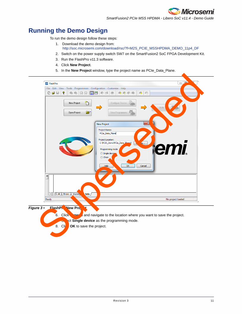
Running the Demo DesignTo run the demo design follow these steps:
1. Download the demo design from: http://soc.microsemi.com/download/rsc/?f=M2S_PCIE_MSSHPDMA_DEMO_11p4_DF
2. Switch on the power supply switch SW7 on the SmartFusion2 SoC FPGA Development Kit.
3. Run the FlashPro v11.3 software.
4. Click New Project.
5. In the New Project window, type the project name as PCIe_Data_Plane.
6. Click Browse and navigate to the location where you want to save the project.
7. Select Single device as the programming mode.
8. Click OK to save the project.
Figure 3 • FlashPro New Project
Supers
eded
PCIe Data Plane Demo Using MSS HPDMA
12 Revis ion 3
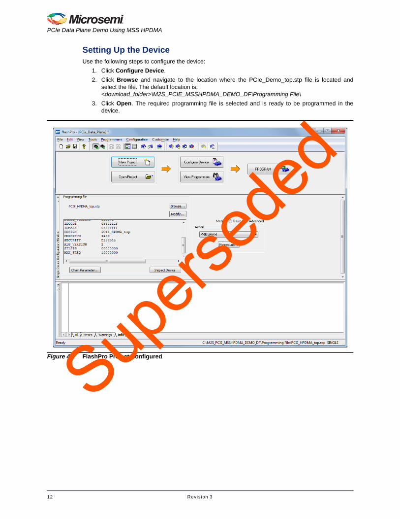
Setting Up the DeviceUse the following steps to configure the device:
1. Click Configure Device.
2. Click Browse and navigate to the location where the PCIe_Demo_top.stp file is located andselect the file. The default location is: <download_folder>\M2S_PCIE_MSSHPDMA_DEMO_DF\Programming File\
3. Click Open. The required programming file is selected and is ready to be programmed in thedevice.
Figure 4 • FlashPro Project ConfiguredSupers
eded
SmartFusion2 PCIe MSS HPDMA - Libero SoC v11.4 - Demo Guide
Revis ion 3 13
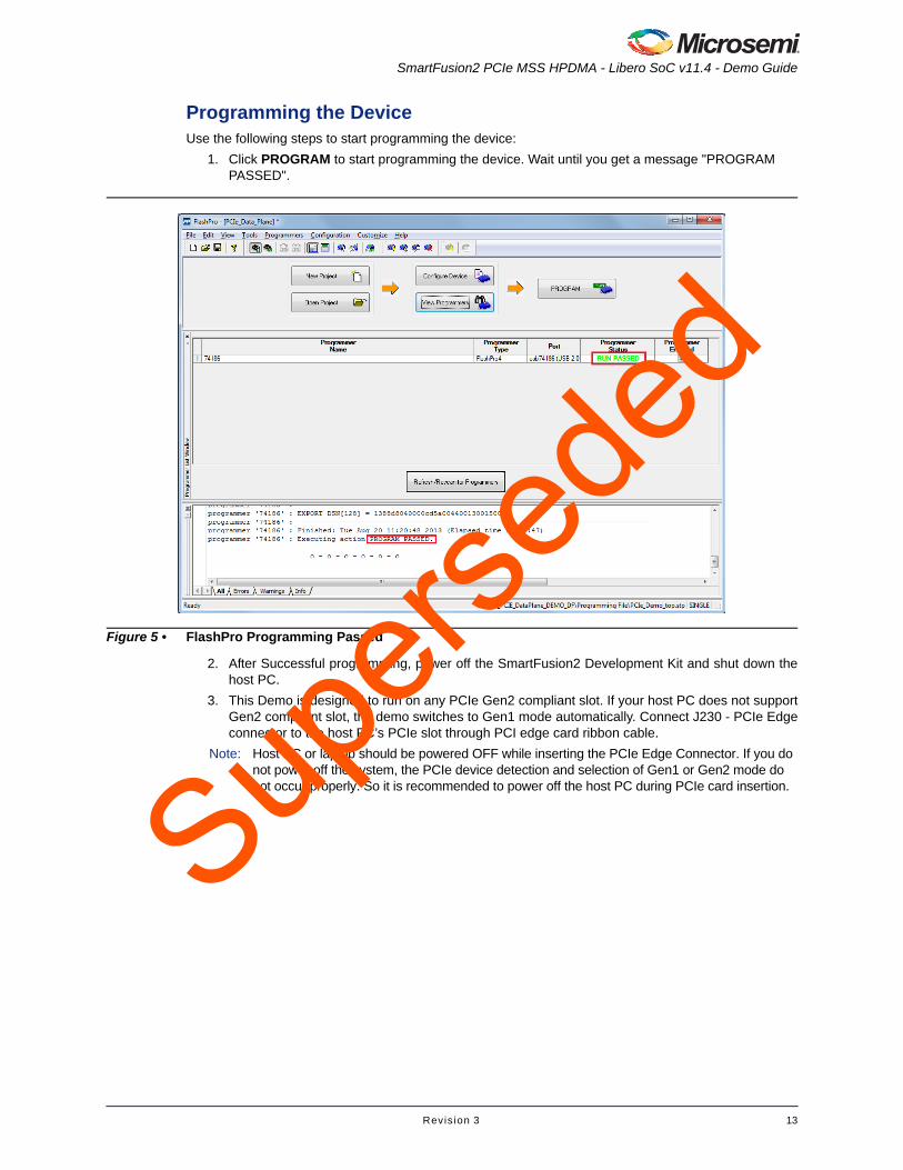
Programming the DeviceUse the following steps to start programming the device:
1. Click PROGRAM to start programming the device. Wait until you get a message "PROGRAM PASSED".
2. After Successful programming, power off the SmartFusion2 Development Kit and shut down thehost PC.
3. This Demo is designed to run on any PCIe Gen2 compliant slot. If your host PC does not supportGen2 compliant slot, the demo switches to Gen1 mode automatically. Connect J230 - PCIe Edgeconnector to the host PC’s PCIe slot through PCI edge card ribbon cable.
Note: Host PC or laptop should be powered OFF while inserting the PCIe Edge Connector. If you do not power off the system, the PCIe device detection and selection of Gen1 or Gen2 mode do not occur properly. So it is recommended to power off the host PC during PCIe card insertion.
Figure 5 • FlashPro Programming Passed
Supers
eded

PCIe Data Plane Demo Using MSS HPDMA
14 Revis ion 3
4. The board setup is shown in Figure 6.
5. Switch the power supply switch SW7 to ON position.
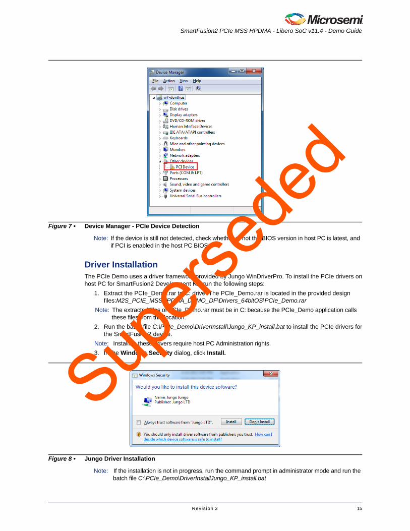
6. Power on the host PC and check the host PC’s Device Manager for PCIe Device. It will besimilar to Figure 7. If the device is not detected, power cycle the SmartFusion2 Development Kitand click “scan for hardware changes” (as shown in Figure 12 on page 17) in Device Manager.If the host PC has any other installed drivers (previous versions of Jungo drivers) for theSmartFusion2 PCIe device, uninstall them and make sure that the PCI Device is displayed in theDevice Manager window as shown in Figure 7.
Figure 6 • SmartFusion2 Development Kit Setup
Supers
eded
SmartFusion2 PCIe MSS HPDMA - Libero SoC v11.4 - Demo Guide
Revis ion 3 15
Note: If the device is still not detected, check whether or not the BIOS version in host PC is latest, and if PCI is enabled in the host PC BIOS.
Driver InstallationThe PCIe Demo uses a driver framework provided by Jungo WinDriverPro. To install the PCIe drivers onhost PC for SmartFusion2 Development Kit, run the following steps:
1. Extract the PCIe_Demo.rar to C: drive. The PCIe_Demo.rar is located in the provided design files:M2S_PCIE_MSSHPDMA_DEMO_DF\Drivers_64bitOS\PCIe_Demo.rar
Note: The extracted files of PCIe_Demo.rar must be in C: because the PCIe_Demo application calls these files from this location.
2. Run the batch file C:\PCIe_Demo\DriverInstall\Jungo_KP_install.bat to install the PCIe drivers forthe SmartFusion2 device.
Note: Installing these drivers require host PC Administration rights.
3. In the Windows Security dialog, click Install.
Note: If the installation is not in progress, run the command prompt in administrator mode and run the batch file C:\PCIe_Demo\DriverInstallJungo_KP_install.bat
Figure 7 • Device Manager - PCIe Device Detection
Figure 8 • Jungo Driver Installation
Supers
eded

PCIe Data Plane Demo Using MSS HPDMA
16 Revis ion 3
4. Click Install this driver software anyway if the window appears as shown in Figure 9.
Demo GUISmartFusion2 PCIe Demo GUI is a simple GUI that runs on the host PC to communicate with theSmartFusion2 PCIe endpoint device. The GUI provides PCIe link status, driver information, and democontrols to perform the DMA transactions to observe the data throughputs. GUI invokes the PCIe driverinstalled on the host PC and provides commands to the driver according to the selection made.
To install the GUI, use the following steps:
1. Extract the PCIe_Demo_GUI_Installer.rar to C: drive. The PCIe_Demo_GUI_Installer.rar is located in the provided design files: M2S_PCIE_MSSHPDMA_DEMO_DF/GUI.
2. Double click setup.exe (PCIe_Demo_GUI_Installer/setup.exe). Apply default options and click Next to complete the installation as shown in Figure 10.
Figure 9 • Windows Security
Figure 10 • GUI Installation
Supers
eded

SmartFusion2 PCIe MSS HPDMA - Libero SoC v11.4 - Demo Guide
Revis ion 3 17
3. After successful installation the following window is displayed.
4. Shut down the host PC.
5. Power-Cycle the SmartFusion2 Development Kit board.
6. Restart the host PC.
Steps to Run the Design1. Check the host PC Device Manager for the drivers. It will be similar to Figure 12. If the device is
not detected, power cycle the SmartFusion2 Development Kit and click “scan for hardware changes” in Device Manager.
Figure 11 • Successful Installation of GUI
Figure 12 • Device Manager - PCIe Device Detection
Supers
eded

PCIe Data Plane Demo Using MSS HPDMA
18 Revis ion 3
Note: If a warning symbol appears on the Device or WinDriver icons in Device Manager, uninstall them and start from step1 of driver installation.
2. Invoke the GUI from ALL Programs > PCIe_Demo > PCIe Demo GUI. The GUI is displayed asshown in Figure 13.
Figure 13 • PCIe Demo GUI
Supers
eded
SmartFusion2 PCIe MSS HPDMA - Libero SoC v11.4 - Demo Guide
Revis ion 3 19
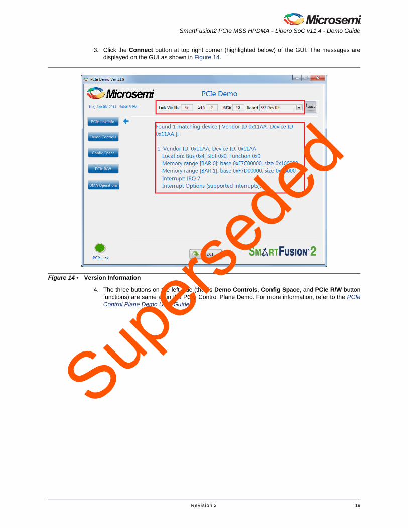
3. Click the Connect button at top right corner (highlighted below) of the GUI. The messages aredisplayed on the GUI as shown in Figure 14.
4. The three buttons on the left side (that is Demo Controls, Config Space, and PCIe R/W buttonfunctions) are same as in the PCIe Control Plane Demo. For more information, refer to the PCIeControl Plane Demo User Guide.
Figure 14 • Version Information
Supers
eded

PCIe Data Plane Demo Using MSS HPDMA
20 Revis ion 3
5. Click DMA Operations. The controls are displayed as shown in Figure 15.
The controls in the box marked with 1 are related to DMA operations. The transfer size (as shown in Figure 16 on page 21) can be selected from 64 KB to 1 MB for:
• PC memory to DDR3
• DDR3 to PC memory
The transfer size is provided in steps of HPDMA buffer descriptor size (64 KB). For moreinformation on buffer description, refer to the "HPDMA" chapter in the SmartFusion2Microcontroller Subsystem User Guide.
The Transfer Size can be selected from 16 KB to 128 KB for:
• Fabric LSRAM to DDR3
• DDR3 to Fabric LSRAM
Figure 15 • DMA Operations
Supers
eded
SmartFusion2 PCIe MSS HPDMA - Libero SoC v11.4 - Demo Guide
Revis ion 3 21
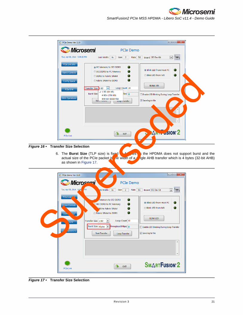
6. The Burst Size (TLP size) is fixed to 4 bytes as the HPDMA does not support burst and theactual size of the PCIe packet is the width of a single AHB transfer which is 4 bytes (32-bit AHB)as shown in Figure 17.
Figure 16 • Transfer Size Selection
Figure 17 • Transfer Size Selection
Supers
eded

PCIe Data Plane Demo Using MSS HPDMA
22 Revis ion 3
7. Select the type of DMA transfer as PC Memory to SF2 DDR3, select any Transfer Size and clickStart Transfer as shown in Figure 18. After completion of data transfer, the GUI displays theThroughput in MBps.
8. Enter 10 in the Loop Count box and click Loop Transfer to perform 10 sequential DMAtransactions. The PCIe_Demo window displays the DMA throughput after completion of datatransfer. Figure 19 shows the throughput of DMA transactions from host PC to DDR3. Theaverage throughput is logged and the log file is stored at C:\PCIe_Demo\DriverInstall in the hostPC.
Figure 18 • PC Memory to DDR3 Transfer Throughput
Supers
eded
SmartFusion2 PCIe MSS HPDMA - Libero SoC v11.4 - Demo Guide
Revis ion 3 23
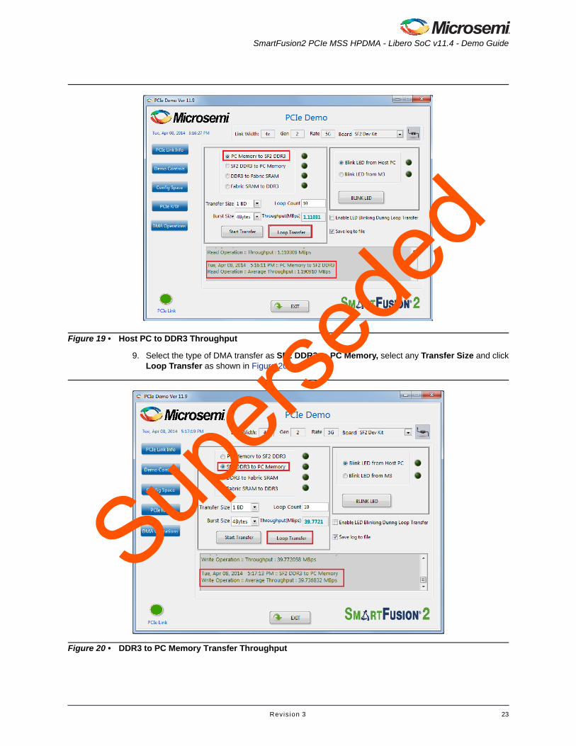
9. Select the type of DMA transfer as SF2 DDR3 to PC Memory, select any Transfer Size and clickLoop Transfer as shown in Figure 20.
Figure 19 • Host PC to DDR3 Throughput
Figure 20 • DDR3 to PC Memory Transfer Throughput
Supers
eded

PCIe Data Plane Demo Using MSS HPDMA
24 Revis ion 3
10. Select the type of DMA transfer as DDR3 to Fabric SRAM, select any Transfer Size and clickLoop Transfer as shown in Figure 21.
11. Select the type of DMA transfer as Fabric SRAM to DDR3, select any Transfer Size and clickLoop Transfer as shown in Figure 22.
Figure 21 • DDR3 to Fabric SRAM Transfer Throughput
Figure 22 • Fabric SRAM to DDR3 Transfer Throughput
Supers
eded

SmartFusion2 PCIe MSS HPDMA - Libero SoC v11.4 - Demo Guide
Revis ion 3 25
12. The LEDs on the board can be blinked in parallel to the DMA operations by using the LEDcontrols on the right side of GUI. The Do DMA transfer and LED toggle check box need to beselected to do the LED blinking from host PC and DMA transfers.
13. Click Exit to quit the demo.
SummaryThis demo shows how to implement a PCIe data plane design using MSS HPDMA. Data transfer occursbetween PCIe, SmartFusion2 LSRAM and SmartFusion2 DDR. Throughput for data transfers isdependent on host PC system configuration, type of PCIe slots used.
Table 3 shows the throughput values observed on the HP Workstation Z220 - CMT.
Table 3 • Throughput Summary
DMA Transfer Type
DMA Transfer Size
Throughput (M Bytes Per Second)
Gen 1 Gen 2
Single Transfer Loop Transfer Single Transfer Loop Transfer
Host PC Memory to DDR3
1 BD (64KB)/
4 BD (256KB)/ 4x4 BD (1MB)
2.3 2.1 2.4 2.1
DDR3to Host PC Memory
1 BD (64KB)/
4 BD (256KB)/ 4x4 BD (1MB)
25 25 39 39
DDR3 to Fabric SRAM
16KB/ 32KB/ 64KB/ 128KB
97 97 97 97
Fabric SRAM to DDR3
16KB/ 32KB/ 64KB/ 128KB
99 99 99 99
Supers
eded

Revision 3 26
A – List of Changes
The following table lists the critical changes that were made in each revision of the chapter in the demo guide.
Date Changes Page
Revision 3(August 2014)
Updated the document for Libero v11.4 software release (SAR 59739). NA
Revision 2(April 2014)
Updated the document for Libero v11.3 software release (SAR 56582). NA
Revision 1(November 2013)
Updated the document for Libero v11.2 software release (SAR 52901). NA
Revision 0(September 2013)
Initial Release NA
Supers
eded

Revision 3 27
B – Product Support
Microsemi SoC Products Group backs its products with various support services, including CustomerService, Customer Technical Support Center, a website, electronic mail, and worldwide sales offices.This appendix contains information about contacting Microsemi SoC Products Group and using thesesupport services.
Customer ServiceContact Customer Service for non-technical product support, such as product pricing, product upgrades,update information, order status, and authorization.
From North America, call 800.262.1060From the rest of the world, call 650.318.4460Fax, from anywhere in the world, 408.643.6913
Customer Technical Support CenterMicrosemi SoC Products Group staffs its Customer Technical Support Center with highly skilledengineers who can help answer your hardware, software, and design questions about Microsemi SoCProducts. The Customer Technical Support Center spends a great deal of time creating applicationnotes, answers to common design cycle questions, documentation of known issues, and various FAQs.So, before you contact us, please visit our online resources. It is very likely we have already answeredyour questions.
Technical SupportVisit the Customer Support website (www.microsemi.com/soc/support/search/default.aspx) for more information and support. Many answers available on the searchable web resource include diagrams, illustrations, and links to other resources on the website.
WebsiteYou can browse a variety of technical and non-technical information on the SoC home page, at www.microsemi.com/soc.
Contacting the Customer Technical Support CenterHighly skilled engineers staff the Technical Support Center. The Technical Support Center can becontacted by email or through the Microsemi SoC Products Group website.
EmailYou can communicate your technical questions to our email address and receive answers back by email,fax, or phone. Also, if you have design problems, you can email your design files to receive assistance.We constantly monitor the email account throughout the day. When sending your request to us, pleasebe sure to include your full name, company name, and your contact information for efficient processing ofyour request.
The technical support email address is [email protected].
Supers
eded

Product Support
28 Revision 3
My CasesMicrosemi SoC Products Group customers may submit and track technical cases online by going to My Cases.
Outside the U.S.Customers needing assistance outside the US time zones can either contact technical support via email([email protected]) or contact a local sales office. Sales office listings can be found atwww.microsemi.com/soc/company/contact/default.aspx.
ITAR Technical SupportFor technical support on RH and RT FPGAs that are regulated by International Traffic in Arms Regulations (ITAR), contact us via [email protected]. Alternatively, within My Cases, select Yes in the ITAR drop-down list. For a complete list of ITAR-regulated Microsemi FPGAs, visit the ITAR web page.
Supers
eded

50200501-3/08-14
© 2014 Microsemi Corporation. All rights reserved. Microsemi and the Microsemi logo are trademarks ofMicrosemi Corporation. All other trademarks and service marks are the property of their respective owners.
Microsemi Corporate HeadquartersOne Enterprise, Aliso Viejo CA 92656 USAWithin the USA: +1 (800) 713-4113 Outside the USA: +1 (949) 380-6100Sales: +1 (949) 380-6136Fax: +1 (949) 215-4996E-mail: [email protected]
Microsemi Corporation (Nasdaq: MSCC) offers a comprehensive portfolio of semiconductorand system solutions for communications, defense and security, aerospace, and industrialmarkets. Products include high-performance and radiation-hardened analog mixed-signalintegrated circuits, FPGAs, SoCs, and ASICs; power management products; timing andsynchronization devices and precise time solutions, setting the world's standard for time; voiceprocessing devices; RF solutions; discrete components; security technologies and scalableanti-tamper products; Power-over-Ethernet ICs and midspans; as well as custom designcapabilities and services. Microsemi is headquartered in Aliso Viejo, Calif. and hasapproximately 3,400 employees globally. Learn more at www.microsemi.com.
Supers
eded