Lesson 8: Component Placement - EMA iTrain...
45
8 December, 2012 OrCAD PCB Editor - Version 16.6 8-1 Lesson 8: Component Placement Learning Objectives In this lesson you will: • Using floorplanning to organize the placement of components with the same ROOM property • Assign reference designators to preplaced parts • Interactively place components using various commands In this section you will place components on your board. You will learn how to create Rooms and assign components to rooms, how to assign reference designators to preplaced symbols, and how to quickly place components. You will also learn the interactive commands available when working with placement. 273
Transcript of Lesson 8: Component Placement - EMA iTrain...

8
December, 2012 OrCAD PCB Editor - Version 16.6 8-1
Lesson 8: Component Placement
Learning Objectives
In this lesson you will:
• Using floorplanning to organize the placement of components with the same ROOM property
• Assign reference designators to preplaced parts
• Interactively place components using various commands
In this section you will place components on your board. You will learn how to create Rooms and assign components to rooms, how to assign reference designators to preplaced symbols, and how to quickly place components. You will also learn the interactive commands available when working with placement.
273

Component Placement Lesson 8
8-2 OrCAD PCB Editor - Version 16.6 December, 2012
Design Layout Process
This design flow is used throughout the entire course. Each box in this flow represents a common step in the design of a printed circuit board. As indicated in the flow, the Arrange/place components feature will now be discussed.
274

December, 2012 OrCAD PCB Editor - Version 16.6 8-3
Lesson 8 Component Placement
Placement Prerequisites
It is important to remember how OrCAD and Allegro PCB Editor determines where the footprints and padstacks are located on disk. The variables PSMPATH and PADPATH are used to determine the locations on disk of the footprints and padstacks, respectively. These variables are defined in the env file and can also be set and modified using the User Preferences Editor.
The prerequisites for manual placement are:
– Symbols: The package symbols and padstacks required for parts in the netlist must exist. Again, the PSMPATH and the PADPATH point to the locations of the symbols and padstacks.
– Netlist: You must load a schematic database into a OrCAD and Allegro PCB Editor design file.
– Alternate Package Symbols: If you plan to select alternative package symbols during manual placement, the alternate symbol definitions must be contained in the appropriate part definition files.
– Floorplanning: You can create a “block diagram” of the logical functions that need to be arranged on the board by using Rooms. Specify this part property within the schematic environment.
– Package Keepouts: If your master design file did not contain package keepouts, add them before you begin placing components, by selecting Setup - Areas - Package Keepout. This step is also optional.
275

Component Placement Lesson 8
8-4 OrCAD PCB Editor - Version 16.6 December, 2012
Placement Edit Application Mode
The Placement application mode is a tuned, high performance environment designed to increase efficiency during component placement sessions. Find filter settings are limited to those elements typically involved in placement such as symbols, pins and rat tees. This reduces unnecessary cycling of unwanted elements that do not contribute towards placement activity. In this mode, it is still possible to perform non-placement function like add connect or slide. However, context sensitive and auto executed commands are biased towards component placement functions.
The list of unplaced components is listed in the Options window. This form is an abbreviated version of the place manual user interface. You can toggle on the Mirror option so that all parts placed are automatically mirrored to the opposite side of the board. The Place by refdes field is used to enter in reference designators. Wildcard characters of “*” and “?” are accepted in this field.
The More options button launches a form that is almost identical to the place manual form. You can use this form to further refine the parts that are selected to be placed. Upon selecting the OK button in this form, the parts populated in the Options window will be updated.
276

December, 2012 OrCAD PCB Editor - Version 16.6 8-5
Lesson 8 Component Placement
Placement Grid
The grid used for placement is the Non-Etch grid. The origin of the package symbol which is defined during symbol creation, snaps to the Non-Etch grid when placing parts with your mouse.
Select Setup - Grids or the Setup - Design Parameters - Display tab - Setup Grids to set the spacing for manual placement on the Non-Etch grid. The origin of the placement grid is the origin of the OrCAD and Allegro PCB Editor design file. Use the Grid form to toggle the grid visibility ON or OFF.
You can also use the Grid Toggle icon to turn the grid display ON or OFF.
Remember, you can use the “x” command to place a part in your design that does not align with the grid, such as connectors.
277

Component Placement Lesson 8
8-6 OrCAD PCB Editor - Version 16.6 December, 2012
Strategy
1. Floorplanning: You can create a “block diagram” of the logical functions through the use of Rooms.
2. Assign fixed IO devices: Use the Logic -Assign RefDes command to correlate any connector package symbols (mechanically placed within the master or template file) to reference designators in the database (such as P1, J2). This process also applies to any mechanically constrained devices preplaced in the master design file (such as LEDs).
3. Place IO bound devices: Place any parts that send or receive nets from backplane connectors to minimize overall net length.
4. Place critical logic functions: Place clock circuits, memory arrays, buffers, controllers, and address buses. (See Floorplanning on the next page.)
5. Place less critical circuits: Place data buses and random logic, interactively or automatically.
6. Evaluate and revise placement: Use ratsnest display, net highlighting, interactive or automatic gate and pin swapping, density evaluations, interactive net scheduling, DFA, and Signal Analysis tools.
278

December, 2012 OrCAD PCB Editor - Version 16.6 8-7
Lesson 8 Component Placement
7. Place bulk decoupling caps: Perform this step last. If embedded split planes are required for multiple voltages, group filter caps and associated ICs accordingly.
NoteSome database reports may be useful during the placement process (for example, nets list, components list, bill of materials, and placed or unplaced components list). Also, you can use Etch Length by Net Report to flag potential net length problems prior to routing.
Floorplanning with Rooms
Rooms are confinement areas that provide a useful method of grouping components. You can force automatic placement to occur with specific components and cause them to be placed within specific rooms. You can attach a room property to components during schematic creation, netlist creation, or at any time while in the OrCAD and Allegro PCB Editor design. Room boundaries are recognized as being closed polygons on the TOP_ROOM, BOTTOM_ROOM, or BOTH_ROOMS subclasses of the BOARD GEOMETRY class.
279

Component Placement Lesson 8
8-8 OrCAD PCB Editor - Version 16.6 December, 2012
Creating a Room
Use this Room Outline form to add rooms to your board for component placement.
Command Operations:
– Create: Allows you to create a new room.
– Edit: Edits an existing room.
– Move: Moves an existing room.
– Delete: Allows you to delete a room.
Room Name Area:
– Name: When Create is active, names a new room. When active in Edit, Move or Delete, selects from a drop-down list of available rooms. This room name must match the property name given to the symbols.
Side of Board:
– Top, Bottom, Both: Defines which side of the board the room will be created.
Room Properties (the package boundary of the part is used for checking purposes)
280

December, 2012 OrCAD PCB Editor - Version 16.6 8-9
Lesson 8 Component Placement
– Hard: DRCs are created when a part belonging to the room is not placed entirely within the boundary or if a part not belonging to the room is placed within the room.
– Soft: No DRC errors are ever created. Use this option as a guide for placement.
– Inclusive: Like HARD, but allows components with different ROOM names to be placed in the room without a DRC.
– Hard Straddle: Like HARD, but components may straddle the room boundary.
– Inclusive Straddle: Any components may be placed in the room or straddle the boundary. A DRC will be generated only when a component with a room name is placed completely outside of the room.
– Design Level: Controls behavior for all rooms in the design without an assigned ROOM_TYPE property, using the same values as above. If no ROOM_TYPE property is found for a room, then SOFT behavior is used.
Create/Edit options:
– Draw Rectangle: Allows you to create and size a rectangle.
– Place Rectangle: Allows you to create a rectangle per your specified dimensions.
– Draw Polygon: Allows you to create a polygon.
While in Edit mode:
– Available room area used: shows the percentage of the area that the components will require.
– Autosize: Automatically resizes the selected room to the percent specified.
281
Component Placement Lesson 8
8-10 OrCAD PCB Editor - Version 16.6 December, 2012
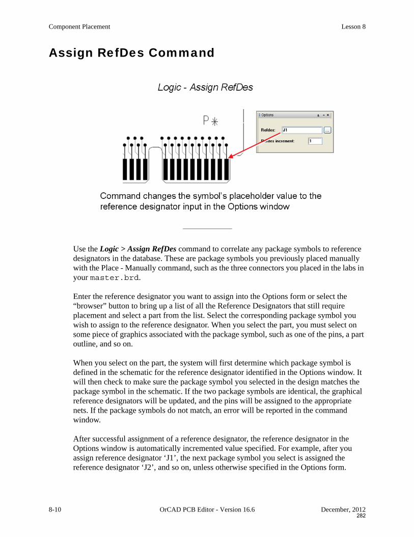
Assign RefDes Command
Use the Logic > Assign RefDes command to correlate any package symbols to reference designators in the database. These are package symbols you previously placed manually with the Place - Manually command, such as the three connectors you placed in the labs in your master.brd.
Enter the reference designator you want to assign into the Options form or select the “browser” button to bring up a list of all the Reference Designators that still require placement and select a part from the list. Select the corresponding package symbol you wish to assign to the reference designator. When you select the part, you must select on some piece of graphics associated with the package symbol, such as one of the pins, a part outline, and so on.
When you select on the part, the system will first determine which package symbol is defined in the schematic for the reference designator identified in the Options window. It will then check to make sure the package symbol you selected in the design matches the package symbol in the schematic. If the two package symbols are identical, the graphical reference designators will be updated, and the pins will be assigned to the appropriate nets. If the package symbols do not match, an error will be reported in the command window.
After successful assignment of a reference designator, the reference designator in the Options window is automatically incremented value specified. For example, after you assign reference designator ‘J1’, the next package symbol you select is assigned the reference designator ‘J2’, and so on, unless otherwise specified in the Options form.
282

December, 2012 OrCAD PCB Editor - Version 16.6 8-11
Lesson 8 Component Placement
Labs
• Lab 8-1: Floorplanning
– Organize areas of the board to place component parts with the same ROOM property together on the board
– Set the non-etch grid
– Add rooms
– Add room text
• Lab 8-2: Assigning Preplaced Packages
– Associate a preplaced component with a logical part from the netlisted database
The following labs will allow you to:
• Familiarize yourself with the process required to create rooms within your design.
• Familiarize yourself with the process required to assign reference designators to preplaced packages.
283

Component Placement Lesson 8
8-12 OrCAD PCB Editor - Version 16.6 December, 2012
Lab 8-1: FloorplanningObjective: Create a floorplan by adding four rooms for component
placement.
Each design has unique placement requirements. For this reason, floorplanning is performed after the logic has been loaded into the master design file.
Starting in the Work Directory
Later in this module, you will perform pin and gate swapping. Pin and gate swapping is an operation that can change your design, making it no longer synchronous with the original schematic. In this case, you will need to run backannotation. We cover backannotation later.
1. Start the OrCAD and Allegro PCB Editor.
2. Choose File - Open and open the constraints.brd design (if it is not the current design).
3. Use the View - Zoom Fit command to fit the board to your work area.
Setting the Non-Etch Grid
During placement, components you move will lock to this grid.
1. Toggle the grid points to ON, if they are not currently displayed, by clicking the Grid icon in the top menu.
2. Choose Setup - Grids.
The Define Grid form opens.
284

December, 2012 OrCAD PCB Editor - Version 16.6 8-13
Lesson 8 Component Placement
3. Locate the Non-Etch section at the top of the form and set the X and Y Spacing to 25 mils, as shown in the figure:
4. Click OK at the bottom of the form.
You might see the following message:
“Grids are drawn at 100.0, 100.0 apart for enhanced viewability.”
In this case, you need to zoom in to actually see the 25-mil grid points.
Adding Rooms
In the following exercise, you first turn on the layers that display the room information. You will add four rectangular rooms and give them each a name. Each set of coordinate points you enter becomes the diagonal corner of a rectangle.
1. Click the Color192 icon.
The Color Dialog form appears.
2. Select the BOARD GEOMETRY folder.
3. Toggle the TOP_ROOM and the BOTH_ROOMS subclasses ON. If you prefer a different color for these subclasses, you can also set the color at this time.
4. Click OK to close the Color Dialog form.
5. Choose Setup - Outlines - Room Outline from the top menu.
285

Component Placement Lesson 8
8-14 OrCAD PCB Editor - Version 16.6 December, 2012
The Room Outline form displays. Set the form to appear as shown:
NoteDo NOT click OK in this form until you have completed creating all of your rooms. The OK button closes out this command.
6. At the OrCAD and Allegro PCB Editor command line, enter:
x 1300 1500
x 3900 700
NoteThis creates a CHAN1 room where the components that have the Component property ROOM=CHAN1 will be placed. When ROOM_TYPE = Inclusive Straddle is set and these parts are placed outside of the assigned room, a DRC flag will be shown until the problem is resolved.
7. If it is not already, change the Room Name to CHAN2 and enter:
x 1300 700
x 3900 -100
8. Use the down arrow and change the Room Name to MEM and enter:
x 1900 4225
x 3900 2200
9. Change the Side of Board to Top.
286

December, 2012 OrCAD PCB Editor - Version 16.6 8-15
Lesson 8 Component Placement
10. Change the Room Name to LED and enter:
x 1400 2200
x 3900 1500
Four rectangles appear on the board with the labels attached to them.
11. Click OK to get out of the form.
You have just created four rooms - the CHAN1, CHAN2, MEM and LED rooms. Components that have an attached Room property equal to these name values will be placed according to the room they belong in.
12. Choose File - Save from the top menu.
A window appears and warns you that the constraints.brd file already exists. It asks if you want to overwrite the file.
13. Click Yes to confirm the overwrite.
The file constraints.brd is written to disk.
End of LabSTOPSTOP
287

Component Placement Lesson 8
8-16 OrCAD PCB Editor - Version 16.6 December, 2012
Lab 8-2: Assigning Preplaced PackagesObjective: Associate preplaced connectors to the logical database.
The mechanical template used to create this design file (master.brd) contained preplaced package symbols. In order for a preplaced part to have connectivity, it must be assigned a reference designator that exists in the design database.
1. From the top menu, choose Logic - Assign RefDes.
2. Hover your mouse over the Options foldable window tab to display the window. Click in the Refdes field and enter:
j1
3. Click on any graphics associated with the edge connector symbol on the left side of the design. You may want to zoom in on the connector.
J* has changed to J1.
4. Zoom out to include just the board by selecting the F2 (Zoom - Fit) function key.
Notice in the Options window that J1 has incremented to J2.
5. Click on the upper BNC connector at the right side of the board.
J* has changed to J2.
6. Click on the lower BNC connector at the right side of the board.
288

December, 2012 OrCAD PCB Editor - Version 16.6 8-17
Lesson 8 Component Placement
J* has changed to J3. Both BNC connectors now have reference designators assigned, and any nets of placed pins are displayed, as shown in the figure:
7. Right-click and choose Done from the pop-up menu.
8. Choose File - Save from the top menu.
A window appears and warns you that the constraints.brd file already exists, asking you whether you want to overwrite the file.
9. Click Yes to confirm the overwrite.
The file constraints.brd is written to disk.
End of LabSTOPSTOP
289

Component Placement Lesson 8
8-18 OrCAD PCB Editor - Version 16.6 December, 2012
Placement-Related Properties
The following placement related properties can be placed on your components at either the board design stage or the schematic capture environment to control their placeability or swapability.
• ROOM — Indicates that the component is to be located in a particular location, identified by the room name, during automatic placement.
• NO_SWAP_GATE — Indicates that functions (slots or gates) within a component cannot be swapped.
• NO_SWAP_GATE_EXT — This function (slot or gate) cannot be swapped with a function (slot or gate) from another component (only swapped among slots or gates within its current component).
• NO_SWAP_PIN — Indicates that pins on this component or function (slot or gate) cannot be swapped, either interactively or automatically.
• FIX_ALL — Declares that components having this property will not be eligible for any pin or function (slot or gate) swapping.
• FIXED — Component cannot be moved or deleted.
290

December, 2012 OrCAD PCB Editor - Version 16.6 8-19
Lesson 8 Component Placement
Placement Commands
OrCAD and Allegro PCB Editor placement commands include the following types that will be discussed in this class:
• Manual placement commands are used to select components individually or by groups, and interactively determine their location.
• Quickplace is an automatic placement command which will automatically place parts outside the board outline and place part inside their designated rooms. Then the parts can be placed interactively to determine their final location.
• Swap (interactive) allows functions to be relocated to same or different packages to aid in routing strategies.
• Component symbol utilities include methods of accessing new library data to update your design.
291
Component Placement Lesson 8
8-20 OrCAD PCB Editor - Version 16.6 December, 2012
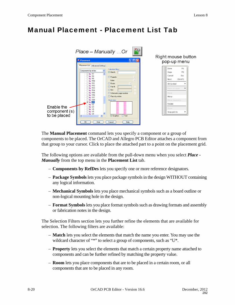
Manual Placement - Placement List Tab
The Manual Placement command lets you specify a component or a group of components to be placed. The OrCAD and Allegro PCB Editor attaches a component from that group to your cursor. Click to place the attached part to a point on the placement grid.
The following options are available from the pull-down menu when you select Place - Manually from the top menu in the Placement List tab.
– Components by RefDes lets you specify one or more reference designators.
– Package Symbols lets you place package symbols in the design WITHOUT containing any logical information.
– Mechanical Symbols lets you place mechanical symbols such as a board outline or non-logical mounting hole in the design.
– Format Symbols lets you place format symbols such as drawing formats and assembly or fabrication notes in the design.
The Selection Filters section lets you further refine the elements that are available for selection. The following filters are available:
– Match lets you select the elements that match the name you enter. You may use the wildcard character of “*” to select a group of components, such as “U*.
– Property lets you select the elements that match a certain property name attached to components and can be further refined by matching the property value.
– Room lets you place components that are to be placed in a certain room, or all components that are to be placed in any room.
292

December, 2012 OrCAD PCB Editor - Version 16.6 8-21
Lesson 8 Component Placement
– Part # lets you place components with the given part number. The wild card character can be used.
– Net lets you place all components that have a given net assigned to one of the pins of the part. The wild card character can be used.
– Schematic page number allows you to place all the parts on a particular page.
– Place by refdes changes the Quickview section of the form where you can select components by class (IC, IO, Discrete, Mechanical), by the Place tag property, or by device type. There is also a section where you can specify parts based upon minimum and maximum number of pins.
While a part is attached to the cursor, click right to access options for rotating the part, or mirroring the part to the opposite side.
Manual Placement - Advanced Settings Tab
By default, the Manual Placement form will be displayed at all times. Here is the definition of the various options in the Advanced Settings tab.
• List Construction - Display definitions from: Lets you choose from where symbol and module definitions are displayed: the database of the current design, the libraries, or both
• Symbols and Module Definitions
– AutoNext
293

Component Placement Lesson 8
8-22 OrCAD PCB Editor - Version 16.6 December, 2012
• Enabled: (Default) Makes the next symbol in your placement list available for placing without the need to choose Next from the pop-up menu. When you are in this mode, choosing Next puts the next element on the cursor without placing the current one.
• Disable: Requires you to choose Next from the pop-up menu to make the next element on the list available for placement. In this mode, the component on the cursor is moved with every new pick and an instance of a non-component symbol on the cursor is placed at each new pick until Next is chosen.
The behavior of AutoNext differs somewhat when placing non-component symbols or module definitions. For these elements, only one copy of the element is placed when AutoNext is Enabled.
If AutoNext is disabled, every pick places a copy of the non-component symbol or module until you choose Next from the pop-up. When, however, a component is on the cursor, it remains on the cursor after you place it; subsequent picks unplace the component from its last place location and move it to the next pick location.
– AutoHide - Lets you automatically hide the Placement dialog box once you begin placing elements and re-display it once all elements have been placed. To manually re-display the Placement dialog box, right-click and choose Show.
• Modules net exception list - Lets you create or use an existing exception list for renaming nets when you are about to place a module instance previously created in your design. When a module is added to a design, all components and nets in the module are given unique names so that they do not conflict with any other design objects already present.
– File - In most designs, you want to make an exception to this general rule in the case of power and ground nets, which you would normally want to merge with the design. The nets you want to merge with the existing board can be added to a module net exception list, an ASCII file containing net names that is not changed when a module is added to the design. You specify this file in this field. You can either enter the list file name or use the Browse button to locate the file.
– Create - Creates list files and brings up the Select Nets dialog box from which you can create an exception list. You can also create list files typing them in with an external text editor or by using the define list command.
• OK - Saves any changes made during the session and closes the dialog box.
• Hide - Causes the Placement dialog box to disappear. To re-display the Placement dialog box, choose Show from the pop-up menu.
294

December, 2012 OrCAD PCB Editor - Version 16.6 8-23
Lesson 8 Component Placement
Changing the Default Orientation
When you place parts manually, they are by default placed as created in the library. If you want to start placing parts at a different angle, rather than using the Right-Mouse-Button pop-up Rotate command and then spinning the part, you can change the default orientation for the parts attached to your cursor. Use Setup - Design Parameters, go to the Design folder tab and change the Angle field to the desired rotation. You can change the rotation to any of those available in the pull-down, or you can type in any value you need.
By default, all parts are placed on the top side of the board. However, certain times you may want to place a series of parts on the bottom or back side of the design, such as standard surface-mount decoupling capacitors. To have OrCAD and Allegro PCB Editor place each part on the bottom side of the board, WITHOUT manually using the Right-Mouse-Button pop-up “mirror” option, set the Mirror toggle in the Design folder tab under Setup - Design Parameters. After you set this toggle, all parts that are manually placed will by default be placed on the bottom side of the board.
This function has been added to the Options foldable window when in the Placement Edit application mode.
295

Component Placement Lesson 8
8-24 OrCAD PCB Editor - Version 16.6 December, 2012
Lab
• Lab 8-3: Manual Placement
– Place parts by reference designator
– Change default orientation
– Use the Move and Rotate commands
– Move groups of parts
The following lab will allow you to familiarize yourself with the process required to manually place parts on the board. You will learn how to rotate parts, mirror parts, move parts and other manual placement options.
296

December, 2012 OrCAD PCB Editor - Version 16.6 8-25
Lesson 8 Component Placement
Lab 8-3: Manual PlacementObjective: Select, place, and move components interactively until all the
active components have been placed.
Placing Parts by Reference Designator
1. From the top menu, choose Setup - Application Mode - Placement Edit.
2. Place your cursor over the foldable Options window to expand it and then dock it in place by clicking on the pushpin icon.
3. In the Place by refdes list scroll through the list and enable the check box to the left of U5.
The OrCAD and Allegro PCB Editor message area states:
Placing U5 / EPF8282A_LCC / PLCC84.
4. Move the cursor into the main OrCAD and Allegro PCB Editor window.
U5 is attached to your cursor. Before placing U5, you need to rotate it.
NoteWhen a part is attached to your cursor for manual placement, it might not be rotated the way you want it placed (0-degree rotation by default). This is the orientation of the part when it was created.
5. Right-click and choose Rotate from the pop-up menu.
A “handlebar” extends between the part and your cursor.
297

Component Placement Lesson 8
8-26 OrCAD PCB Editor - Version 16.6 December, 2012
NoteIf the handlebar does not appear then select Oops from the Right-Mouse-Button and then in the Options window select More Options to open the Placement form. Click the OK button. Now select U5 again from the Components by Refdes listing in the Options window and the handlebar should be available.
6. Use the handlebar to spin the component.
Notice that the angle of rotation appears in the status area at the lower right of your window.
7. Spin U5 to 180 degrees.
Notice the angle reading in the Status area of your screen (to the right of the P and A buttons).
8. When the Status area shows that U5 is in a +180-degree rotation, click left to accept the current orientation.
You are no longer in rotate mode, but you are still in move mode. U5 is still attached to your cursor.
9. Click to place U5 in the design at the location shown in the figure.
10. Right-click and choose Done from the pop-up menu.
298

December, 2012 OrCAD PCB Editor - Version 16.6 8-27
Lesson 8 Component Placement
Coloring the GND and VCC Nets
You might notice when you are interactively placing components that the power and ground nets are not ratsnested. A NO_RAT property is automatically added to the power and ground nets when the logic netlist is read into the database. This is done as a visual aid, assuming that these nets will automatically be routed to their respective internal planes. It is helpful to have these nets set in different colors so you will know where to place the discrete components that are often assigned those nets.
1. Select Display - Color/Visibility in the top menu or select the Color192 icon.
2. In the Color Dialog form select Nets as shown below.
3. Click on a Green chip in the Color palette area - a green color that you haven’t previously used in your color setup.
4. Scroll down the list of nets to find GND.
5. Select in the Net column on the chip for the net GND as shown below.
6. Select a Purple color in the Color palette area.
7. Scroll down the list of nets to find VCC.
8. Select in the Net column on the chip for the net VCC as you did for the GND net.
This will color all the pins, vias, clines, and shapes that are assigned the VCC net in the selected purple color.
299

Component Placement Lesson 8
8-28 OrCAD PCB Editor - Version 16.6 December, 2012
9. Select OK to close the Color Dialog form.
Changing the Default Orientation
Rather than using the Rotate command from the pop-up menu each time you place an individual component, you can override the default orientation using the Design Parameter Editor form.
1. Choose Setup - Design Parameters in the top menu.
2. Click the Design tab to bring it forward.
3. Set the Angle field to 180, as shown:
4. Click OK to exit from the Design Parameter Editor form.
Now the default orientation is 180 degrees (instead of zero).
5. From the Place by refdes list in the Options window, scroll through the list and enable the check box to the left of U1.
6. Move your cursor into the OrCAD and Allegro PCB Editor window.
U1 attaches to your cursor in a 180-degree rotation. The dynamic ratsnest lines appear between the component on your cursor and any currently placed components.
300

December, 2012 OrCAD PCB Editor - Version 16.6 8-29
Lesson 8 Component Placement
7. Click to place the U1 component on the board at the location indicated in the next figure.
8. Place components U3, U4, and U2 using the method you just tried. Refer to the above figure for where to place the components. Do NOT align them up in a straight column or equally space them. In another lab we will use an alignment command to align them equally spaced in a straight column.
Moving Parts
When you are using the Placement Edit application mode or the Place Manually command and no part is selected in the Placement panels, you are by default in the Move mode. You can also at any time initiate the Move mode by using the Right-Mouse-Button and choosing Move.
1. Click to select one of the placed part to moves, and click to place it in a new location.
ImportantWhen selecting parts to move, you must click anywhere on the symbol graphics to identify which one to move.
Place U4 here
Place U3 here
Place U2 here
Place U1 here
301

Component Placement Lesson 8
8-30 OrCAD PCB Editor - Version 16.6 December, 2012
2. Practice this Move command with other parts.
3. Right-click and choose Done from the pop-up menu.
Moving Groups of Parts
1. Choose Edit - Move.
2. In the Find Filter, toggle All Off except Symbols.
3. Click and hold the Left-Mouse-Button as you drag the mouse to stretch a frame around the desired group of components you want to move.
NoteThe graphics of these parts do not need to be entirely within the window to be selected. Do not include any part of the board outline in your selection window. The board outline, keepins, and keepouts were created as one board symbol, so this symbol should NOT be moved.
If you make a mistake creating the selection window, right-click and choose Oops from the pop-up menu. Then use the Left-Mouse-Button to stretch a frame around the desired components.
4. When the parts you want to move are highlighted, click left (but do not hold) to define an origin, or reference point, for the group to move.
The group is attached to the cursor.
5. Move the group around and click on a new grid location to place the group.
6. Right-click and choose Done from the pop-up menu.
7. Save the board as partplaced.brd.
End of LabSTOPSTOP
302

December, 2012 OrCAD PCB Editor - Version 16.6 8-31
Lesson 8 Component Placement
Quickplace
The Quickplace command will place unplaced parts outside the board outline and those parts assigned to a room will be placed inside that room. The command will not place any parts outside the drawing extents. Parts that are already placed in the design will not be affected by the Quickplace command.
Placement Filter
Place by property/value - Place components by their component property and value.
Place by room - Place components into a single room or all rooms simultaneously. If placing components outside the board edge, use Place by property/value.
Place by part number - Place components in groups by part number around the board outline (i.e. 74act32, 74fct244s).
Place by net name - Place components that have a common net name between them. Useful for boards that have multiple voltages and will need to set up placement for a resulting split plane.
Place by schematic page number - When you have a DE HDL (only) schematic, you can place components by page. The Browse button displays the schematic hierarchical blocks or individual pages of sheets that still have unplaced components.
303

Component Placement Lesson 8
8-32 OrCAD PCB Editor - Version 16.6 December, 2012
The Place all components option will attempt to place all currently unplaced parts in the next execution of the command. If this option is not set, the Filters section of the form is enabled.
You use the Place by refdes section to refine the parts for placement. You can use the filters to specify only IC, IO or Discrete components, or any combination of the three. Remember, these three classifications of parts are controlled by the library definition in DE HDL or DE CIS and by the device files for third-party netlists.
Placement Position
By user pick allows you to place anywhere on the drawing. Use in combination with Edge and Board Side.
By using the Edge section and Board Side section of the form, you can control whether parts are placed outside the left, right, top or bottom of the board outline and whether the parts are placed on the top or bottom side of the design. The options can be changed at any time and the command rerun multiple times to achieve almost any desired placement pattern.
The Symbols placed field displays the number of components placed, as well as the number of available components for placement, as determined by the Filters settings.
The Undo last place button will remove only the most recent parts placed, as specified by the Filters setting. The Unplace button will repeatedly remove parts placed for as many times as a place option was run during the current session.
The Unplaced symbol count field displays the current number of parts remaining to be placed.
304

December, 2012 OrCAD PCB Editor - Version 16.6 8-33
Lesson 8 Component Placement
Aligning Components
To maximize channels and printed circuit board real estate, the Placement Edit application mode features the Align Components command. This command is available from the Right-Mouse-Button pop-up menu. This lets you to fine-tune the alignment of already placed components along X, Y, odd angle line, using the following criteria:
• Components must exist on the same subclass
• More than one component must be chosen
• Components must NOT have the FIXED property assigned to them
Steps required to align components:
• Must be in the Placement Edit application mode
• Select all components to be aligned
• Hover your mouse over the reference component
• Use the Right-Mouse-Button pop-up menu option Align Components
• Set the alignment direction, alignment edge, and spacing in the Options foldable window
Alignment Direction - Horizontal or Vertical alignment
305

Component Placement Lesson 8
8-34 OrCAD PCB Editor - Version 16.6 December, 2012
Alignment Edge - When aligning horizontally, select top or bottom as the edge to base alignment on. When aligning vertically, select left or right to base alignment on. Both horizontal and vertical alignments can be base on the symbol centers.
Spacing - The options are Off and Equal Spacing.
• Off - Aligns the components at their current spacing.
• Use DFA Constraints - compresses components in the selection set to the minimum DFA spacing distance (NOT available in the OrCAD PCB Editor.
• Equal Spacing - Uses an algorithm to compute space distances between the first and last component in the selection set then divides by the number of components resulting in an equalized spacing gap between each components. Use the increment/decrement controls to adjust component spacing real time.
306

December, 2012 OrCAD PCB Editor - Version 16.6 8-35
Lesson 8 Component Placement
Deleting Components
There are two different methods to delete a component from a design. Note that when you delete a component, you only unplace the component. Deleting a component does not remove it from the logic, or remove it from the Bill of Material.
One method to delete a component is to use the standard Edit - Delete command. You can delete individual parts from the board or delete a group of components by dragging the mouse and forming a rectangle around a series of parts. Also remember that parts that have the FIXED property will not be deleted.
NoteMake sure to check your Find Filter when attempting to delete parts from your design. If Symbols is not checked, you will not be able to delete the parts desired.
A second method to delete a component is to use the Pre-selection mode. Move your mouse over the part you want to delete and tab through until the Symbol is selected. You can then use the Right-Mouse-Button pop-up menu and select the Unplace component command to delete the part. Note that when you first move your cursor over the part, if the Symbol is not selected, you can use the Right-Mouse-Button pop-up menu, then use the Symbol option, and then select Unplace component.
307

Component Placement Lesson 8
8-36 OrCAD PCB Editor - Version 16.6 December, 2012
Placement Replication
Placement Replication is available in the Placement Application mode environment. The use model requires the preselection of the circuit followed by a Right-Mouse-Button (RMB) action command
To use this functionality, first you must create the original, or seed circuit by placing the desired parts on the board, either using the manual placement commands, or by using Quickplace. If you want to include the etch in the “seed” circuit, add the connections to the parts in the circuit. The seeded circuit can be just one component and its associated etch.
Once the seed circuit has been created, select the components that are the targeted replication groups. You can select components that do not factor into the replicated circuit, which will be ignored, but this may increase processing time.
NoteThe customized positioning of reference designators in the seed circuit will be leveraged across the replicated modules.
Place Replicate Create
To use this functionality, first you must create the original, or seed circuit, by placing the desired parts on the board either using the manual placement commands, or by using Quickplace. If you want to include the etch in the “seed” circuit, add the connections to the parts in the circuit.
308

December, 2012 OrCAD PCB Editor - Version 16.6 8-37
Lesson 8 Component Placement
Select all of the parts in the original placement. Hover your mouse over one of the parts, select with the Right-Mouse-Button - Place Replicate Create from the pop-up menu and the Right-Mouse-Button - Done.
Hover your mouse over a pin in one of the selected components and select with the Right-Mouse-Button - Snap to - Pin. You will be presented a form to name and save the replication circuit either inside the database, or on disk. A file on disk will have the extension .mdd.
Place Replicate Copy
Select the components that are the targeted replication groups. You can select components that do not factor into the replicated circuit, which will be ignored, but this may increase processing time. Once the parts are selected, hover you mouse over one of the selected parts and select with the Right-Mouse-Button - Place Replicate Apply from the popup menu. You can select either a circuit name stored in the database, or from a file previously saved on disk.
If a solution is found, a Place Replicate Component Swap Interface form will appear allowing you to swap out components of similar types. Typically the swappable components are capacitors of different values, resistors of different tolerances, and so on. After picking the swappable parts, select OK in the form and the replicated circuit is attached to your cursor. You can then place the replicated circuit on your design. If more than one circuit can be created from the selected parts, you can place the additional circuits one at a time also.
309

Component Placement Lesson 8
8-38 OrCAD PCB Editor - Version 16.6 December, 2012
Lab
• Lab 8-4: Using Quickplace
– Use the Quickplace command to place parts in the rooms CMEM and CHAN1
– Replicate CHAN1 component placement to CHAN2
– Automatically align the previously placed ICs U1, U3, and U4
– Learn how to use the Delete command to remove and replace board components
The following lab will allow you to:
• Familiarize yourself with the process required to use Quickplace. You will also use the placement skills you have already learned to place the design. Work with the process required to remove and then replace parts in your design.
310

December, 2012 OrCAD PCB Editor - Version 16.6 8-39
Lesson 8 Component Placement
Lab 8-4: Using QuickplaceObjective: Use the Quickplace command to place all the components onto
a partially placed board.
The Quickplace command can be used to place parts on the board and into their assigned rooms.
1. Be sure you are working on the board file partplaced.brd. It is the board we saved in the previous lab.
2. Select View - Zoom Fit the board so such that all of the rooms are visible.
3. If the grids are displayed, turn them off by clicking the Grid Toggle icon.
Quickplacing Components into their Assigned Rooms
First you will quickplace the parts with room assignments into their respective rooms. Then you can start moving parts in the selected rooms to create your final placement.
1. Choose Place - Quickplace from the top menu.
2. In the Quickplace form select the Place by room placement filter and set the room to MEM.
This will flag each component with the MEM Room property and place it in its appropriate room. By default, the Board Side Top was selected as the side of the board that would be placed. So even if the room was defined as BOTH, Quickplace only places one side of the board at a time.
3. Click Place.
This places all the parts with the MEM Room assignment.
4. In the Place by room placement filter and set the room to CHAN1.
This will flag each component with the CHAN1 Room property and place it in its appropriate room.
5. Click Place.
This places all the parts with the CHAN1 Room assignment.
6. Change the Placement Filter from Place by room to Place all components.
311

Component Placement Lesson 8
8-40 OrCAD PCB Editor - Version 16.6 December, 2012
7. If the Edge option is not currently set to Bottom, set it to Bottom now.
8. Click Place.
This places all of the remaining parts along the bottom outer edge of the board.
9. Click OK to close the Quickplace form.
10. You can use the Mirror, Move, Group Move, and Rotate commands to rearrange the locations and orientation of the parts as needed.
CautionBe sure to set your colors so you have visibility of the Package Geometry group, Package Geometry class, Assembly_Top and Assembly_Bottom subclasses. Then under the Component group, set Ref Des class Assembly_Top and Assembly_Bottom subclasses toggled ON. It also will help to have different colors for the different board sides.
11. The final placement location is up to you but we are giving you a suggestion of the MEM room as shown:
NoteRemember to use the Undo and Redo commands available to you.
C15 through C22are mounted onbottom side
312

December, 2012 OrCAD PCB Editor - Version 16.6 8-41
Lesson 8 Component Placement
Here is a placement suggestion for the CHAN1 room.
12. Save the board as partplacedroom.brd file.
Replicate the CHAN 1 Component Placement to CHAN2
1. Zoom In around CHAN1 and CHAN2.
2. Select Setup - Application Mode - Placement Edit.
3. Window select all of the parts in CHAN1 with the exception of the J2 BNC connector.
4. Hover your mouse over one of the pins for L1 and select Right-Mouse-Button - Place replicate create and then Right-Mouse-Button - Done.
5. Hover your mouse over the center pin of J2 and select Right-Mouse-Button - Snap pick to - Pin.
The Pop Dyn_Option_Select form will open.
6. In the File Name field type chan1 and then Save.
7. Reactivate the Placement Edit application mode.
8. Window select all of the parts located along the Bottom edge of the board.
9. Hover your mouse over a pin in the selected parts and select Right-Mouse-Button - Place replicate apply and select chan1.
The Replace Replicate Unmatched Component Interface form will appear displaying the components from CHAN2 matched with those from CHAN1.
10. Click OK in the Replace Replicate Unmatched Component Interface form.
The parts are all attached to your cursor in the replicated stage.
11. Hover your mouse over the center pin of J3 and select RMB - Snap to - Pin.
313

Component Placement Lesson 8
8-42 OrCAD PCB Editor - Version 16.6 December, 2012
The replicated parts in CHAN2 are now placed and aligned with J3 as the ones in CHAN1 are in relations to J2.
12. Using the Edit - Delete command, delete the parts sitting below the bottom edge of the board.
The components are highlighted, giving you a chance to verify that these are the components you really want to delete. If you made a mistake, at this point you could choose Oops from the pop-up menu.
13. Click again anywhere on the board or select Right-Mouse-Button - Done to delete them.
The components are deleted from the board, but not from the component database. They are placed back in the Placement List waiting to be placed on the board.
14. Choose Done from the pop-up menu to end the Delete mode.
Align Components
1. Zoom back around the U1 through U4 ICs on the left side of the board as shown below.
2. Reactivate the Placement Edit application mode.
314

December, 2012 OrCAD PCB Editor - Version 16.6 8-43
Lesson 8 Component Placement
3. Window select the 3 ICs to the right of the connector (U1, U3, and U4).
4. Hover over U1 and select Right-Mouse-Button - Align Components.
5. In the Options foldable window, set the Spacing option to Equal Spacing.
U3 and U4 should now be aligned with U1 and the Equal Spacing option set the spaced the ICs an equal distance between U1 and U4.
6. Choose Five - Save As for the top menu.
7. Rename this drawing by entering the following in the File Name field:
replicate
8. Click Save to save the replicate.brd file.
Generating Reports
1. To create a report of placed components, choose Tools - Reports.
A Reports form appears.
2. Use the scroll bar in the Available Reports window to view all the available types of reports that you can generate.
3. Double-click the Placed Component Report. This sends the report name to the Selected Reports window.
4. Select it in the Selected Reports window then click Report.
315

Component Placement Lesson 8
8-44 OrCAD PCB Editor - Version 16.6 December, 2012
A Placed Component Report window appears with a list of all placed components. In this case, the report should show you have placed 50 components.
NoteNotice that you can search for an string within this report if you want to locate information about a specific component.
5. Exit from the Placed Component Report window by clicking on the red ‘X’ icon.
6. Double-click on the Placed Component Report in the Selected Reports window if you want to create another report and don’t want to see the last Placed Component Report again.
7. To create a report of unplaced components, double-click the Unplaced Components from the scroll list in the Available Reports window to send that name to the Selected Reports window.
8. Select it in the Selected Reports window then click Report.
The Unplaced Component Report window appears with a list of all unplaced components. In this case, the report should show you have 32 unplaced components.
9. Exit from the Unplaced Component Report window by clicking on the red ‘X’ icon.
10. Exit the Reports form by clicking on Close.
316

December, 2012 OrCAD PCB Editor - Version 16.6 8-45
Lesson 8 Component Placement
11. You can also use the Display - Status command to see if all parts are placed.
12. Choose File - Save from the top menu.
A window appears and warns you that the replicate.brd file already exists, and asks you if you want to overwrite the file.
13. Click Yes to confirm the overwrite.
The file replicate.brd is written to disk.
End of LabSTOPSTOP
317