Lecture_2
33
Dr. Ke Huang COMPE 572 VLSI Circuit Design Fall 2015 Lecture 2: MOSFET Bias Design VLSI Circuit Design
-
Upload
anonymous-pauyyhf1ot -
Category
Documents
-
view
5 -
download
0
description
vlsi basic concepts
Transcript of Lecture_2

Dr. Ke Huang
COMPE 572
VLSI Circuit Design
Fall 2015
Lecture 2: MOSFET Bias Design VLSI Circuit Design
• In my file, the following students are enrolled but have not provided the proof of prerequisites yet:
8/27/2015 COMPE 572 VLSI Circuit Design 2
Announcement

• Introduction of VLSI
• Review of bipolar junction transistor (BJT)
• Review of metal–oxide–semiconductor field-effect transistor (MOSFET)
8/27/2015 COMPE 572 VLSI Circuit Design 3
Review

8/27/2015 COMPE 572 VLSI Circuit Design 4
Review of bipolar junction transistor (BJT)
• Simplified structure of the npn and pnp transistors
npn transistor
pnp transistor

8/27/2015 COMPE 572 VLSI Circuit Design 5
Review of bipolar junction transistor (BJT)
• Characteristic for an npn transistor
𝑖𝐶 − 𝑣𝐵𝐸 characteristic 𝑖𝐶 − 𝑖𝐵 − 𝑣𝐶𝐸 characteristic

8/27/2015 COMPE 572 VLSI Circuit Design 6
Review of metal–oxide–semiconductor field-effect transistor (MOSFET)
• Physical structure of NMOS transistors
Physical structure of NMOS Cross-section of NMOS

8/27/2015 COMPE 572 VLSI Circuit Design 7
Review of metal–oxide–semiconductor field-effect transistor (MOSFET)
• Complementary MOS (CMOS)
Cross-section of a CMOS integrated circuit

8/27/2015 COMPE 572 VLSI Circuit Design 8
Review of metal–oxide–semiconductor field-effect transistor (MOSFET)
• Characteristics of nMOS
G
S
D

8/27/2015 COMPE 572 VLSI Circuit Design 9
• Characteristics of nMOS – a 3-dimensional view
𝑉𝐷𝑆
𝑉𝐺𝑆
𝐼𝐷
MOSFET Bias Design

8/27/2015 COMPE 572 VLSI Circuit Design 10
• Characteristics of nMOS – a 3-dimensional view
𝑉𝐷𝑆
𝑉𝐺𝑆
𝐼𝐷
MOSFET Bias Design

8/27/2015 COMPE 572 VLSI Circuit Design 11
Review of metal–oxide–semiconductor field-effect transistor (MOSFET)
• Characteristics of nMOS
𝑖𝐷 − 𝑉𝐺𝑆 − 𝑉𝐷𝑆 characteristic
G
S
D
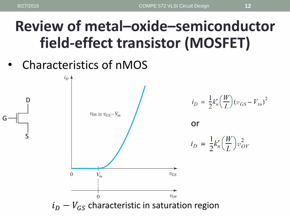
8/27/2015 COMPE 572 VLSI Circuit Design 12
Review of metal–oxide–semiconductor field-effect transistor (MOSFET)
• Characteristics of nMOS
𝑖𝐷 − 𝑉𝐺𝑆 characteristic in saturation region
or G
S
D

8/27/2015 COMPE 572 VLSI Circuit Design 13
Review of metal–oxide–semiconductor field-effect transistor (MOSFET)
• Characteristics of pMOS
G
D
S
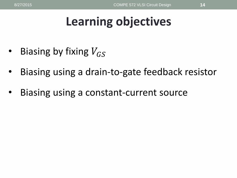
• Biasing by fixing 𝑉𝐺𝑆
• Biasing using a drain-to-gate feedback resistor
• Biasing using a constant-current source
8/27/2015 COMPE 572 VLSI Circuit Design 14
Learning objectives

8/27/2015 COMPE 572 VLSI Circuit Design 15
MOSFET Bias Design
• MOSFET characteristics
G
S
D
We need to consider all the 3 regions (cutoff, triode, saturation) for designing digital circuits, today we will focus on the saturation region
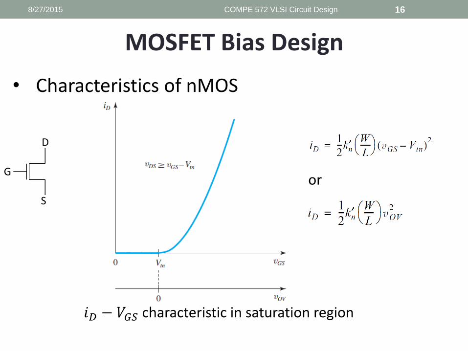
8/27/2015 COMPE 572 VLSI Circuit Design 16
• Characteristics of nMOS
𝑖𝐷 − 𝑉𝐺𝑆 characteristic in saturation region
or G
S
D
MOSFET Bias Design

8/27/2015 COMPE 572 VLSI Circuit Design 17
• Why we need to bias transistors
MOSFET Bias Design
Bias: State of the transistor when there is no signal (current and voltages in all elements) Bias is constant in time (may vary extremely slowly
compared to signal) Purpose of the bias is to ensure that MOS is in saturation
at all times.

8/27/2015 COMPE 572 VLSI Circuit Design 18
MOSFET Bias Design
• Biasing by fixing 𝑉𝐺𝑆
G
S
D
Fixed voltage value
GND
Subject to change
Fixed voltage value
8/27/2015 COMPE 572 VLSI Circuit Design 19
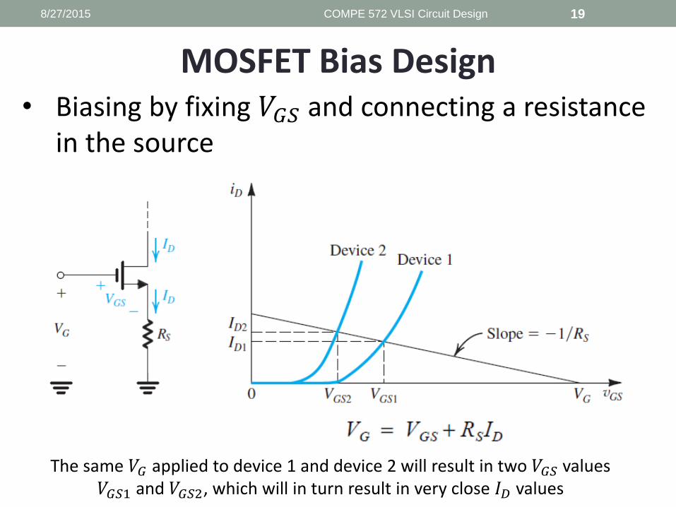
MOSFET Bias Design • Biasing by fixing 𝑉𝐺𝑆 and connecting a resistance
in the source
The same 𝑉𝐺 applied to device 1 and device 2 will result in two 𝑉𝐺𝑆 values 𝑉𝐺𝑆1 and 𝑉𝐺𝑆2, which will in turn result in very close 𝐼𝐷 values

8/27/2015 COMPE 572 VLSI Circuit Design 20
MOSFET Bias Design • Biasing by fixing 𝑉𝐺𝑆 and connecting a resistance
in the source: practical implementations
8/27/2015 COMPE 572 VLSI Circuit Design 21
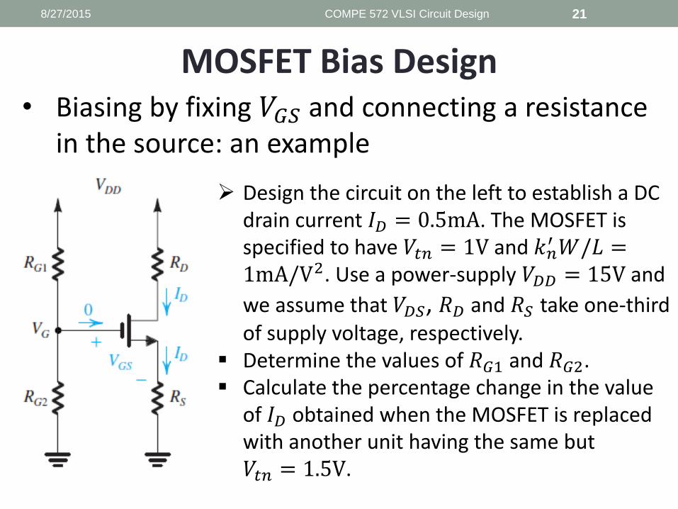
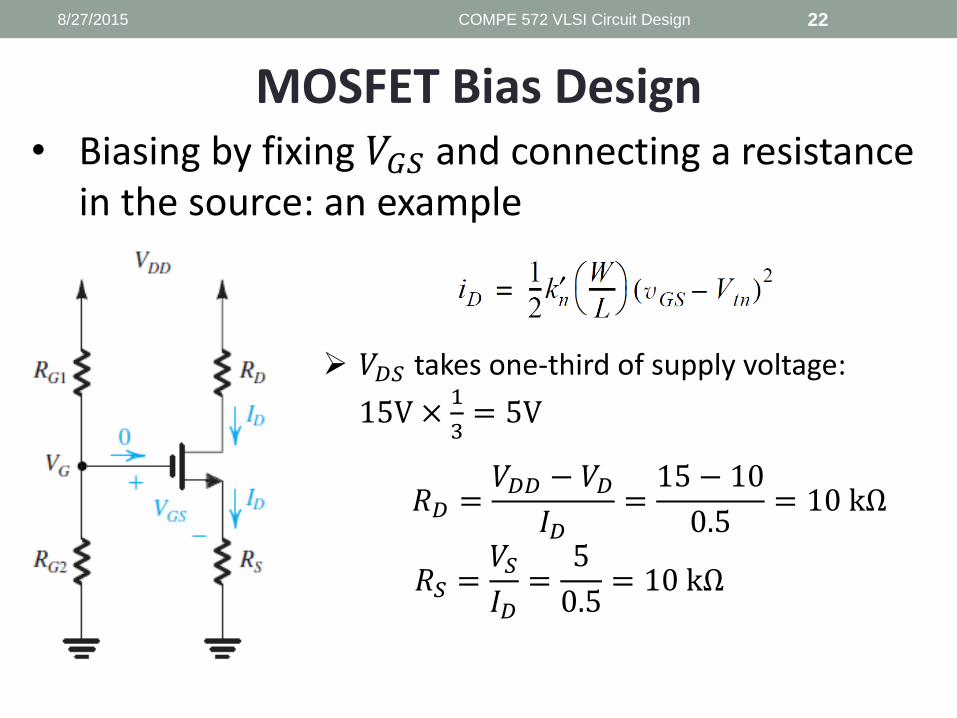
MOSFET Bias Design • Biasing by fixing 𝑉𝐺𝑆 and connecting a resistance
in the source: an example
Design the circuit on the left to establish a DC drain current 𝐼𝐷 = 0.5mA. The MOSFET is specified to have 𝑉𝑡𝑛 = 1V and 𝑘𝑛
′ 𝑊/𝐿 =1mA/V2. Use a power-supply 𝑉𝐷𝐷 = 15V and
we assume that 𝑉𝐷𝑆, 𝑅𝐷 and 𝑅𝑆 take one-third of supply voltage, respectively.
Determine the values of 𝑅𝐺1 and 𝑅𝐺2. Calculate the percentage change in the value
of 𝐼𝐷 obtained when the MOSFET is replaced with another unit having the same but 𝑉𝑡𝑛 = 1.5V.
8/27/2015 COMPE 572 VLSI Circuit Design 22
MOSFET Bias Design • Biasing by fixing 𝑉𝐺𝑆 and connecting a resistance
in the source: an example
𝑉𝐷𝑆 takes one-third of supply voltage:
15V ×1
3= 5V
𝑅𝐷 =𝑉𝐷𝐷 − 𝑉𝐷
𝐼𝐷=
15 − 10
0.5= 10 kΩ
𝑅𝑆 =𝑉𝑆
𝐼𝐷=
5
0.5= 10 kΩ

8/27/2015 COMPE 572 VLSI Circuit Design 23
MOSFET Bias Design • Biasing by fixing 𝑉𝐺𝑆 and connecting a resistance
in the source: an example
Determine 𝑉𝐺𝑆
𝐼𝐷 =1
2𝑘𝑛′(𝑊/𝐿)(𝑣𝐺𝑆 − 𝑉𝑡𝑛)2
⇒ 𝑣𝐺𝑆 = 2 V
0.5 =1
2× 1 × (𝑣𝐺𝑆 − 1)2
⇒ 𝑣𝐺 = 𝑉𝑠 + 𝑉𝐺𝑆 = 5 + 2 = 7 V
We can set 𝑅𝐺1 = 8 MΩ and 𝑅𝐺2 = 7 MΩ

8/27/2015 COMPE 572 VLSI Circuit Design 24
MOSFET Bias Design • Biasing by fixing 𝑉𝐺𝑆 and connecting a resistance
in the source: an example
If 𝑉𝑡𝑛 = 1.5V this time
𝐼𝐷 =1
2× 1 × (𝑣𝐺𝑆 − 1.5)2 … (1)
𝑣𝐺 = 𝑉𝑠 + 𝑉𝐺𝑆 = 𝐼𝐷𝑅𝑆 + 𝑉𝐺𝑆
7 = 104𝐼𝐷 + 𝑉𝐺𝑆 … (2)
⇒ 𝐼𝐷 = 0.455mA
Percentage change is |0.455−0.5|
0.5= 9%
Combining (1) and (2), we have
• Biasing by fixing 𝑉𝐺𝑆
• Biasing using a drain-to-gate feedback resistor
• Biasing using a constant-current source
8/27/2015 COMPE 572 VLSI Circuit Design 25
Learning objectives

8/27/2015 COMPE 572 VLSI Circuit Design 26
MOSFET Bias Design • Biasing using a drain-to-gate feedback resistor
𝑉𝐷𝐷
Slope = −1/𝑅𝐷

• Biasing by fixing 𝑉𝐺𝑆
• Biasing using a drain-to-gate feedback resistor
• Biasing using a constant-current source
8/27/2015 COMPE 572 VLSI Circuit Design 27
Learning objectives

8/27/2015 COMPE 572 VLSI Circuit Design 28
MOSFET Bias Design • Biasing using a constant-current source
General scheme
Large input resistance value
Constant current source

8/27/2015 COMPE 572 VLSI Circuit Design 29
MOSFET Bias Design • Biasing using a constant-current source
Implementation of the constant-current source 𝐼 using a current mirror

8/27/2015 COMPE 572 VLSI Circuit Design 30
MOSFET Bias Design • Biasing using a constant-current source
Analysis of current mirror
⇒

8/27/2015 COMPE 572 VLSI Circuit Design 31
MOSFET Bias Design • Biasing using a constant-current source
Analysis of current mirror
The output current value 𝐼 (or 𝐼𝐷2) can be easily controlled by setting the W and L in the transistor 𝑄2
8/27/2015 COMPE 572 VLSI Circuit Design 32
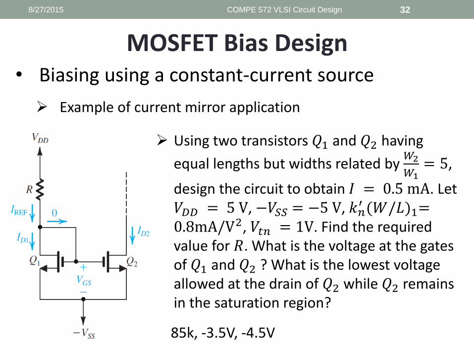
MOSFET Bias Design • Biasing using a constant-current source
Example of current mirror application
Using two transistors 𝑄1 and 𝑄2 having
equal lengths but widths related by 𝑊2
𝑊1= 5,
design the circuit to obtain 𝐼 = 0.5 mA. Let 𝑉𝐷𝐷 = 5 V, −𝑉𝑆𝑆 = −5 V, 𝑘𝑛
′ (𝑊/𝐿)1=0.8mA/V2, 𝑉𝑡𝑛 = 1V. Find the required value for 𝑅. What is the voltage at the gates of 𝑄1 and 𝑄2 ? What is the lowest voltage allowed at the drain of 𝑄2 while 𝑄2 remains in the saturation region?
85k, -3.5V, -4.5V

8/27/2015 COMPE 572 VLSI Circuit Design 33
Summary
• Biasing by fixing 𝑉𝐺𝑆
• Biasing using a drain-to-gate feedback resistor
• Biasing using a constant-current source