
Lecture overview - Computer Science and Engineeringcs2121/LectureNotes/week11_notes_2010.pdf ·...
38
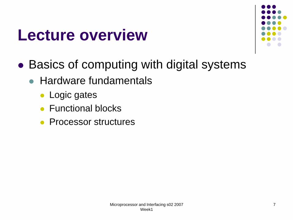
Microprocessor and Interfacing s02 2007 Week1 7 Lecture overview z Basics of computing with digital systems z Hardware fundamentals z Logic gates z Functional blocks z Processor structures
Transcript of Lecture overview - Computer Science and Engineeringcs2121/LectureNotes/week11_notes_2010.pdf ·...
Microprocessor and Interfacing s02 2007 Week1
7
Lecture overview
Basics of computing with digital systemsHardware fundamentals
Logic gatesFunctional blocksProcessor structures
Microprocessor and Interfacing s02 2007 Week1
8
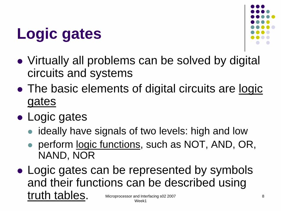
Logic gatesVirtually all problems can be solved by digital circuits and systemsThe basic elements of digital circuits are logic gatesLogic gates
ideally have signals of two levels: high and lowperform logic functions, such as NOT, AND, OR, NAND, NOR
Logic gates can be represented by symbols and their functions can be described using truth tables.

Microprocessor and Interfacing s02 2007 Week1
9
NOT, AND & OR gates
NOT
AND
OR
X Z = X
symbol function
XY
Z = X•Y
XY Z = X+Y
X Z0 11 0
X Y X•Y0 0 00 1 01 0 01 1 1
X Y X+Y0 0 00 1 11 0 11 1 1
X Zlow highhigh low
X Y X•Ylow low lowlow high lowhigh low lowhigh high high
X Y X+Ylow low lowlow high highhigh low highhigh high high

Microprocessor and Interfacing s02 2007 Week1
10
NAND & NOR gates
NAND
NOR
symbol function
XY
Z = X•YX Y X•Y0 0 10 1 11 0 11 1 0
X Y X+Y0 0 10 1 01 0 01 1 0
XY Z = X+Y

Microprocessor and Interfacing s02 2007 Week1
11
XOR & XNOR gates
XOR
XNOR
symbol function
XY
Z = X⊕Y X Y X⊕Y0 0 00 1 11 0 11 1 0
X Y X⊕Y0 0 10 1 01 0 01 1 1
XY Z = X⊕Y

Microprocessor and Interfacing s02 2007 Week1
12
Functional blocks
With basic logic gates we can build up different functional blocks such as
AddersMultiplexersDecodersLatchesRegistersCounters
Microprocessor and Interfacing s02 2007 Week1
13
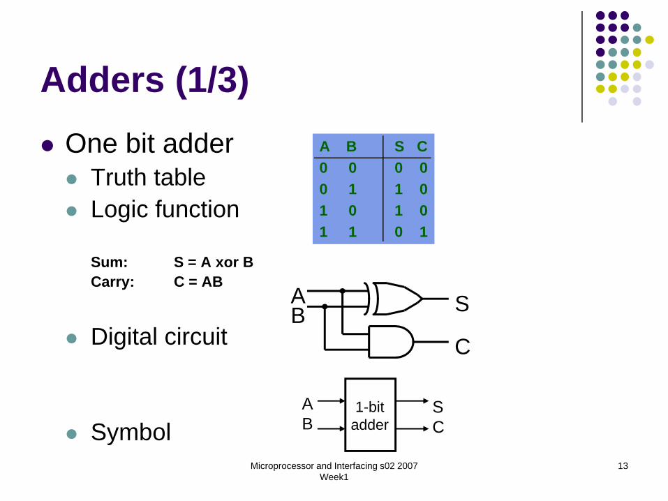
Adders (1/3)One bit adder
Truth tableLogic function
Sum: S = A xor BCarry: C = AB
Digital circuit
Symbol
A B S C0 0 0 00 1 1 01 0 1 01 1 0 1
S
C
AB
1-bitadder
AB
SC

Microprocessor and Interfacing s02 2007 Week1
14
Adders (2/3)
One bit adder with carryCalled Full AdderSymbol
FunctionAdding three 1-bit numbers
Fulladder
ABCin
SCout
A B Cin S Cout0 0 0 0 00 0 1 1 00 1 0 1 00 1 1 0 11 0 0 1 01 0 1 0 11 1 0 0 11 1 1 1 1

Microprocessor and Interfacing s02 2007 Week1
15
Adders (3/3)
n-bit adderSymbol
FunctionAdding two n-bit numbers
The result is n-bit sum and 1-bit carry
n-bitadder
AB
SC
n
n
n

Microprocessor and Interfacing s02 2007 Week1
16
MultiplexerFunction:
A multiplexer selects one input among multiple inputs and passes it to output.
The selection is controlled by control signal Sn-1 ~S0
The symbol:D0
D1
Dm-1
Sn-1 S0
Ym:1 mux
…
OR mux

Microprocessor and Interfacing s02 2007 Week1
17
Example4:1 multiplexer
Function: When S1S0 = 00, Y=D0When S1S0 = 01, Y=D1When S1S0 = 10, Y=D2When S1S0 = 11, Y=D3
D0
D1
D2
D3
S1 S0
Y4:1 mux

Microprocessor and Interfacing s02 2007 Week1
18
MUX example in AVR
Microprocessor and Interfacing s02 2007 Week1
19
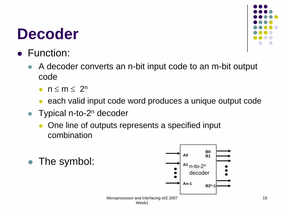
DecoderFunction:
A decoder converts an n-bit input code to an m-bit output code
n ≤ m ≤ 2n
each valid input code word produces a unique output code Typical n-to-2n decoder
One line of outputs represents a specified input combination
The symbol:A0
A1
An-1
n-to-2n
decoder
B0B1
B2n-1
Microprocessor and Interfacing s02 2007 Week1
20
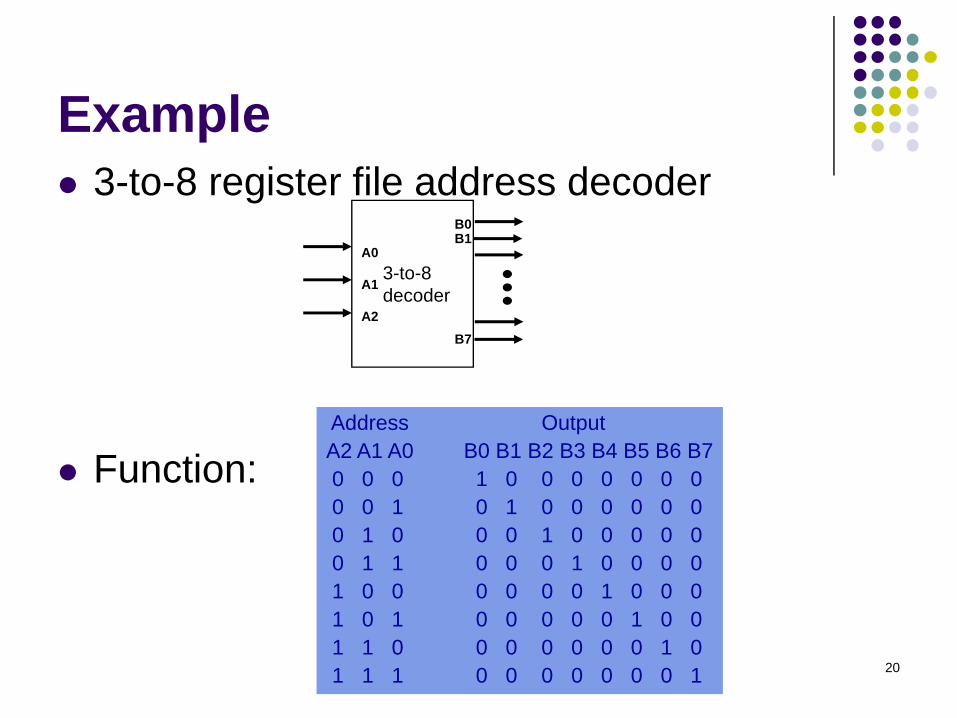
Example3-to-8 register file address decoder
Function: Address OutputA2 A1 A0 B0 B1 B2 B3 B4 B5 B6 B70 0 0 1 0 0 0 0 0 0 00 0 1 0 1 0 0 0 0 0 00 1 0 0 0 1 0 0 0 0 00 1 1 0 0 0 1 0 0 0 01 0 0 0 0 0 0 1 0 0 0 1 0 1 0 0 0 0 0 1 0 0 1 1 0 0 0 0 0 0 0 1 0 1 1 1 0 0 0 0 0 0 0 1
A0
A1
A2
3-to-8decoder
B0B1
B7
Microprocessor and Interfacing s02 2007 Week1
21
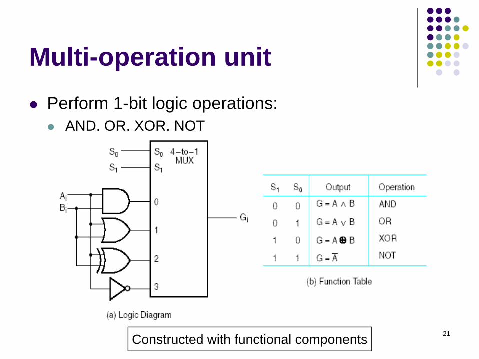
Multi-operation unitPerform 1-bit logic operations:
AND, OR, XOR, NOT
Constructed with functional components

Microprocessor and Interfacing s02 2007 Week1
22
ALU
Perform arithmetic and logic operations such as addition, subtraction, logic AND, Logic OR
Symbol:A, B are operands, S selects one of operations in ALU
A
BALU R
S
OR ALU

Microprocessor and Interfacing s02 2007 Week1
23
Example
Operation selection Operation S2 S1 S0
0 0 0 Addition0 0 1 Subtraction0 1 0 AND0 1 1 OR1 0 0 XOR1 0 1 NOT1 1 0 Increment1 1 1 Transfer

Microprocessor and Interfacing s02 2007 Week1
24
ALU example in AVR

Microprocessor and Interfacing s02 2007 Week1
25
Latches and Flip Flops (1/3)
A latch can store one bit information.Can be constructed in many ways.2-NAND gate latch
R=0, reset the latchS=0, set latchS = R = 1, store the data
R
S Q
Q

Microprocessor and Interfacing s02 2007 Week1
26
Latches and Flip Flops (2/3)Clocked latch uses clock to control the latch operation
When Clk=1,S=1, set the latchS=1, reset the latchS=R=0, store data
When Clk=0,Data is retained
S
R
Q
Q
Clk
Microprocessor and Interfacing s02 2007 Week1
27
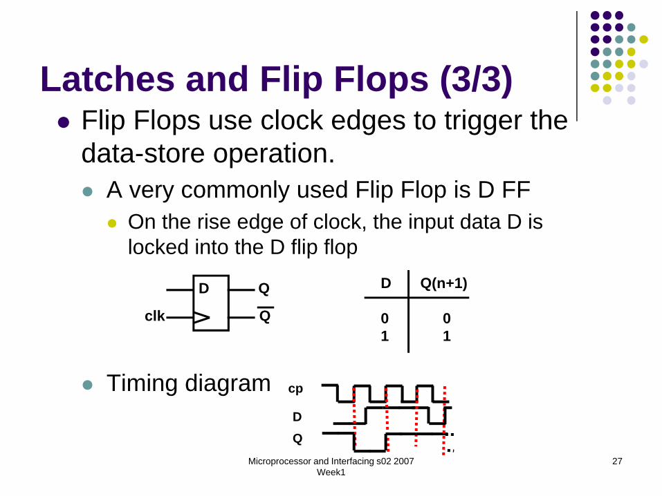
Latches and Flip Flops (3/3)Flip Flops use clock edges to trigger the data-store operation.
A very commonly used Flip Flop is D FFOn the rise edge of clock, the input data D is locked into the D flip flop
Timing diagram
clk
D Q
Q
D Q(n+1)
0 01 1
cp
DQ

Microprocessor and Interfacing s02 2007 Week1
28
Registers (1/3)A register is a collection of latches/FFs
storing a vector of bit valuessymbol
PC
15 8 7 0R(H) R(L)

Microprocessor and Interfacing s02 2007 Week1
29
Registers (2/3)4-bit Parallel In Parallel Out (PIPO) registers.
D Q
CP
I3 Q3
D QI2 Q2
D QI1 Q1
D QI0 Q0
The 4-bit input I3I2I1I0 is “loaded” (copied to the output Q3Q2Q1Q0 of the D FFs) on the rising clock edge, and that output is held until the next clock edge.

Microprocessor and Interfacing s02 2007 Week1
30
Registers (3/3)4-bit Serial In Parallel Out (PISO) registers.
On the clock edge, the output of each flip-flop is passed to the next flip-flop in the chain. The input signal is fed serially (one bit at a time) into the first flip-flop. The flip-flop outputs are available in parallel
Clk
D Q
Q0
D Q
Q1
D Q
Q2
D Q
Q3
Input

Microprocessor and Interfacing s02 2007 Week1
31
Counters (1/2)
A counter increases/decrease its value every clock cycle.

Microprocessor and Interfacing s02 2007 Week1
32
Counters (2/2)
4-bit counterD3 Q3
D2 Q2
D1 Q1
D0 Q0
CLEAR
CP
LOAD
Clock
0
0
0
0
Reset
• with a synchronous load• an asynchronous clear• counts through 0, 1, 2, …, 15, 0

Microprocessor and Interfacing s02 2007 Week1
33
Digital systems
A digital system generally includes two parts:Datapath
Performing a variety of operations on data from different sources
Control unitControlling the selection of the operation and data

Microprocessor and Interfacing s02 2007 Week1
34
CPU
K. Meno, “Logic and Computer Design Fundamentals”

Microprocessor and Interfacing s02 2007 Week1
35
Example of datapath operations
K. Meno, “Logic and Computer Design Fundamentals”

Microprocessor and Interfacing s02 2007 Week1
36
Control unit
Control signals determine the operation of the datapathWhere do the control signals come from?
from control unitControl unit takes the instruction from instruction memory, together with the status values from datapath, to generate the control signals

Microprocessor and Interfacing s02 2007 Week1
37
Some practical designsTri-state buffer
Has three output statesHigh level signal (1) passed from the inputLow level signal (0) passed from the inputHigh impedance (Hi-Z)
Disconnecting the input devices to the output devicesAllows multiple logic gates to drive the same output (e.g, bus)
INEN
OUT
EN IN OUT
0 X Hi-Z1 0 01 1 1
Microprocessor and Interfacing s02 2007 Week1
38
Some practical designs
Open collectorAct like one-way switch
When it is “Open”, no controlling operations

Microprocessor and Interfacing s02 2007 Week1
39
Example
Pullup resistor
Chip 1
Chip 2
MicroINT/
Open collectorinterrupt output that asserts low
Another open collectorinterrupt output that asserts low
Microprocessorinterrupt input that asserts low
Microprocessor and Interfacing s02 2007 Week1
40
For comprehensive coverage of digital systems design, please go to COMP3222
Digital Circuits and Systems Offered S2 each year
Microprocessor and Interfacing s02 2007 Week1
41
Reading material
Appendix B in Computer Organization and Design, The hardware/software interface.

Microprocessor and Interfacing s02 2007 Week1
42
Questions
1. Draw the truth table of the following circuit.
S Co
CiBA
Microprocessor and Interfacing s02 2007 Week1
43
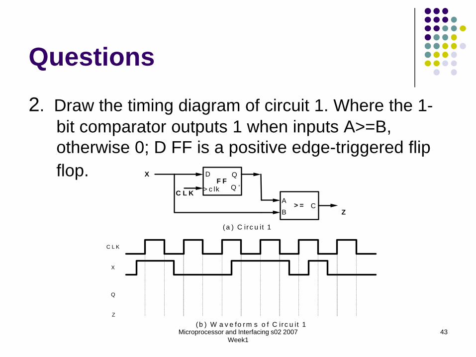
Questions
2. Draw the timing diagram of circuit 1. Where the 1-bit comparator outputs 1 when inputs A>=B, otherwise 0; D FF is a positive edge-triggered flip flop.
F FQ
Q ’> c lk
D
> =AB
C
X
Z
(a ) C irc u it 1
C L K
C L K
X
Q
(b ) W a v e fo rm s o f C irc u it 1Z

Microprocessor and Interfacing s02 2007 Week1
44
Questions
3. Construct a digital circuit with functional blocks such that the circuit can perform the following multiplications: bx0, bx1, bx2, bx4, where b is a positive number and all numbers including the multiplication results can be represented by 8-bits.


![ENSC380 Lecture 28 Objectives: z-TransformUnilateral z-Transform • Analogous to unilateral Laplace transform, the unilateral z-transform is defined as: X(z) = X∞ n=0 x[n]z−n](https://static.fdocuments.net/doc/165x107/61274ac3cd707f40c43ddb9a/ensc380-lecture-28-objectives-z-unilateral-z-transform-a-analogous-to-unilateral.jpg)


