Lecture Notes in Computer Science 3045
15
Transcript of Lecture Notes in Computer Science 3045
Lecture Notes in Computer Science 3045Commenced Publication in 1973Founding and Former Series Editors:Gerhard Goos, Juris Hartmanis, and Jan van Leeuwen
Editorial Board
Takeo KanadeCarnegie Mellon University, Pittsburgh, PA, USA
Josef KittlerUniversity of Surrey, Guildford, UK
Jon M. KleinbergCornell University, Ithaca, NY, USA
Friedemann MatternETH Zurich, Switzerland
John C. MitchellStanford University, CA, USA
Oscar NierstraszUniversity of Bern, Switzerland
C. Pandu RanganIndian Institute of Technology, Madras, India
Bernhard SteffenUniversity of Dortmund, Germany
Madhu SudanMassachusetts Institute of Technology, MA, USA
Demetri TerzopoulosNew York University, NY, USA
Doug TygarUniversity of California, Berkeley, CA, USA
Moshe Y. VardiRice University, Houston, TX, USA
Gerhard WeikumMax-Planck Institute of Computer Science, Saarbruecken, Germany

Antonio Lagana Marina L. GavrilovaVipin Kumar Youngsong MunC.J. Kenneth Tan Osvaldo Gervasi (Eds.)
ComputationalScience and ItsApplications –ICCSA 2004
International ConferenceAssisi, Italy, May 14-17, 2004Proceedings, Part III
1 3
Volume Editors
Antonio LaganaUniversity of Perugia, Department of ChemistryVia Elce di Sotto, 8, 06123 Perugia, ItalyE-mail: [email protected]
Marina L. GavrilovaUniversity of Calgary, Department of Computer Science2500 University Dr. N.W., Calgary, AB, T2N 1N4, CanadaE-mail: [email protected]
Vipin KumarUniversity of Minnesota, Department of Computer Science and Engineering4-192 EE/CSci Building, 200 Union Street SE, Minneapolis, MN 55455, USAE-mail: [email protected]
Youngsong MunSoongSil University, School of Computing, Computer Communication Laboratory1-1 Sang-do 5 Dong, Dong-jak Ku, Seoul 156-743, KoreaE-mail: [email protected]
C.J. Kenneth TanQueen’s University Belfast, Heuchera Technologies Ltd.Lanyon North, University Road, Belfast, Northern Ireland, BT7 1NN, UKE-mail: [email protected]
Osvaldo GervasiUniversity of Perugia, Department of Mathematics and Computer ScienceVia Vanvitelli, 1, 06123 Perugia, ItalyE-mail: [email protected]
Library of Congress Control Number: 2004105531
CR Subject Classification (1998): D, F, G, H, I, J, C.2-3
ISSN 0302-9743ISBN 3-540-22057-7 Springer-Verlag Berlin Heidelberg New York
This work is subject to copyright. All rights are reserved, whether the whole or part of the material isconcerned, specifically the rights of translation, reprinting, re-use of illustrations, recitation, broadcasting,reproduction on microfilms or in any other way, and storage in data banks. Duplication of this publicationor parts thereof is permitted only under the provisions of the German Copyright Law of September 9, 1965,in its current version, and permission for use must always be obtained from Springer-Verlag. Violations areliable to prosecution under the German Copyright Law.
Springer-Verlag is a part of Springer Science+Business Media
springeronline.com
c© Springer-Verlag Berlin Heidelberg 2004Printed in Germany
Typesetting: Camera-ready by author, data conversion by PTP-Berlin, Protago-TeX-Production GmbHPrinted on acid-free paper SPIN: 11010111 06/3142 5 4 3 2 1 0
A. Laganà et al. (Eds.): ICCSA 2004, LNCS 3045, pp. 817–826, 2004. © Springer-Verlag Berlin Heidelberg 2004
Resonant Tunneling Heterostructure Devices – Dependencies on Thickness and Number of Quantum
Wells
Nenad Radulovic, Morten Willatzen, and Roderick V.N. Melnik
Mads Clausen Institute for Product Innovation, University of Southern Denmark, DK-6400 Sonderborg, Denmark
{radulle,willatzen,rmelnik}@mci.sdu.dk
Abstract. We present numerical results for GaAs/AlGaAs double-barrier resonant tunneling heterostructure devices. A particular emphasis is given to the influence of quantum well thickness and number of quantum well layers on current-voltage characteristic and carrier density profile. In the paper, we discuss results obtained for spatial dependencies of carrier densities, the peak and the valley current density, and corresponding potentials in N-shaped current-voltage characteristics for various resonant tunneling heterostructures. Results are based on the transient quantum drift-diffusion model. They are obtained by solving a coupled system of partial differential equations directly and, in contrast to previous analysis, no decoupling algorithms, procedures, or methods are used.
1 Introduction
Semiconductor devices that rely on quantum tunneling through potential barriers are playing an increasingly important role in advanced microelectronic applications, including multiple-state logic, memory devices, and high-frequency oscillators [1,2,3]. The local charge accumulation in quantum wells and nonlinear processes of charge transport across the barriers have been found to provide a number of mechanisms for Negative Differential Resistance/Conductance (NDR/C), bistability of the current at a given voltage, and nonlinear dynamics [4]. The N-shape of Current-Voltage Characteristics (IVC) may be adopted for realizing various logic functions.
By controlled layer-by-layer epitaxial growth of heterostructures in combination with lateral patterning, intricate artificial nanostructures with arbitrary shapes of barriers and wells can be designed and fabricated. Such bandstructure engineering can produce novel semiconductor devices with desired transport and optical properties. The aim of the current research activity in the field is not only to understand the complex and sometimes chaotic spatio-temporal dynamics of charge carriers in such structures, but also to make efficient use of those nonlinear transport properties in specific switching and oscillating electronic devices [4].
Physical device models are based on the physics of carrier transport, and can provide a great insight into the detailed operation of the device. In what follows, particular emphasis is placed upon low-dimensional GaAs/AlGaAs structures and the

818 N. Radulovic, M. Willatzen, and R.V.N. Melnik
nonlinear feedback between the space charges and the transport processes inherent in such structures. In Sect. 2, we present the physical model, as well as time and space discretization. Geometry and relevant parameters of the devices are mainly given in Sect. 3. A short description of numerical simulation is given in Sect. 4. Obtained results are presented and discussed in Sect. 5.
2 Theory and the Model
2.1 Origin and Validity of the Model
In the present paper, we employ the Transient Quantum Drift-Diffusion Model (TQDDM). It is a first-moment version of the isothermal Transient Quantum Hydrodynamic Model (TQHDM), where the velocity convection term is neglected [5]. The origin of the model is due to Ancona et al. [5,6]. The equation of state for the electron gas is generalized and density-gradient dependencies are included, which allow to account for quantum effects [5,6].
The TQDDM is limited to “high” temperatures (T0 77 K) and “low” electron densities (n 3·1019 electrons/cm3), conditions often satisfied in semiconductor structure applications of most interest [7]. The density-gradient expansion is only valid if the coefficient , related to the quantum-correction term, is very small, << 1 [7]. Thus, the lowest-order density-gradient theory gives the best results when the characteristic length is large (L > 10 nm), and the effective mass close to its free-electron value [7].
2.2 The Transient Quantum Drift-Diffusion Model
A detailed derivation of the TQDDM is given by Pinnau et al. [8,9]. Basically, diffusion scaling is introduced in the TQHDM and the TQDDM is derived from a zero relaxation time limit.
The scaled TQDDM equations in 1D, stated on a bounded domain ∈R, read [9]
( )xxt nFn = , (1a)
( ) ( ) FVnnn
xx =++− log12ε ,
(1b)
CnVxx −=− 2λ , (1c)
where the dependent variables are: the electron density n, the quantum quasi-Fermi level F, and the electrostatic potential V. The time-independent doping profile C represents the distribution of charged background ions. The scaled Planck constant , the scaled Debye length , and the scaled relaxation time 0 (used in the numerical time discretization) are defined as
Resonant Tunneling Heterostructure Devices 819
20
*
22
6 LTkm Be
=ε , 2202
LCq
Tk
m
Bsελ = , 2*
202
0 Lm
Tk
e
B ττ = ,
where physical constants are: the reduced Planck constant , the Boltzmann constant kB, and the elementary charge q. Physical parameters are: the effective electron mass me
*, the device operating temperature T0, the permittivity s, and the relaxation time , which depend on the material and the operating conditions of the device. The maximum absolute value of the doping profile C is denoted as Cm, and L is the characteristic (device) length.
The first term on the LHS of eq. (1b) is so-called quantum Bohm potential. The scaled current density, according to eq. (1a), is given by the following expression:
xnFJ −= . (2)
Now, it is possible to introduce an external potential, modeling discontinuities in the conduction band, which occur in the resonant tunneling structures, and other semiconductor heterostructure devices [10]. For that reason, one must replace, in (1b), the potential V by V + B [10], where B is a step function representing the nonnegative quantum well potential. The maximum value Bm, of the step-function B, depends on the content of Al in the ternary alloy composition. It is assumed that Bm = 0.4 eV, which corresponds to 65% Al in AlGaAs at 300 K [2].
In order to get a well-posed problem, the system of eqs. (1) has to be supplemented with appropriate boundary and initial conditions.
The electron density is assumed to fulfill local charge neutrality at the Ohmic contacts. Further, it is natural to assume that there is no normal component of the total current (including the quantum current) along the insulating part of the boundary. Finally, we require that no quantum effects occur at the contacts. These boundary conditions are physically motivated and commonly employed in quantum semiconductor modeling [10]. The numerical investigations in [11] underline the reasonability of this choice.
The boundaries are assumed to be at grid points 0 and M (where M + 1 is the total number of grid points), e.g., at positions x = 0 and x = L, or in scaled coordinates, x = 0 and x = 1, respectively. The corresponding boundary conditions are given below:
00, Ck =ρ , 00, =kF , 00, =kV , (3)
MMk C=,ρ , UF Mk =, , UV Mk =, , (4)
where a new variable n=ρ has been introduced, and U is an applied voltage.
The initial conditions for , F and V are required to start numerical simulation in equilibrium case (U = 0 V). It is natural to set the initial values for F and V to zero, while one has the full freedom to choose/guess the initial value for .

820 N. Radulovic, M. Willatzen, and R.V.N. Melnik
2.3 Discretization in Time and Space
One of the main requirements for the time-discretization is that the scheme should be stable [12,13]. Further, there is no need for higher-order schemes, since the overall discretization error will be dominated by the one introduced through the space-discretization [14,15]. Thus, schemes with first-order accuracy in the time step are sufficient. Moreover, in most of the numerical simulations for the classical Drift-Diffusion Model (DDM), schemes based on backward time differences are employed [12,14]. Since the TQDDM is an O( 2) correction of DDM, it is reasonable to assume this to be true [9]. The most prominent scheme fulfilling the above requirements is the implicit backward Euler method [14,15]. Afterwards, a convenient realizable discrete scheme is derived in two steps: a uniform spatial grid ( x = L/M) is introduced, and the finite difference method is used [13,14,15].
3 Geometry and Relevant Parameters
A Quantum Well (QW) is a synthetic heterostructure containing a very thin layer (thickness of a few nanometers) of one semiconductor sandwiched between two (thin) layers of another semiconductor with a larger bandgap [3]. A superlattice is another important nanostructure, which arises if several alternating layers of two materials with different bandgaps are grown one by one. The potential profile of quantum wells and barriers, which show periodicity, is intimately connected with the charge transport properties of the nanostructures [4].
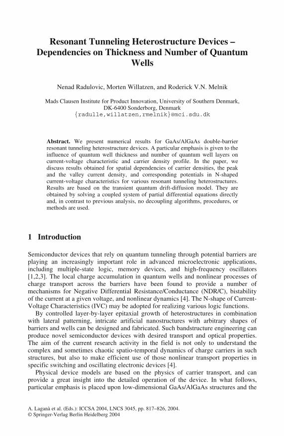
In the present paper, the basic Double Barrier Resonant Tunneling Diode (DBRTD) consists of a quantum well GaAs layer sandwiched between two AlGaAs layers, each 5 nm thick. This resonant structure is itself sandwiched between two spacer GaAs layers of 5 nm thicknesses and supplemented with two contact GaAs regions, each 25 nm thick. The basic n+-n-n+ DBRTD in 2D is shown in Fig. 1. A superlattice has a similar structure with more than one barrier-QW-barrier alternating layers sandwiched between the space layers and supported with two contact regions.
The contact regions are highly doped (n+ type) with Cm = 1024 m-3, while the channel is moderately doped (n type) with Cm = 1021 m-3. The distribution of charged background ions is described by the doping profile C, which is time independent. Such a device exhibits NDR/C due to electron tunneling through the potential barriers. A typical stationary N-shape IVC is well known from the literature.
The domain in 1D case is the interval = [0,L], L > 0 being the device length. The device length is a sum of all layers/regions of the heterostructure. The relaxation time is fixed at = 10-12 s [10]. It is assumed that the devices are operating at liquid-nitrogen temperature, T0 = 77 K. The effective electron mass is chosen to be me
* = 0.067·m0, where m0 is electron rest mass. The permittivity of GaAs/AlGaAs is chosen as s = 13.1· 0, where 0 is permittivity in vacuum. It is also assumed that we operate close to the thermal equilibrium.

Resonant Tunneling Heterostructure Devices 821
GaAs 25 nm (n+)
GaAs5 nm (n)
AlGaAs 5 nm (n)
GaAs5 nm (n)
AlGaAs 5 nm (n)
GaAs5 nm (n)
GaAs 25 nm (n+)
L = 75 nm
Ohmic contact
Ohmic contact
Qua
ntum
Wel
l
Spa
cer La
yer
Spa
cer L a
yer
Bar
rier
Bar
rier
Con
tact
Reg
ion
Con
tact
Re g
ion
Channel
Fig. 1. Basic double barrier resonant tunneling semiconductor structure
4 Numerical Simulation
The numerical simulation is implemented in the Matlab. The system of discretized equations is solved in fully coupled manner for the first time, i.e., in the present work no decoupling algorithms, procedures, or methods are used.
To solve the nonlinear discrete system of equations, which follows from (1), the Newton Iteration Procedure (NIP) is employed [16], where the previous time step is used as initial guess. The following termination criterion is used to stop NIP:
( ) 60,,, 10max −≤− τold
lknew
lklk uu , (5)
where u denotes one of the variables , F and V. The indexes k and l correspond to the time and the space discretization, respectively. Convergence is assumed when the residuals are smaller than a set tolerance.
The scaled time step is changed during the time evolution. Initially, it is set to 10-6 and afterwards increased. The algorithm for the time step is based on two criterions: to speed up the time evolution and to ensure the convergence. The maximum number of required steps in the NIP is less than or equal to 5. Stationary solutions are reached after approximately 150 time steps, depending upon the semiconductor heterostruc-ture under consideration. As a test example for the steady state, the total time is fixed to T = 100 and the same results are obtained.
A uniform grid is used for space discretization. The resolution is set to 4 ppnm (points per nm). It gives us M = 300 for the basic case of a 75 nm DBRTD. We have checked the convergence of calculated variables ( , F, and V) by increasing the resolution (decreasing the grid size) and obtained a relative error less than 1% when 4 ppnm is used.
822 N. Radulovic, M. Willatzen, and R.V.N. Melnik
The obtained results for electron density n, quantum quasi-Fermi level F, and electrostatic potential V are smooth and good agreement in the case of a basic DBRTD heterostructure, also considered in [10], is obtained. Excellent symmetry for equilibrium state (U = 0 V) is present for all semiconductor heterostructures under consideration. The current density in steady state has almost the same value at the Ohmic contacts, as required (relative error is less than 0.5%).
5 Results
Here, we present results for different resonant tunneling heterostructures, obtained with the numerical simulation. In the first case, a DBRTD with one QW is considered corresponding to three different QW sizes (2, 5, and 10 nm), while in the second case, superlattices with 2, 3, and 5 QWs are considered, where each QW is of the same size (5 nm). In all presented cases, width of the barriers and space layers are 5 nm. The length of all DBRTDs is fixed to L = 75 nm (contact regions are 26.5, 25, and 22.5 nm, respectively), while the length of the superlattices is a sum of all layers (contact regions are fixed to 25 nm). The external potential U is always applied on the RHS Ohmic contact, while the LHS contact is grounded. In what follows, we are interested in the spatial dependency of electron densities and afterwards we comment on obtained current-voltage (IV) characteristics.
The results for electron densities for all three DBRTD (QW width 2, 5, and 10 nm), are given in Fig. 2. As a reference, doping profiles are also given. The applied potential is U = 0.2 V, which approximately corresponds to the peak voltage for these three cases. The results are qualitatively different for various thicknesses of the QW. For the case of a 2 nm QW, accumulation of electrons in the QW is evident, however, the resulting density for the “peak”-applied voltage is much less than the doping concentration. For the cases of 5 and 10 nm QW, the accumulation effect of electrons in the QW is indeed very important, and electron densities, for the peak-applied voltage, are significantly larger than doping concentration (two orders of magnitude). This indicates that a minimum thickness of the QW exists, which allows sufficient accumulation of electrons. In addition, the electron density inside the QW shows an increase of spatial asymmetry as the thickness of the QW is increased. A significant electron density reduction is apparent in the barrier regions and the minimums are not the same on both sides of the QW. The densities inside barriers have larger values on the side where the external potential is applied, in contrast to the densities inside the QW. The minimum of the density in the barrier changes significantly with increasing thickness of the QW. In contrast, the peak of the electron density inside QWs of differ ent thicknesses shows “saturation”, i.e., they are almost the same (if the thickness of the QW is large enough, LQW 4-5 nm).
The results for electron densities for the superlattice heterostructures (with 2, 3, and 5 QWs), are given in Fig. 3. As a reference, doping profiles are also given. The applied potentials are U = 0.30 V, 0.35 V, and 0.50 V, which approximately correspond to the peak voltages, respectively. The superlattice heterostructures have different peaks of electron density in different QWs, under the influence of an external potential. In the case of a superlattice with 2 QWs, the charge accumulation in the QW being closer to the side where the external potential is applied, is much smaller, as is the peak. In the case of a superlattice with more than 2 QWs, the peak of

Resonant Tunneling Heterostructure Devices 823
Fig. 2. Densities of electrons n(x) for the DBRTDs with 2, 5, and 10 nm QW; dotted, dashed, and solid curve, respectively; U = 0.2 V; corresponding doping profiles C(x) are represented by bold step-curves with the same line coding as for n(x)
Fig. 3. Densities of electrons n(x) for the superlattices with 2, 3, and 5 QWs; dotted, dashed, and solid curve, respectively; U = 0.30 V, 0.35 V, and 0.50 V, respectively; corresponding doping profiles C(x) are represented by bold step-curves with the same line coding as for n(x)
824 N. Radulovic, M. Willatzen, and R.V.N. Melnik
Fig. 4. The IV characteristics for the DBRTDs with 2, 5, and 10 nm QW; dotted, dashed, and solid curve, respectively
Fig. 5. The IV characteristics for the superlattices with 2, 3, and 5 QWs; dotted, dashed, and solid curve, respectively

Resonant Tunneling Heterostructure Devices 825
the electron density inside QWs changes its magnitude, from the side where the external potential is applied towards the zero-volt (grounded) contact. In general, the QW that is closest to the zero-volt contact has the largest peak of the electron density. In contrast, the minimum of the electron density is always reached in the barrier that is nearby the zero-volt contact.
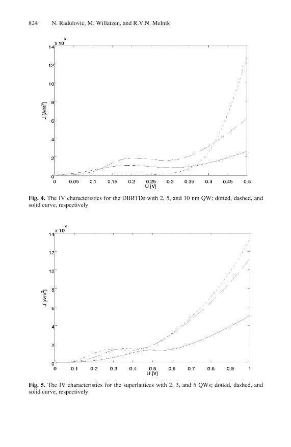
The IV characteristics for the DBRTDs (QW thickness of 2, 5, and 10 nm), are given in Fig. 4. The IV characteristic for the DBRTD with 2 nm QW does not show NDR/C at all. Changing the width of the QW, a significant change in the IV characteristic occurs, i.e., the current density for the same applied voltage is changed. In addition, the peak and the valley current density, and the relative ratio between them, also change significantly. However, the peak and the valley potential will only slightly differ.
The IV characteristics for the superlattice heterostructures with 2, 3, and 5 QWs (corresponding to L = 85, 95, 115 nm, respectively), are given in Fig. 5. It is obvious that an increase of the number of QWs leads to a significant influence on the IV characteristic. At the same time, the peak and the valley potential are also changed, and the current density is reduced. However, the peak and the valley current density will be only slightly changed.
Unfortunately, it is extremely difficult to predict the exact values of the peak and the valley current density in the N-shaped IV characteristics. These values are strongly affected by other mechanisms, such as phonon-assisted tunneling, impurity-assisted tunneling, and scattering. The voltage positions of the current density peaks and valleys are, however, easier to establish, since they are related to energy levels of the subbands.
The computed values of the current density strongly depend on the choice of the intrinsic device parameters. The most important parameters are the effective electron mass and the relaxation time. Thus, the choice of the intrinsic parameters is crucial for the accurate quantitative simulation of the resonant tunneling heterostructures. However, we expect the general tendencies observed here to be correct.
6 Conclusion
The system of fully discretized coupled nonlinear algebraic equations, which follows from (1), is possible to solve avoiding the use of decoupling algorithms, procedures, or methods. The results obtained for different resonant tunneling heterostructures using TQDDM show that the electron density is strongly nonlinear and asymmetric in both, QWs and barriers, under the influence of an external potential. However, in the equilibrium case (U = 0 V), perfect symmetry is present. The IV characteristics of the heterostructure nanodevices are quite different, when varying the thickness and the number of QWs of the device. In particular, changing the thickness of the QW, the peak and the valley current density change significantly, while the peak and the valley potential only slightly differ. In contrast, changing the number of the QWs (keeping the size of the QW constant), the peak and the valley potential change dramatically, while the peak and the valley current are almost unchanged.

826 N. Radulovic, M. Willatzen, and R.V.N. Melnik
References
1. Sze, S.M.: Semiconductor Devices – Physics and Technology. Wiley, New York (1985) 2. Shur, M.: Physics of Semiconductor Devices. Prentice Hall, Englewood Cliffs (1990) 3. Yu, P.Y., Cardona, M.: Fundamentals of Semiconductors – Physics and Materials
Properties. Springer-Verlag, Berlin Heidelberg New York (1996) 4. Scholl, E.: Nonlinear Spatio-Temporal Dynamics and Chaos in Semiconductors.
Cambridge University Press, Cambridge (2001) 5. Ancona, M.G.: Diffusion-Drift Modeling of Strong Inversion Layers. COMPEL, 6 (1987)
11–18 6. Ancona, M.G., Tiersten, H.F.: Macroscopic Physics of the Silicon Inversion Layer. Phys.
Rev. B, Vol. 35, No. 15 (1987) 7959–7965 7. Ancona, M.G., Iafrate, G.J.: Quantum Correction to the Equation of State of an Electron
Gas in a Semiconductor. Phys. Rev. B, Vol. 39, No. 13 (1989) 9536–9540 8. Pinnau, R., Unterreiter, A.: The Stationary Current-Voltage Characteristics of the Quantum
Drift-Diffusion Model. SIAM J. Numer. Anal., Vol. 37, No. 1 (1999) 211–245 9. Pinnau, R.: The Linearized Transient Quantum Drift-diffusion Model – Stability of
Stationary States. ZAMM, 80(5) (2000) 327–344 10. Pinnau, R.: Numerical Approximation of the Transient Quantum Drift-Diffusion Model.
Nonlinear Analysis, Vol. 47 (2001) 5849–5860 11. Pinnau, R.: A Note on Boundary Conditions for Quantum Hydrodynamic Equations. Appl.
Math. Lett., 12 (1999) 77–82 12. Markowich, P.A., Ringhofer, C.A.: Stability of the Linearized Transient Semiconductor
Device Equations. ZAMM, 67(7) (1987) 319–332 13. Markowich, P.A., Ringhofer, C.A., Schmeiser, C.: Semiconductor Equations. Springer-
Verlag, Wien (1991) 14. Mock, M.S.: Analysis of Mathematical Models of Semiconductor Devices. Boole Press,
Dublin (1983) 15. Selberherr, S.: Analysis and Simulation of Semiconductor Devices. Springer-Verlag, Wien
New York (1984) 16. Schatzman, M.: Numerical Analysis – A Mathematical Introduction. Clarendon Press,
Oxford (2002)

XX Table of Contents – Part III
Computational Math, Science, and Technology: A New PedagogicalApproach to Math and Science Education . . . . . . . . . . . . . . . . . . . . . . . . . . . . 807
Osman Yasar
Track on Computer Modeling and Simulation
Resonant Tunneling Heterostructure Devices – Dependencieson Thickness and Number of Quantum Wells . . . . . . . . . . . . . . . . . . . . . . . . . 817
Nenad Radulovic, Morten Willatzen, Roderick V.N. Melnik
Teletraffic Generation of Self-Similar Processes withArbitrary Marginal Distributions for Simulation:Analysis of Hurst Parameters . . . . . . . . . . . . . . . . . . . . . . . . . . . . . . . . . . . . . . . 827
Hae-Duck J. Jeong, Jong-Suk Ruth Lee, Hyoung-Woo Park
Design, Analysis, and Optimization of LCD Backlight Unit UsingRay Tracing Simulation . . . . . . . . . . . . . . . . . . . . . . . . . . . . . . . . . . . . . . . . . . . . 837
Joonsoo Choi, Kwang-Soo Hahn, Heekyung Seo, Seong-Cheol Kim
An Efficient Parameter Estimation Technique fora Solute Transport Equation in Porous Media . . . . . . . . . . . . . . . . . . . . . . . . 847
Jaemin Ahn, Chung-Ki Cho, Sungkwon Kang, YongHoon Kwon
HierGen: A Computer Tool for the Generation ofActivity-on-the-Node Hierarchical Project Networks . . . . . . . . . . . . . . . . . . . 857
Miguel Gutierrez, Alfonso Duran, David Alegre, Francisco Sastron
Macroscopic Treatment to Polymorphic E-mail Based Viruses . . . . . . . . . . 867Cholmin Kim, Soung-uck Lee, Manpyo Hong
Making Discrete Games . . . . . . . . . . . . . . . . . . . . . . . . . . . . . . . . . . . . . . . . . . . . 877Inmaculada Garcıa, Ramon Molla
Speech Driven Facial Animation Using Chinese MandarinPronunciation Rules . . . . . . . . . . . . . . . . . . . . . . . . . . . . . . . . . . . . . . . . . . . . . . . 886
Mingyu You, Jiajun Bu, Chun Chen, Mingli Song
Autonomic Protection System Using Adaptive Security Policy . . . . . . . . . . 896Sihn-hye Park, Wonil Kim, Dong-kyoo Kim
A Novel Method to Support User’s Consent in Usage Control forStable Trust in E-business . . . . . . . . . . . . . . . . . . . . . . . . . . . . . . . . . . . . . . . . . 906
Gunhee Lee, Wonil Kim, Dong-kyoo Kim
Track on Financial and Economical Modeling
No Trade under Rational Expectations in Economy(A Multi-modal Logic Approach) . . . . . . . . . . . . . . . . . . . . . . . . . . . . . . . . . . . 915
Takashi Matsuhisa