Lecture 6: Lithography 2 - dunham.ece.uw.edu · UTD | Fall 2007|EE/MSEN 6322 Semiconductor...
31
<1> Lecture 6: Lithography 2 Lecture 6: Lithography 2 Outline: Mask engineering Resolution enhancements technologies (RET) Model and simulation Next generation lithography (NGL) X-Ray e-beam litho Imprint Litho
Transcript of Lecture 6: Lithography 2 - dunham.ece.uw.edu · UTD | Fall 2007|EE/MSEN 6322 Semiconductor...
<1>Lecture 6: Lithography 2
Lecture 6: Lithography 2Outline:
Mask engineeringResolution enhancements technologies (RET)Model and simulationNext generation lithography (NGL)
X-Raye-beam lithoImprint Litho
UTD | Fall 2007|EE/MSEN 6322 Semiconductor Processing Technology -Dr. W. Hu <2>Lecture 6: Lithography 2
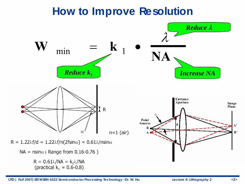
Reduce λ
Increase NAReduce k1
W min = k 1 •λ
NA
How to Improve Resolution
UTD | Fall 2007|EE/MSEN 6322 Semiconductor Processing Technology -Dr. W. Hu <3>Lecture 6: Lithography 2
Aperture Projection Lens
"Captured"Diffracted
Light
"Lost"Diffracted
Light
"Captured"Diffracted
Light
"Lost"Diffracted
Light
Wafer
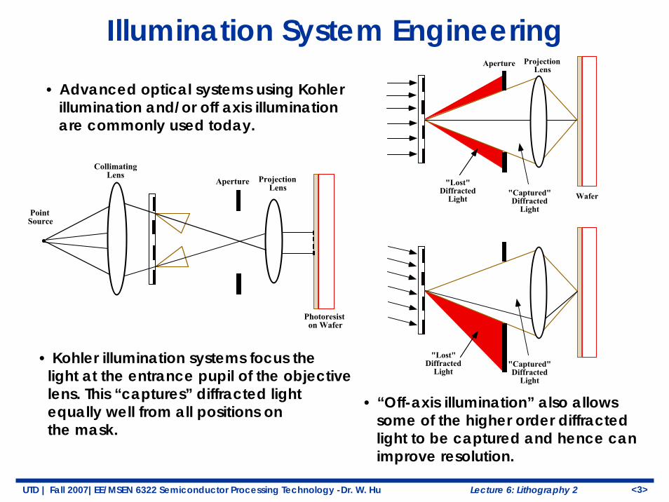
• “Off-axis illumination” also allows some of the higher order diffracted light to be captured and hence can improve resolution.
Aperture
PointSource
Collimating Lens Projection
Lens
Photoresist on Wafer
• Kohler illumination systems focus the light at the entrance pupil of the objective lens. This “captures” diffracted light equally well from all positions on the mask.
• Advanced optical systems using Kohler illumination and/or off axis illuminationare commonly used today.
Illumination System Engineering
UTD | Fall 2007|EE/MSEN 6322 Semiconductor Processing Technology -Dr. W. Hu <4>Lecture 6: Lithography 2
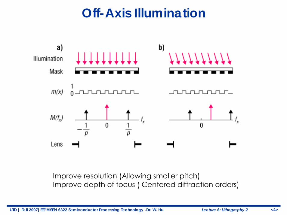
Off-Axis Illumination
Improve resolution (Allowing smaller pitch)Improve depth of focus ( Centered diffraction orders)
UTD | Fall 2007|EE/MSEN 6322 Semiconductor Processing Technology -Dr. W. Hu <5>Lecture 6: Lithography 2
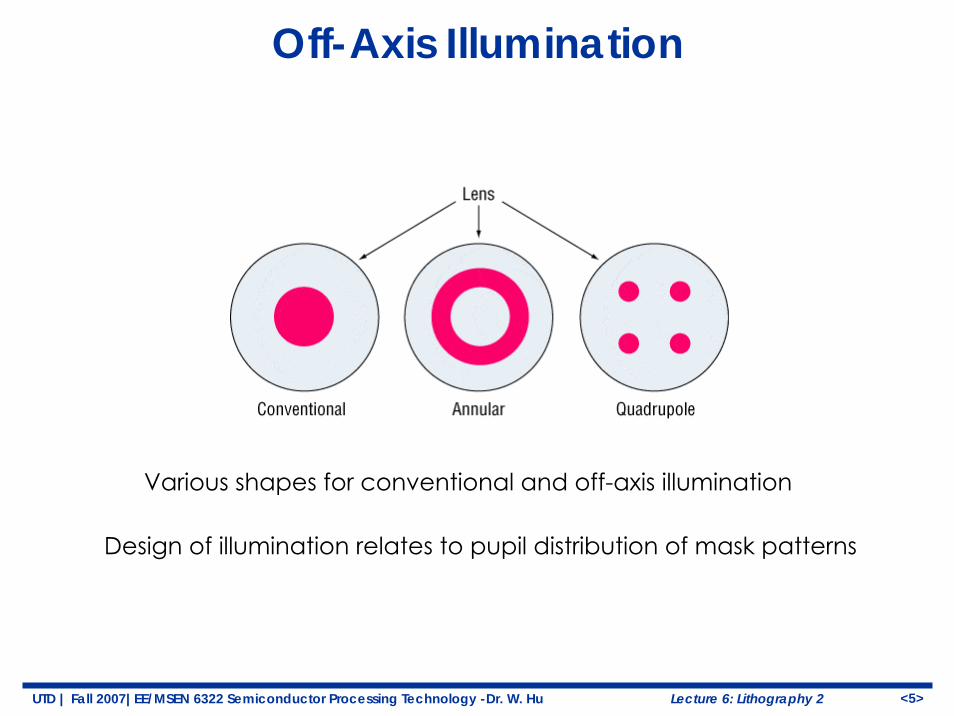
Off-Axis Illumination
Various shapes for conventional and off-axis illumination
Design of illumination relates to pupil distribution of mask patterns
UTD | Fall 2007|EE/MSEN 6322 Semiconductor Processing Technology -Dr. W. Hu <6>Lecture 6: Lithography 2
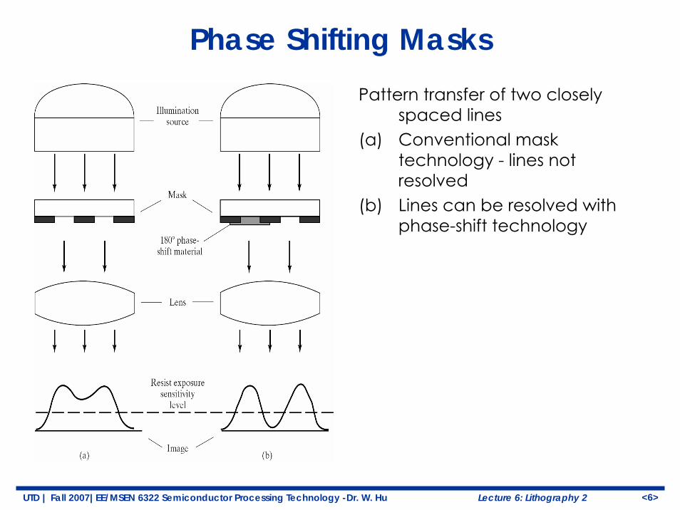
Phase Shifting MasksPattern transfer of two closely
spaced lines(a) Conventional mask
technology - lines not resolved
(b) Lines can be resolved with phase-shift technology

UTD | Fall 2007|EE/MSEN 6322 Semiconductor Processing Technology -Dr. W. Hu <7>Lecture 6: Lithography 2
Bright (+)
Dark (0)
Top Viewof Mask
CrossSection
PhotoresistThreshold
Silicon
Photoresist
Quartz
Chrome
Quartz
Chrome
Wafer
Binary Technology Limits
Source: Photronics.com
UTD | Fall 2007|EE/MSEN 6322 Semiconductor Processing Technology -Dr. W. Hu <8>Lecture 6: Lithography 2
Light WavesOut of Phase
Bright (+)
Dark (0)
Bright (-)
Bright (+)
Dark (0)
Bright (-)
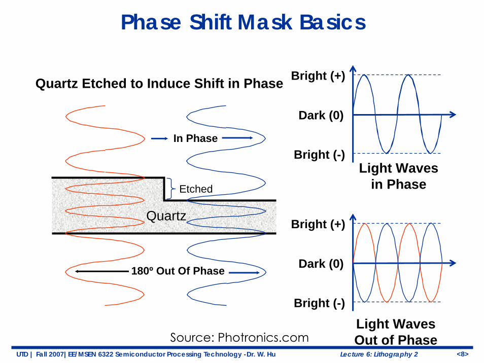
Light Wavesin PhaseEtched
Quartz
180º Out Of Phase
Quartz Etched to Induce Shift in Phase
In Phase
Phase Shift Mask Basics
Source: Photronics.com
UTD | Fall 2007|EE/MSEN 6322 Semiconductor Processing Technology -Dr. W. Hu <9>Lecture 6: Lithography 2
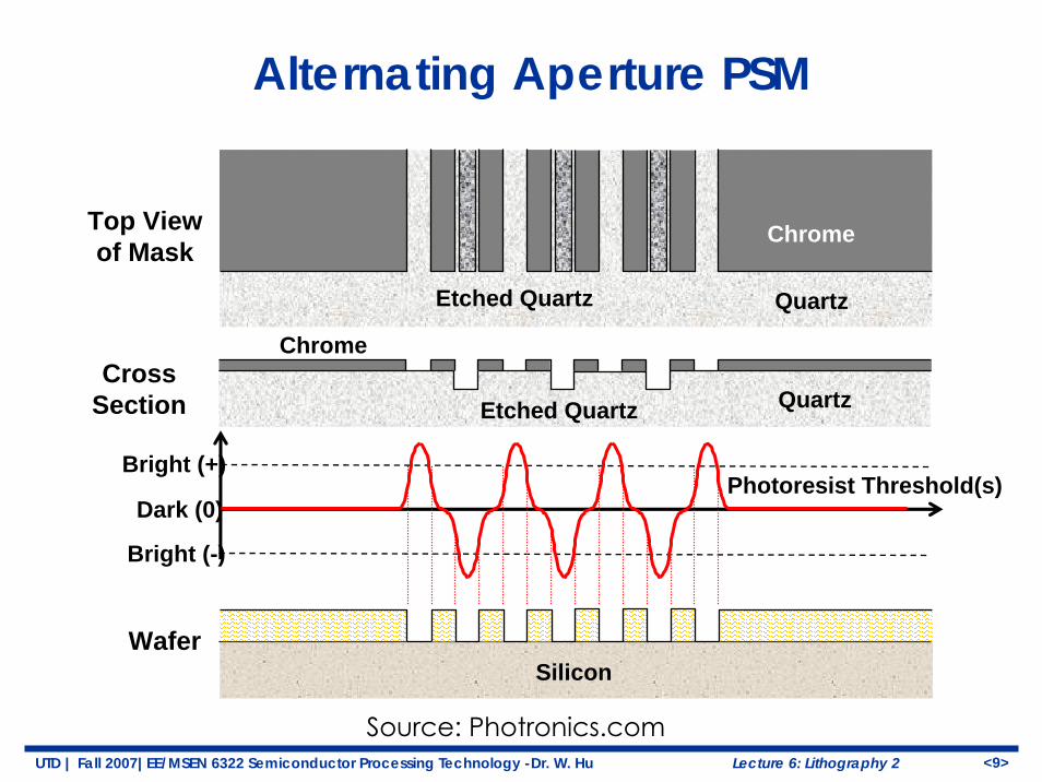
Alternating Aperture PSM
Top Viewof Mask
CrossSection Quartz
Chrome
Quartz
Silicon
Photoresist
Chrome
Wafer
Etched Quartz
Etched Quartz
Photoresist Threshold(s)Bright (+)
Dark (0)
Bright (-)
Source: Photronics.com
UTD | Fall 2007|EE/MSEN 6322 Semiconductor Processing Technology -Dr. W. Hu <10>Lecture 6: Lithography 2
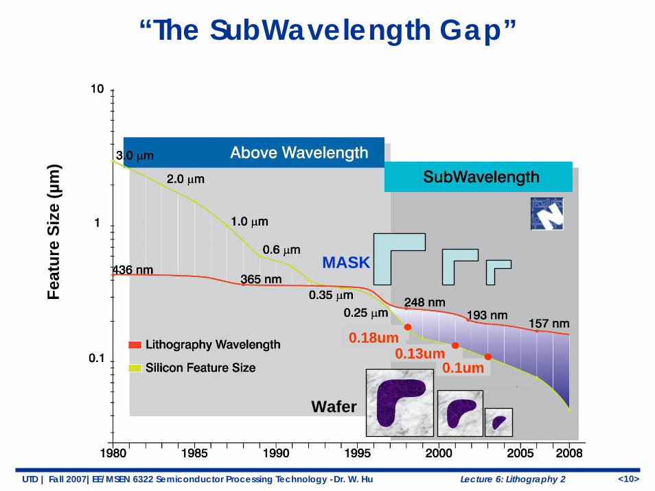
0.18um0.13um
0.1um
Feat
ure
Size
(µm
)“The SubWavelength Gap”
MASK
Wafer

UTD | Fall 2007|EE/MSEN 6322 Semiconductor Processing Technology -Dr. W. Hu <11>Lecture 6: Lithography 2
100nmConventional mask
130nmConventional mask
Mask
180nm Conventional mask
Wafer
Rule-based OPC improves 130nm
Rule-basedOPC
Rule-based OPC
… but not 100 nmModel-based OPC enables
100nm
Model-based OPC
Optical Proximity Correction (OPC)
UTD | Fall 2007|EE/MSEN 6322 Semiconductor Processing Technology -Dr. W. Hu <12>Lecture 6: Lithography 2
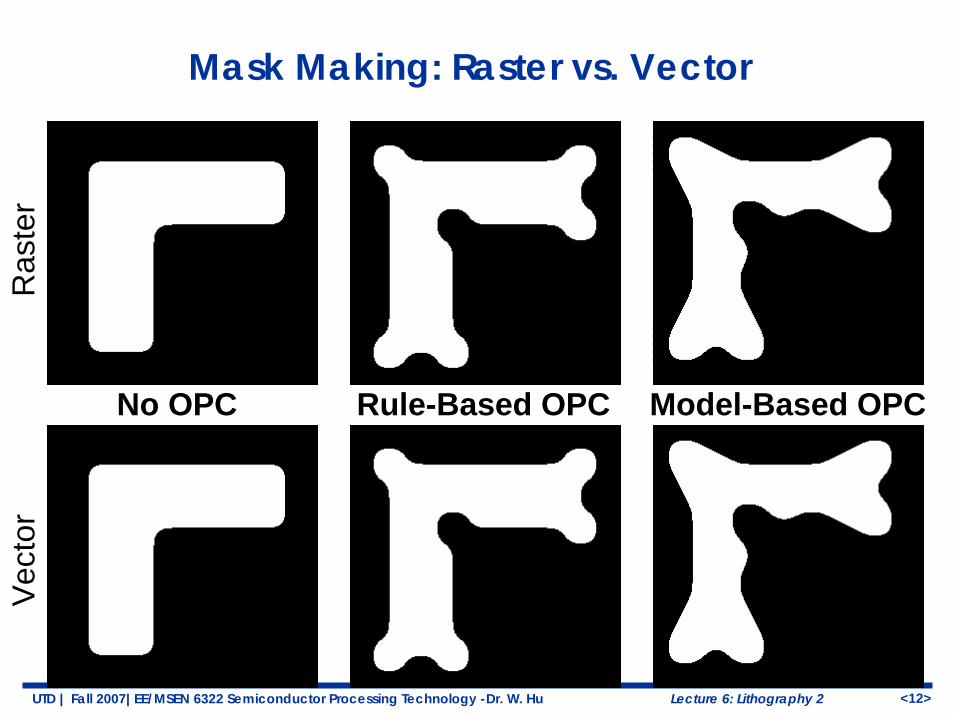
No OPC Rule-Based OPC Model-Based OPC
Ras
ter
Vec
torMask Making: Raster vs. Vector
UTD | Fall 2007|EE/MSEN 6322 Semiconductor Processing Technology -Dr. W. Hu <13>Lecture 6: Lithography 2
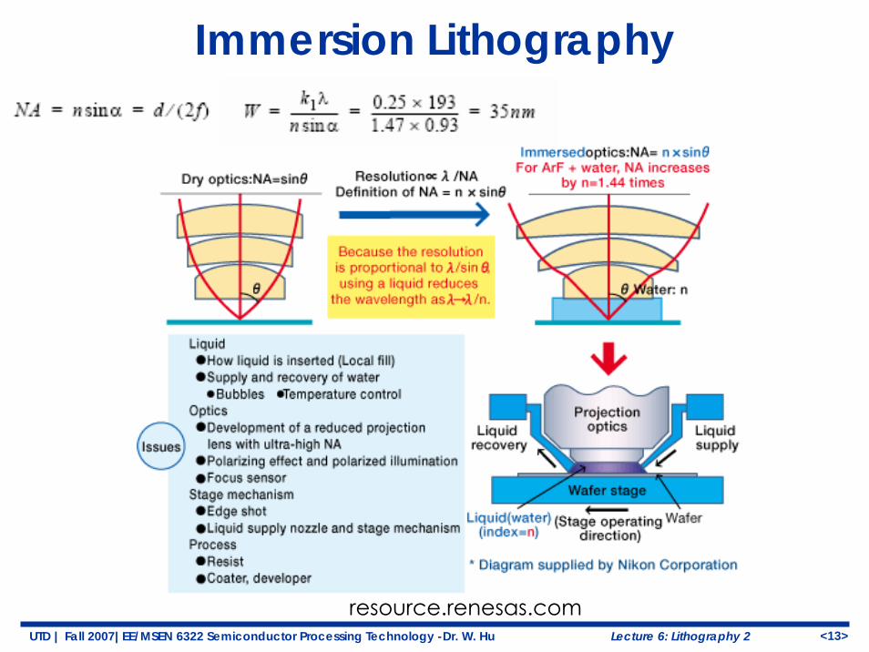
resource.renesas.com
Immersion Lithography
UTD | Fall 2007|EE/MSEN 6322 Semiconductor Processing Technology -Dr. W. Hu <14>Lecture 6: Lithography 2
Microns
Mic
rons 0
1
2
3
-1
-2
-3 0 1 2 3-1-2
-3
Microns0 1 2-1-2
Mic
rons 0
1
2
-1
-2
Mic
rons 0
1
2
-1
-2
Microns0 1 2-1-2
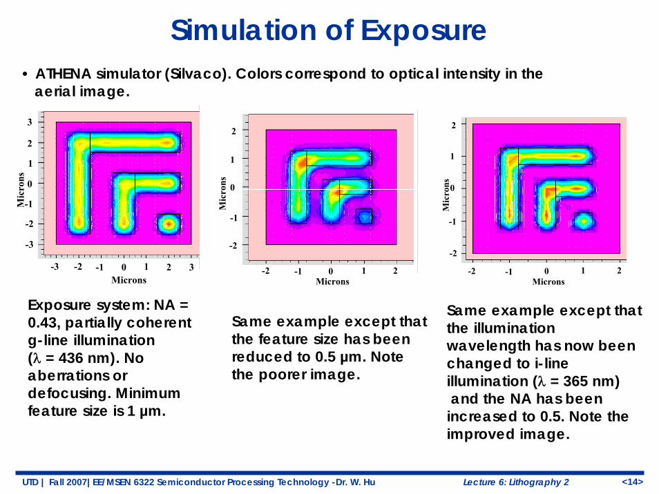
• ATHENA simulator (Silvaco). Colors correspond to optical intensity in the aerial image.
Exposure system: NA = 0.43, partially coherent g-line illumination (λ = 436 nm). No aberrations or defocusing. Minimum feature size is 1 µm.
Same example except that the feature size has been reduced to 0.5 µm. Note the poorer image.
Same example except that the illumination wavelength has now been changed to i-line illumination (λ = 365 nm)and the NA has been
increased to 0.5. Note the improved image.
Simulation of Exposure
UTD | Fall 2007|EE/MSEN 6322 Semiconductor Processing Technology -Dr. W. Hu <15>Lecture 6: Lithography 2
Microns0 0.8 1.6 2.4
Mic
rons
0
0.4
0.8
1.2
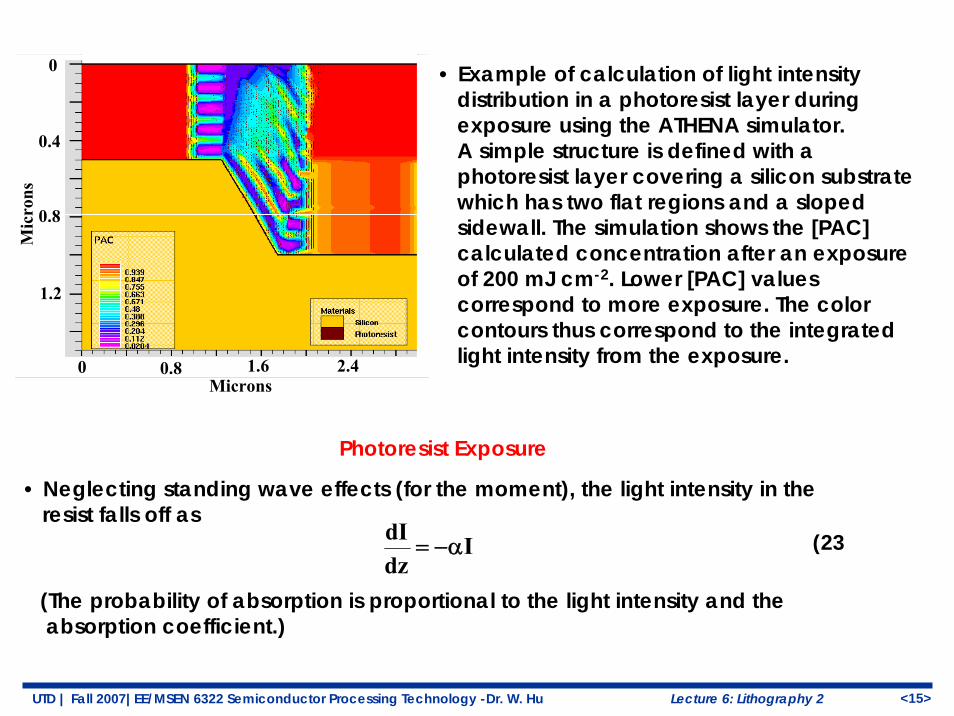
• Example of calculation of light intensity distribution in a photoresist layer during exposure using the ATHENA simulator. A simple structure is defined with a photoresist layer covering a silicon substrate which has two flat regions and a sloped sidewall. The simulation shows the [PAC] calculated concentration after an exposure of 200 mJ cm-2. Lower [PAC] values correspond to more exposure. The color contours thus correspond to the integrated light intensity from the exposure.
Photoresist Exposure
• Neglecting standing wave effects (for the moment), the light intensity in the resist falls off as
dIdz
= −αI (23
(The probability of absorption is proportional to the light intensity and theabsorption coefficient.)
UTD | Fall 2007|EE/MSEN 6322 Semiconductor Processing Technology -Dr. W. Hu <16>Lecture 6: Lithography 2
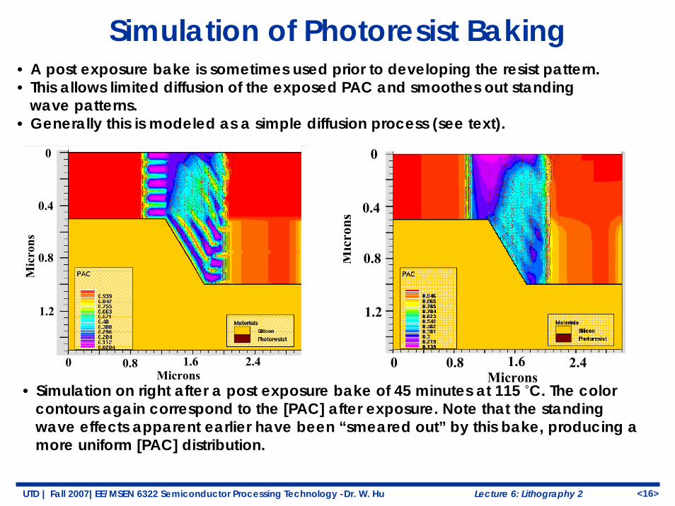
• A post exposure bake is sometimes used prior to developing the resist pattern. • This allows limited diffusion of the exposed PAC and smoothes out standing
wave patterns.• Generally this is modeled as a simple diffusion process (see text).
Microns0.8 1.6 2.40
Mic
rons
0
0.4
0.8
1.2
Microns0 0.8 1.6 2.4
Mic
rons
0
0.4
0.8
1.2
• Simulation on right after a post exposure bake of 45 minutes at 115 ˚C. The color contours again correspond to the [PAC] after exposure. Note that the standing wave effects apparent earlier have been “smeared out” by this bake, producing a more uniform [PAC] distribution.
Simulation of Photoresist Baking
UTD | Fall 2007|EE/MSEN 6322 Semiconductor Processing Technology -Dr. W. Hu <17>Lecture 6: Lithography 2
Mic
rons
0
0.4
0.8
1.2
Microns0.8 1.6 2.40
Microns0.8 1.6 2.40
Mic
rons
0
0.4
0.8
1.2
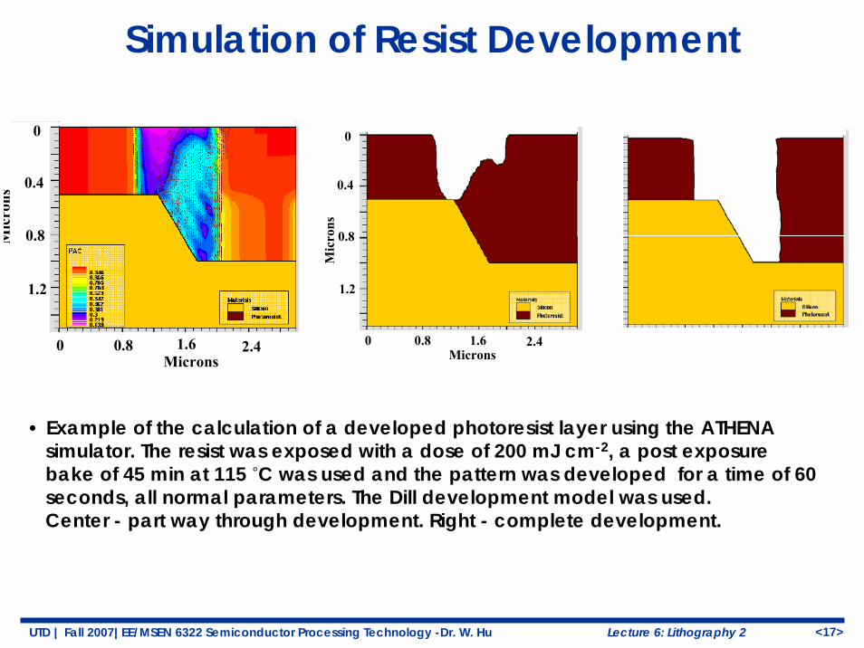
• Example of the calculation of a developed photoresist layer using the ATHENA simulator. The resist was exposed with a dose of 200 mJ cm-2, a post exposurebake of 45 min at 115 ˚C was used and the pattern was developed for a time of 60 seconds, all normal parameters. The Dill development model was used. Center - part way through development. Right - complete development.
Simulation of Resist Development
UTD | Fall 2007|EE/MSEN 6322 Semiconductor Processing Technology -Dr. W. Hu <18>Lecture 6: Lithography 2
Next Generation Lithography• Immersion 193 with RETs
– Double exposures– Multiple Lithography (ML2)– Advanced mask technology…
• Extreme UV (EUV) or Soft X-ray Lithography, 2015-2020.• Nanoimprint, 2008?
– Step and Flash Imprint Lithography (S-FIL)
UTD | Fall 2007|EE/MSEN 6322 Semiconductor Processing Technology -Dr. W. Hu <19>Lecture 6: Lithography 2
X-Ray Lithography• General Characteristics• Energy Sources• Masks• Exposure Systems / Aligners• Resists• Interaction of X-rays with substrate
• Eliminates the diffraction limitations of optical lithography• Issues
– Brightness of sources– Optical components (lens, reflectors, etc.)– Masks– Resists
General Characteristics
UTD | Fall 2007|EE/MSEN 6322 Semiconductor Processing Technology -Dr. W. Hu <20>Lecture 6: Lithography 2
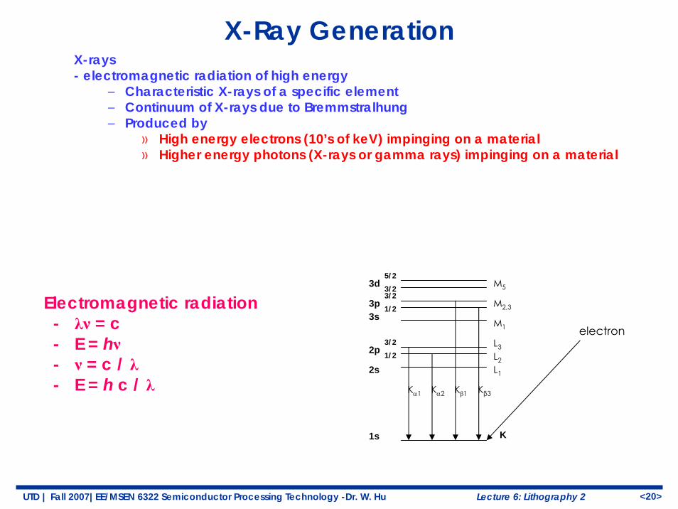
X-Ray GenerationX-rays - electromagnetic radiation of high energy
– Characteristic X-rays of a specific element– Continuum of X-rays due to Bremmstralhung– Produced by
» High energy electrons (10’s of keV) impinging on a material» Higher energy photons (X-rays or gamma rays) impinging on a material
Electromagnetic radiation- λν = c- E = hν- ν = c / λ- E = h c / λ
1s
2s
2p
3s3p
3d
1/23/2
3/21/2
5/23/2
electron
Kα1 Kα2
K
L1
L2
L3
M1
M2,3
M5
Kβ1 Kβ3
UTD | Fall 2007|EE/MSEN 6322 Semiconductor Processing Technology -Dr. W. Hu <21>Lecture 6: Lithography 2
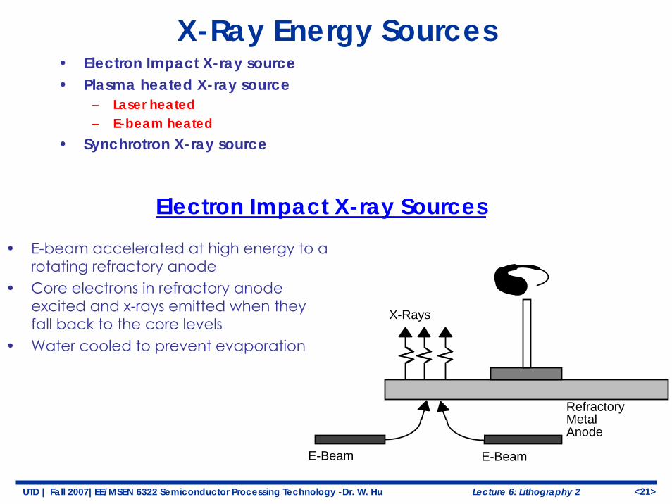
X-Ray Energy Sources• Electron Impact X-ray source• Plasma heated X-ray source
– Laser heated– E-beam heated
• Synchrotron X-ray source
• E-beam accelerated at high energy to a rotating refractory anode
• Core electrons in refractory anode excited and x-rays emitted when they fall back to the core levels
• Water cooled to prevent evaporation
X-Rays
E-Beam E-Beam
Refractory Metal Anode
Electron Impact X-ray Sources
UTD | Fall 2007|EE/MSEN 6322 Semiconductor Processing Technology -Dr. W. Hu <22>Lecture 6: Lithography 2
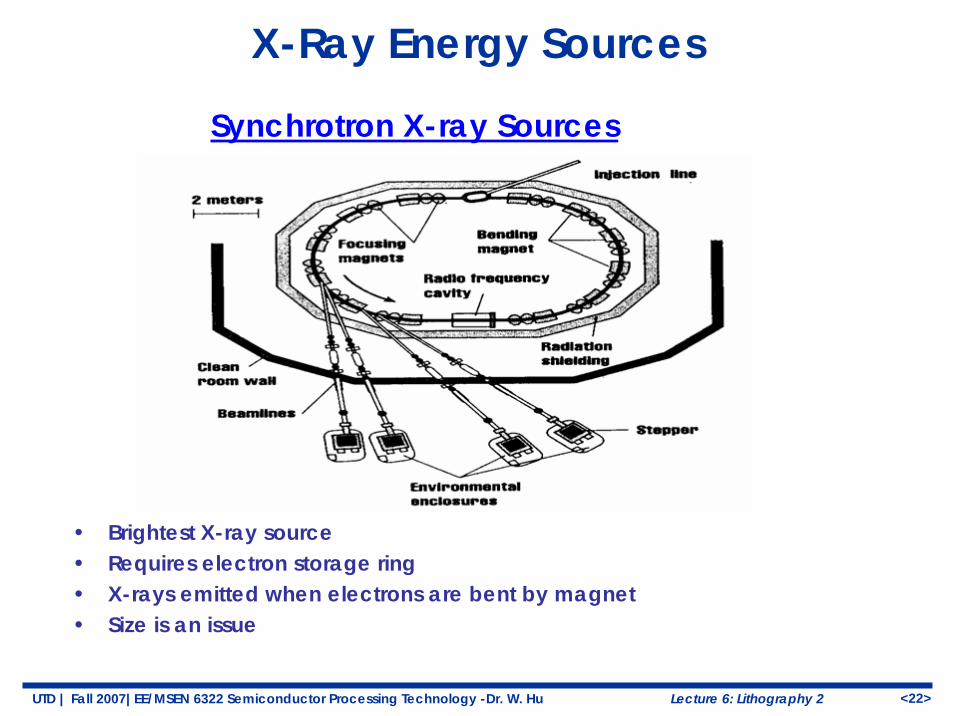
X-Ray Energy Sources
• Brightest X-ray source• Requires electron storage ring• X-rays emitted when electrons are bent by magnet• Size is an issue
Synchrotron X-ray Sources
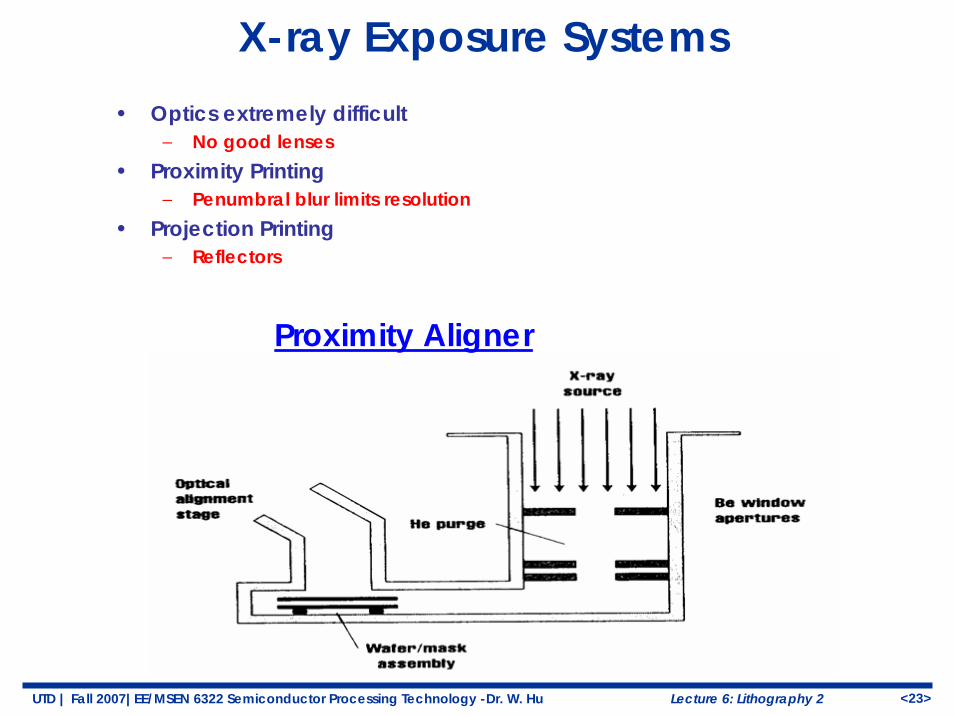
UTD | Fall 2007|EE/MSEN 6322 Semiconductor Processing Technology -Dr. W. Hu <23>Lecture 6: Lithography 2
X-ray Exposure Systems• Optics extremely difficult
– No good lenses• Proximity Printing
– Penumbral blur limits resolution• Projection Printing
– Reflectors
Proximity Aligner
UTD | Fall 2007|EE/MSEN 6322 Semiconductor Processing Technology -Dr. W. Hu <24>Lecture 6: Lithography 2
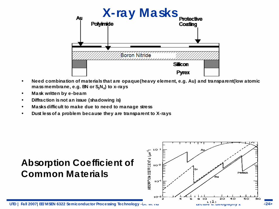
X-ray Masks
• Need combination of materials that are opaque(heavy element, e.g. Au) and transparent(low atomic mass membrane, e.g. BN or S3N4) to x-rays
• Mask written by e-beam• Diffraction is not an issue (shadowing is)• Masks difficult to make due to need to manage stress • Dust less of a problem because they are transparent to X-rays
Absorption Coefficient of Common Materials
UTD | Fall 2007|EE/MSEN 6322 Semiconductor Processing Technology -Dr. W. Hu <25>Lecture 6: Lithography 2
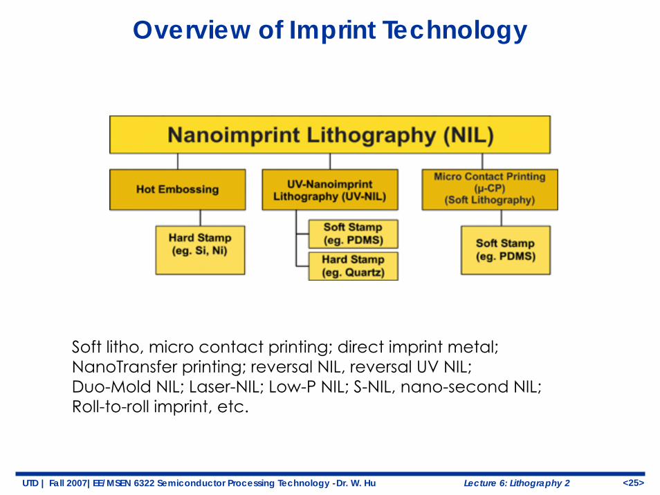
Overview of Imprint Technology
Soft litho, micro contact printing; direct imprint metal; NanoTransfer printing; reversal NIL, reversal UV NIL;Duo-Mold NIL; Laser-NIL; Low-P NIL; S-NIL, nano-second NIL; Roll-to-roll imprint, etc.
UTD | Fall 2007|EE/MSEN 6322 Semiconductor Processing Technology -Dr. W. Hu <26>Lecture 6: Lithography 2
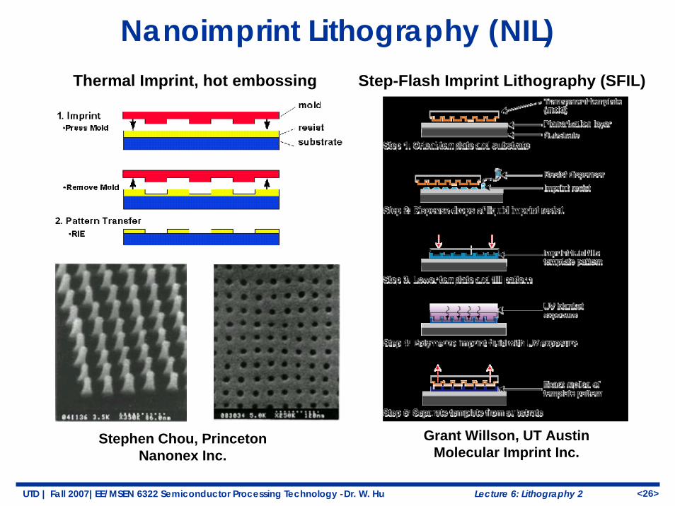
Nanoimprint Lithography (NIL)
Grant Willson, UT AustinMolecular Imprint Inc.
Stephen Chou, PrincetonNanonex Inc.
Step-Flash Imprint Lithography (SFIL)Thermal Imprint, hot embossing
UTD | Fall 2007|EE/MSEN 6322 Semiconductor Processing Technology -Dr. W. Hu <27>Lecture 6: Lithography 2
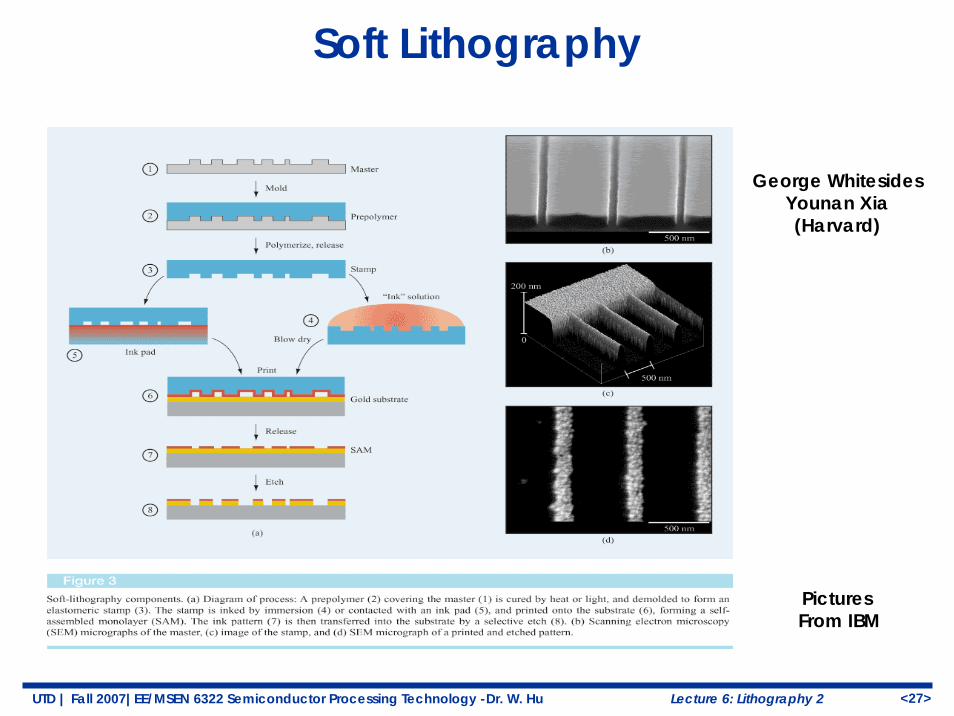
Soft Lithography
George WhitesidesYounan Xia(Harvard)
Pictures From IBM
UTD | Fall 2007|EE/MSEN 6322 Semiconductor Processing Technology -Dr. W. Hu <28>Lecture 6: Lithography 2
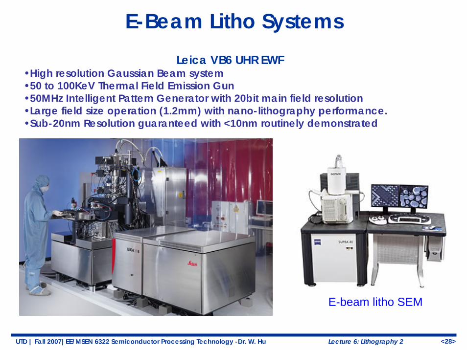
Leica VB6 UHR EWF•High resolution Gaussian Beam system •50 to 100KeV Thermal Field Emission Gun•50MHz Intelligent Pattern Generator with 20bit main field resolution•Large field size operation (1.2mm) with nano-lithography performance.•Sub-20nm Resolution guaranteed with <10nm routinely demonstrated
E-beam litho SEM
E-Beam Litho Systems
UTD | Fall 2007|EE/MSEN 6322 Semiconductor Processing Technology -Dr. W. Hu <29>Lecture 6: Lithography 2
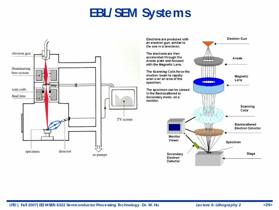
EBL/SEM Systems
UTD | Fall 2007|EE/MSEN 6322 Semiconductor Processing Technology -Dr. W. Hu <30>Lecture 6: Lithography 2
Electron Beam Sources
• Thermionic emitters– Electrons “boiled” off the surface by giving them thermal energy to overcome the
barrier (work function)– Current given by Richardson-Dushman Equation
• Field Emitters– Takes advantage of the quantum mechanical properties of electrons. – Electrons tunnel out when the surface barrier becomes very narrow– Current given by Fowler-Nordheim equation
• Photo Emitters– Energy given to electrons by incident radiation (photons)– Only photo-electrons generated close to the surface are able to escape
• Electrons extracted, collimated or focused and accelerated to 20 kV• Spot diameters of ≈50 Å can be achieved• Similar to ion-implantation
UTD | Fall 2007|EE/MSEN 6322 Semiconductor Processing Technology -Dr. W. Hu <31>Lecture 6: Lithography 2
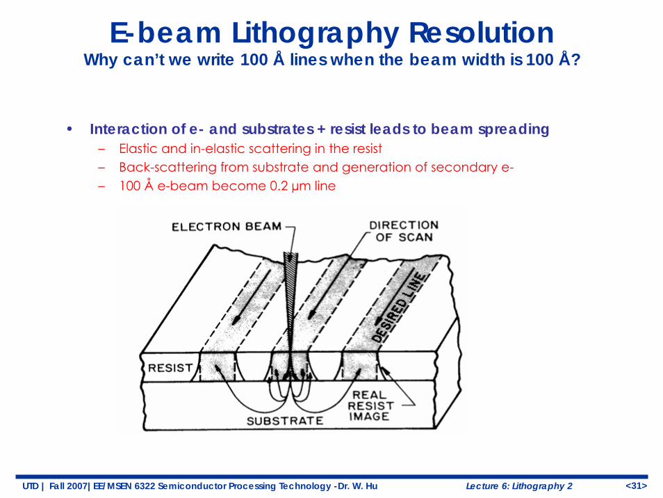
E-beam Lithography ResolutionWhy can’t we write 100 Å lines when the beam width is 100 Å?
• Interaction of e- and substrates + resist leads to beam spreading– Elastic and in-elastic scattering in the resist– Back-scattering from substrate and generation of secondary e-– 100 Å e-beam become 0.2 µm line


![2 LASER INTERFERENCE LITHOGRAPHY - uni-halle.de · 2 LASER INTERFERENCE LITHOGRAPHY (LIL) 9 2 LASER INTERFERENCE LITHOGRAPHY (LIL) Laser interference lithography [3~22] (LIL) is a](https://static.fdocuments.net/doc/165x107/5eae180eecc7e273a41a4e88/2-laser-interference-lithography-uni-hallede-2-laser-interference-lithography.jpg)