Lecture 5.0 Properties of Semiconductors. Importance to Silicon Chips Size of devices –Doping...
25
Lecture 5.0 Lecture 5.0 Properties of Semiconductors
-
Upload
diana-holmes -
Category
Documents
-
view
219 -
download
1
Transcript of Lecture 5.0 Properties of Semiconductors. Importance to Silicon Chips Size of devices –Doping...

Lecture 5.0Lecture 5.0
Properties of Semiconductors

Importance to Silicon ChipsImportance to Silicon Chips
Size of devices– Doping thickness/size– Depletion Zone Size– Electron Tunneling dimension
Chip Cooling- Device Density– Heat Capacity– Thermal Conductivity
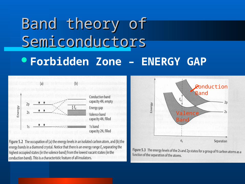
Band theory of SemiconductorsBand theory of Semiconductors
Forbidden Zone – ENERGY GAP
ValenceBand
ConductionBand

Silicon Band Structure - [Ne]3sSilicon Band Structure - [Ne]3s223p3p22

Fermi-Dirac Probability Fermi-Dirac Probability Distribution for electron energy, EDistribution for electron energy, E
Probability, F(E)=
(e{[E-Ef]/k
BT}+1)-1
–Ef is the
Fermi Energy

Number of Occupied StatesNumber of Occupied States
Fermi-Dirac
Density of States
T>0

Difference between Difference between Semiconductors and InsulatorsSemiconductors and Insulators
Material Eg(eV)
InSb 0.18
InAs 0.36
Ge 0.67
Si 1.12
GaAs 1.43
SiC 2.3
ZnS 3.6
NiO 4.2
Al2O3 8
kBT =0.0257 eV
at 298˚K

Probability of electrons in Probability of electrons in Conduction BandConduction Band
Lowest Energy in CBE-Ef Eg/2
Probability in CBF(E)= (exp{[E-Ef]/kBT} +1)-1 )
= (exp{Eg/2kBT} +1)-1
exp{-Eg/2kBT} for Eg>1 eV @ 298K
kBT =0.0257 eV
at 298˚K

Variation of Conductivity with TVariation of Conductivity with T=d/dT

Intrinsic Conductivity of Intrinsic Conductivity of SemiconductorSemiconductorCharge Carriers – Electrons– Holes
= ne e e + nh e h
# electrons = # holes ne e (e+ h)
– ne C exp{-Eg/2kBT} ne=2(2 m*e kBT/h2)3/2 exp(-Eg /(2kBT))Ef=Eg/2+3/4kBT ln(m*h/m*e)

MobilitiesMobilities

Semiconductor Photoelectric EffectSemiconductor Photoelectric EffectLight Absorption/Light Emission
(photodetector)/(photo diode laser)
Absorption max =hc/Eg

Light Emitting DiodeLight Emitting Diode

Photodiode LaserPhotodiode Laser
Color depends on band gap, Eg
=hc/Eg
Pb 0.37 0.27 0.33 IR detectors
Eg>3.0 transparent

Diode LaserDiode Laser

Extrinsic Conductivity of SemiconductorExtrinsic Conductivity of Semiconductor
Donor Doping Acceptor Dopingn-type p-type
p= 2(2 m*h kBT/h2)3/2 exp(-Ef/kBT)
Law of Mass Action, Nipi=ndpd or =nndn
N=nd+ni

Extrinsic Conductivity of SemiconductorExtrinsic Conductivity of Semiconductor
Donor Doping Acceptor Doping

Electron DensityElectron Density
Dopant Concentration effects Electron
DensityElectrical
Conductivity

ConductivityConductivity
Intrinsic Range– Exponential with T
Extrinsic Range– Promoted to CB
– Decreasing , – Joins Intrinsic
Majority/minority Carriers
= ne e e + nh e h

Majority/minority CarriersMajority/minority Carriers
Conductivity= ne e e + nh e h
n-type ne>>nh Low number of holes due to
recombination.Law of Mass Action
– Nipi=ndpd – (For p-type Nipi =nndn )

Extrinsic Conductivity of SemiconductorExtrinsic Conductivity of Semiconductor
Donor Doping Acceptor Dopingn-type p-type
Ed = -m*e e4/(8 (o)2 h2)Ef=Eg-Ed/2 Ef=Eg+Ea/2

Effective MassEffective Mass
HolesElectrons

Wafer SalesWafer Sales
Following PRIME GRADE Si wafers are all single-side polish $14.50 each for 25 wafers each $11.00 for 50 or more (we can double side polish)– 4" P<111> 3.0-6.6 ohm-cm– 4" N<100> 4.0-6.0 ohm-cm– 4" P<111> 7.0-21.6 ohm-cm– 4" P<100> 12.0-16.0 ohm-cm– 4" P<111> 3.0-5.0 ohm-cm
http://www.collegewafer.com/

GaP Wafer2" Undoped (100) $180.00 each 2" S doped (111) $180.00 each

C&ENews1/6/03