Lecture 4: Implementing Logic in CMOSusers.ece.utexas.edu/.../vlsi1/main/lectures/lecture_4.pdf ·...
32
VLSI-1 Class Notes Lecture 4: Implementing Logic in CMOS Mark McDermott Electrical and Computer Engineering The University of Texas at Austin 9/11/18
Transcript of Lecture 4: Implementing Logic in CMOSusers.ece.utexas.edu/.../vlsi1/main/lectures/lecture_4.pdf ·...

VLSI-1 Class Notes
Lecture 4:Implementing Logic in CMOS
Mark McDermottElectrical and Computer Engineering
The University of Texas at Austin
9/11/18
VLSI-1 Class Notes
Review of DeMorgan’s Theorem
Page 29/11/18
Recall that:(AB)’ = A’+B’ and AB = (A’ + B’)’(A+B) = A’B and A+B = (A’B’)’
AB
(AB)’ A’B’ A’+B’
AB AB A’
B’(A’+B’)’
AB
(A+B)’ A’B’
A’B’
AB A+B A’
B’(AB)’
VLSI-1 Class Notes
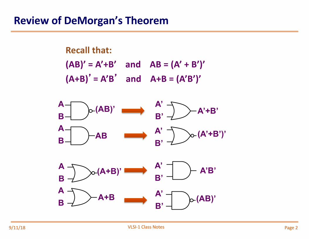
Bubble Pushing
§ Start with network of AND / OR gates§ Convert to NAND / NOR + inverters§ Push bubbles around to simplify logic
Y Y
Y
D
Y
(a) (b)
(c) (d)
Page 39/11/18
VLSI-1 Class Notes
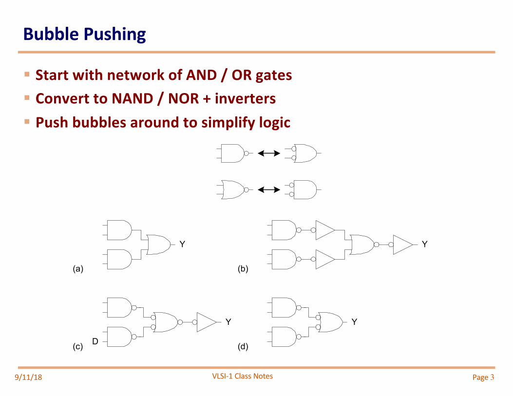
Static CMOS Circuits
§ N and P channel networks implement logic functions– Each network connected between Output and VDD or VSS
9/11/18
Series network: "AND" function
Parallel network: "OR" function
Page 4
VLSI-1 Class Notes
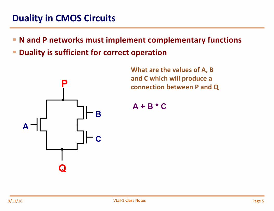
Duality in CMOS Circuits
§ N and P networks must implement complementary functions§ Duality is sufficient for correct operation
9/11/18
What are the values of A, B and C which will produce a connection between P and Q
AB
C
Q
P
A + B * C
Page 5

VLSI-1 Class Notes
Constructing Complex Gates
§ Example: F = (A * B) + (C * D)
– Take un-inverted function F = (AB + CD) and derive N-network
– Identify AND, OR components; F is OR of AB,CD
– Make connections of transistors
• AND , Series connection, OR , Parallel
Page 69/11/18
A
B
C
D
F
VLSI-1 Class Notes
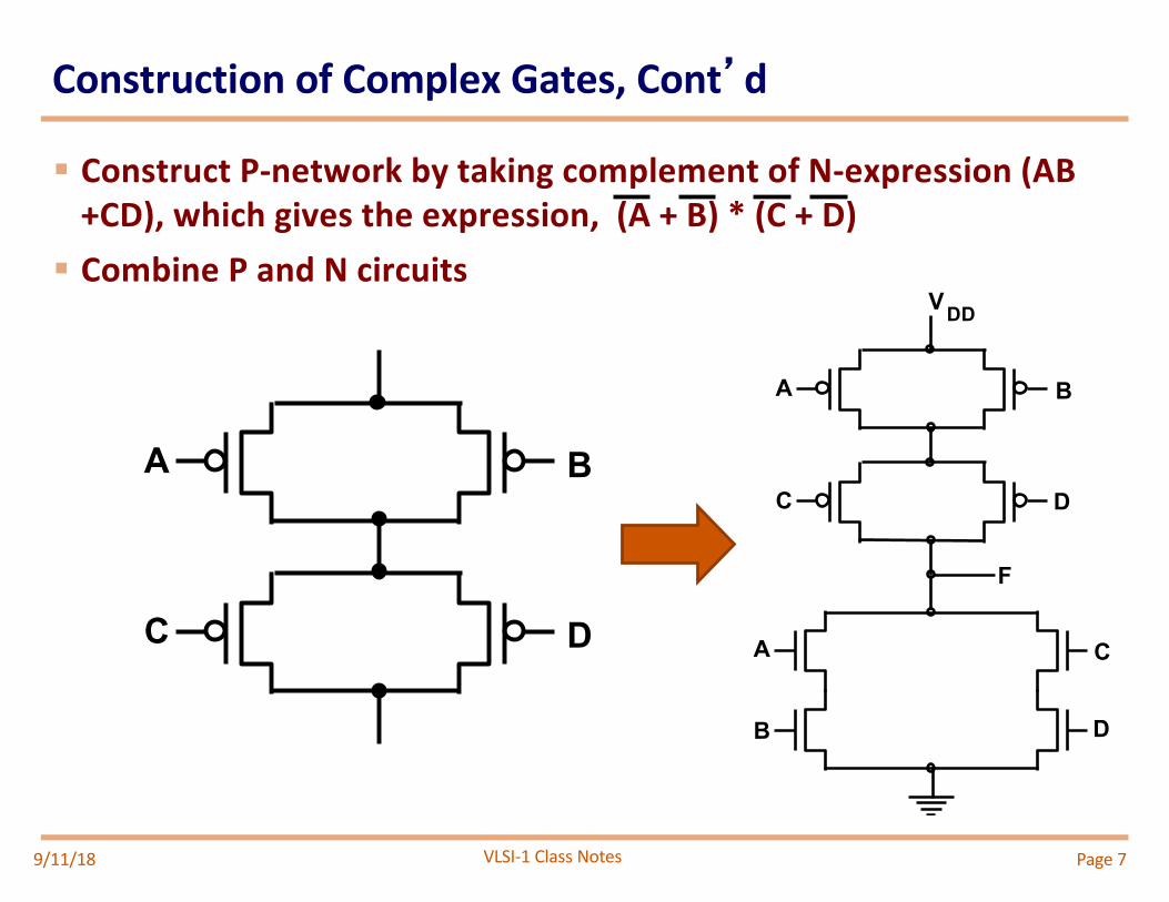
Construction of Complex Gates, Cont d
§ Construct P-network by taking complement of N-expression (AB +CD), which gives the expression, (A + B) * (C + D)
§ Combine P and N circuits
9/11/18
C D
A B
A B
C
F
V
D
DD
A
B
C
D
Page 7
VLSI-1 Class Notes
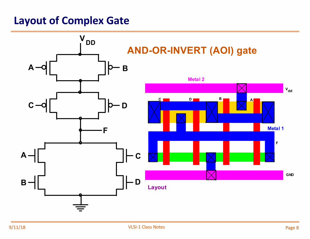
Layout of Complex Gate
9/11/18
A B
C
F
V
D
DD
A
B
C
D
AND-OR-INVERT (AOI) gate
C D B A
F
Vdd
GND
Layout
Metal 1
Metal 2
Page 8
VLSI-1 Class Notes
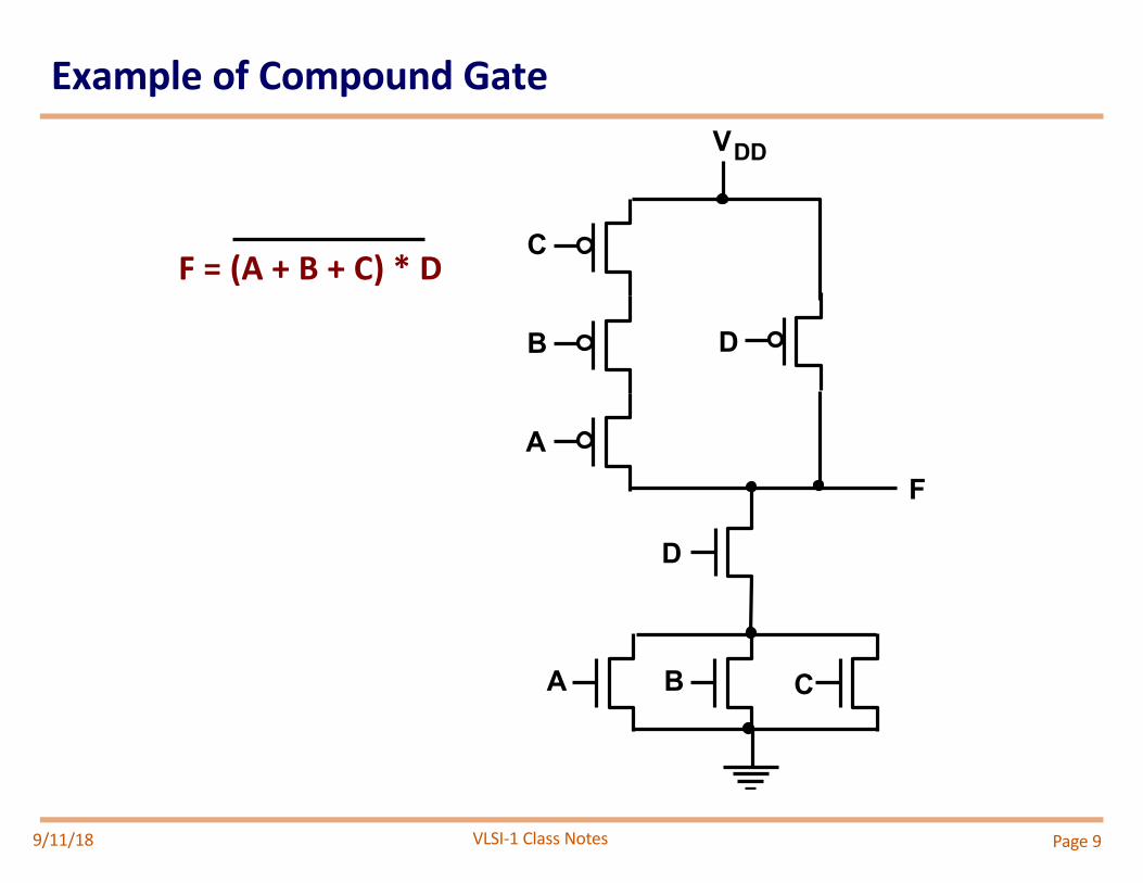
Example of Compound Gate
9/11/18
F = (A + B + C) * D
Page 9
V
C
B
A
D
D
A B C
DD
F
VLSI-1 Class Notes
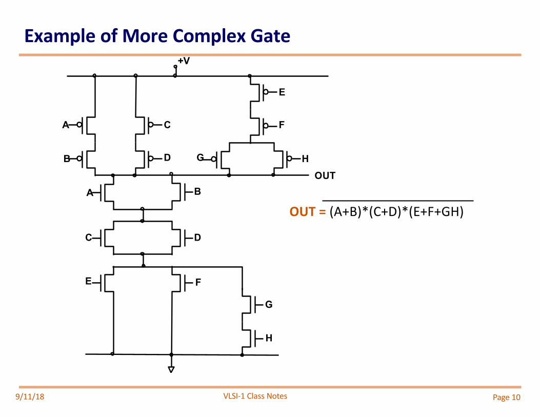
Example of More Complex Gate
9/11/18
A
B
C
E
D HG
F
BA
C D
E F
H
G
+V
OUT
Page 10
OUT = (A+B)*(C+D)*(E+F+GH)
VLSI-1 Class Notes
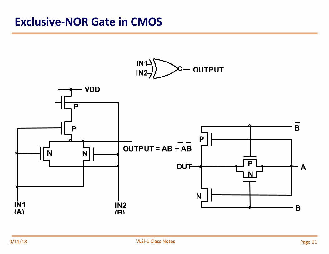
Exclusive-NOR Gate in CMOS
9/11/18
OUTPUTIN2IN1
VDD
P
P
IN1(A)
IN2(B)
N N OUTPUT = AB + AB
NB
OUT
P
PN
B
A
Page 11
VLSI-1 Class Notes
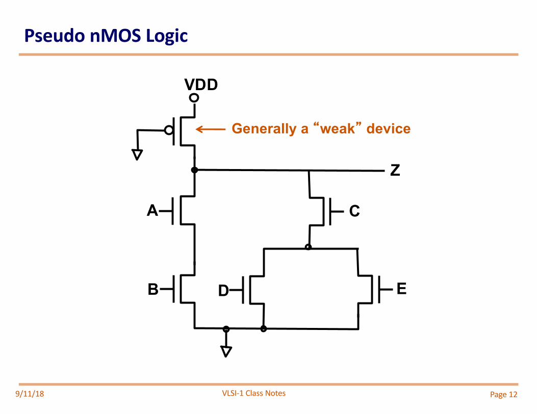
Pseudo nMOS Logic
9/11/18
VDD
B D
A
Z
C
E
Page 12
Generally a weak device
VLSI-1 Class Notes
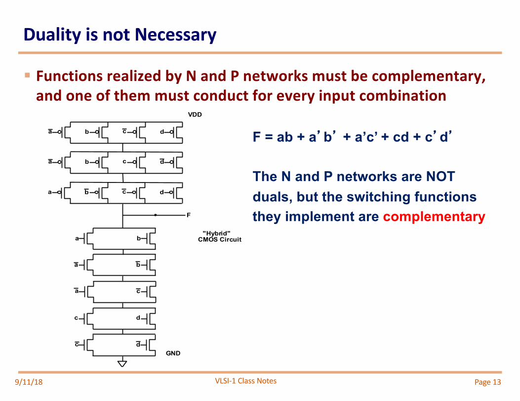
Duality is not Necessary
§ Functions realized by N and P networks must be complementary, and one of them must conduct for every input combination
9/11/18
da b c
da b c
da b c
VDD
F
CMOS Circuit"Hybrid"
a
b
c
b
a
a
c d
c dGND
F = ab + a b + a’c’ + cd + c d
The N and P networks are NOTduals, but the switching functionsthey implement are complementary
Page 13
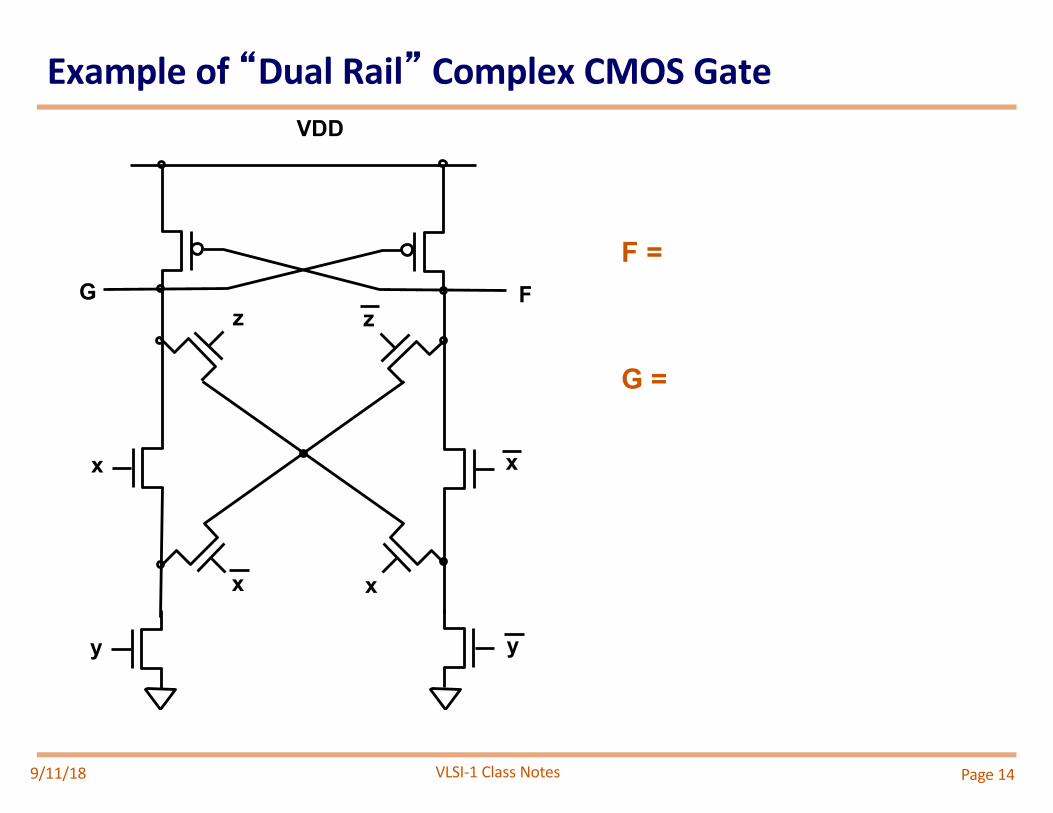
VLSI-1 Class Notes
Example of Dual Rail Complex CMOS Gate
9/11/18
F =
G =
VDD
G F
x x
y y
x x
zz
Page 14
VLSI-1 Class Notes
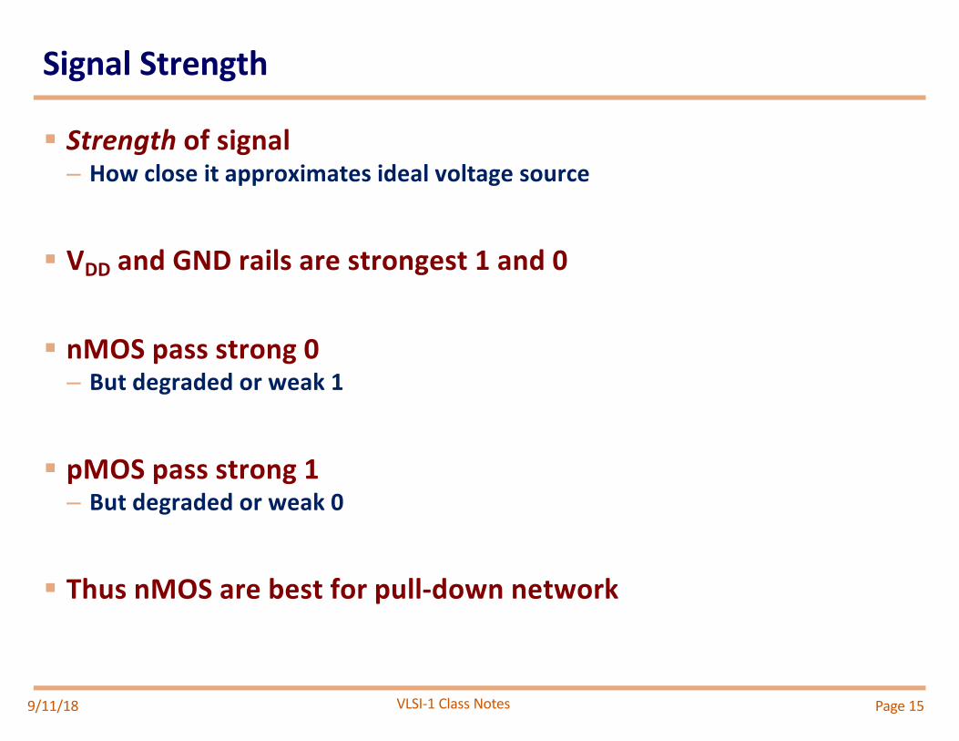
Signal Strength
§ Strength of signal– How close it approximates ideal voltage source
§ VDD and GND rails are strongest 1 and 0
§ nMOS pass strong 0– But degraded or weak 1
§ pMOS pass strong 1– But degraded or weak 0
§ Thus nMOS are best for pull-down network
9/11/18 Page 15

VLSI-1 Class Notes
Pass Transistors
§ Transistors can be used as switches
9/11/18
g
s d
g = 0s d
g = 1s d
0 strong 0Input Output
1 degraded 1
g
s d
g = 0s d
g = 1s d
0 degraded 0Input Output
strong 1
g = 1
g = 1
g = 0
g = 0
Page 16
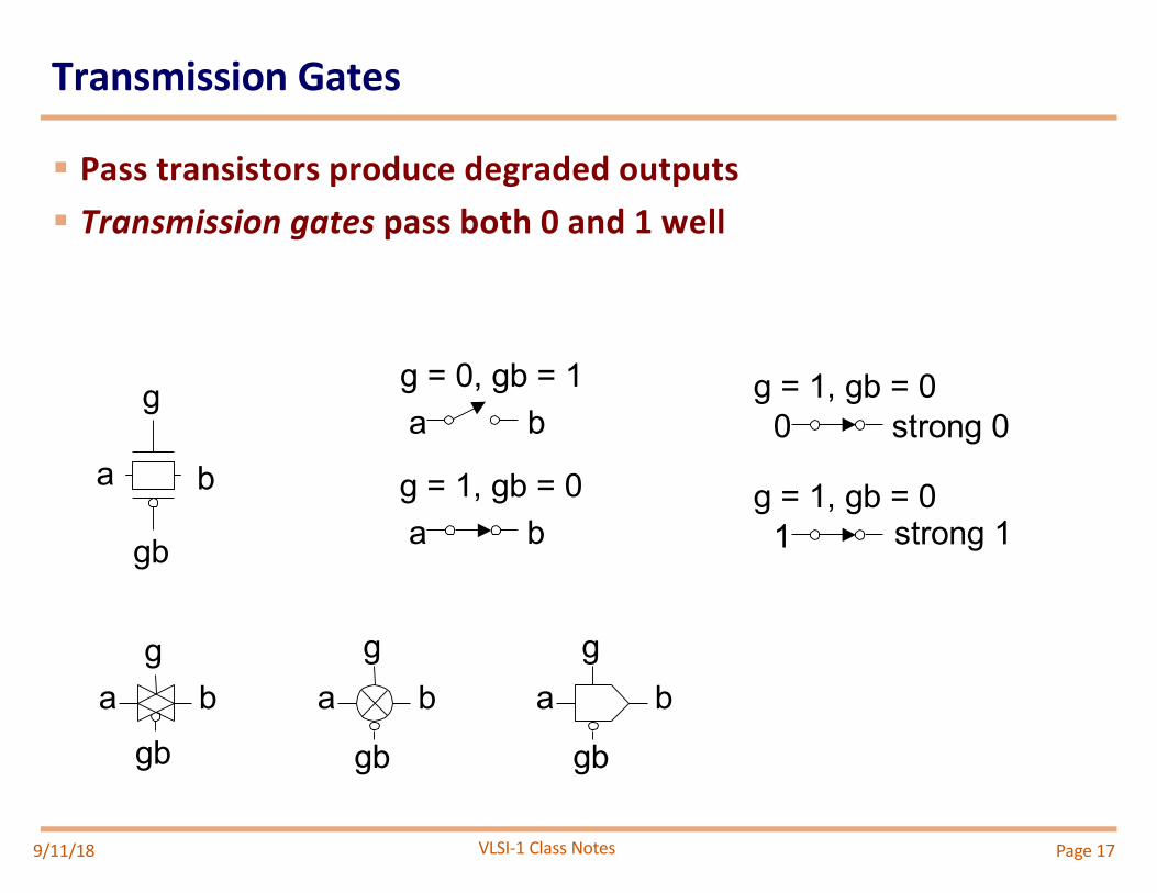
VLSI-1 Class Notes
Transmission Gates
§ Pass transistors produce degraded outputs§ Transmission gates pass both 0 and 1 well
9/11/18
g = 0, gb = 1a b
g = 1, gb = 0a b
0 strong 0
Input Output
1 strong 1
g
gb
a b
a bg
gba b
g
gb
a bg
gb
g = 1, gb = 0
g = 1, gb = 0
Page 17
VLSI-1 Class Notes
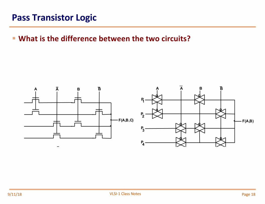
Pass Transistor Logic
§ What is the difference between the two circuits?
9/11/18
C, CF(A,B,C)
AA B B A B
F(A,B)
A B
P
P
P
P
1
2
3
4
Page 18
VLSI-1 Class Notes
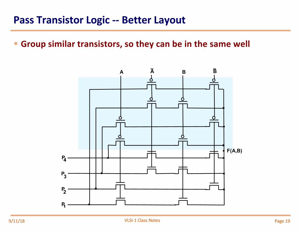
Pass Transistor Logic -- Better Layout
§ Group similar transistors, so they can be in the same well
9/11/18
A A B B
F(A,B)P
P
P
P
4
3
2
1
Page 19
VLSI-1 Class Notes
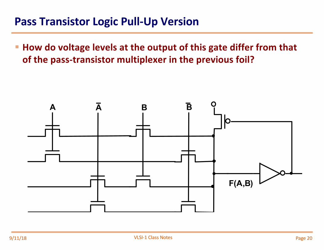
Pass Transistor Logic Pull-Up Version
§ How do voltage levels at the output of this gate differ from that of the pass-transistor multiplexer in the previous foil?
9/11/18
AA B B
F(A,B)
Page 20
VLSI-1 Class Notes
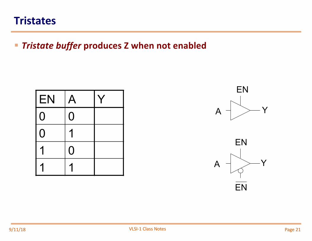
Tristates
§ Tristate buffer produces Z when not enabled
9/11/18
EN A Y0 00 11 01 1
A Y
EN
A Y
EN
EN
Page 21
VLSI-1 Class Notes
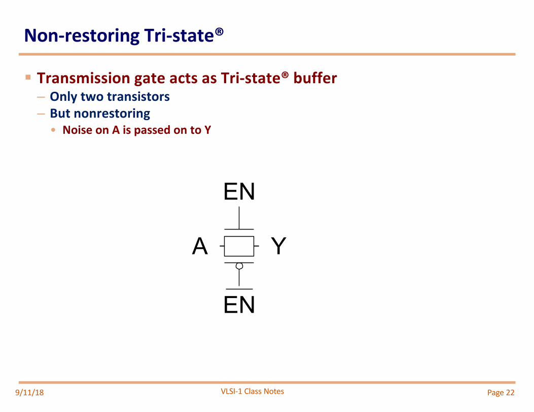
Non-restoring Tri-state®
§ Transmission gate acts as Tri-state® buffer– Only two transistors– But nonrestoring
• Noise on A is passed on to Y
9/11/18
A Y
EN
EN
Page 22
VLSI-1 Class Notes
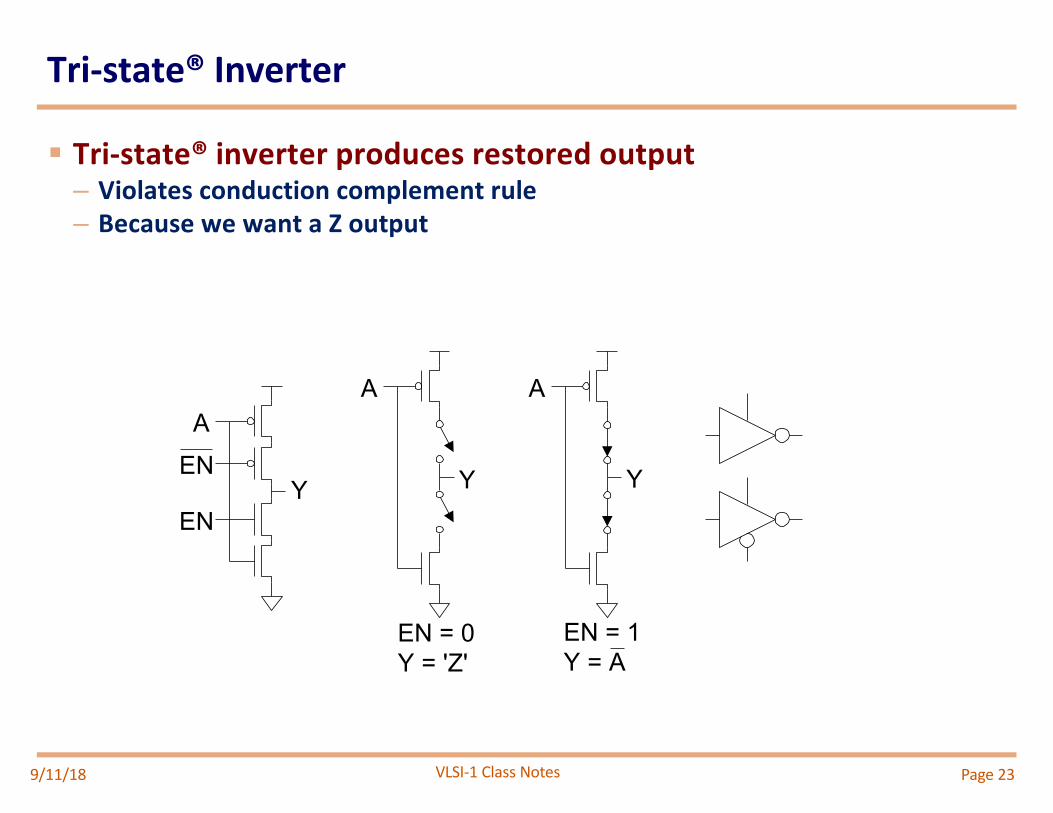
Tri-state® Inverter
§ Tri-state® inverter produces restored output– Violates conduction complement rule– Because we want a Z output
9/11/18
A
YEN
A
Y
EN = 0Y = 'Z'
Y
EN = 1Y = A
A
EN
Page 23
VLSI-1 Class Notes
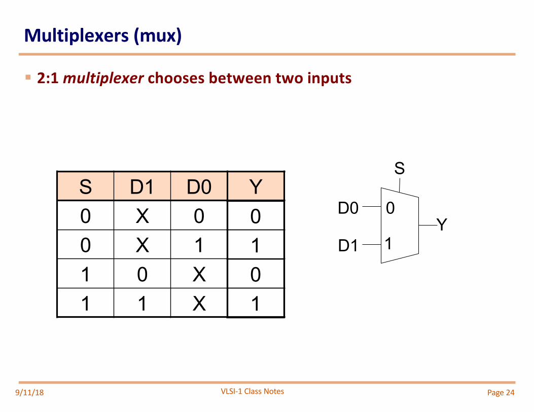
Multiplexers (mux)
§ 2:1 multiplexer chooses between two inputs
9/11/18
S D1 D0 Y0 X 00 X 11 0 X1 1 X
0
1
S
D0
D1Y
Page 24
0101
VLSI-1 Class Notes
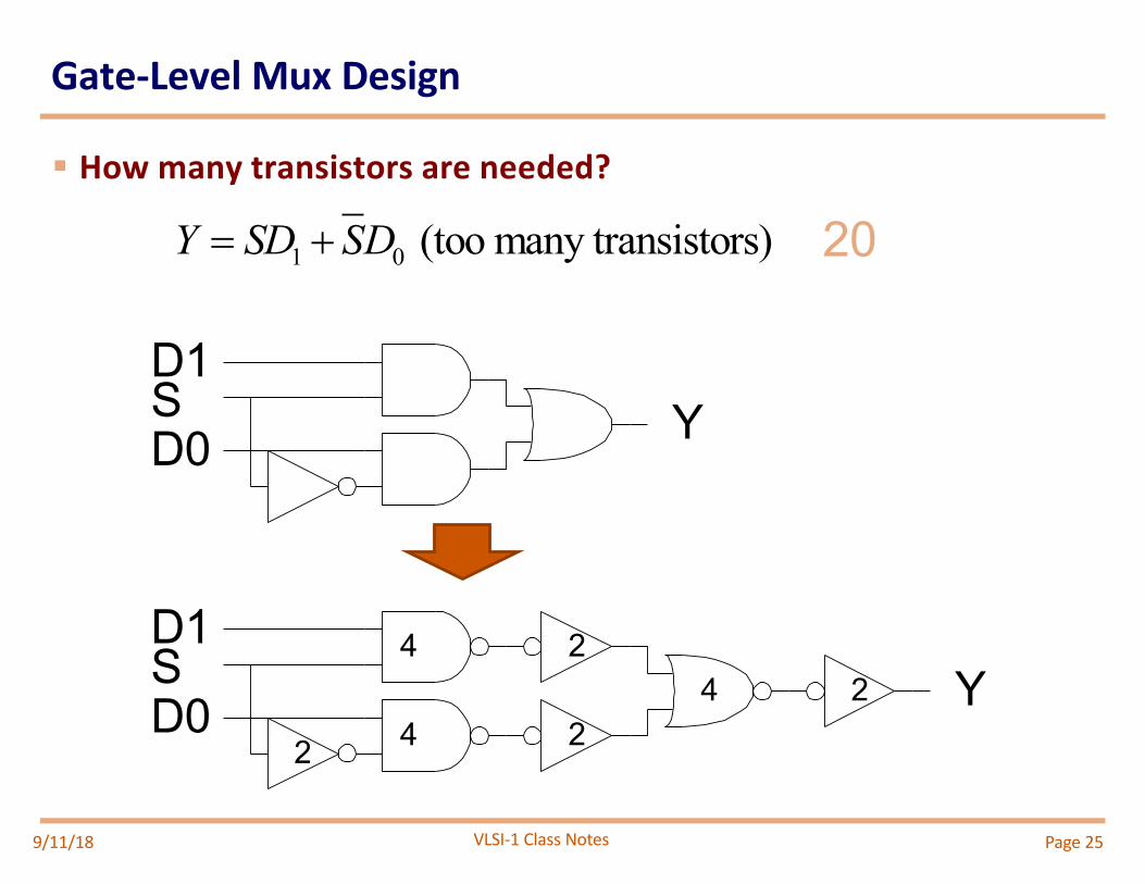
Gate-Level Mux Design
§ How many transistors are needed?
9/11/18
1 0 (too many transistors)Y SD SD= +
44
D1
D0S Y
4
2
22 Y
2
D1
D0S
20
Page 25
VLSI-1 Class Notes
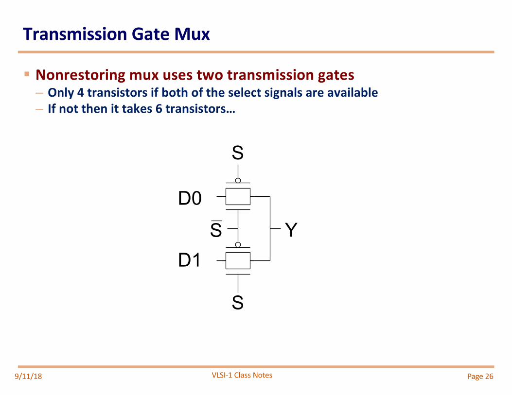
Transmission Gate Mux
§ Nonrestoring mux uses two transmission gates– Only 4 transistors if both of the select signals are available– If not then it takes 6 transistors…
9/11/18
S
S
D0
D1YS
Page 26

VLSI-1 Class Notes
Inverting Mux
§ Inverting multiplexer– Use compound AOI22– Or pair of tristate inverters– Essentially the same thing
§ Non-inverting multiplexer requires adding an inverter
9/11/18
SD0 D1
Y
S
D0
D1Y
0
1S
Y
D0D1
S
S
S
S
S
S
Page 27
VLSI-1 Class Notes
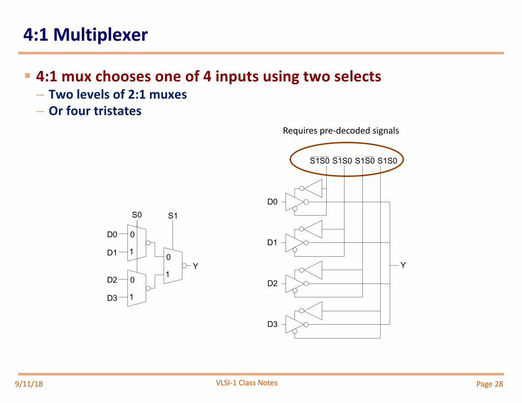
4:1 Multiplexer
§ 4:1 mux chooses one of 4 inputs using two selects– Two levels of 2:1 muxes– Or four tristates
9/11/18
S0
D0
D1
0
1
0
1
0
1Y
S1
D2
D3
D0
D1
D2
D3
Y
S1S0 S1S0 S1S0 S1S0
Page 28
Requires pre-decoded signals

VLSI-1 Class Notes
D Latch**
§ When CLK = 1, latch is transparent– D flows through to Q like a buffer
§ When CLK = 0, the latch is opaque– Q holds its old value independent of D
** transparent latch or level-sensitive latch
9/11/18
CLK
D Q
Latch D
CLK
Q
Page 29
VLSI-1 Class Notes
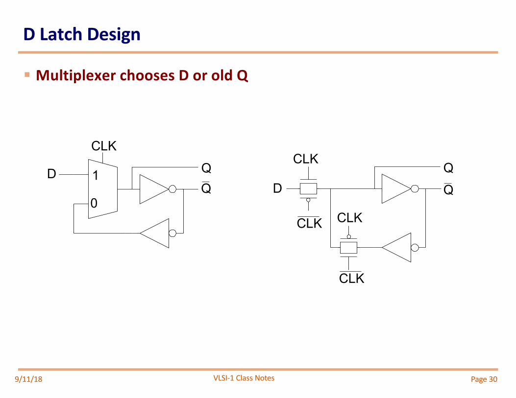
D Latch Design
§ Multiplexer chooses D or old Q
9/11/18
1
0
D
CLKQ
CLK
CLKCLK
CLK
DQ QQ
Page 30
VLSI-1 Class Notes
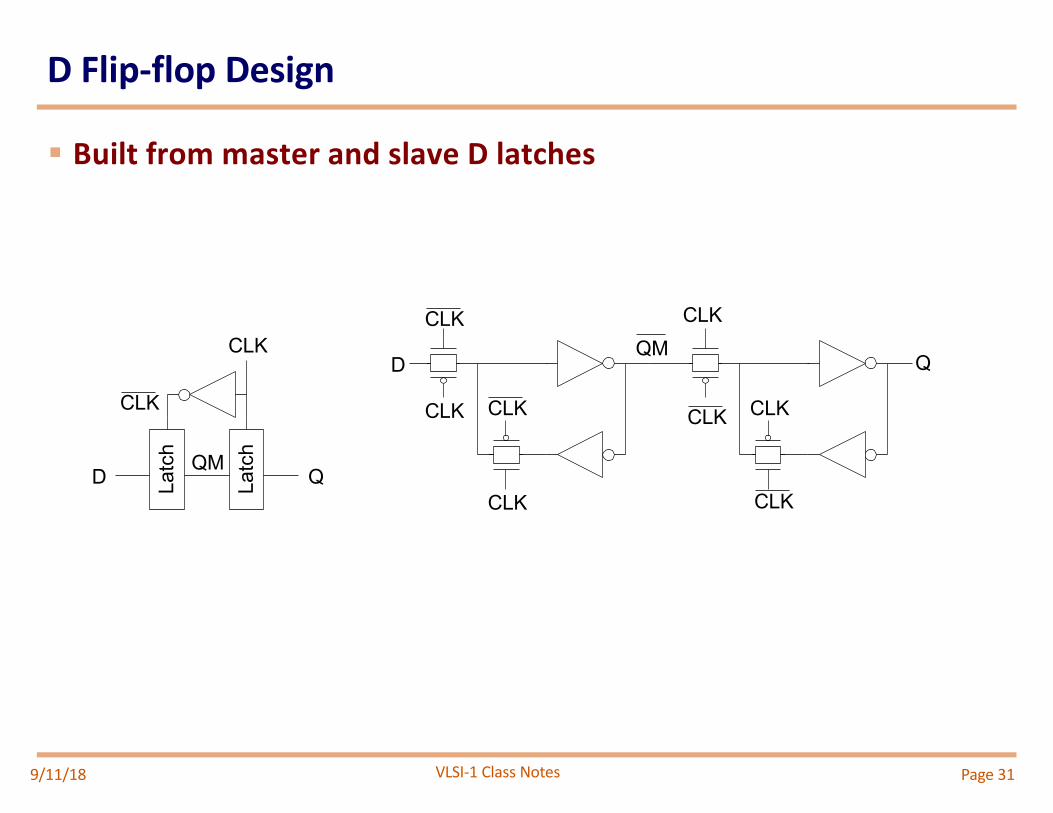
D Flip-flop Design
§ Built from master and slave D latches
9/11/18
QMCLK
CLKCLK
CLK
Q
CLK
CLK
CLK
CLK
D
Latch
Latch
D QQM
CLK
CLK
Page 31

VLSI-1 Class Notes
Questions?
9/11/18 Page 32