Lecture 4: Gate Leakage - Saraju Mohanty€¦ · Lecture 4: Gate Leakage . NOTE: ... not claim any...
84
CSCE 6933/5933 Advanced Topics in VLSI Systems Instructor: Saraju P. Mohanty, Ph. D. 1 Lecture 4: Gate Leakage NOTE: The figures, text etc included in slides are borrowed from various books, websites, authors pages, and other sources for academic purpose only. The instructor does not claim any originality. Advanced Topics in VLSI Systems
Transcript of Lecture 4: Gate Leakage - Saraju Mohanty€¦ · Lecture 4: Gate Leakage . NOTE: ... not claim any...
CSCE 6933/5933 Advanced Topics in VLSI Systems
Instructor: Saraju P. Mohanty, Ph. D.
1
Lecture 4: Gate Leakage
NOTE: The figures, text etc included in slides are borrowed from various books, websites, authors pages, and other sources for academic purpose only. The instructor does not claim any originality.
Advanced Topics in VLSI Systems
2
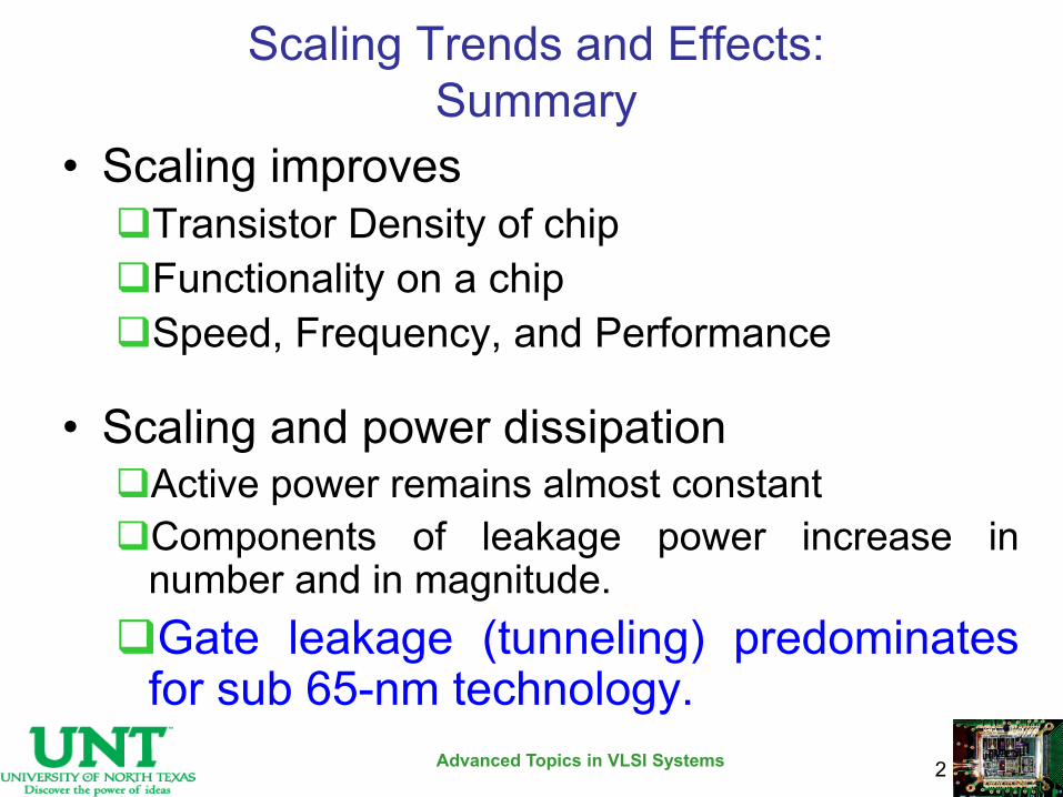
Scaling Trends and Effects: Summary
• Scaling improves Transistor Density of chip Functionality on a chip Speed, Frequency, and Performance
• Scaling and power dissipation Active power remains almost constant Components of leakage power increase in
number and in magnitude. Gate leakage (tunneling) predominates
for sub 65-nm technology. Advanced Topics in VLSI Systems
Advanced Topics in VLSI Systems
3
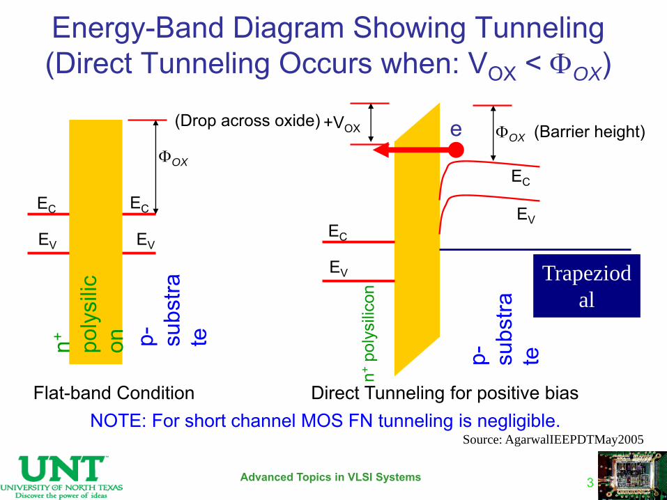
Energy-Band Diagram Showing Tunneling (Direct Tunneling Occurs when: VOX < FOX)
Source: AgarwalIEEPDTMay2005
Direct Tunneling for positive bias
e
n+ p
olys
ilico
n
EC
EV
p- subs
trate
EV
EC
+VOX FOX
EC
EV
Flat-band Condition
EV
n+
poly
silic
on
p- subs
trate
FOX
NOTE: For short channel MOS FN tunneling is negligible.
(Drop across oxide) (Barrier height)
Trapeziod
al
Potential
Barrier
EC

E. Kougianos and S. P. Mohanty, "Metrics to Quantify Steady and Transient Gate Leakage in Nanoscale Transistors: NMOS Vs PMOS Perspective", in Proceedings
of the 20th IEEE International Conference on VLSI Design
(VLSID), pp. 195-200, 2007.
Advanced Topics in VLSI Systems
4

5
Outline
1. Both ON and OFF state gate leakage are significant.
2. During transition of states there is transient effect is gate tunneling current.
3. Three metrics: ION, IOFF, and Ctunneling 4. Ctunneling: Manifests to intra-device loading effect of
the tunneling current. 5. NMOS Vs PMOS in terms of three metrics. 6. Study process/supply variation on three metrics.
Advanced Topics in VLSI Systems

6
Salient Point
The metric, effective tunneling capacitance essentially quantifies the intra-device loading effect of the tunneling current and also gives a qualitative idea of the driving capacity of a Nano-CMOS transistor.
Advanced Topics in VLSI Systems

7
Gate Capacitance of a Transistor (Intrinsic)
Advanced Topics in VLSI Systems
8
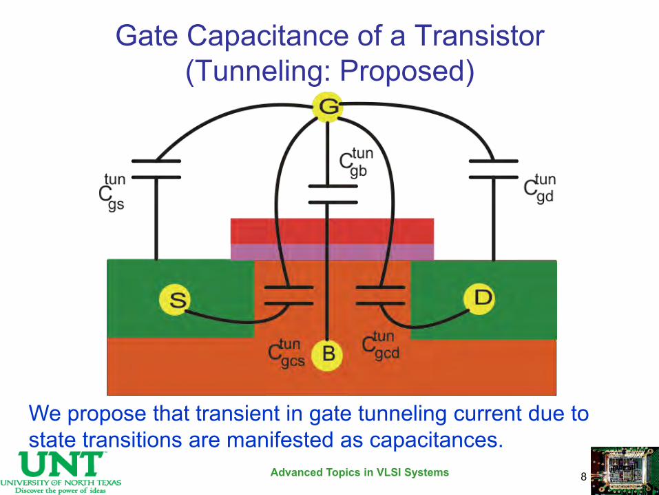
Gate Capacitance of a Transistor (Tunneling: Proposed)
We propose that transient in gate tunneling current due to state transitions are manifested as capacitances.
Advanced Topics in VLSI Systems

9
Analysis
in a Nano-CMOS Transistor
Advanced Topics in VLSI Systems
10
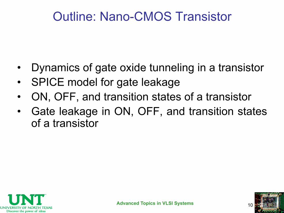
Outline: Nano-CMOS Transistor
• Dynamics of gate oxide tunneling in a transistor • SPICE model for gate leakage • ON, OFF, and transition states of a transistor • Gate leakage in ON, OFF, and transition states
of a transistor
Advanced Topics in VLSI Systems

11
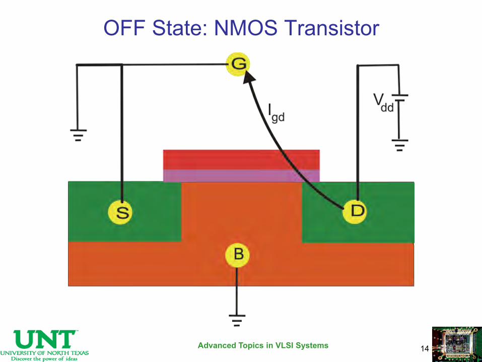
Gate Leakage Components (BSIM4 Model)
• Igs, Igd: tunneling through overlap of gate and diffusions • Igcs, Igcd: tunneling from the gate to the diffusions via channel • Igb: tunneling from the gate to the bulk via the channel
Advanced Topics in VLSI Systems

12
ON State: NMOS Transistor
Advanced Topics in VLSI Systems

13
ON State: PMOS Transistor
Advanced Topics in VLSI Systems
14
OFF State: NMOS Transistor
Advanced Topics in VLSI Systems

15
OFF State: PMOS Transistor
Advanced Topics in VLSI Systems

16
Transition State: NMOS Transistor
Advanced Topics in VLSI Systems

17
Transition State: PMOS Transistor
Advanced Topics in VLSI Systems

18
NMOS Gate Leakage Current (For a Switching Cycle)
Fig. 1
Fig. 2
Advanced Topics in VLSI Systems

19
PMOS Gate Leakage Current (For a Switching Cycle)
Fig. 1
Fig. 2
Advanced Topics in VLSI Systems

Advanced Topics in VLSI Systems
20
NMOS Vs PMOS: 3 Mechanisms of Tunneling
Source: Roy Proceedings of IEEE Feb2003
e
n+ p
olys
ilico
n
EC
EV
p-su
bstra
te EV
EC
+VOX FOX
h
JECB
JHVB
JEVB e
Three major mechanisms for direct tunneling: 1.electron tunneling from conduction band (ECB) 2.electron tunneling from valence band (EVB) 3.hole tunneling from valance band (HVB) For NMOS: •ECB controls gate-to-channel tunneling in inversion •EVB controls gate-to-body tunneling in depletion-inversion •ECB controls gate-to-body tunneling in accumulation For PMOS: •HVB controls the gate-to-channel tunneling in inversion •EVB controls gate-to-body tunneling in depletion-inversion •ECB controls gate-to-body tunneling in accumulation PMOS < NMOS: FOX for HVB (4.5 eV) is higher than FOX for ECB (3.1 eV), the tunneling current associated with HVB is less than that with ECB.

21
Three Metrics
for Tunneling Current
Advanced Topics in VLSI Systems

22
Gate Leakage: Observation
The behavior of the device in terms of gate tunneling leakage must be characterized not only during the steady states but also during transient states.
Advanced Topics in VLSI Systems
23
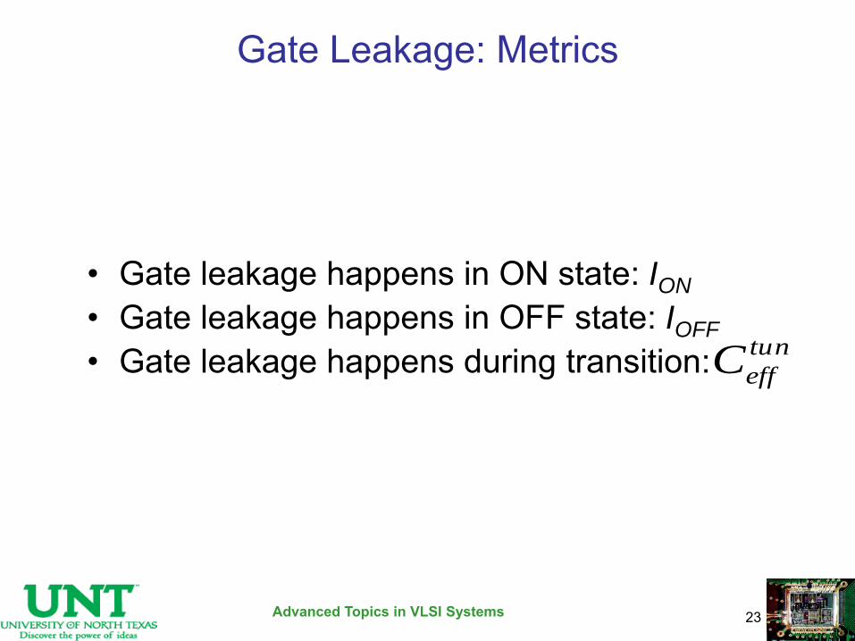
Gate Leakage: Metrics
• Gate leakage happens in ON state: ION
• Gate leakage happens in OFF state: IOFF
• Gate leakage happens during transition: tun
effC
Advanced Topics in VLSI Systems

24
Gate Leakage for a Transistor
Calculated by evaluating both the source and drain components
For a MOS, Iox = Igs +Igd +Igcs +Igcd +Igb
Values of individual components depends on states: ON, OFF, or transition
Advanced Topics in VLSI Systems

25
Gate Leakage Current (For a Switching Cycle)
For NMOS
For PMOS
Advanced Topics in VLSI Systems
26
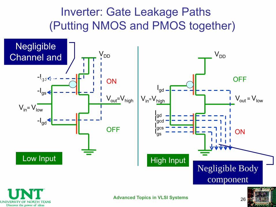
Inverter: Gate Leakage Paths (Putting NMOS and PMOS together)
High Input
Vout = Vlow
VDD
Vin=Vhigh
OFF
ON
Igd
Igd Igcd Igcs Igs
Low Input
VDD
Vout=Vhigh
ON
OFF
-Igd
-Igd
-Igs
Vin= Vlow
Negligible Channel and
Body components
Negligible Body
component
Advanced Topics in VLSI Systems
27
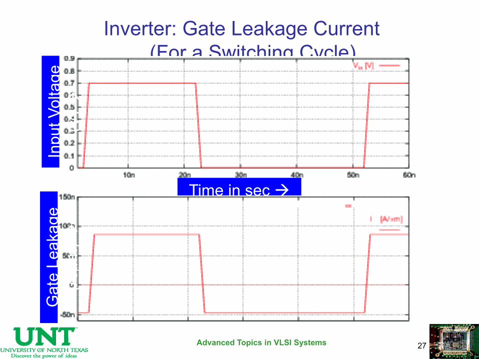
Inverter: Gate Leakage Current (For a Switching Cycle)
Time in sec
Inpu
t Vol
tage
(V
)
Gat
e Le
akag
e (A
/mm
)
Advanced Topics in VLSI Systems

28
Transient Gate Leakage:
tun
gcsCtun
gbCtun
gsC tunCgcd
tun
effC
tun
gdC
tun
effC
5 components
dt
dV
IIC
g
OFFONtun
eff
r
DD
OFFONt
V
II
We propose to quantify as:
(for equal rise/fall time)
Advanced Topics in VLSI Systems

29
Effect of
Process and Design Parameter Variation
Advanced Topics in VLSI Systems

30
ION / IOFF Versus Tox: NMOS
Gat
e Le
akag
e (A
/mm
)
Oxide Thickness (Tox)
Advanced Topics in VLSI Systems

31
ION / IOFF Versus Tox: PMOS
Oxide Thickness (Tox)
Gat
e Le
akag
e (A
/mm
)
Advanced Topics in VLSI Systems

32
ION / IOFF Versus Tox: Inverter G
ate
Leak
age
(A/m
m)
Oxide Thickness (Tox)
Advanced Topics in VLSI Systems

33
Versus Tox: NMOS tun
effC
Oxide Thickness (Tox)
Gat
e Le
akag
e (A
/mm
)
Advanced Topics in VLSI Systems

34
Versus Tox: PMOS tun
effC
Gat
e Le
akag
e (A
/mm
)
Oxide Thickness (Tox)
Advanced Topics in VLSI Systems

35
Versus Tox: Inverter tun
effC
Gat
e Le
akag
e (A
/mm
)
Oxide Thickness (Tox)
Advanced Topics in VLSI Systems

36
Statistical Analysis
of the Metrics
Advanced Topics in VLSI Systems

37
Monte Carlo Simulations: (Modeling Variations)
• Monte Carlo (N=1000) results. – 10% variation in gate oxide and supply assumed.
Advanced Topics in VLSI Systems

38
Monte Carlo Simulations: (Modeling Variations)
• All three metrics follow lognormal distribution. • This is expected since gate Tox and Vdd are
assumed normally distributed and Iox depends exponentially on both.
• Small parameter variation (10%) leads to large deviance in the metrics (2-3 sigma).
Advanced Topics in VLSI Systems

39
Gate Leakage in Nano-CMOS
• Both ON and OFF states contribute to gate oxide leakage.
• Transient effect is significant and can be captured via effective tunneling capacitance.
• ION and IOFF metrics to quantify gate leakage current during steady state.
• Cefftun ≡ Effective tunneling capacitance at the
input of a logic gate.
Advanced Topics in VLSI Systems
S. P. Mohanty and E. Kougianos, "Steady and Transient State Analysis of Gate Leakage Current in Nanoscale CMOS Logic Gates", in Proceedings of the 24th IEEE
International Conference on Computer Design (ICCD), pp. 210-215, 2006.
Advanced Topics in VLSI Systems
40

41
Outline
1. Both ON and OFF state gate leakage are significant.
2. During transition of states there is transient effect is gate tunneling current.
3. New metrics: Itun and Ctun 4. Ctun: Manifests to intra-device loading effect of the
tunneling current 5. NOR Vs NAND in terms of Itun and Ctun 6. Study process/design variation on Itun and Ctun
Advanced Topics in VLSI Systems

42
Salient Point
A new metric, the effective tunneling capacitance essentially quantifies the intra-device loading effect of the tunneling current and also gives a qualitative idea of the driving capacity of the logic gate. How to quantify it at transistor and logic-gate level??
Advanced Topics in VLSI Systems

43
Transistor Logic Gate
• How do we quantify the same metrics at logic level??
• State dependent or state independent??
Advanced Topics in VLSI Systems
44
Analysis
in Logic Gates
Advanced Topics in VLSI Systems
45
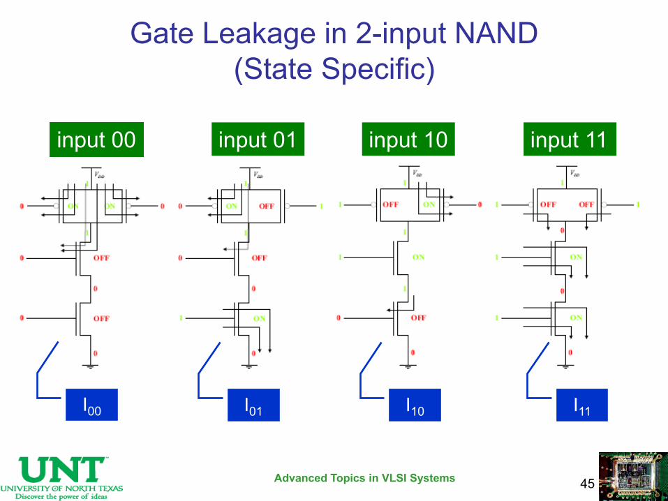
Gate Leakage in 2-input NAND (State Specific)
input 00 input 01 input 10 input 11
I00 I01 I10 I11
Advanced Topics in VLSI Systems

46
Gate Leakage in 2-input NAND (State Specific)
iMOS
ioxLogicox IStateI,
,, )(
00I 01I
Four different states for 2-input NAND:
11I
)(, StateI Logicox
10I
Advanced Topics in VLSI Systems
47
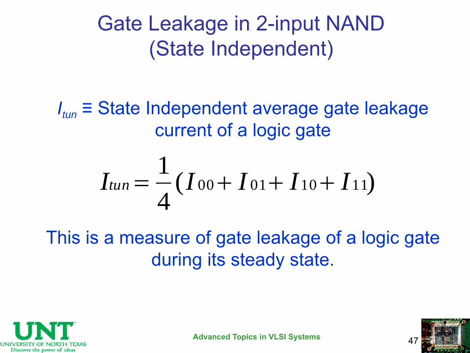
Gate Leakage in 2-input NAND (State Independent)
Itun ≡ State Independent average gate leakage current of a logic gate
)(4
111100100 IIIIItun
This is a measure of gate leakage of a logic gate during its steady state.
Advanced Topics in VLSI Systems
48
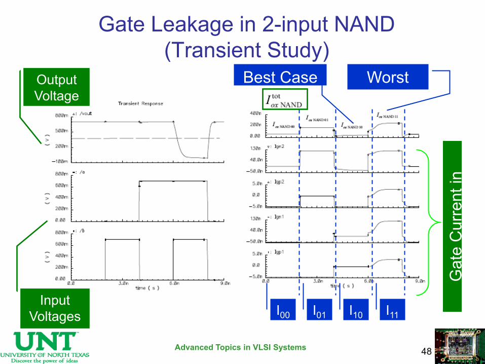
Gate Leakage in 2-input NAND (Transient Study)
Input Voltages
Output Voltage
I00 I01 I10 I11
Gat
e C
urre
nt in
in
divi
dual
MO
S
Best Case Worst Case
Advanced Topics in VLSI Systems

49
Gate Leakage in 2-input NOR (Transient Study)
Output Voltage
Input Voltages
Best Case
Worst Case
I00 I01 I10 I11
Gat
e C
urre
nt in
indi
vidu
al M
OS
Advanced Topics in VLSI Systems

50
Gate Leakage in Logic Gate (Transient Study)
Ctun ≡ Effective tunneling capacitance at the input of a logic gate
dt
dV
IIC
in
icictun
log
min
log
max
r
DD
icic
tV
II log
min
log
max
We propose to quantify as:
(for equal rise/fall time)
Advanced Topics in VLSI Systems

51
Effect of Process
and Design Parameter
Variation
Advanced Topics in VLSI Systems
52
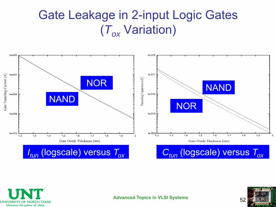
Gate Leakage in 2-input Logic Gates (Tox Variation)
Itun (logscale) versus Tox Ctun (logscale) versus Tox
NOR
NAND NOR
NAND
Advanced Topics in VLSI Systems
53
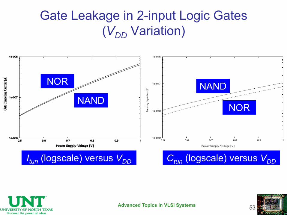
Gate Leakage in 2-input Logic Gates (VDD Variation)
Itun (logscale) versus VDD Ctun (logscale) versus VDD
NAND
NOR NAND
NOR
Advanced Topics in VLSI Systems

54
Observations
Advanced Topics in VLSI Systems

55
Gate Leakage in 2-input Logic Gates
• Both ON and OFF states contribute to gate leakage
• Transient effect is significant and can be captured via effective tunneling capacitance
• Itun ≡ State Independent average gate leakage current of a logic gate
• Ctun ≡ Effective tunneling capacitance at the input of a logic gate
• Itun is larger for NOR • Ctun is larger for NAND
Advanced Topics in VLSI Systems

56
Usefulness of the Proposed Metrics
• The metrics allow designers to account for gate tunneling effect in nano-CMOS based circuit designs.
• ION and IOFF - additive to static power consumption.
• Cefftun – additive to intrinsic gate capacitance
Clogic = Cefftun + Cintrinsic
• All three needs to be taken into account for effective total (switching, subthreshold, gate leakage) power optimization
Advanced Topics in VLSI Systems
57
Estimation of Gate Leakage
Advanced Topics in VLSI Systems
Advanced Topics in VLSI Systems
58
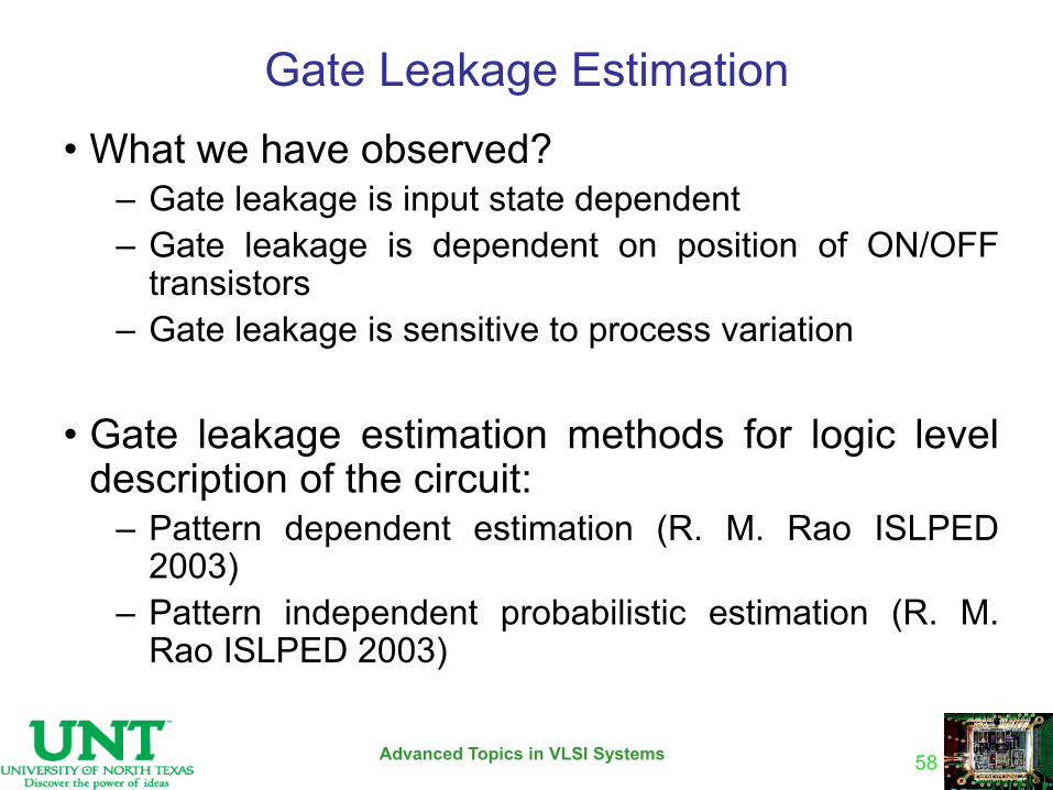
Gate Leakage Estimation • What we have observed?
– Gate leakage is input state dependent – Gate leakage is dependent on position of ON/OFF
transistors – Gate leakage is sensitive to process variation
• Gate leakage estimation methods for logic level
description of the circuit: – Pattern dependent estimation (R. M. Rao ISLPED
2003) – Pattern independent probabilistic estimation (R. M.
Rao ISLPED 2003)

Advanced Topics in VLSI Systems
59
Estimation: Pattern Dependent • For an given input vector switch-level simulation is
performed • State of internal nodes is determined for the input vector • Unit width gate leakage of a device is determined for
different states • The total gate leakage is computed by scaling the width
of each device by unit-width leakage in that state and adding the individual leakages:
Iox = SMOS Iox,MOS(s(i)) * WMOS
Source: R. M. Rao ISLPED2003

Advanced Topics in VLSI Systems
60
Estimation: Pattern Independent • Probability analysis in conjunction with state-
dependent gate leakage estimation is used. • The average gate leakage of the circuit is the
probabilistic mean of the gate leakage of the circuit:
Iox,avg = E(SMOS Iox,MOS(s(i)) * WMOS) = SMOS WMOS * ( Sj Iox,MOS(s(j)) * P(j) ) where P(j) is the probability of occurrence of
state j.
Source: R. M. Rao ISLPED2003
Advanced Topics in VLSI Systems
61
Estimation: Heuristic and Look-up Tables • Interaction between gate leakage and subthreshold
leakage are used to develop heuristic based estimation techniques for state-dependent total leakage current.
• Heuristics based on lookup tables are available to quickly estimate the state-dependent total leakage current for arbitrary circuit topologies.
Source: Lee ISQED2003, TVLSI2003
Advanced Topics in VLSI Systems
62
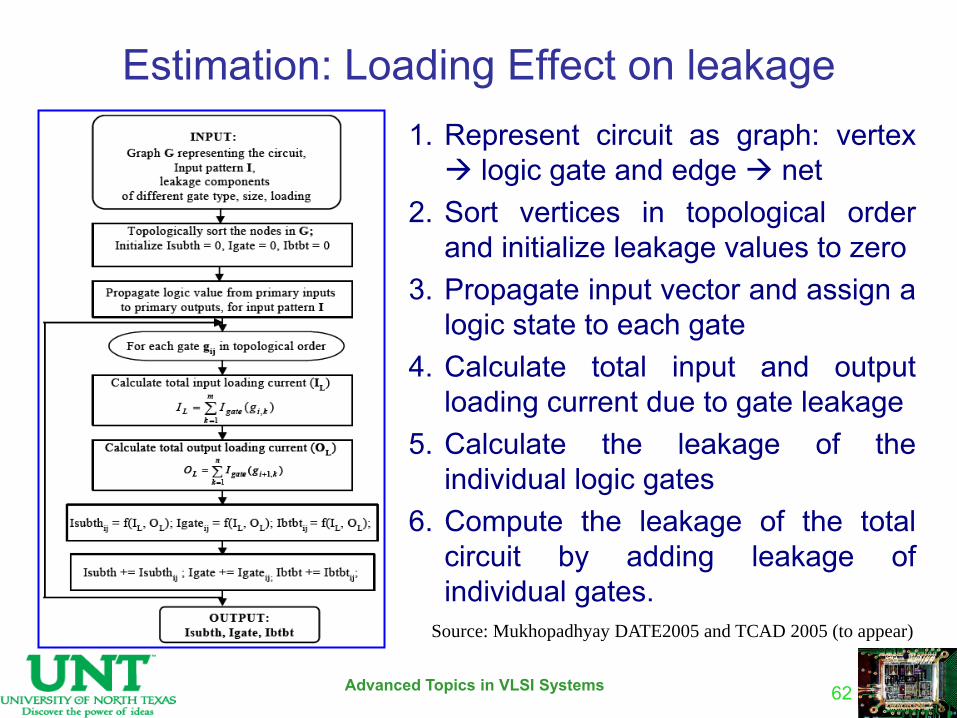
Estimation: Loading Effect on leakage 1. Represent circuit as graph: vertex logic gate and edge net
2. Sort vertices in topological order and initialize leakage values to zero
3. Propagate input vector and assign a logic state to each gate
4. Calculate total input and output loading current due to gate leakage
5. Calculate the leakage of the individual logic gates
6. Compute the leakage of the total circuit by adding leakage of individual gates.
Source: Mukhopadhyay DATE2005 and TCAD 2005 (to appear)

63
Optimization of Gate Leakage
Advanced Topics in VLSI Systems

Advanced Topics in VLSI Systems
64
Techniques for Gate Leakage Reduction
Research in Gate leakage is catching up and have not matured like that of dynamic or subthreshold power. Few methods: Dual TOX (Sultania DAC 2004, Sirisantana
IEEE DTC Jan-Feb 2004) Dual K (Mukherjee ICCD 2005) Pin and Transistor Reordering (Sultania ICCD
2004, Lee DAC 2003)

Advanced Topics in VLSI Systems
65
Dual TOX Technique: Basis
• Gate oxide tunneling current Ioxide (k is a experimentally derived factors):
Ioxide α (Vdd /Tgate)2 exp (– k Tgate/Vdd)
• Options for reduction of tunneling current: – Decreasing of supply voltage Vdd (will play its role) – Increasing gate SiO2 thickness Toxide

Advanced Topics in VLSI Systems
66
Dual TOX Technique: Basis
N+
P P
N+ N+ N+
High Tgate Low Tgate
Larger Igate , Smaller delay
Smaller Igate , Larger delay

Advanced Topics in VLSI Systems
67
Dual TOX Technique: Approach
Advantages: • Reduces DIBL effect • Constant Input Gate Capacitance for a given Weff,
Aspect Ratio = = constant
• Our approach – scale channel length (L) as well as Tox; Tox is almost linearly scaled with Leff
effox
eff
T
L
,
effox
effox
T
L
,
Cmicron = = constant

Advanced Topics in VLSI Systems
68
Critical path using STA
Dual TOX Technique: Algorithm
Assign all transistors to Tox-Hi
Compute cost = Leakage
Delay
Choose transistor with most negative cost
If no transistor chosen or Delay constraint
met, then EXIT
Assign Tox-Lo to chosen transistor and update
(always negative)
Source: Sultania DAC 2004

Advanced Topics in VLSI Systems
69
Dual TOX Technique: Results
• Iterative algorithm that – Generates delay/leakage tradeoffs – Meets delay constraint
• For same delay an average leakage reduction of 83% compared to the case where all transistors are set to Tox-Lo.
• Minor changes in design rules and an extra fabrication step is required, extra mask required.
Source: Sultania DAC 2004

Advanced Topics in VLSI Systems
70
Dual K Technique: Basis
N+
P P
N+ N+ N+
High Kgate Low Kgate Larger Igate ,
Smaller delay Smaller Igate , Larger delay

Advanced Topics in VLSI Systems
71
Dual K Technique: Basis
N+
P P
N+ N+ N+
High Tgate Low Tgate
Larger Igate , Smaller delay
Smaller Igate , Larger delay

Advanced Topics in VLSI Systems
72
Dual K Technique: Basis (Four Combinations of Kgate & Tgate)
P
P P
P N+
(1) K1T1
(4) K2T2 (3) K2T1
(2) K1T2
N+
N+ N+ N+ N+
N+ N+
Tunneling Current Delay
Advanced Topics in VLSI Systems
73
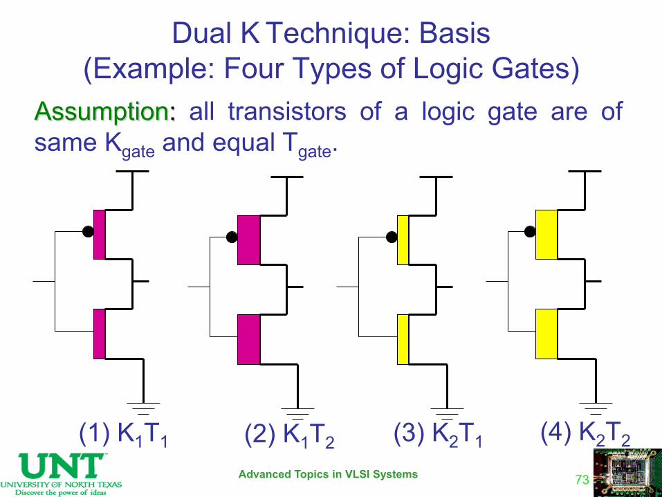
Dual K Technique: Basis (Example: Four Types of Logic Gates)
Assumption: all transistors of a logic gate are of same Kgate and equal Tgate.
(1) K1T1 (2) K1T2 (3) K2T1 (4) K2T2

Advanced Topics in VLSI Systems
74
Dual K Technique: Basis
Use of multiple dielectrics (denoted as Kgate) of multiple thickness (denoted as Tgate) will reduce the gate tunneling current significantly while maintaining the performance.
Source: Mukherjee ICCD 2005

Advanced Topics in VLSI Systems
75
Dual K Technique: New Dielectrics
• Silicon Oxynitride (SiOxNy) (K=5.7 for SiON) • Silicon Nitride (Si3N4) (K=7) • Oxides of :
– Aluminum (Al), Titanium (Ti), Zirconium (Zr), Hafnium (Hf), Lanthanum (La), Yttrium (Y), Praseodymium (Pr),
– their mixed oxides with SiO2 and Al2O3
• NOTE: Igate is still dependent on Tgate irrespective of dielectric material.
Advanced Topics in VLSI Systems
76
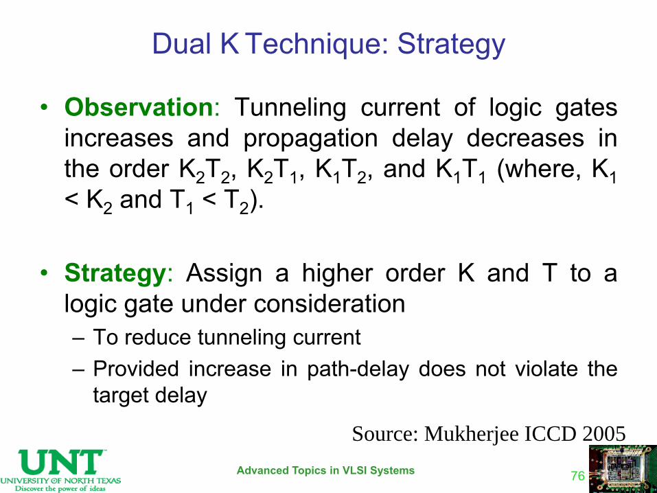
Dual K Technique: Strategy
• Observation: Tunneling current of logic gates increases and propagation delay decreases in the order K2T2, K2T1, K1T2, and K1T1 (where, K1 < K2 and T1 < T2).
• Strategy: Assign a higher order K and T to a
logic gate under consideration – To reduce tunneling current – Provided increase in path-delay does not violate the
target delay
Source: Mukherjee ICCD 2005

Advanced Topics in VLSI Systems
77
Dual K Technique: Algorithm
Step 1: Represent the network as a directed acyclic graph G(V, E).
Step 2: Initialize each vertex v G(V, E) with the
values of tunneling current and delay for K1T1 assignment.
Step 3: Find the set of all paths P{Pin} for all vertex
in the set of primary inputs (Pin), leading to the primary outputs Pout .
Step 4: Compute the delay DP for each path p
P{Pin}. Source: Mukherjee ICCD 2005
Advanced Topics in VLSI Systems
78
Dual K Technique: Algorithm
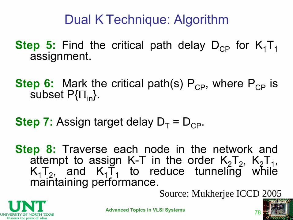
Step 5: Find the critical path delay DCP for K1T1 assignment.
Step 6: Mark the critical path(s) PCP, where PCP is
subset P{Pin}. Step 7: Assign target delay DT = DCP. Step 8: Traverse each node in the network and
attempt to assign K-T in the order K2T2, K2T1, K1T2, and K1T1 to reduce tunneling while maintaining performance.
Source: Mukherjee ICCD 2005

Advanced Topics in VLSI Systems
79
Dual K Technique: Characterization (How to Model High-K?)
• The effect of varying dielectric material was
modeled by calculating an equivalent oxide thickness (T*
ox) according to the formula: T*
ox = (Kgate / Kox) Tgate
• Here, Kgate is the dielectric constant of the gate dielectric material other than SiO2, (of thickness Tgate), while Kox is the dielectric constant of SiO2.

Advanced Topics in VLSI Systems
80
Dual K Technique: Characterization
• The effect of varying oxide thickness Tox was incorporated by varying TOXE in SPICE model.
• Length of the device is proportionately changed to minimize the impact of higher dielectric thickness on the device performance :
L* = (T*ox / Tox) L
• Length and width of the transistors are chosen to maintain (W:L) ratio of (4:1) for NMOS and (8:1) for PMOS.

Advanced Topics in VLSI Systems
81
Dual K Technique: Characterization
Igate Vs Thickness Igate Vs Dielectric Constant
Tpd Vs Thickness Tpd Vs Dielectric Constant
Source: Mukherjee ICCD 2005

Advanced Topics in VLSI Systems
82
Dual K Technique: Experimental Setup
• DKDT algorithm integrated with SIS, and tested on the ISCAS'85 benchmarks.
• Used K1 = 3.9 (for SiO2), K2 = 5.7 (for SiON), T1 = 1.4nm, and T2 = 1.7nm for our experiments.
• T1 is chosen as the default value from the BSIM4.4.0 model card and value of T2 is intuitively chosen
Source: Mukherjee ICCD 2005

Advanced Topics in VLSI Systems
83
Dual K Technique: Experimental Results Comparision of K1T1 Vs DKDT Assignment with %Reduction
05
10152025303540
C432
C499
C880
C1355
C1908
C2670
C3540
C5315
C6288
C7552
Benchmarks
Tunn
elin
g C
urre
nt in
m
icro
Am
ps
828486889092949698100
%R
educ
tion
K1T1DKDT%Reduction
Tunneling Current and % Reduction
Benchmark Circuits
Tunn
elin
g C
urre
nt ( m
A)
% R
eduction
Source: Mukherjee ICCD 2005

Advanced Topics in VLSI Systems
84
Pin Reordering with Dual-Tox A key difference between the state dependence of Isub and Igate • Isub primarily depends on the number of OFF in stack • Igate depends strongly on the position of ON/OFF transistors
Source: Sultania ICCD 2004
no transistor/ pin reordering
best possible pin reordering
best possible transistor reordering
best possible transistor and pin reordering
• Results improve by 5-10% compared to dual-Tox approach.