Lecture 22 Cascaded Systems and Combination BJT-FET...
23
Lecture 22 Cascaded Systems and Combination BJT-FET Circuits BJT-FET 1-1
Transcript of Lecture 22 Cascaded Systems and Combination BJT-FET...
Lecture 22
Cascaded Systems and Combination BJT-FET Circuits
BJT-FET 1-1
Outline
Introduction to Cascaded Amplifier Systems
Introduction to BJT-FET Combination Circuits
BJT-FET 1-2
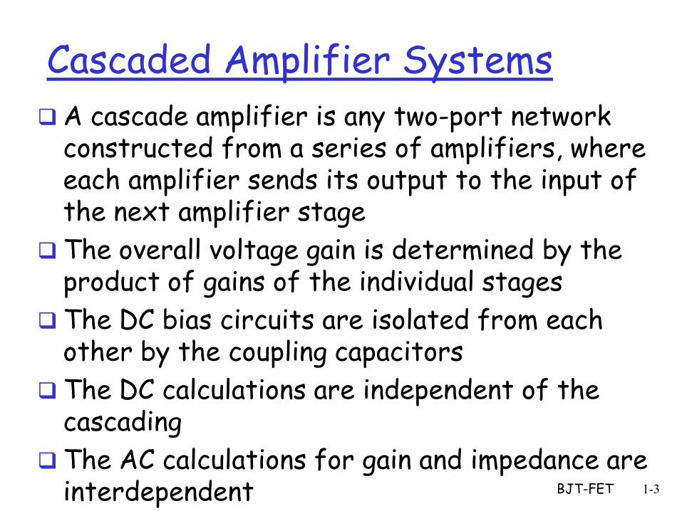
Cascaded Amplifier Systems
A cascade amplifier is any two-port network constructed from a series of amplifiers, where each amplifier sends its output to the input of the next amplifier stage
The overall voltage gain is determined by the product of gains of the individual stages
The DC bias circuits are isolated from each other by the coupling capacitors
The DC calculations are independent of the cascading
The AC calculations for gain and impedance are interdependent
BJT-FET 1-3
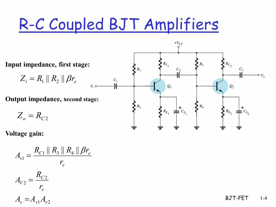
R-C Coupled BJT Amplifiers
BJT-FET 1-4
2Co RZ
Input impedance, first stage:
Output impedance, second stage:
Voltage gain:
ei rRRZ |||| 21
21
22
4311
||||||
vvv
e
CV
e
eCv
AAA
r
RA
r
rRRRA
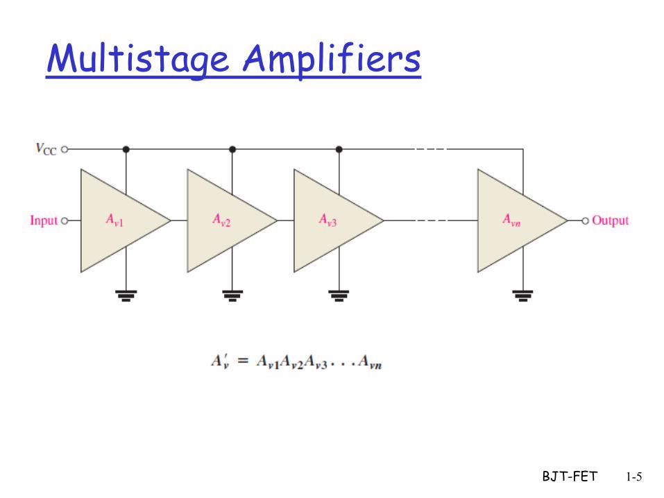
Multistage Amplifiers
BJT-FET 1-5
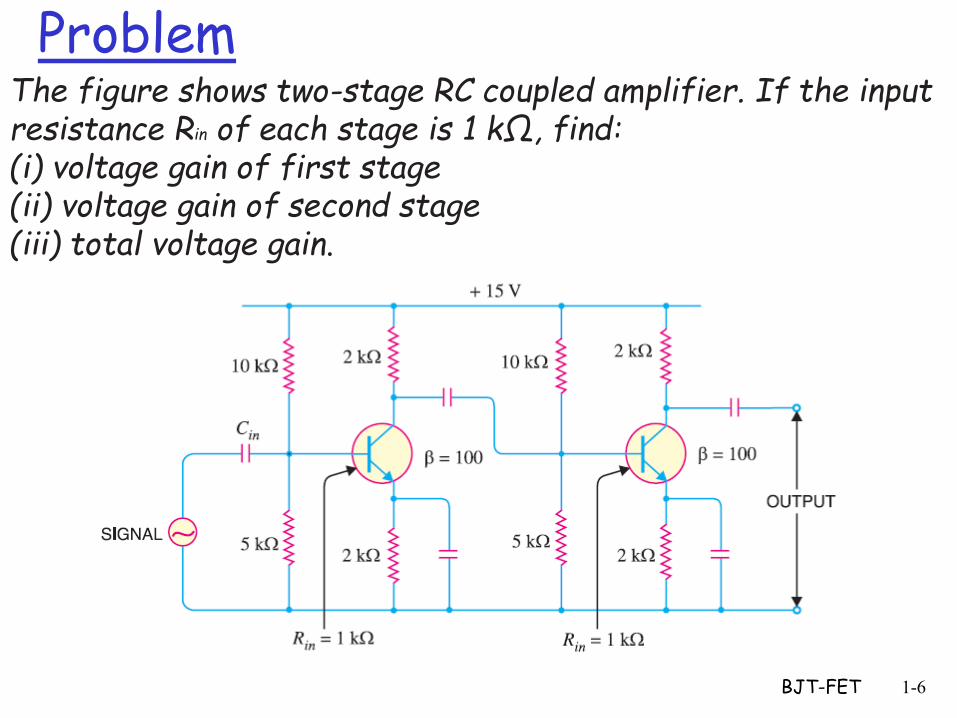
Problem
BJT-FET 1-6
The figure shows two-stage RC coupled amplifier. If the input resistance Rin of each stage is 1 kΩ, find: (i) voltage gain of first stage (ii) voltage gain of second stage (iii) total voltage gain.
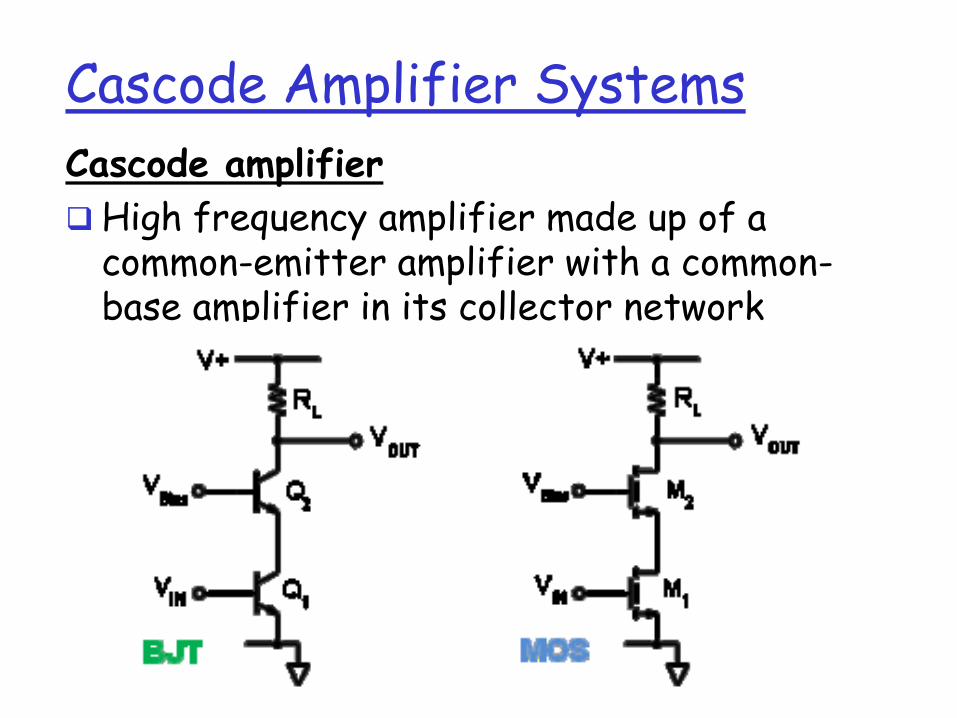
Cascode Amplifier Systems
Cascode amplifier
High frequency amplifier made up of a common-emitter amplifier with a common-base amplifier in its collector network
BJT-FET 1-7
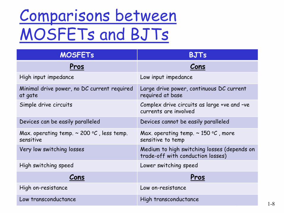
Comparisons between MOSFETs and BJTs
BJT-FET 1-8
MOSFETs BJTs
Pros Cons
High input impedance Low input impedance
Minimal drive power, no DC current required at gate
Large drive power, continuous DC current required at base
Simple drive circuits Complex drive circuits as large +ve and –ve currents are involved
Devices can be easily paralleled Devices cannot be easily paralleled
Max. operating temp. ~ 200 oC , less temp. sensitive
Max. operating temp. ~ 150 oC , more sensitive to temp
Very low switching losses Medium to high switching losses (depends on trade-off with conduction losses)
High switching speed Lower switching speed
Cons Pros
High on-resistance Low on-resistance
Low transconductance High transconductance
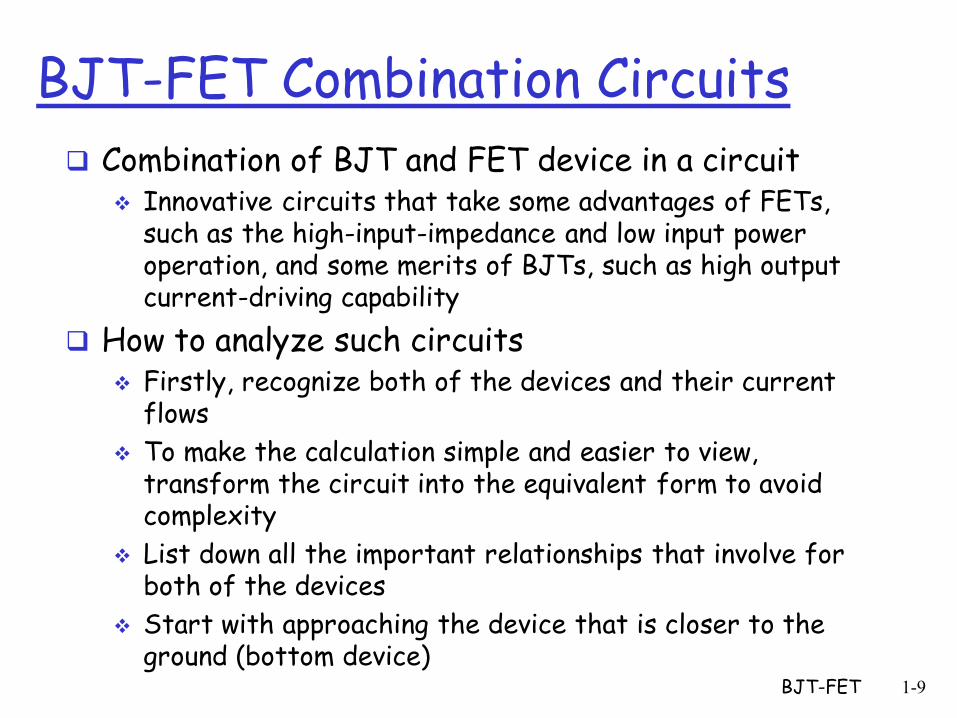
BJT-FET Combination Circuits
Combination of BJT and FET device in a circuit Innovative circuits that take some advantages of FETs,
such as the high-input-impedance and low input power operation, and some merits of BJTs, such as high output current-driving capability
How to analyze such circuits Firstly, recognize both of the devices and their current
flows
To make the calculation simple and easier to view, transform the circuit into the equivalent form to avoid complexity
List down all the important relationships that involve for both of the devices
Start with approaching the device that is closer to the ground (bottom device)
BJT-FET 1-9
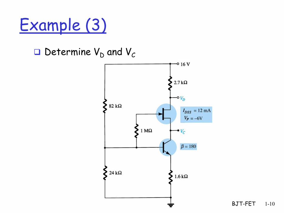
Example (3)
BJT-FET 1-10
Determine VD and VC
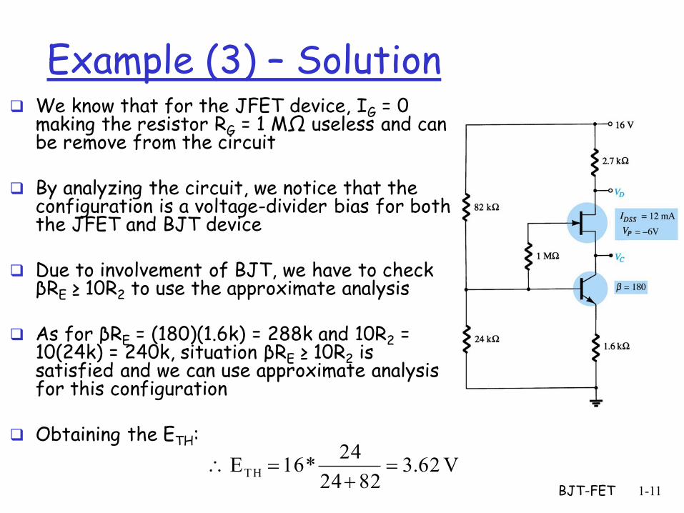
Example (3) – Solution
BJT-FET 1-11
We know that for the JFET device, IG = 0 making the resistor RG = 1 MΩ useless and can be remove from the circuit
By analyzing the circuit, we notice that the configuration is a voltage-divider bias for both the JFET and BJT device
Due to involvement of BJT, we have to check βRE ≥ 10R2 to use the approximate analysis
As for βRE = (180)(1.6k) = 288k and 10R2 = 10(24k) = 240k, situation βRE ≥ 10R2 is satisfied and we can use approximate analysis for this configuration
Obtaining the ETH:
V 62.38224
24*16ETH
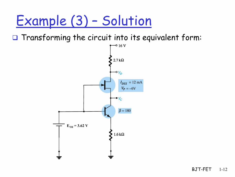
Example (3) – Solution
BJT-FET 1-12
ETH = 3.62 V
Transforming the circuit into its equivalent form:
ETH = 3.62 V
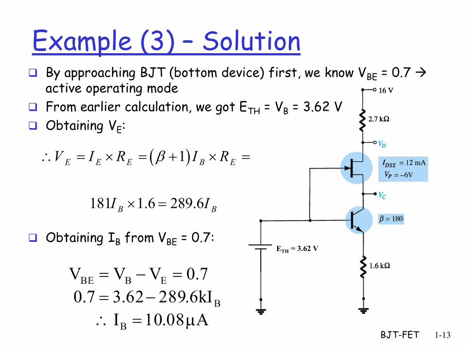
Example (3) – Solution
BJT-FET 1-13
By approaching BJT (bottom device) first, we know VBE = 0.7 active operating mode
From earlier calculation, we got ETH = VB = 3.62 V
Obtaining VE:
Obtaining IB from VBE = 0.7:
1
181 1.6 289.6
E E E B E
B B
V I R I R
I I
A 08.10I
kI6.28962.37.0
7.0VVV
B
B
EBBE
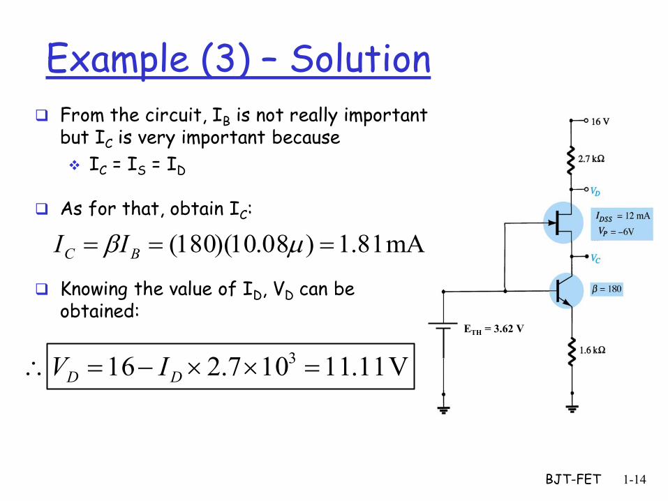
Example (3) – Solution
BJT-FET 1-14
From the circuit, IB is not really important but IC is very important because
IC = IS = ID
As for that, obtain IC:
Knowing the value of ID, VD can be obtained:
mA 81.1)08.10)(180( BC II
V 11.11107.216 3 DD IV
ETH = 3.62 V
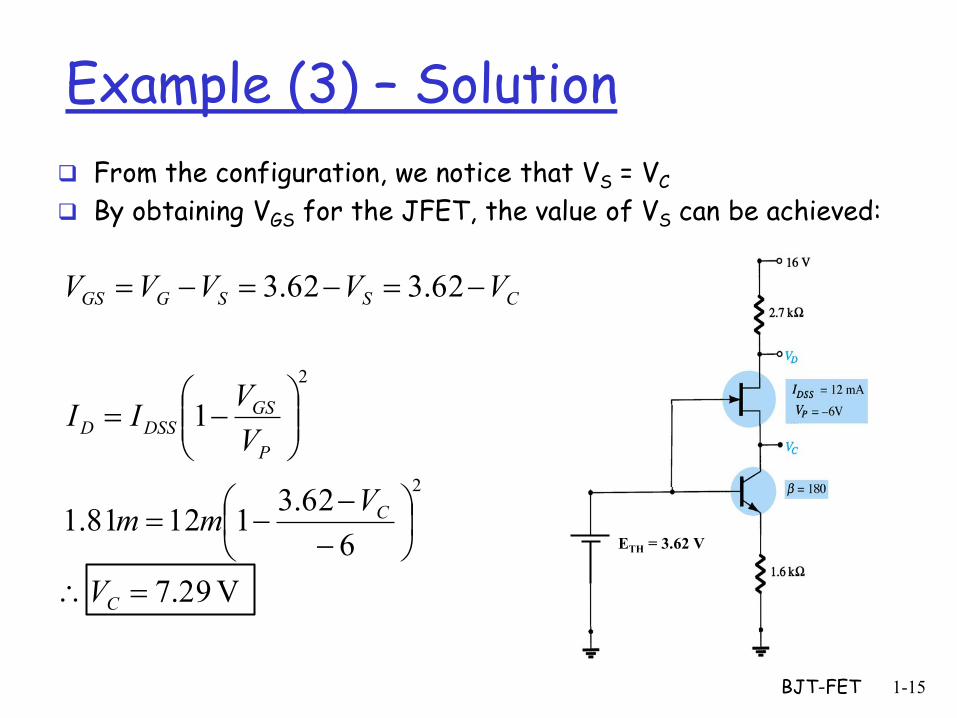
Example (3) – Solution
BJT-FET 1-15
From the configuration, we notice that VS = VC
By obtaining VGS for the JFET, the value of VS can be achieved:
V 29.7
6
62.311281.1
1
62.362.3
2
2
C
C
P
GSDSSD
CSSGGS
V
Vmm
V
VII
VVVVV
ETH = 3.62 V

The Darlington Pair
BJT-FET 1-16
- The Darlington circuit provides a very high current gain—the product of the individual current gains:
D = 12
- The practical significance is that the circuit provides a very high input impedance.
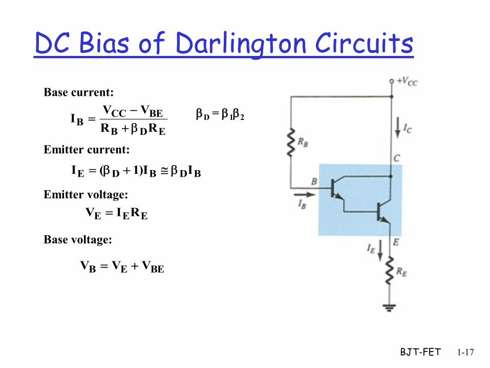
DC Bias of Darlington Circuits
BJT-FET 1-17
BDBDE II)1(I
EEE RIV
EDB
BECCB
RR
VVI
Base current:
Emitter current:
Emitter voltage:
Base voltage:
BEEB VVV
D = 12
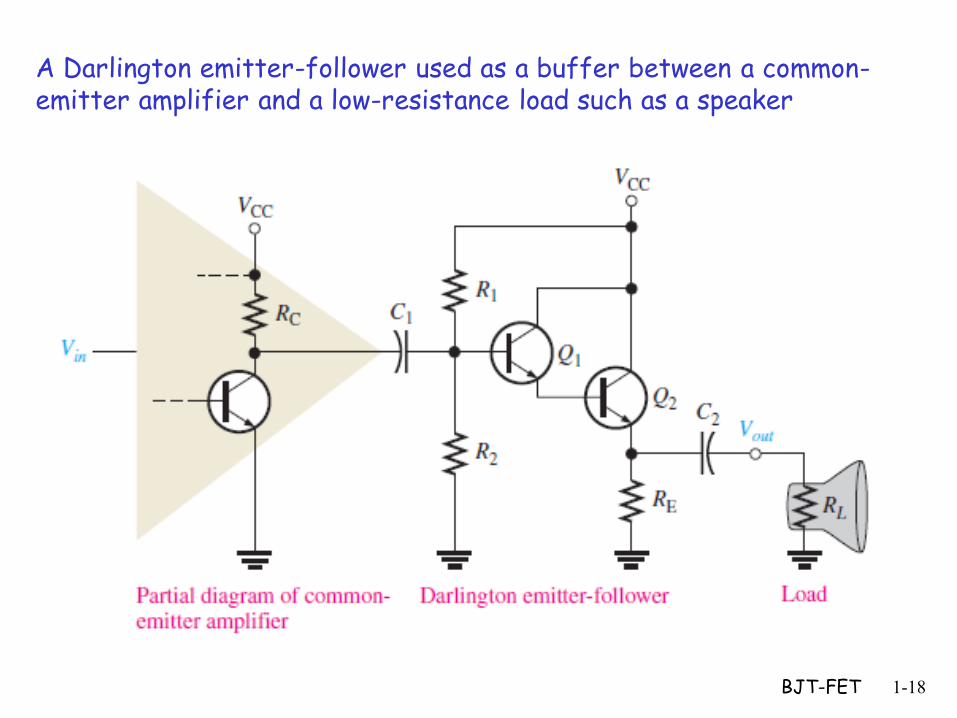
A Darlington emitter-follower used as a buffer between a common-emitter amplifier and a low-resistance load such as a speaker
BJT-FET 1-18
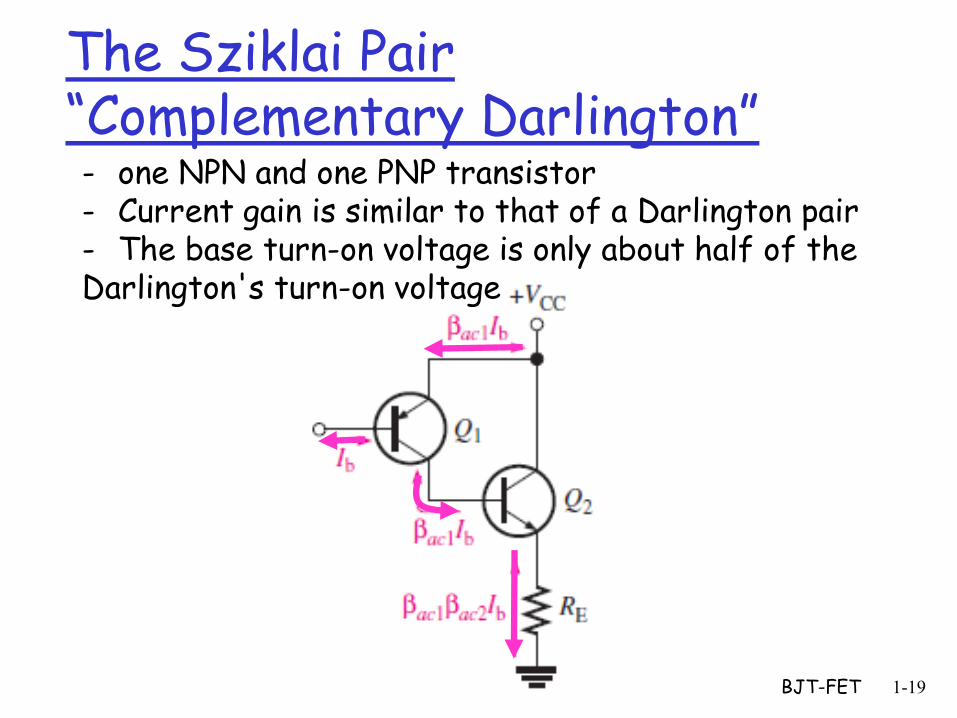
The Sziklai Pair “Complementary Darlington”
BJT-FET 1-19
- one NPN and one PNP transistor - Current gain is similar to that of a Darlington pair - The base turn-on voltage is only about half of the Darlington's turn-on voltage
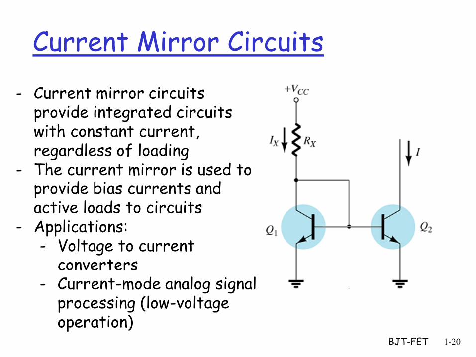
Current Mirror Circuits
BJT-FET 1-20
- Current mirror circuits provide integrated circuits with constant current, regardless of loading
- The current mirror is used to provide bias currents and active loads to circuits
- Applications: - Voltage to current
converters - Current-mode analog signal
processing (low-voltage operation)
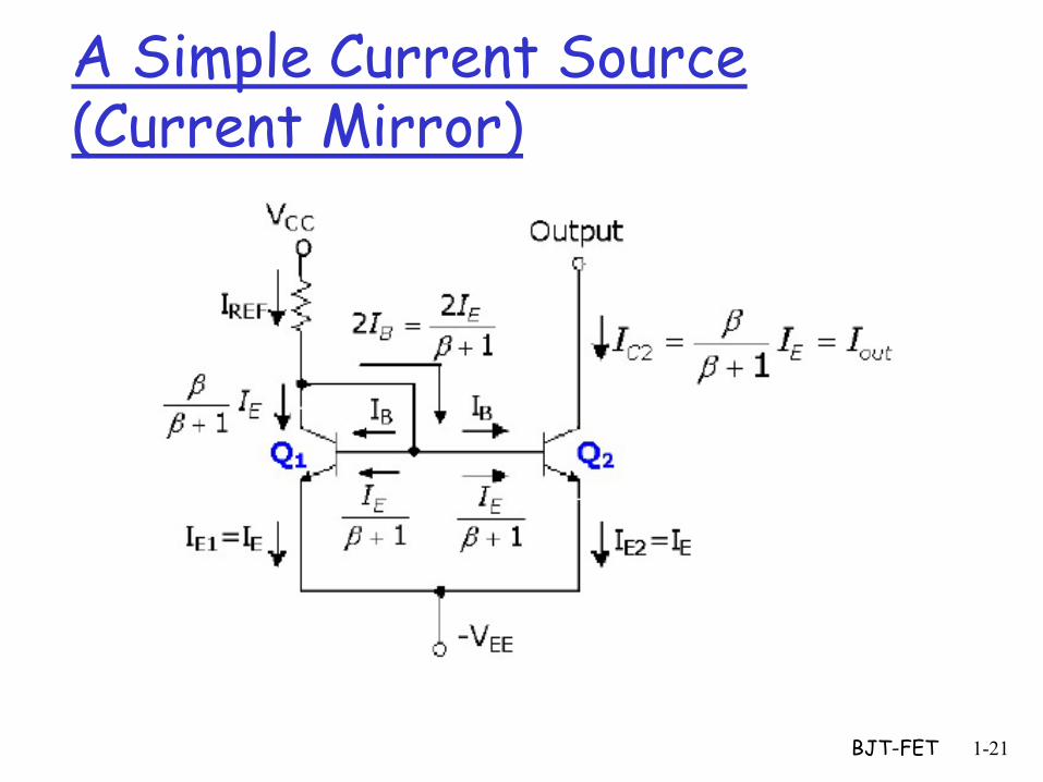
A Simple Current Source (Current Mirror)
BJT-FET 1-21
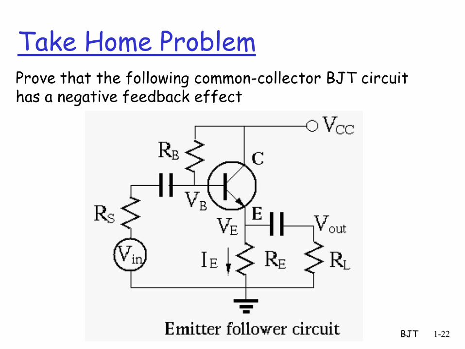
Take Home Problem Prove that the following common-collector BJT circuit has a negative feedback effect
BJT 1-22
BJT-FET 1-23
Lecture Summary
Covered material Introduction to cascaded systems using BJT Introduction to BJT-FET Combination Circuits
Combination of BJT and FET device in a circuit


![[DSE] 0 Polarizacion de transistores BJT y FET](https://static.fdocuments.net/doc/165x107/5464d3e8af795969338b4b6b/dse-0-polarizacion-de-transistores-bjt-y-fet.jpg)