Lecture 15 Sequential Circuit Design
26
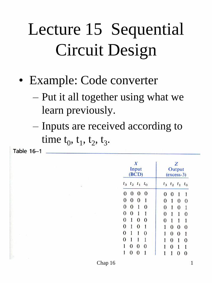
Chap 16 1 Lecture 15 Sequential Circuit Design • Example: Code converter – Put it all together using what we learn previously. – Inputs are received according to time t 0 , t 1 , t 2 , t 3 .
Transcript of Lecture 15 Sequential Circuit Design
Chap 16 1
Lecture 15 Sequential
Circuit Design
• Example: Code converter
– Put it all together using what we
learn previously.
– Inputs are received according to
time t0, t1, t2, t3.
Chap 16 2
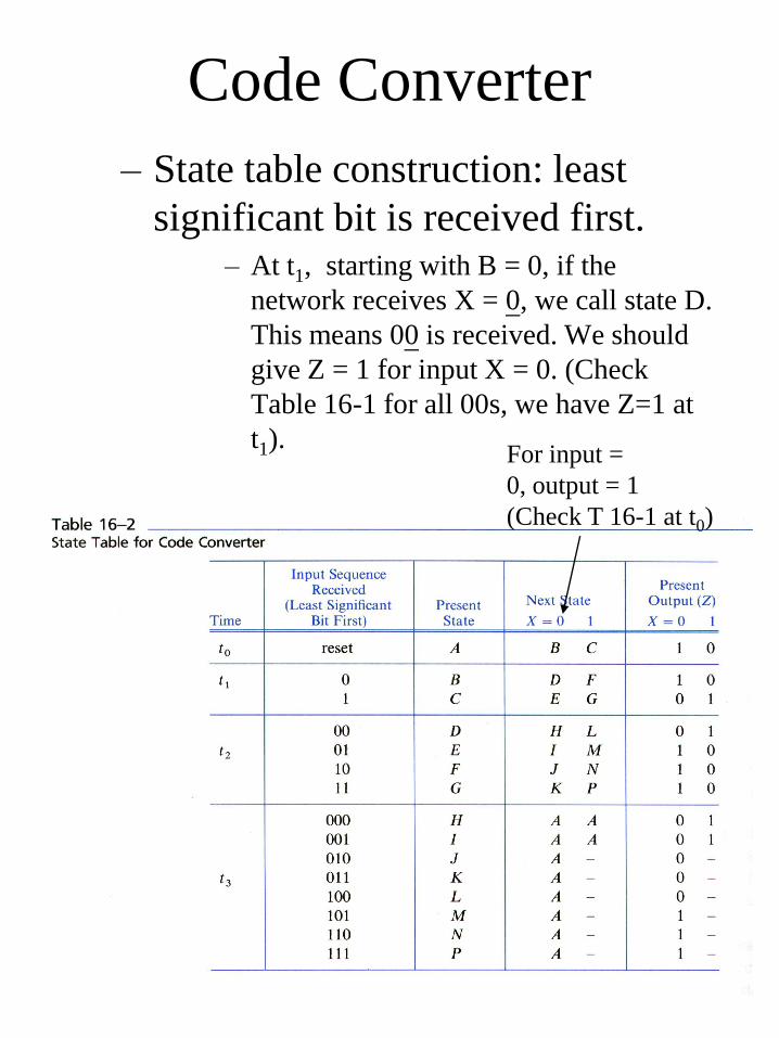
Code Converter
– State table construction: least
significant bit is received first. – At t1, starting with B = 0, if the
network receives X = 0, we call state D.
This means 00 is received. We should
give Z = 1 for input X = 0. (Check
Table 16-1 for all 00s, we have Z=1 at
t1). For input =
0, output = 1
(Check T 16-1 at t0)
Chap 16 3
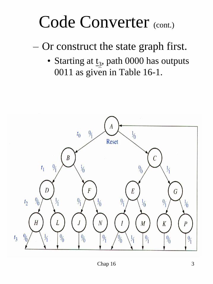
Code Converter (cont.)
– Or construct the state graph first.
• Starting at t3, path 0000 has outputs
0011 as given in Table 16-1.
Chap 16 4
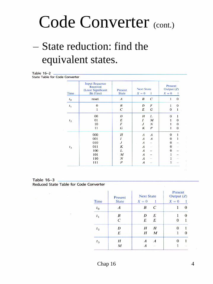
Code Converter (cont.)
– State reduction: find the
equivalent states.
Chap 16 5
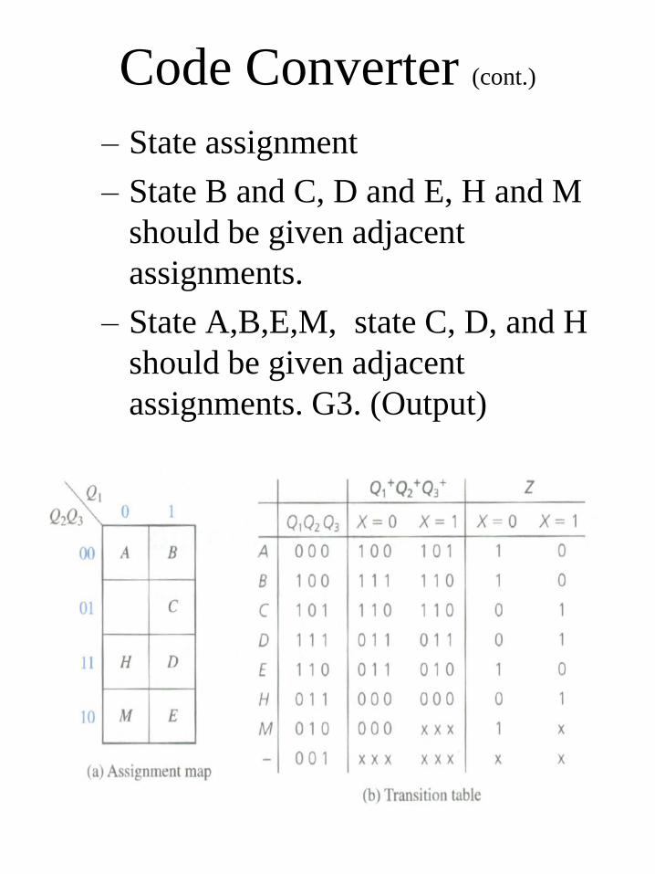
Code Converter (cont.)
– State assignment
– State B and C, D and E, H and M
should be given adjacent
assignments.
– State A,B,E,M, state C, D, and H
should be given adjacent
assignments. G3. (Output)
Chap 16 6
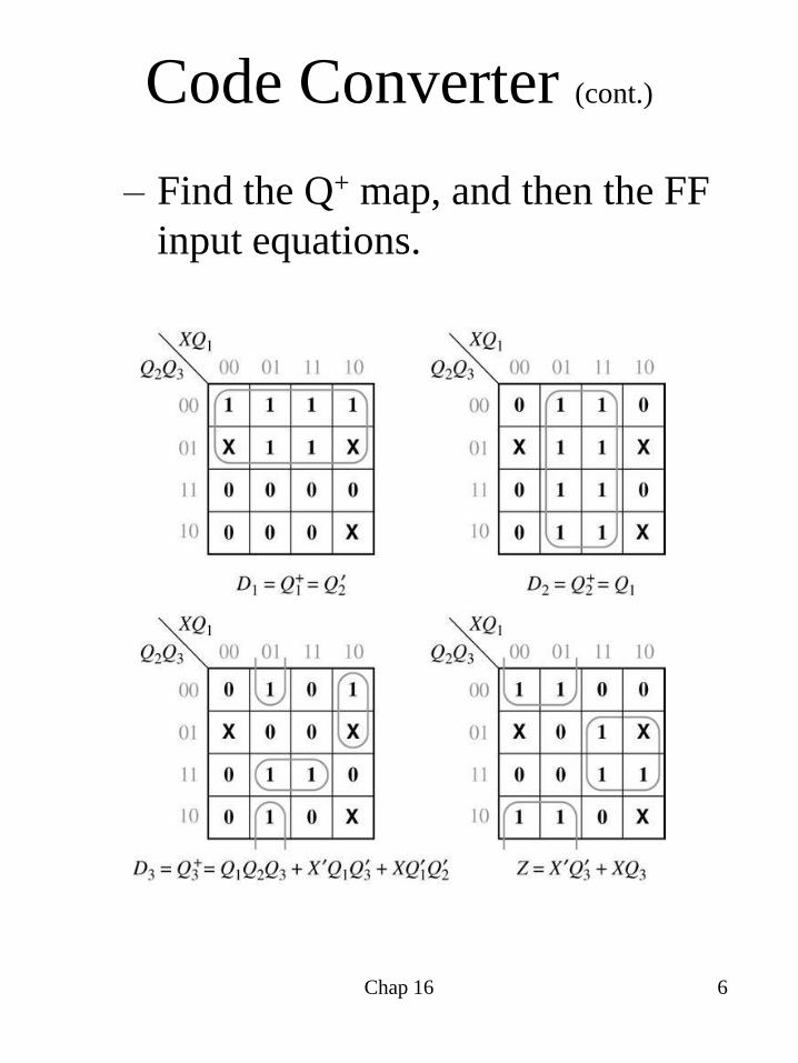
Code Converter (cont.)
– Find the Q+ map, and then the FF
input equations.
Chap 16 7
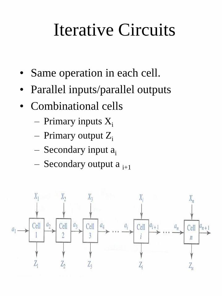
Iterative Circuits
• Same operation in each cell.
• Parallel inputs/parallel outputs
• Combinational cells
– Primary inputs Xi
– Primary output Zi
– Secondary input ai
– Secondary output a i+1
Chap 16 8
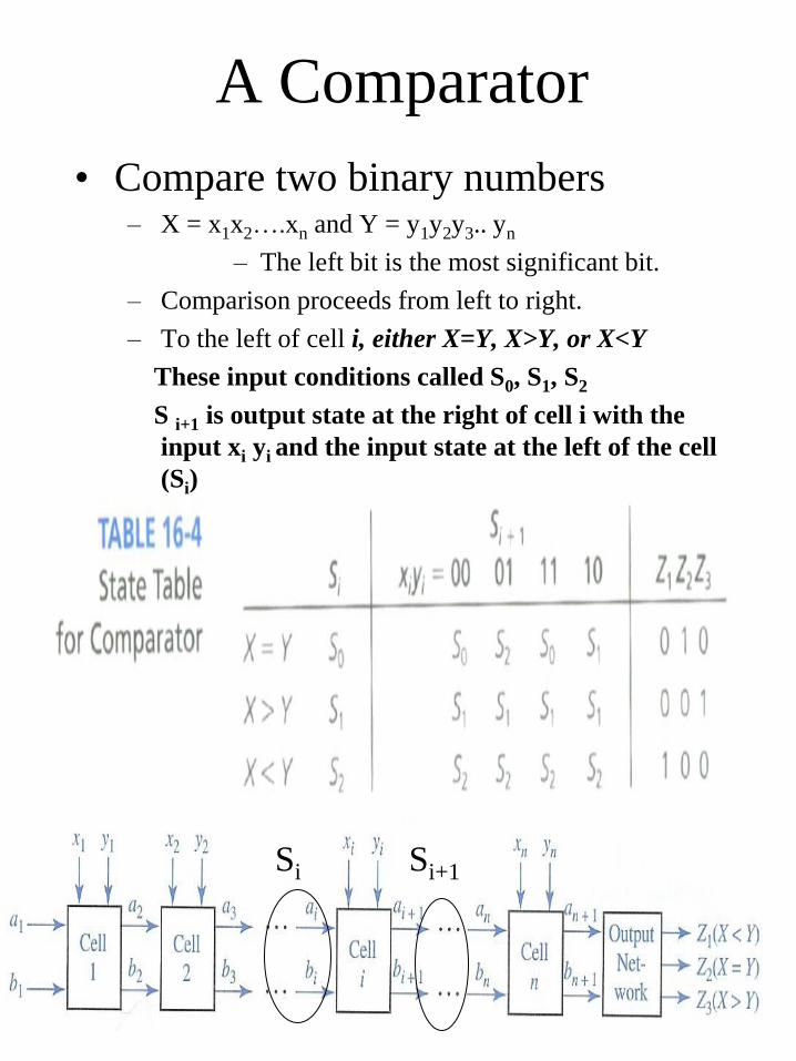
A Comparator
• Compare two binary numbers – X = x1x2….xn and Y = y1y2y3.. yn
– The left bit is the most significant bit.
– Comparison proceeds from left to right.
– To the left of cell i, either X=Y, X>Y, or X<Y
These input conditions called S0, S1, S2
S i+1 is output state at the right of cell i with the
input xi yi and the input state at the left of the cell
(Si)
Si Si+1
Chap 16 9
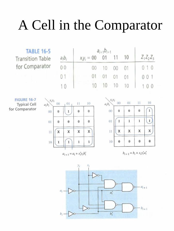
A Cell in the Comparator
• State
assignment
Chap 16 10
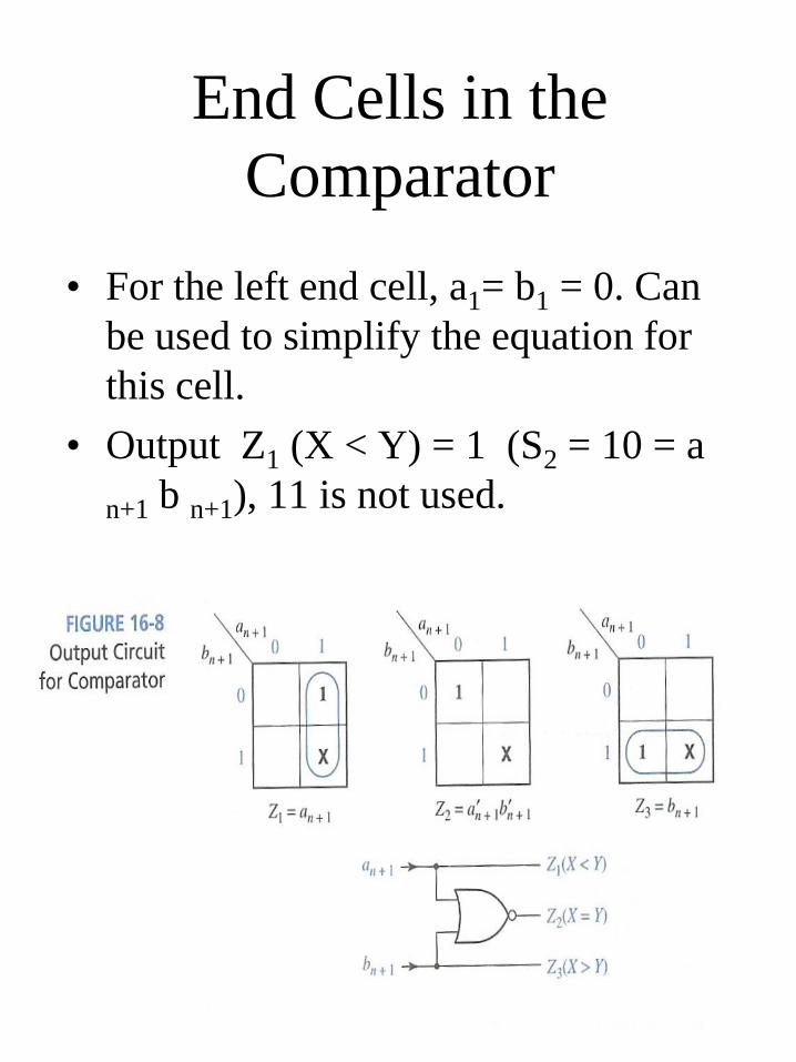
End Cells in the
Comparator
• For the left end cell, a1= b1 = 0. Can
be used to simplify the equation for
this cell.
• Output Z1 (X < Y) = 1 (S2 = 10 = a
n+1 b n+1), 11 is not used.
Chap 16 11
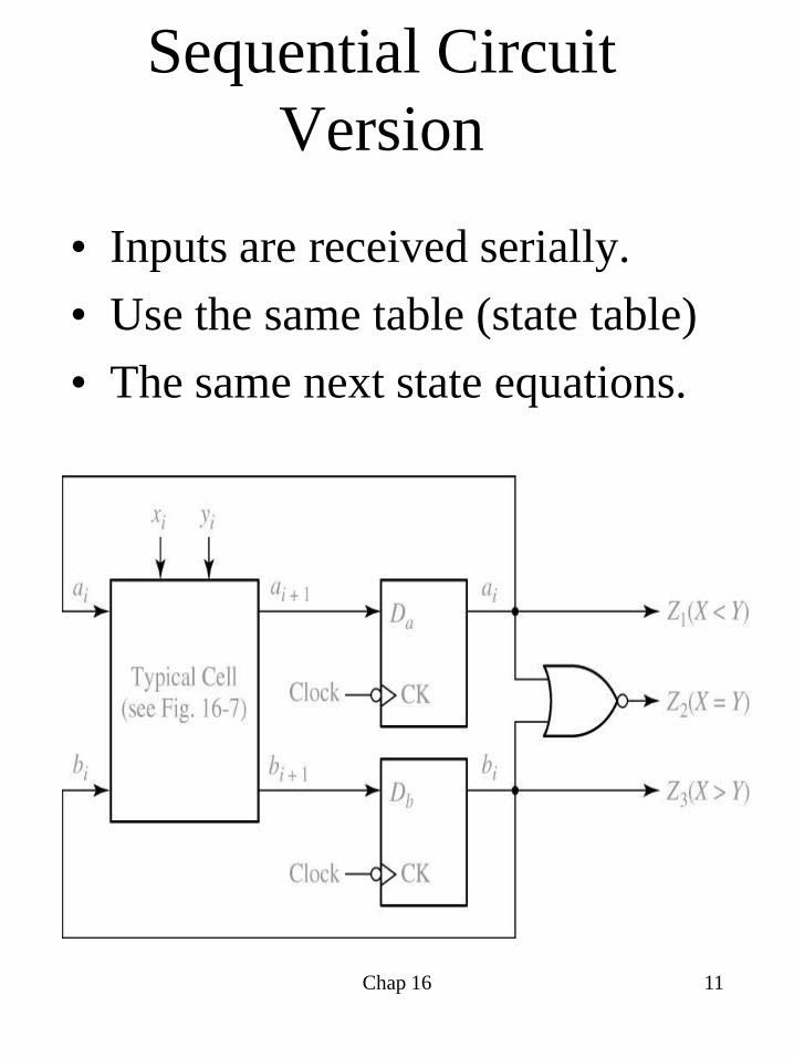
Sequential Circuit
Version
• Inputs are received serially.
• Use the same table (state table)
• The same next state equations.
Chap 16 12
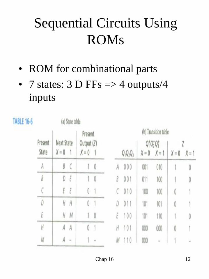
Sequential Circuits Using
ROMs
• ROM for combinational parts
• 7 states: 3 D FFs => 4 outputs/4
inputs
Chap 16 13
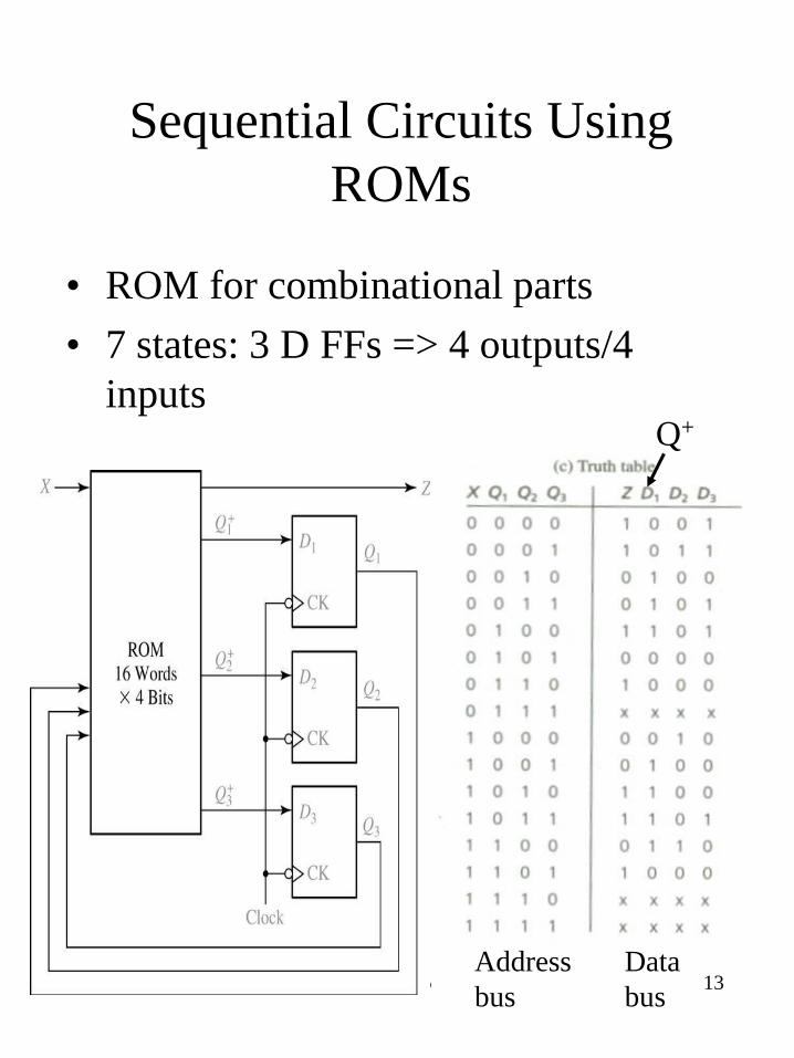
Sequential Circuits Using
ROMs
• ROM for combinational parts
• 7 states: 3 D FFs => 4 outputs/4
inputs
Address
bus
Data
bus
Q+
Chap 16 14
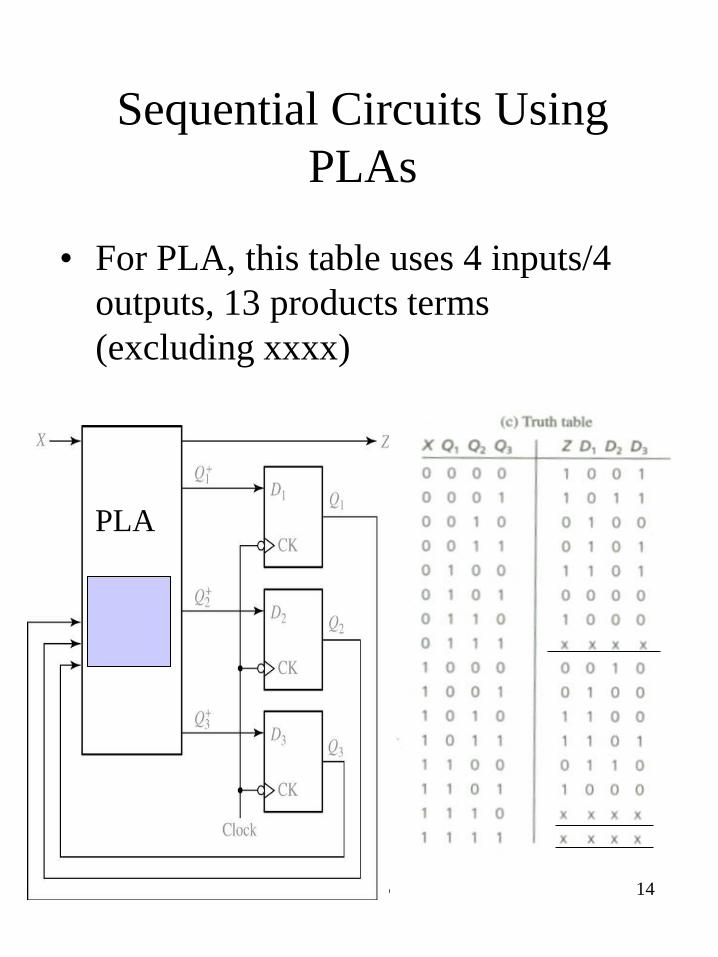
Sequential Circuits Using
PLAs
• For PLA, this table uses 4 inputs/4
outputs, 13 products terms
(excluding xxxx)
PLA
Chap 16 15
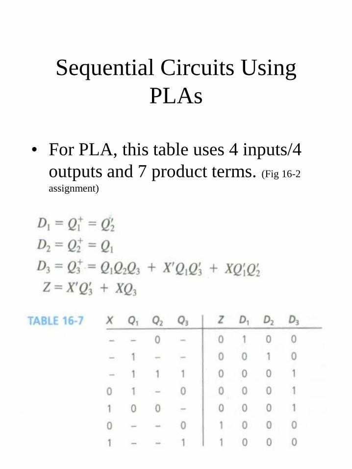
Sequential Circuits Using
PLAs
• For PLA, this table uses 4 inputs/4
outputs and 7 product terms. (Fig 16-2
assignment)
Chap 16 16
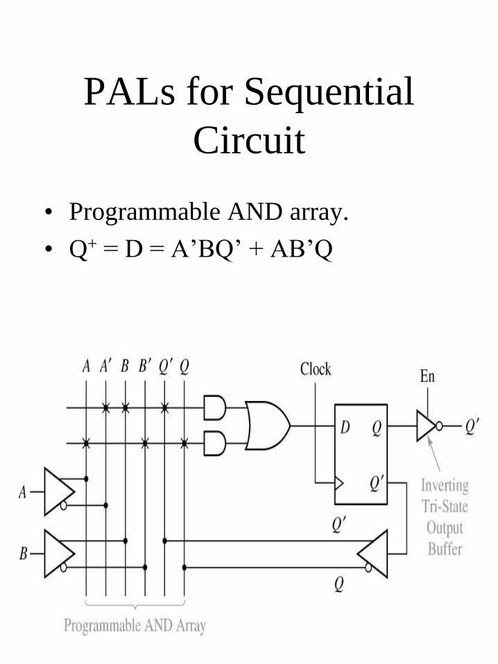
PALs for Sequential
Circuit
• Programmable AND array.
• Q+ = D = A’BQ’ + AB’Q
Chap 16 17
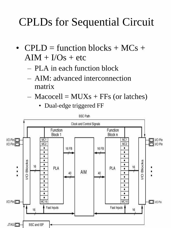
CPLDs for Sequential Circuit
• CPLD = function blocks + MCs + AIM + I/Os + etc
– PLA in each function block
– AIM: advanced interconnection matrix
– Macocell = MUXs + FFs (or latches)
• Dual-edge triggered FF
Chap 16 18
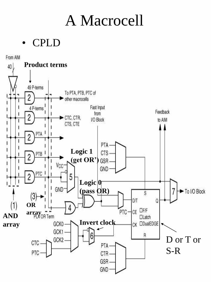
A Macrocell
• CPLD
AND
array
Product terms
OR
array
Logic 1
(get OR’)
Logic 0
(pass OR)
D or T or
S-R
Invert clock
Chap 16 19
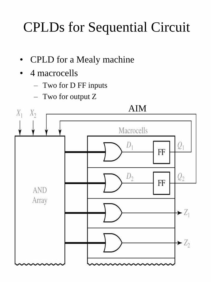
CPLDs for Sequential Circuit
• CPLD for a Mealy machine
• 4 macrocells
– Two for D FF inputs
– Two for output Z
AIM
Chap 16 20
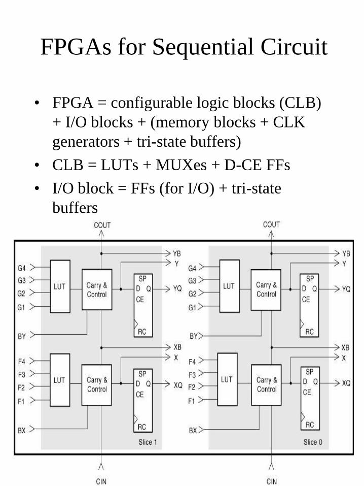
FPGAs for Sequential Circuit
• FPGA = configurable logic blocks (CLB)
+ I/O blocks + (memory blocks + CLK
generators + tri-state buffers)
• CLB = LUTs + MUXes + D-CE FFs
• I/O block = FFs (for I/O) + tri-state
buffers
Chap 16 21
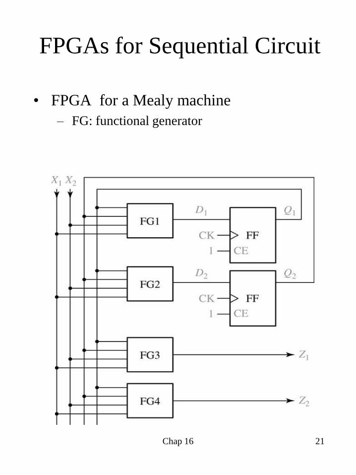
FPGAs for Sequential Circuit
• FPGA for a Mealy machine
– FG: functional generator
Chap 16 22
Simulations
• Functional level
– Sequence of transfers btw registers,
ALU, memories.
– Verify high level system design
• Logic level
– Logic gates, FF, and interconnection
– Verify logic design and analyze timing
• Circuit level
– Each gate is represented in transistors,
R, C.
– Information about voltage level and
switching speed.
Chap 16 23
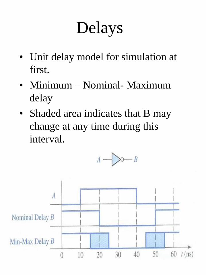
Delays
• Unit delay model for simulation at
first.
• Minimum – Nominal- Maximum
delay
• Shaded area indicates that B may
change at any time during this
interval.
Chap 16 24
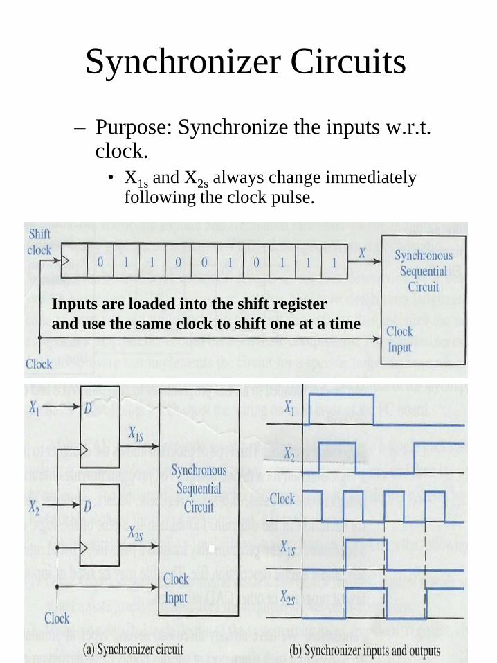
Synchronizer Circuits
– Purpose: Synchronize the inputs w.r.t. clock.
• X1s and X2s always change immediately following the clock pulse.
Inputs are loaded into the shift register
and use the same clock to shift one at a time
Chap 16 25
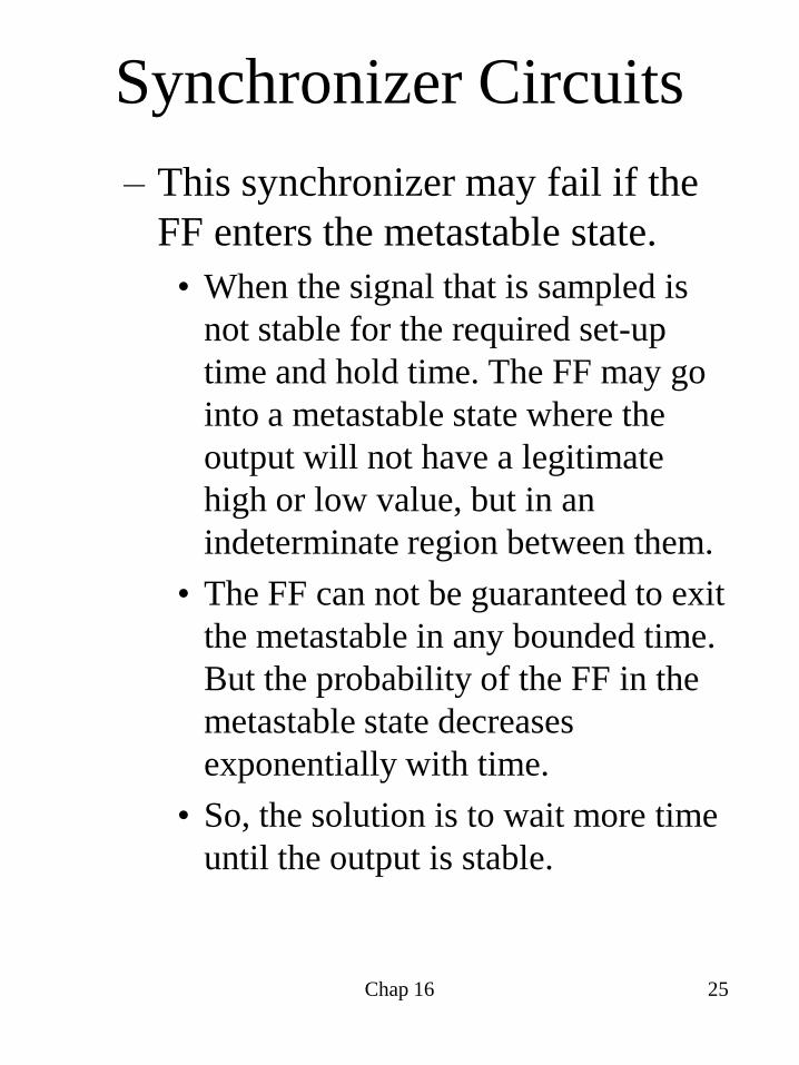
Synchronizer Circuits
– This synchronizer may fail if the
FF enters the metastable state.
• When the signal that is sampled is
not stable for the required set-up
time and hold time. The FF may go
into a metastable state where the
output will not have a legitimate
high or low value, but in an
indeterminate region between them.
• The FF can not be guaranteed to exit
the metastable in any bounded time.
But the probability of the FF in the
metastable state decreases
exponentially with time.
• So, the solution is to wait more time
until the output is stable.
Chap 16 26
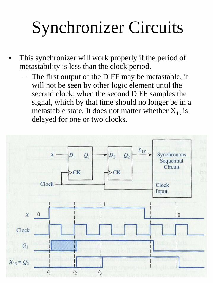
Synchronizer Circuits
• This synchronizer will work properly if the period of metastability is less than the clock period.
– The first output of the D FF may be metastable, it will not be seen by other logic element until the second clock, when the second D FF samples the signal, which by that time should no longer be in a metastable state. It does not matter whether X1s is delayed for one or two clocks.