Electro – optic – Magneto Optic and Acousto – Optic effects (1)
Upload
bruno-garcia-tejadaCategory
view
65download
4description

Fiber Optic CommunicationFiber Optic CommunicationSemiconductor Laser
Lecture 12Lecture 12
Khosrow GhadiriElectrical Engineering Department Electrical Engineering Department
San Jose State University

Principle of LASER diodeLASER is an acronym for Light Amplification by Stimulated EmissionLASER is an acronym for Light Amplification by Stimulated Emissionof Radiation.Laser diodes are, like LEDs, direct bandgap pn-junction used underforward bias.Laser diodes are devices emitting coherent light produced in thestimulated emission process whereas LEDs under injectionexcitement emit light produced in spontaneous emission process.Laser lasing wavelength ranges from the visible to the infraredLaser lasing wavelength ranges from the visible to the infraredwavelength depending on the material of the active layer.In the 850 nm-band AlGaAs/GaAs and in the 1300/1550 nm-bandsInGaAsP/InP material system are commonly used in fiber opticcommunication. AlGaAs/AlGaAs, and group-III nitride are used inthe visible wavelength.Laser diodes composed of III-V compound semiconductor and aswell as some II-VI compound are used in visible wavelength.
© Khosrow Ghadiri Fiber Optics Communications EE Dept. SJSU
2
well as some II VI compound are used in visible wavelength.

HistoryThe first semiconductor laser were reported by R N Hall et al fromThe first semiconductor laser were reported by R.N. Hall et al. fromGeneral Electric research laboratory and Marshal I. Nathan et al.from IBM, Thomas J. Watson Research Center based on GaAs pnjunction in 1962.
( ) l h dContinuous-wave (CW) lasing at room temperature was achieved inan AlGaAs/GaAs double-heterostructure laser in 1970.I. Hayashi et al. Junction lasers which operates continuously at roomtemperature, Appl. Phys. Lett., 17, 109, 1970.temperature, Appl. Phys. Lett., 17, 109, 1970.Zh. I. Alferov, et al. Investigation of the influence of the AlAs-GaAsheterostructure parameters on the laser threshold current and therealization of continuous emission at room temperature, Sov. Phys,S i d 4 1573 1971Semicond. 4, 1573, 1971.
© Khosrow Ghadiri Fiber Optics Communications EE Dept. SJSU
3

Laser safetyLaser safetyLaser safety
© Khosrow Ghadiri Fiber Optics Communications EE Dept. SJSU
4

Laser safety ANSI standardsAmerican National Standard Institute Laser safety classification:American National Standard Institute Laser safety classification:Class 1:
Inherently safe.No viewing hazard during normal use or maintenanceNo control or label requirements (typically 0 4 microwatts or lessNo control or label requirements (typically 0.4 microwatts or lessoutput power)
Class 1M:Inherently safe if not view through collecting optics.Designed to allow for arrays of optical sources which may beDesigned to allow for arrays of optical sources which may beviewed at the same time.
Class 2:Normal human eye blink response or aversion response issufficient to protect the user.sufficient to protect the user.Low power visible laser (<1 mW continuous operation).In pulsed operation, waning labels are required if power levelsexceed the class 1 acceptable exposure duration, but do notexceed class 1 limits for a 0.25 second exposure.
© Khosrow Ghadiri Fiber Optics Communications EE Dept. SJSU
5
p

Laser safety ANSI standardsAmerican National Standard Institute Laser safety classification:American National Standard Institute Laser safety classification:Class 2A:
Warning labels are required.Low power visible laser that do not exceed class 1 acceptablelimits for 1000 seconds or less and system which are notlimits for 1000 seconds or less and system which are notdesigned for intentional viewing of the beam.
Class 3A:Normal human eye blink response or aversion response issufficient to protect the user, unless laser is viewed throughp , gcollecting optics.Requires warning labels, enclosure/interlocks on the system,and warning signs at room entrance where the laser is housed.Typically 1-5 mW power.
Class 3B:Direct viewing is hazard, and specular reflections may pose ahazard.Same warning label requirements as class 3A plus power
t t d i li ht h l i i ti
© Khosrow Ghadiri Fiber Optics Communications EE Dept. SJSU
6
actuated warning light when laser is in operation.

Laser safety ANSI standardsAmerican National Standard Institute Laser safety classification:American National Standard Institute Laser safety classification:Class 3B: continuation
Typically 5-500 mW continuous output power, <10 joules persquare centimeter pulsed operation for <0.25second.
Class 4:Class 4:Direct viewing is hazard, and specular or diffuse reflections maypose a hazard.Skin protection and fire protection are concerns.Same warning label requirements as class 3B plus a locked door,Same warning label requirements as class 3B plus a locked door,door actuated power kill switch or door actuated optical filter,Shutter, or equivalent.Typically >500 mW continuous output power, >10 joules persquare centimeter pulsed operation.
© Khosrow Ghadiri Fiber Optics Communications EE Dept. SJSU
7

Safety goggleSafety goggle is categorized by wavelength and maximum powerSafety goggle is categorized by wavelength and maximum power
© Khosrow Ghadiri Fiber Optics Communications EE Dept. SJSU
8

Periodic table of elements.
© Khosrow Ghadiri Fiber Optics Communications EE Dept. SJSU
9

Simplified orbital model of many electron atoms
Bohr’s modelBohr s model
© Khosrow Ghadiri Fiber Optics Communications EE Dept. SJSU
10

Carrier concentration and bandgapBandgap width 2Bandgap width
Intrinsic carrier concentration
2
g goTE E
Tαβ
= ++
3 2 2gE
kTi ion n T e−=
( ) 15 37 3 10n Si cm−= ×( ) 7.3 10ion Si cm= ×
Semiconductor
Germanium 0.7437 0.66 235
@ 0 ( )gE K eV @300 ( )gE K eV ( / )eV Kα ( )Kβ44 .7 7 4 1 0 −×
Silicon 1.170 1.12 636
GaAs 1.519 1.42 204
44.73 10−×
45.405 10 −×
© Khosrow Ghadiri Fiber Optics Communications EE Dept. SJSU
11

Comparison of Three Statistical Distributionr Maxwell- Bose-Einstein Fermi-DiracMaxwell
BoltzmannBose Einstein Fermi Dirac
Particle system Identical but distinguishable particles
Identical indistinguishable particles with integer
Identical indistinguishable particles with half-integer spin
particles particles with integer spin
Particles Classical Bosons Fermions
Examples Ideal gas at thermal equilibrium
Photons in a cavity.Photons in a solid
Electrons in a metal. Conduction in semiconductors. thermal equilibrium Photons in a solid semiconductors.
Distribution function F(ε) = (Aeε/kT) -1 F(ε) = ( Aeε/kT -1) -1 F(ε) = ( Aeε/kT +1) -1
Obeying Pauli Exclusion principal No No Yes
Properties of distribution
No limit to how many particles can occupy a given
No limit to how many particles can occupy a given quantum state
Never be more than one particle in
any quantum state
© Khosrow Ghadiri Fiber Optics Communications EE Dept. SJSU
12
occupy a given quantum state
given quantum state any quantum state

LaserGas die and semiconductor lasersGas, die, and semiconductor lasers
© Khosrow Ghadiri Fiber Optics Communications EE Dept. SJSU
13

Laser wavelength Laser wavelength range in visible and infrared regionsLaser wavelength range in visible and infrared regions
Loss
0.85μ 1.30μ 1.55μdB
Loss
( )
© Khosrow Ghadiri Fiber Optics Communications EE Dept. SJSU
14
( )mλ μ

LaserPhoton energy:Photon energy:
The radiated wavelength:photon gE E hf= =
1.24hcλ
The optic power output when gap energy is in joule:g gE E
λ = =
gEP NE i
ηη
Where N is the number of charge per second:
ggP NE i
qη= =
iN =
The optic power output when gap energy is in eV:
Nq
=
P iEη=
© Khosrow Ghadiri Fiber Optics Communications EE Dept. SJSU
15
gP iEη

Bandgap engineeringTernary alloys: for example GaAs laser doped with Al cover theTernary alloys: for example GaAs laser doped with Al cover thewavelength range from 850 nm to 780 nm with increasing x
AlX Ga 1-X As
Cd Mn TeCd 1-X MnXTe
GaAS 1-X PX
GaXIn 1-X As
Quaternary alloys: GaAs doped with In and P cover the wavelengthrange from 900 nm to 1670 nm with increasing x and y
X 1-X
Hg 1-X CdXTe
range from 900 nm to 1670 nm with increasing x and yGaX In1-X As1-Y PY
AlX Ga1-X AsY Sb1-Y
© Khosrow Ghadiri Fiber Optics Communications EE Dept. SJSU
16
X 1 X Y 1 Y

Laser power rangeLaser power ranges:Laser power ranges:Continuous wave power:
~1 mW for communications, data storage, laser pointersto ~100kW for machiningto 100kW for machiningto ~5MW for military
Pulsed power:to ~ W1510
Pulse length as short as ~5 fsecCavity length ~1 for VCSEL to 6.5 kmmμ
© Khosrow Ghadiri Fiber Optics Communications EE Dept. SJSU
17

Principle of laser diodeSemiconductor laser commonly used in fiber optic Semiconductor laser commonly used in fiber optic communication because:
Long lifeHigh reliabilityHigh reliabilityRuggednessCompactnessLight weightLight weightHigh efficiency of electrooptric conversionLow applied voltageSpectral purity compared to non laser sourceSpectral purity compared to non laser source.Direct modulation capability up to tens of gigahertz.
© Khosrow Ghadiri Fiber Optics Communications EE Dept. SJSU
18

The gas laserThe gas laserThe gas laser
© Khosrow Ghadiri Fiber Optics Communications EE Dept. SJSU
19

The gas laserThe gas laserThe gas laser
© Khosrow Ghadiri Fiber Optics Communications EE Dept. SJSU
20

Laser bench Laser benchLaser bench
© Khosrow Ghadiri Fiber Optics Communications EE Dept. SJSU
21

Laser diodesLaser diodesLaser diodes
© Khosrow Ghadiri Fiber Optics Communications EE Dept. SJSU
22

Principle of LASER diodeIn degenerately doped pn junction The Fermi levelIn degenerately doped pn junction, The Fermi level
© Khosrow Ghadiri Fiber Optics Communications EE Dept. SJSU
23

pn Junction diode
W
p n p n
FV
p n
RV−
p n
+ − + −
E E EE
cpE
FpE cnE0qV( )0 Fq V V−
( )0 Rq V V+
cpE
FpEE
cnEFnE
cpE
E cnEE
cpE
EFp
vpE FnE
vnE
( )0 Rq V V+
V( )0 FV V−
vpEvnE FVFpE
vpE FnE
vnE cnEFnE
vnE
FpEvpE
RV
0V
pV
nV
( )0 RV V+
Equilibrium Forward biasedBefore Contact Reverse biased
© Khosrow Ghadiri Fiber Optics Communications EE Dept. SJSU
24
Equilibrium Forward biasedBefore Contact Reverse biased

Degenerate pn Junction diode
W
p n p n
FV+ −
W
p+ n+ p+ n+
FV+ −
E E
cpE
FE cnE0qV( )0 Fq V V−
cpE
E cnEE
E E
cpE
EvpE
E0qV
( )0 Fq V V−cpE
E cnEE
++++−−−−
FpEvpE
cn
FnE
vnE
V( )0 FV V−
FVFpEvpE FnE
vnE
FpEcnEFnE
vnE
V( )0 FV V−
FVFpEvpE FnE
vnE
−−−−++++
VV
0V
pV
nV
Equilibrium Forward biased
0V
pV
nV
Equilibrium Forward biased
nV
pVnV
pV
© Khosrow Ghadiri Fiber Optics Communications EE Dept. SJSU
25
Equilibrium Forward biased Equilibrium Forward biased

Degenerately doped pn junctionIn degenerately doped pn junction The Fermi level in the p-sideEIn degenerately doped pn junction, The Fermi level in the p sideis in the valence band and that in the n-side is in the conductionband.All the energy levels up to The degenerately direct bandgap
d h h b d d
fpEfnE
semiconductor pn junction such as GaAs has band diagram:
hf −FreeElectron
Conduction Band
V
si
i
outV ElectronE
hf
hf 8W
hf ElectronCreated
+ +
FV+ −
DCI
Energyhf +FreeHoleCreated
JunctionValence Band
p+ n+
E
© Khosrow Ghadiri Fiber Optics Communications EE Dept. SJSU
26

Digital modulation of laser diodeIn the forward biased p-n junction laser diode The potentialIn the forward biased p n junction laser diode, The potentialenergy barrier between the p and n regions decreases , so electronand hole flow, hence current flow.
Incident photon after passing through p-region will be absorbed in the depletion layer.
© Khosrow Ghadiri Fiber Optics Communications EE Dept. SJSU
27

InGaAsP laser diode structureInGaAsP laser diode structureInGaAsP laser diode structure.
© Khosrow Ghadiri Fiber Optics Communications EE Dept. SJSU
28

LED and LDCurrent flow in LED and LD Current flow in LED and LD
Light power Laser diode 3030 0.30 15
A)Plaser mode
LEDmode
25 1300C nm°
)Ω
LED
5 mW
10 mW
2020G
E, V
(V)
ower
, P (m
W)
0.20 10
/ fac
et, d
P/d
l (W
/A
sist
ance
, dV/
dl
V
P
/ ( )s stdP dl η −=
(Ω
Current0
100 mA50 mA
1010VO
LTA
G
Ligh
t out
put p
o
0.10 5
Slo
pe e
ffeci
ency
Diff
eren
tial r
es
/ ( )dV dl Rs=
ypical optical power output vs. forward currentr a LED and a laser diode.999 S.O. Kasap, Optoelectronics (Prentice Hall)
C t l ( A)
00 0 050 100 1500
threshold current
© Khosrow Ghadiri Fiber Optics Communications EE Dept. SJSU
29
999 S.O. s p, Optoelect onics ( e ce )Current, l (mA)

RecombinationRecombination is the electron transition from the conduction bandRecombination is the electron transition from the conduction bandto fill a hole in the valence band.Recombination can be viewed as the annihilation of a negativecarrier (conduction electron) and a positive carrier (hole in thevalence band) and energy is released either as radiated photon orvalence band), and energy is released either as radiated photon orphonon (heat in the lattice of crystal).The electron density which is the number of electrons per unitvolume in energy levels between and in the conductionband is given by:
( )2n E2E 2 2E dE+
band, is given by:
where the is the density of states per unit energy per unitl i th d ti b d t l l
( ) ( ) ( )2 2 2 2 2c cn E dE g E f E dE=
( )2cg EEvolume in the conduction band at energy level
is the effective mass of electron
( )*3 2
2 23 2
2 ec c
mg E E Eπ
= −
2E
*m
© Khosrow Ghadiri Fiber Optics Communications EE Dept. SJSU
30
is the effective mass of electronem

Fermi-Dirac distributionThe Fermi-Dirac distribution function specifies the probability( )2f EThe Fermi Dirac distribution function specifies the probabilitythat the energy level in the conduction band is occupied by anelectron.
2E( )2cf E
( ) ( )22
1fn
c E Ef E
−=
1kTe +
The is the quasi-Fermi level of electrons in the conduction bandand is the bottom edge of the conduction band.E
fE
© Khosrow Ghadiri Fiber Optics Communications EE Dept. SJSU
31
and is the bottom edge of the conduction band.cE

Hole densitySimilarly the hole density which is the number of holes per unit( )1p ESimilarly the hole density which is the number of holes per unitvolume in energy levels between and in the conductionband, is given by:
( ) ( ) ( )1 1 1 1 11p E dE g E f E dE= −⎡ ⎤⎣ ⎦
( )1p E1E 1 1E dE+
where the is the density of states per unit energy per unitvolume in the conduction band at energy level
( ) ( ) ( )1 1 1 1 11v vp E dE g E f E dE⎡ ⎤⎣ ⎦
*3 22
( )1vg E1E
is the effective mass of holeThe Fermi-Dirac distribution function specifies the probability
( )*3 2
1 13 2
2 hc v
mg E E Eπ
= −*hm
( )f EThe Fermi-Dirac distribution function specifies the probabilitythat the energy level in the valence band is occupied by anelectron
1E( )1vf E
( ) ( )11
1fp
v E Ef E
−=
© Khosrow Ghadiri Fiber Optics Communications EE Dept. SJSU
32
1kTe +

Hole densityThe probability of the absence of electron or the presence of theThe probability of the absence of electron or the presence of thehole at in the valence band1E 1 1E dE+
( ) ( )11
11 1fp
v E Ef E
−− = −
The potential energy of bias voltage is:FeV
eV E E= −
1kTe +
FV
Gain is the difference between stimulated emission and absorption.Stimulated emission in semiconductor occurs when an incidenth t i d l t t k th t iti f d ti
F fn fpeV E E=
photon induces an electron to make the transition from conductionband to the valence band and is proportional to productwhich is the density of electrons in the conduction band and thedensity of holes in the valence band.
© Khosrow Ghadiri Fiber Optics Communications EE Dept. SJSU
33
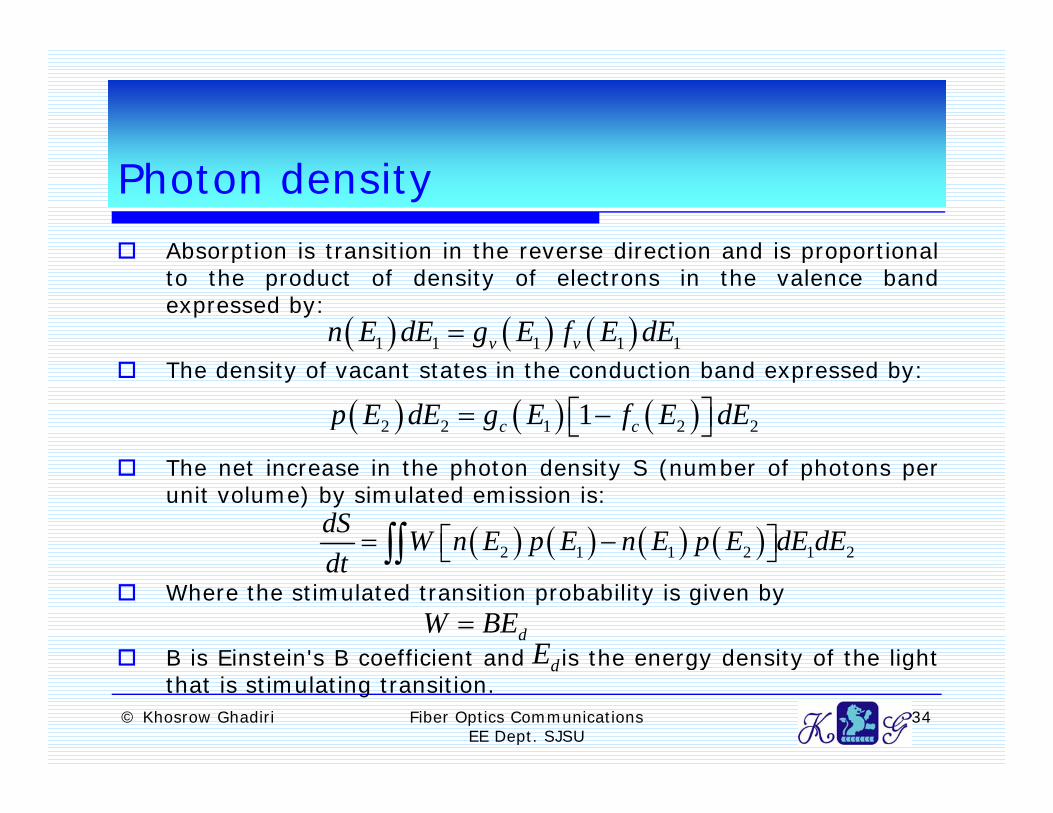
Photon densityAbsorption is transition in the reverse direction and is proportionalAbsorption is transition in the reverse direction and is proportionalto the product of density of electrons in the valence bandexpressed by:
( ) ( ) ( )1 1 1 1 1v vn E dE g E f E dE=The density of vacant states in the conduction band expressed by:
( ) ( ) ( )2 2 1 2 21c cp E dE g E f E dE= −⎡ ⎤⎣ ⎦The net increase in the photon density S (number of photons perunit volume) by simulated emission is:
( ) ( ) ( ) ( )2 1 1 2 1 2dS W n E p E n E p E dE dEdt
= −⎡ ⎤⎣ ⎦∫∫Where the stimulated transition probability is given by
B is Einstein's B coefficient and is the energy density of the light
dt ⎣ ⎦∫∫
dW BE=dE
© Khosrow Ghadiri Fiber Optics Communications EE Dept. SJSU
34
B is Einstein s B coefficient and is the energy density of the lightthat is stimulating transition.
dE

Photon densityThe energy density of the light that simulating the transition isThe energy density of the light that simulating the transition isgiven by:
The increase in the energy density of the light is:dE hfS=
g g
is related to the light intensity by:
( ) ( ) ( ) ( )2 1 1 2 1 2d
ddE BhfE n E p E n E p E dE dEdt
= −⎡ ⎤⎣ ⎦∫∫dE SI
Where is the velocity of light:
sd
IEv
=v
( ) ( ) ( ) ( )2 1 1 2 1 2d s s
stim stim stim
dE dI dI Bhf n E p E n E p E dE dEdt vdt dz v
⎛ ⎞ ⎛ ⎞ ⎛ ⎞= = = −⎡ ⎤⎜ ⎟ ⎜ ⎟ ⎜ ⎟ ⎣ ⎦⎝ ⎠ ⎝ ⎠ ⎝ ⎠ ∫∫
© Khosrow Ghadiri Fiber Optics Communications EE Dept. SJSU
35

Light intensityThe net increase in the photon density S (number of photons perThe net increase in the photon density S (number of photons perunit volume) by spontaneous emission is:
( ) ( )2 1 1 2spon
dS An E p E dE dEdt
⎛ ⎞ =⎜ ⎟⎝ ⎠ ∫∫
A is Einstein's A coefficient.The change in light intensity variation due to spontaneous emissionis:
spon⎝ ⎠
( ) ( )dI hfA d d⎛ ⎞∫∫
The total resultant light intensity variation is
( ) ( )2 1 1 2s
spon
dI hfA n E p E dE dEdt v
⎛ ⎞ =⎜ ⎟⎝ ⎠ ∫∫
s s s
stim stim
dI dI dIdz dz dz
⎛ ⎞ ⎛ ⎞ ⎛ ⎞= +⎜ ⎟ ⎜ ⎟ ⎜ ⎟⎝ ⎠ ⎝ ⎠ ⎝ ⎠
© Khosrow Ghadiri Fiber Optics Communications EE Dept. SJSU
36

GainThe total resultant light intensity variation is:The total resultant light intensity variation is:
( ) ( )s s ss
stim stim
dI dI dI g hf I h hfdz dz dz
⎛ ⎞ ⎛ ⎞ ⎛ ⎞= + = +⎜ ⎟ ⎜ ⎟ ⎜ ⎟⎝ ⎠ ⎝ ⎠ ⎝ ⎠
Where:
( ) ( ) ( ) ( ) ( )2 1 1 2 1 2s
stim
dI hfg hf B n E p E n E p E dE dEdz v
⎛ ⎞= = −⎡ ⎤⎜ ⎟ ⎣ ⎦⎝ ⎠ ∫∫
or
stim⎝ ⎠
( ) ( ) ( )2 1 1 2s
spon
dI hfh hf A n E p E dE dEdt v
⎛ ⎞= =⎜ ⎟⎝ ⎠ ∫∫
( ) ( ) ( ) ( ) ( )2 1 2 1 1 2s
c v c vstim
dI hfg hf B g E g E f E f E dE dEdz v
⎛ ⎞= = −⎡ ⎤⎜ ⎟ ⎣ ⎦⎝ ⎠ ∫∫
© Khosrow Ghadiri Fiber Optics Communications EE Dept. SJSU
37
The condition for positive gain is obtained if 2 1fn fpE E E E− > −

Light intensityThe total resultant light intensity variation is:The total resultant light intensity variation is:
( ) ( )s s ss
stim stim
dI dI dI g hf I h hfdz dz dz
⎛ ⎞ ⎛ ⎞ ⎛ ⎞= + = +⎜ ⎟ ⎜ ⎟ ⎜ ⎟⎝ ⎠ ⎝ ⎠ ⎝ ⎠
Where:
( ) ( ) ( ) ( ) ( )2 1 1 2 1 2s
stim
dI hfg hf B n E p E n E p E dE dEdz v
⎛ ⎞= = −⎡ ⎤⎜ ⎟ ⎣ ⎦⎝ ⎠ ∫∫
or
stim⎝ ⎠
( ) ( ) ( )2 1 1 2s
spon
dI hfh hf A n E p E dE dEdt v
⎛ ⎞= =⎜ ⎟⎝ ⎠ ∫∫
( ) ( ) ( ) ( ) ( )2 1 2 1 1 2s
c v c vstim
dI hfg hf B g E g E f E f E dE dEdz v
⎛ ⎞= = −⎡ ⎤⎜ ⎟ ⎣ ⎦⎝ ⎠ ∫∫
© Khosrow Ghadiri Fiber Optics Communications EE Dept. SJSU
38
The condition for positive gain is obtained if 2 1fn fpE E E E− > −

Optical cavityOptical cavity: Optical cavity:
lP1R 2R
( )1 ( )R P iL
exp( )lP iLα−
1 2 exp( 2 )lR R P iLα−( )1 21 exp( 2 )lR R P iLα− −
( )21 exp( )lR P iLα− −
P exp( )P gL
exp(2 )lP gL
lP exp( )lP gL
exp(2 )lP gL
L
© Khosrow Ghadiri Fiber Optics Communications EE Dept. SJSU
39

Amplitude condition for laser oscillation
Power amplification with distance: Power amplification with distance:
Amplitude amplification for one round trip:
gzoP P e=
Amplitude amplification for one round trip:
( )2 22e
g Lj L
oE REα
β−
+=
is amplitude of the light before the trip. L is the length ofactive region, is the power attenuation coefficient, ispropagation constant, R is the amplitude reflection coefficients of
oEα β
p p g , pthe mirror whenTwo conditions should be met:
1 2andR R 1 2R R R=
( ) 1 1Re 1 ln and largeg L g Rα α− ≥ ⇒ ≥ +
© Khosrow Ghadiri Fiber Optics Communications EE Dept. SJSU
40
Re 1 ln and largeg RL R
α≥ ⇒ ≥ +

Analog modulation
Analog modulation: Analog modulation:
20
(mW
)
10t out
put p
ower
, P (
Time
0
Ligh
t
Current, l (mA)50 1000si
© Khosrow Ghadiri Fiber Optics Communications EE Dept. SJSU
41
Time

Digital modulationDigital modulation: Digital modulation:
20P
(mW
)
10
ight
out
put p
ower
, P
0
L
Time50 1000
Current, l (mA)
si
© Khosrow Ghadiri Fiber Optics Communications EE Dept. SJSU
42
Time

Temperature dependent of laser diode
Temperature dependent of laser diode : Temperature dependent of laser diode :
8w
er, P
(mW
)
60 C°70 C°80 C°6
2
ght o
utpu
t pow
30 C°40 C°50 C°4
0
Lig
50 2000 100 150
© Khosrow Ghadiri Fiber Optics Communications EE Dept. SJSU
43
Current, l (mA)

Edge emission laser
Asymmetric radiation from edge emitting LDAsymmetric radiation from edge emitting LD
120°Beam Intensity
30°Parallel Plane
045− °90− ° 45° 90°Beam Angle
Perpencicular Plane
© Khosrow Ghadiri Fiber Optics Communications EE Dept. SJSU
44
Beam Angle

Edge emission laser
Asymmetric radiation from edge emitting LDAsymmetric radiation from edge emitting LD
0
© Khosrow Ghadiri Fiber Optics Communications EE Dept. SJSU
45
ReferencesS O Kasap Optoelectronics and photonics principle and practiceS. O. Kasap, Optoelectronics and photonics principle and practicePearson Education, 2001.Titsuo Fukuda, Optical semiconductor devices, Wiley series inmicrowave and optical engineering, Wiley interscience, 1999.Gerd Keiser, Optical Fiber Communication, McGraw-hill, third edition2000.
© Khosrow Ghadiri Fiber Optics Communications EE Dept. SJSU
46