Lecture 10 Bipolar Junction Transistor...
18
Lecture 10 Bipolar Junction Transistor (BJT) BJT 1-1 Sunday 29/10/2017
Transcript of Lecture 10 Bipolar Junction Transistor...

Lecture 10
Bipolar Junction Transistor (BJT)
BJT 1-1 Sunday 29/10/2017

Outline
Continue BJT Biasing DC analysis
• Emitter-stabilized bias circuit • Voltage divider bias circuit • DC bias with voltage feedback circuit
Transistor Switching Networks • BJT switching time
BJT 1-2

Emitter-Stabilized Bias Circuit
Adding a resistor (RE) to the emitter circuit
The addition of the emitter resistor to the dc bias of the BJT provides improved stability the dc bias currents
and voltages remain closer to where they were set by the circuit when outside conditions (e.g., temperature) change
BJT 1-3

Emitter-Stabilized Bias Circuit
BJT 1-4
Base-Emitter Loop
From Kirchhoff’s voltage law:
0R1)I(-RI-V EBBBCC
0 RI-V-RI-V EEBEEECC
EB
BECC
EB
BECCB
RR
V-V
1)R(R
V-VI
Since IE = ( + 1)IB:
Solving for IB:
EB
BECCBC
R/R
V-VII

Emitter-Stabilized Bias Circuit
BJT 1-5
Collector-Emitter Loop
From Kirchhoff’s voltage law:
0 CC
VC
RC
I CE
V E
RE
I
Since IE IC:
)R (RI– V V ECCCCCE
Also:
EBEBRCCB
CCCCECEC
EEE
V V RI– V V
RI - V V V V
RI V

Voltage Divider Bias Circuit
Very stable bias circuit
The currents and voltages are nearly independent of any variations in
BJT 1-6

Approximate Analysis of Voltage Divider Bias Circuit
BJT 1-7
Where IB << I1 and I1 I2 :
Where RE > 10R2:
From Kirchhoff’s voltage law:
21
CC2B
RR
VRV
E
EE
R
VI
BEBE VVV
EECCCCCE RI RI V V
)R (RIV V
II
ECCCCCE
CE
Condition to be tested
Base-Emitter Loop
Collector-Emitter Loop

DC Bias with Voltage Feedback Circuit Another way to
improve the stability of a bias circuit is to add a feedback path from collector to base
In this bias circuit the Q-point is only slightly dependent on the transistor beta,
BJT 1-8
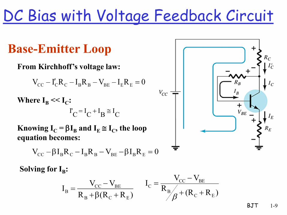
DC Bias with Voltage Feedback Circuit
BJT 1-9
Base-Emitter Loop
)R(RR
VVI
ECB
BECCB
From Kirchhoff’s voltage law:
0RI–V–RI–RI– V EEBEBBCCCC
Where IB << IC:
CI
BI
CI
CI'
Knowing IC = IB and IE IC, the loop
equation becomes:
0RIVRIRI– V EBBEBBCBCC
Solving for IB:
CC BEC
BC E
V VI
R(R R )

DC Bias with Voltage Feedback Circuit
BJT 1-10
Collector-Emitter Loop
Applying Kirchoff’s voltage law:
IERE + VCE + I’CRC – VCC = 0
Since IC IC and IE ≈ IC:
IC(RC + RE) + VCE – VCC =0
Solving for VCE:
VCE = VCC – IC(RC + RE)
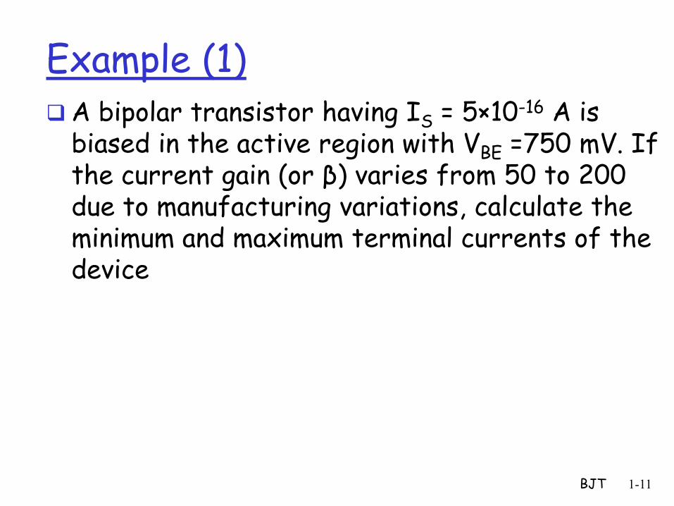
Example (1) A bipolar transistor having IS = 5×10-16 A is
biased in the active region with VBE =750 mV. If the current gain (or β) varies from 50 to 200 due to manufacturing variations, calculate the minimum and maximum terminal currents of the device
BJT 1-11

Solution For a given VBE, the collector current remains
independent of β
The base current varies from IC/200 to IC/50:
the emitter current experiences only a small variation because (β+ 1)/β is near unity for large β:
BJT 1-12
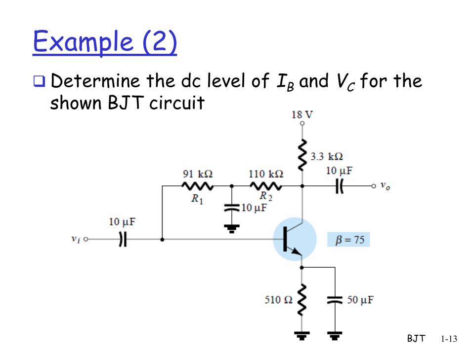
Example (2)
Determine the dc level of IB and VC for the shown BJT circuit
BJT 1-13

Solution For the dc mode,
the capacitors-related
branches become
open-circuits.
Also, RB =R1+R2
BJT 1-14

Transistor Switching Networks
Transistors with only applied DC sources at the input can be used as electronic switches
BJT 1-15
Cut-off
Saturation
Cut-off

Switching Circuit Calculations
BJT 1-16
C
CCCsat
R
VI
dc
CsatB
II
Csat
CEsatsat
I
VR
CEO
CCcutoff
I
VR
Saturation current:
To ensure saturation:
Emitter-collector resistance
at saturation and cutoff:
C
CECE
I
VR

Switching Time
BJT 1-17
Transistor switching times:
dron ttt
fsoff ttt
Times in range of nano-seconds
Example
Note: npn BJT has faster switching time than pnp BJT

BJT 1-19
Lecture Summary
Covered material Continue BJT Biasing
DC analysis • Emitter-stabilized bias circuit • Voltage divider bias circuit • DC bias with voltage feedback
Transistor Switching Networks • BJT switching time
Material to be covered next lecture
Continue BJT Continue DC analysis
• More examples
Introduction to AC signal analysis