Lect. 2: MOS Transistors (1) (Chap. 6 in Razavi)tera.yonsei.ac.kr/class/2017_1_1/lecture/Lect 2...
13
Electronic Circuits 2 (17/1) W.-Y. Choi Lect. 2: MOS Transistors (1) CMOS Inverter (Chap. 6 in Razavi)
Transcript of Lect. 2: MOS Transistors (1) (Chap. 6 in Razavi)tera.yonsei.ac.kr/class/2017_1_1/lecture/Lect 2...

Electronic Circuits 2 (17/1) W.-Y. Choi
Lect. 2: MOS Transistors (1)
CMOS Inverter
(Chap. 6 in Razavi)

Electronic Circuits 2 (17/1) W.-Y. Choi
Lect. 2: MOS Transistors (1)
NMOS
- Vertically: Metal Oxide Semiconductor
- Laterally: Source Channel Drain
(Razavi 6.2)
Capacitor
(NPN) (Initially no conduction)

Electronic Circuits 2 (17/1) W.-Y. Choi
Lect. 2: MOS Transistors (1)
Triode (VDS< VGS-VTH)
VGS > VTH
Current conduction in NMOS
21 2( )2D n ox GS TH DS DS
WI C V V V VL

Electronic Circuits 2 (17/1) W.-Y. Choi
Lect. 2: MOS Transistors (1)
Triode (VDS< VGS-VTH)
21 2( )2D n ox GS TH DS DS
WI C V V V VL
At VDS = VGS-VTH
VGD = = VTH
21 ( )2D n ox GS TH
WI C V VL
(Pinch Off)
VG - VD = VGS - VDS
Electronic Circuits 2 (17/1) W.-Y. Choi
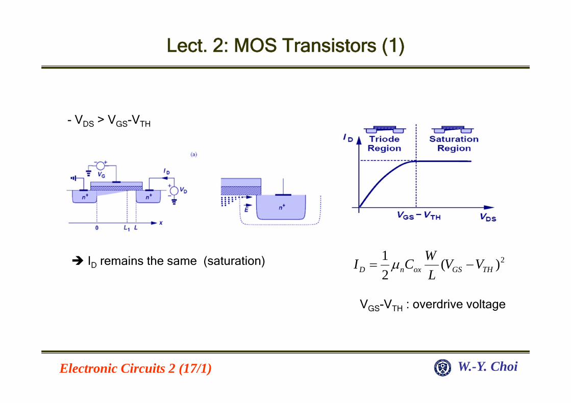
Lect. 2: MOS Transistors (1)
- VDS > VGS-VTH
21 ( )2D n ox GS TH
WI C V VL
ID remains the same (saturation)
VGS-VTH : overdrive voltage

Electronic Circuits 2 (17/1) W.-Y. Choi
Lect. 2: MOS Transistors (1)
- Saturation ( and )GS TH DS GS THV V V V V
- Cut-off ( ), 0GS TH DV V I
-Triode ( and )GS TH DS GS THV V V V V
- NMOS I-V Characteristics
21 2( )2D n ox GS TH DS DS
WI C V V V VL
21 ( )2D n ox GS TH
WI C V VL

Electronic Circuits 2 (17/1) W.-Y. Choi
Lect. 2: MOS Transistors (1)
Triode ( and ) SG TH SD SG THV V V V V
vSD
Saturation ( and )SG TH SD SG THV V V V V
PMOS - VTH < 0
- Holes flow from S to D
- VS > VD
21 2( )2D p ox SG TH SD SD
WI C V V V VL
21 ( )2D p ox SG TH
WI C V VL
- Cut-off ( ), 0SG TH DV V I

Electronic Circuits 2 (17/1) W.-Y. Choi
Lect. 2: MOS Transistors (1)
1) ID really zero in Cut-Off ?
Deviation from the ideal model
Significant problem in modern digital circuits
Leakage between S and D (subthreshold current): More for smaller MOSFET

Electronic Circuits 2 (17/1) W.-Y. Choi
Lect. 2: MOS Transistors (1)
2) In saturation,
VDS increase causes reduction in actual channel length
21 ( ) (1 )2D n ox GS TH DS
WI C VV VL
21 ( )2D n ox GS TH
WI C V VL
But ID increases with VDS even in saturation
Should have no dependence on VDS
Channel length modulation
(Early effect in BJT)

Electronic Circuits 2 (17/1) W.-Y. Choi
Lect. 2: MOS Transistors (1)
3) Body effect
21 ( )2D n ox GS TH
WI C V VL
Voltage applied to B changes threshold voltage
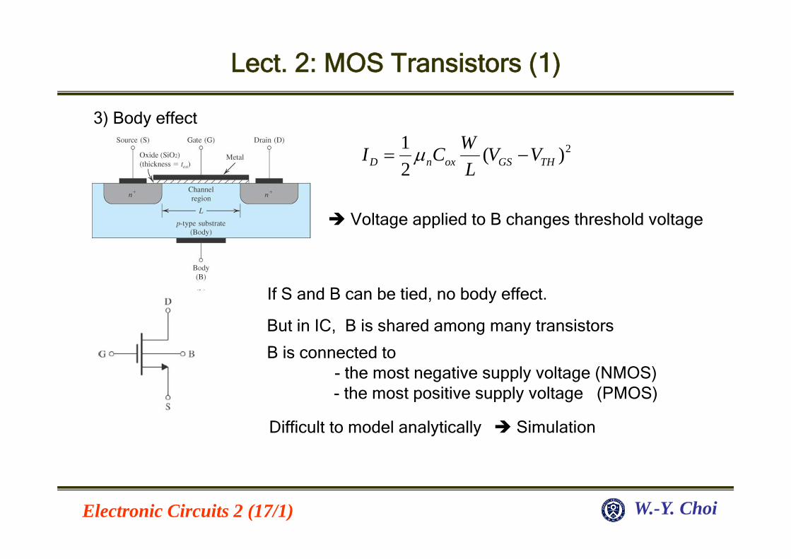
Electronic Circuits 2 (17/1) W.-Y. Choi
Lect. 2: MOS Transistors (1)
3) Body effect
If S and B can be tied, no body effect.
But in IC, B is shared among many transistors
21 ( )2D n ox GS TH
WI C V VL
B is connected to - the most negative supply voltage (NMOS)- the most positive supply voltage (PMOS)
Difficult to model analytically Simulation
Voltage applied to B changes threshold voltage
Electronic Circuits 2 (17/1) W.-Y. Choi
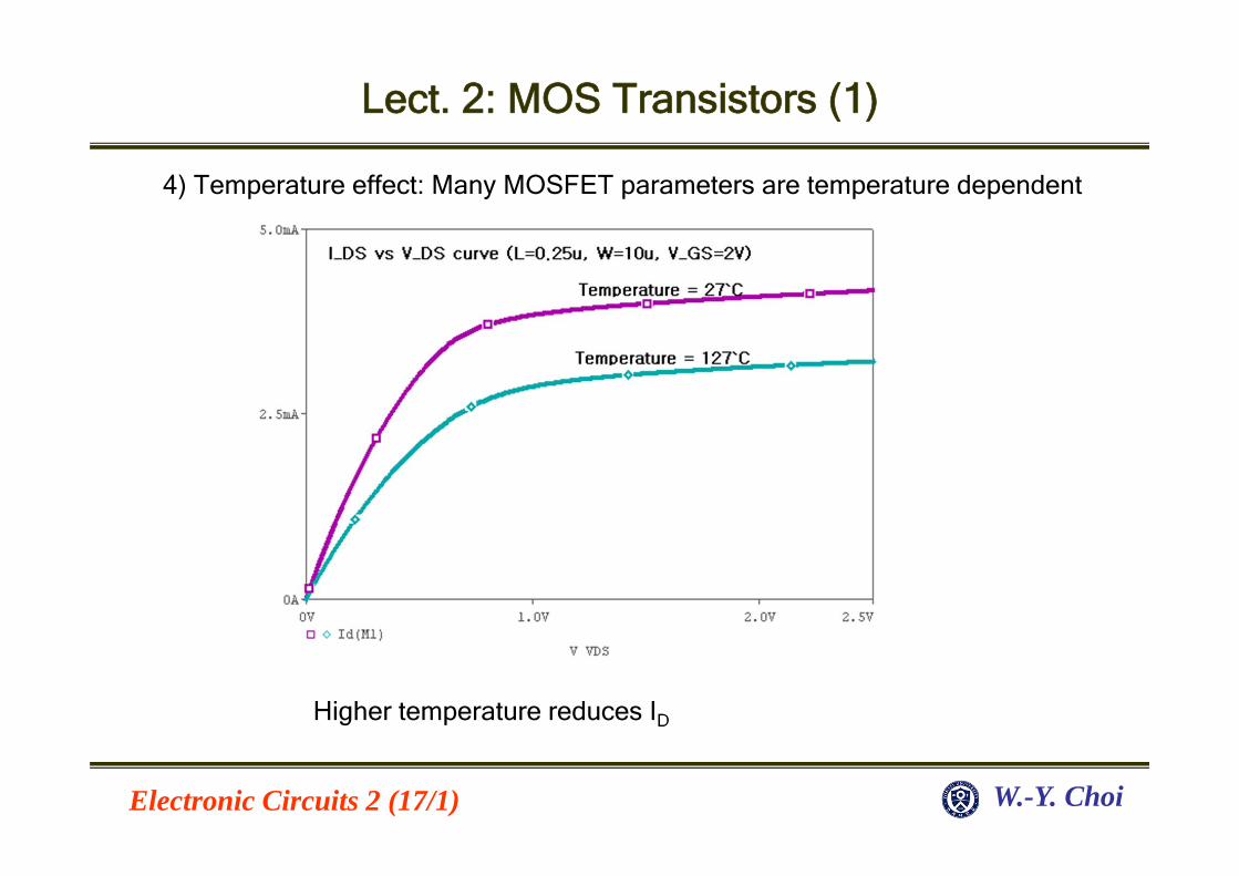
Lect. 2: MOS Transistors (1)
4) Temperature effect: Many MOSFET parameters are temperature dependent
Higher temperature reduces ID

Electronic Circuits 2 (17/1) W.-Y. Choi
Lect. 2: MOS Transistors (1)
- Modern transistors are very complicated in their structure
- Many parameters are needed to model their characteristics accurately in SPICE
- SPICE parameters for 0.25m NMOS are shown on the right
Two-track approach:- Simple, easy-to-use models for analysis- Complicated, accurate models for
simulation
MODEL orbit2L2N NMOS ( LEVEL = 7+TNOM = 27 TOX = 5.6E-9+XJ = 1E-7 NCH = 2.3549E17 VTH0 = 0.3654765+K1 = 0.4732214 K2 = 7.994532E-4 K3 = 1E-3+K3B = 3.0713494 W0 = 1E-7 NLX = 1.617898E-7+DVT0W = 0 DVT1W = 0 DVT2W = 0+DVT0 = 0.455178 DVT1 = 0.6258687 DVT2 = -0.5+U0 = 280.4589023 UA = -1.607126E-9 UB = 2.806549E-18+UC = 3.290051E-11 VSAT = 1.07496E5 A0 = 1.8770435+AGS = 0.3310181 B0 = -3.173524E-8 B1 = -1E-7+KETA = -8.69841E-3 A1 = 8.317145E-5 A2 = 0.6592347+RDSW = 200 PRWG = 0.4477477 PRWB = 0.0208175+WR = 1 WINT = 0 LINT = 1.392558E-10+DWG = -2.28419E-8+DWB = -6.95781E-10 VOFF = -0.0910963 NFACTOR = 1.202941+CIT = 0 CDSC = 2.4E-4 CDSCD = 0+CDSCB = 0 ETA0 = 5.0732E-3 ETAB = 6.262008E-5+DSUB = 0.0310034 PCLM = 1.5101091 PDIBLC1 = 0.897659+PDIBLC2 = 2.924029E-3 PDIBLCB = 0.0651312 DROUT = 1+PSCBE1 = 7.017738E8 PSCBE2 = 2.271109E-4 PVAG = 8.531511E-3+DELTA = 0.01 RSH = 4.6 MOBMOD = 1+PRT = 0 UTE = -1.5 KT1 = -0.11+KT1L = 0 KT2 = 0.022 UA1 = 4.31E-9+UB1 = -7.61E-18 UC1 = -5.6E-11 AT = 3.3E4+WL = 0 WLN = 1 WW = 0+WWN = 1 WWL = 0 LL = 0+LLN = 1 LW = 0 LWN = 1+LWL = 0 CAPMOD = 2 XPART = 0.5+CGDO = 4.59E-10 CGSO = 4.59E-10 CGBO = 5E-10+CJ = 1.78338E-3 PB = 0.99 MJ = 0.4661295+CJSW = 4.154041E-10 PBSW = 0.9563049 MJSW = 0.3162462+CF = 0 PVTH0 = -9.648921E-3 PRDSW = -10+PK2 = 3.534961E-3 WKETA = 0.0120981 LKETA = -3.31688E-3 )