Lech Kupinski Thesis
38
Analysis of the Opto-electronic Properties of Hydrogenated Silicon Carbide using 3D-Ternary diagrams by Lech Kupinski Undergraduate Honours Thesis Faculty of Science (Physics) University of Ontario Institute of Technology Supervisor(s): Dr. Franco Gaspari Copyright c 2014 by Lech Kupinski
-
Upload
lech-kupinski -
Category
Documents
-
view
199 -
download
0
Transcript of Lech Kupinski Thesis
Analysis of the Opto-electronic Properties ofHydrogenated Silicon Carbide using 3D-Ternary diagrams
by
Lech Kupinski
Undergraduate Honours ThesisFaculty of Science (Physics)
University of Ontario Institute of Technology
Supervisor(s): Dr. Franco Gaspari
Copyright c© 2014 by Lech Kupinski
Abstract
Analysis of the Opto-electronic Properties of Hydrogenated Silicon Carbide using
3D-Ternary diagrams
Lech Kupinski
Undergraduate Honours Thesis
Faculty of Science (Physics)
University of Ontario Institute of Technology
2014
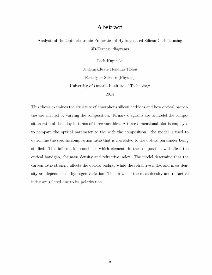
This thesis examines the structure of amorphous silicon carbides and how optical proper-
ties are effected by varying the composition. Ternary diagrams are to model the compo-
sition ratio of the alloy in terms of three variables. A three dimensional plot is employed
to compare the optical parameter to the with the composition. the model is used to
determine the specific composition ratio that is correlated to the optical parameter being
studied. This information concludes which elements in the composition will affect the
optical bandgap, the mass density and refractive index. The model determine that the
carbon ratio strongly affects the optical badgap while the refractive index and mass den-
sity are dependent on hydrogen variation. This in which the mass density and refractive
index are related due to its polarization.
ii

Dedication
I dedicate this to Urszula and Jacek Kupinski
iii
Acknowledgements
who do I want to acknowledge First and foremost I want to thank Dr. Gaspari for all
of his help and guidance in helping me on this thesis. I would also like to thank All of
the UOIT Physics professors for being excellent mentors for young physics majors. The
physics community at this school is small but is full of motivated individials.
I want to knowledge my parents that where always there for me through thick and
thin. The have helped me over than I ever could ask for.
iv
Contents
1 Introduction 1
1.1 Amorphous Silicon . . . . . . . . . . . . . . . . . . . . . . . . . . . . . . . 2
1.1.1 atomic structure . . . . . . . . . . . . . . . . . . . . . . . . . . . . 2
1.1.2 Passivation of a-Si with hydrogen . . . . . . . . . . . . . . . . . . . 3
1.2 Silicon Carbide . . . . . . . . . . . . . . . . . . . . . . . . . . . . . . . . . 3
1.2.1 crystalline silicon carbide . . . . . . . . . . . . . . . . . . . . . . . . 3
1.2.2 amorphous silicon carbide . . . . . . . . . . . . . . . . . . . . . . . 4
1.2.3 Structure of a-SiC:H . . . . . . . . . . . . . . . . . . . . . . . . . . 5
1.3 Effective media approximation . . . . . . . . . . . . . . . . . . . . . . . . . 7
1.4 Mass Density . . . . . . . . . . . . . . . . . . . . . . . . . . . . . . . . . . 7
1.5 Goal . . . . . . . . . . . . . . . . . . . . . . . . . . . . . . . . . . . . . . . 8
2 Optical parametets of Amorphous Silicon Carbides 9
2.1 Optical Bandgap . . . . . . . . . . . . . . . . . . . . . . . . . . . . . . . . 9
2.2 Refractive index . . . . . . . . . . . . . . . . . . . . . . . . . . . . . . . . . 11
3 Analysis with 3 dimensional ternary diagrams 13
3.1 Overview . . . . . . . . . . . . . . . . . . . . . . . . . . . . . . . . . . . . . 13
3.2 Plotting values on Ternary diagrams . . . . . . . . . . . . . . . . . . . . . 14
3.3 3D Ternary Diagrams . . . . . . . . . . . . . . . . . . . . . . . . . . . . . . 14
3.4 Application to aSiC:H . . . . . . . . . . . . . . . . . . . . . . . . . . . . . 16
v
4 results 19
4.1 Experimental Data . . . . . . . . . . . . . . . . . . . . . . . . . . . . . . . 19
4.2 optical bandgap . . . . . . . . . . . . . . . . . . . . . . . . . . . . . . . . . 20
4.3 refractive index . . . . . . . . . . . . . . . . . . . . . . . . . . . . . . . . . 22
4.4 density function . . . . . . . . . . . . . . . . . . . . . . . . . . . . . . . . . 23
5 discussion 25
5.1 optical bandgap . . . . . . . . . . . . . . . . . . . . . . . . . . . . . . . . . 25
5.2 refractive index and mass density function . . . . . . . . . . . . . . . . . . 25
6 conclusion 27
vi
List of Tables
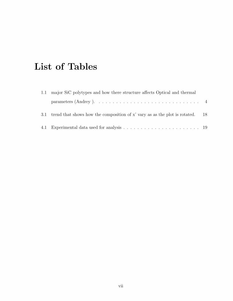
1.1 major SiC polytypes and how there structure affects Optical and thermal
parameters (Andrey ). . . . . . . . . . . . . . . . . . . . . . . . . . . . . . 4
3.1 trend that shows how the composition of x’ vary as as the plot is rotated. 18
4.1 Experimental data used for analysis . . . . . . . . . . . . . . . . . . . . . . 19
vii
List of Figures
1.1 The atomic structure between c-Si and n-Si. Both structures have the same
shortrange order. The lack of long range order in amorphous silcion is a
result of defect states. . . . . . . . . . . . . . . . . . . . . . . . . . . . . . 2
2.1 A comparison of the density of states for n-Si and a-Si:H. n-Si has a distinct
band gap while amorphous silicon does not due to the presence of strained
bonds and dangling bonds. Emobility is determined by the distance between
the localized and and no localized carriers. . . . . . . . . . . . . . . . . . 10
3.1 This example illustrates how to plot data on ternary plots with a given
ratio. . . . . . . . . . . . . . . . . . . . . . . . . . . . . . . . . . . . . . . 14
3.2 These picture show the different the 3D ternary plot at different angles. The
graph on the right displays the relationship between the optical parameter
and the composition . . . . . . . . . . . . . . . . . . . . . . . . . . . . . . 15
3.3 A ternary diagram plotted with the x and y axis . . . . . . . . . . . . . . . 16
3.4 These picture show the different the 3D ternary plot at different angles. The
graph on the right displays the relationship between the optical parameter
and the composition . . . . . . . . . . . . . . . . . . . . . . . . . . . . . . 17
3.5 a) scattered data, no dependence b) linear trend is observed . . . . . . . . 18
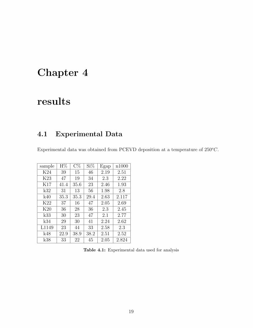
4.1 The data points for the ternary diagram . . . . . . . . . . . . . . . . . . . 20
4.2 This is the linear fit for Eopt at the optimal angle . . . . . . . . . . . . . . 21
viii
4.3 the r value plotted as a function of α for the optical bandgap . . . . . . . . 21
4.4 This is the linear fit for n1000 at the optimal angle . . . . . . . . . . . . . 22
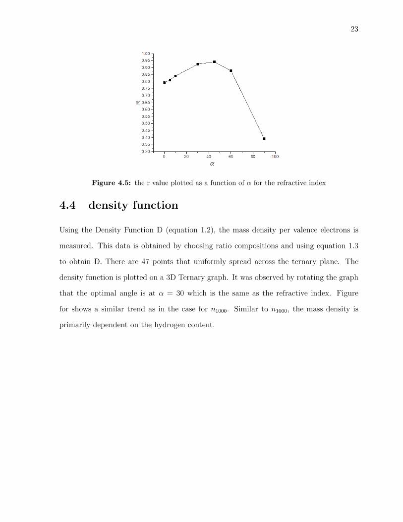
4.5 the r value plotted as a function of α for the refractive index . . . . . . . . 23
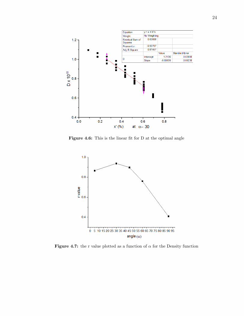
4.6 This is the linear fit for D at the optimal angle . . . . . . . . . . . . . . . 24
4.7 the r value plotted as a function of α for the Density function . . . . . . . 24
ix
Chapter 1
Introduction
Silicon Carbides materials are used as an abrasive and various high temperature, high
temperature applications. More recently the wide band gap and high thermal conductivity
properties make it useful as a semiconductor material for electronic devices designed for
high temperature, high voltage situations. The ability to alter the bandgap in amorphous
silicon carbide by varying it the carbon content in its chemical composition is becoming
an important feature in photovoltaics. Silicon and hydrogen also affect various aspects
of the structure, therefore it is useful to analyse the composition of the entire material
to make accurate predictions of its optical properties. This thesis report contains an
extensive discussion explaining the significance of amorphous silicon and silicon carbides
and the role the structure of the materials has. It is possible to develop a model to study
the effects all three components have on the structure which involves the use of ternary
diagrams. The concept behind ternary diagrams and how they can be used to model
amorphous silicon carbides is explained. Finally, optical parameters are examined with
this method and the contribution of each each elements effects can be made.
1
2
1.1 Amorphous Silicon
1.1.1 atomic structure
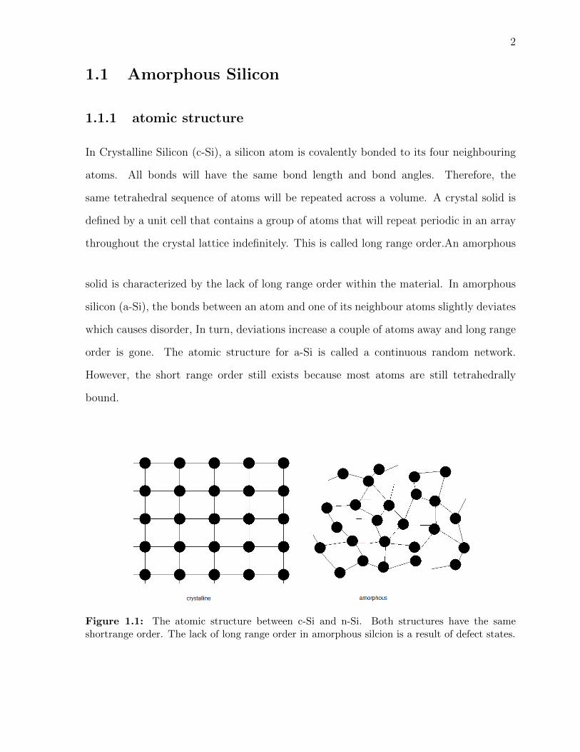
In Crystalline Silicon (c-Si), a silicon atom is covalently bonded to its four neighbouring
atoms. All bonds will have the same bond length and bond angles. Therefore, the
same tetrahedral sequence of atoms will be repeated across a volume. A crystal solid is
defined by a unit cell that contains a group of atoms that will repeat periodic in an array
throughout the crystal lattice indefinitely. This is called long range order.An amorphous
solid is characterized by the lack of long range order within the material. In amorphous
silicon (a-Si), the bonds between an atom and one of its neighbour atoms slightly deviates
which causes disorder, In turn, deviations increase a couple of atoms away and long range
order is gone. The atomic structure for a-Si is called a continuous random network.
However, the short range order still exists because most atoms are still tetrahedrally
bound.
Figure 1.1: The atomic structure between c-Si and n-Si. Both structures have the sameshortrange order. The lack of long range order in amorphous silcion is a result of defect states.
3
1.1.2 Passivation of a-Si with hydrogen
Deviations between silicon atoms can cause the covalent bond to weaken enough for the
bond to break. There are various locations in the material that an Si atom is bonded to
only three neighbours and has an unsatisfied valence, known as a dangling bonds (ch 7) .
the amount of dangling bonds for a-Si is high at 1021cm−3 (Zeman 17). This is not ideal
for photovoltaic applications because when a phonon releases a carrier, there is a greater
change of it being captured by the dangling bond. For this reason, amorphous silicon
is difficult to dope (Zeman 17). (. A-Si is therefore typically passivated with hydrogen,
a process whereby hydrogen atoms are added to the material and bond with unpaired
electrons. The defect density can be lowered to 1015cm−3 when the hydrogen content is
10 % for a-Si:H (Zeman 17)..
1.2 Silicon Carbide
1.2.1 crystalline silicon carbide
Silicon carbide (SiC) is a chemical compound in which carbon and silicon are covalently
bonded. One unique feature of silicon carbides is that they exists in 250 different crys-
talline forms polymorphs (Hornos 8). Since both silicon and carbon are tetrahedral, one
silicon atom is covalently bonded to four carbon, while each carbon atom is again bond
to four different silicon atoms. The structure will be the same in 2 dimensions for all
polymorphs. This is known as a polymorph layer. They can be stacked in multiple ways
which allows for the 250 different polymorphs (Rashed 2). SiC is known as a network
solid because the atoms are held together by a continuous chain of atoms. There are
3 main groups of structures: 3C (α), 4H, (α1)-SiC. 3C (β) follows a stacking order of
ABAB, 4H has an ABCB and (α)-SiC had a sequence ABCACB. The sequence of the
polymorth changes will have a different crystal structure, which determines the band-gap
4
and thermal conductivity (Hornos 8)..
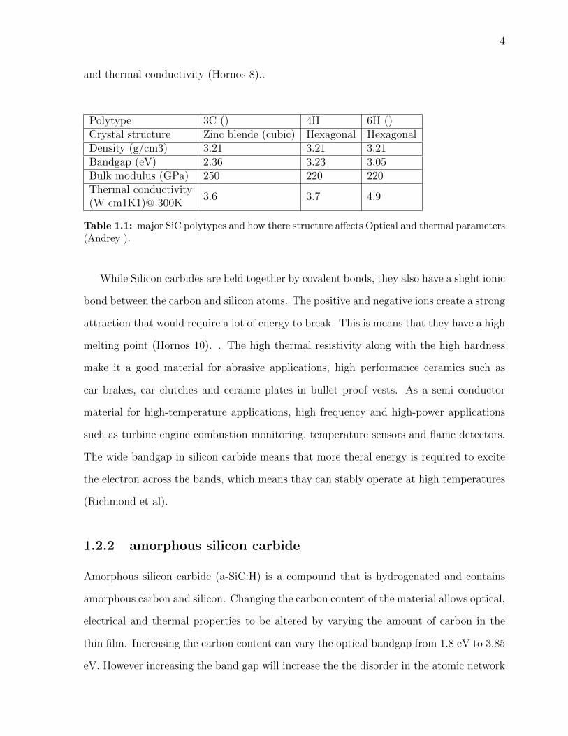
Polytype 3C () 4H 6H ()Crystal structure Zinc blende (cubic) Hexagonal HexagonalDensity (g/cm3) 3.21 3.21 3.21Bandgap (eV) 2.36 3.23 3.05Bulk modulus (GPa) 250 220 220Thermal conductivity(W cm1K1)@ 300K
3.6 3.7 4.9
Table 1.1: major SiC polytypes and how there structure affects Optical and thermal parameters(Andrey ).
While Silicon carbides are held together by covalent bonds, they also have a slight ionic
bond between the carbon and silicon atoms. The positive and negative ions create a strong
attraction that would require a lot of energy to break. This is means that they have a high
melting point (Hornos 10). . The high thermal resistivity along with the high hardness
make it a good material for abrasive applications, high performance ceramics such as
car brakes, car clutches and ceramic plates in bullet proof vests. As a semi conductor
material for high-temperature applications, high frequency and high-power applications
such as turbine engine combustion monitoring, temperature sensors and flame detectors.
The wide bandgap in silicon carbide means that more theral energy is required to excite
the electron across the bands, which means thay can stably operate at high temperatures
(Richmond et al).
1.2.2 amorphous silicon carbide
Amorphous silicon carbide (a-SiC:H) is a compound that is hydrogenated and contains
amorphous carbon and silicon. Changing the carbon content of the material allows optical,
electrical and thermal properties to be altered by varying the amount of carbon in the
thin film. Increasing the carbon content can vary the optical bandgap from 1.8 eV to 3.85
eV. However increasing the band gap will increase the the disorder in the atomic network
5
and lead to degrading electrical properties (Yang 12). Much like the crystalline version,
it is also characterized by high thermal stability and hardness however is can only be
reproduced with small amount of silicon and carbon clusters within the material . Theses
properties make s-SiC:H useful for: anti-reflection coating, surface passivation layer for
crystalline and amorphous silicon solar cells. photo diodes in optical communications and
optical sensors. (Yang 17)
It is typically created by Plasma enhanced vapour deposition using both silane (SiH4)
and methane (CH4) (19). the properties of the material will vary by changing the the
ratio of gases, the pressure and temperature of the subtrate (Joun 19).
1.2.3 Structure of a-SiC:H
The network structure of a-SiC:H is complicated and still not well understood. Since there
are three different elements and both carbon and hydrogen can form tetrahedral bonds,
there are many possible microstructures within the crystal. Ther amount of disorder will
be higher than for a continuous random network in (a-Si:H). This is due to the presenced
of different types of bonds that can exist in the tetrahedral structure of SiC.. The addition
of these type of bonds and bond lengths fromeans that there will be more disorder than
amorphous silicon .(Janz)
Chemical order is defined by the percentage of how much of atom A is bounded to
atom B. For example , 100% order is achieved when all carbon atoms in the thin-film are
only bonded to its neighbouring silicon atoms when the film is described as silicon rich
and likewise for carbon rich. When the film is silicon rich, the Si-C and Si-Si bonds are
randomly distributed. Disorder occurs when the Si and C bond in a randomly throught
the material. There is no definitive order for a-SiC:H due to the variation in the deopsition
process whill affect the chemical structure (Juan 30).
6
Silicon has sp3 hybridization, and has for hybrid bonds with its neighbour atoms. Carbon
can have sp3, sp2, sp1 hybridization, in amorphous carbon ,typically only sp3, sp2 are ob-
served. sp2 hybridization has 3 sp2 orbitals and one un-hybridized orbital. there will be
1 π and 3σ bonds as shown in the figure. Atoms will form a planer structure as opposed
to a tetrahedral structure seen in sp3 hybridization. the addition of π bonds drom carbon
and the various ways ways in which SiC can be arranged will increase the disorder (Wang).
At low carbon concentrations, the carbon atoms do not disturb the tetrahedral struc-
ture of the amorphous silicon network. If the concentrations are equal the most common
bond observed is (Si-C) (Juan). When the carbon content is higher compared to the
silicon content, there is a development of cluster of carbon in the material which contain
C-C bonds. In this case, there are many graphite configurations present.
The Hydrogen content will tend to affect the order of the a-SiC:H. The fact that C-H
bonds are more stable than Si-H bonds will affect the thermal stability of the material.
When a-SiC is hydrogenated more carbond atoms will bond with hydrogen atom than
silicon. Due to the electronegative of silicon and carbon, Si-H bonds will be strengthened
if the silicon atom is bonded to a carbon atom (Juan)
Generally, increasing the amount of hydrogen will saturate the defects and make a
more tetrahedral network. The presences of a certain amount of hydrogen will prevent
the amount of sp2 that occurs if there is also a significant amount of carbon. If the mate-
rial is said to be silicon rich, increasing the amount of hydrogen, the amount Si-Si bonds
will increase as the amount of Si-C will decrease. (Juan)
The different structures that arise at different concentrations will vary the optical and
electrical properties of the structure. This will be discussed in in detail in the next chapter.
7
1.3 Effective media approximation
It is difficult to observe any type of dependence because of the heterogeneous structure
of a-SiC:H. despite having microscopic disorder, a-SiC:H is considered macroscopically
homogeneous. Therefore, the effective media approximation is used to separate the struc-
ture into a large number of uniform regions. Each region has a separate dielectric function
that will combine to form a uniform dielectric function. Also, the sizes of the regions are
small compared to the wavelength of light. (Remes 49)
ε− εhε− Y εh
=∑
fjεj − εhεj − Y εh
(1.1)
Where εj and fj are the dielectric and volume fractions for each section. Y is the host
material is related to the depolarization factor and εh is the effective dielectric constant.
Which approximation model is used the analysis. In this example the Maxwell-Garnett
model or Bruggeman model are used. If the refractive index is known, the absorption co-
efficient can be calculated at one of the volume fractions since all areas are homogeneous.
(Remes 49)
1.4 Mass Density
The mass density is the weight of the film per volume. The atoms in the material can
described as a group of group of uniform point dipoles which can be treated as harmonic
oscillators. The mass density is the thought of as the density of harmonic oscillators. If
the density of oscillators increases, the collective strength of the oscillators will increase
at a particular Eigen frequency (Mergel). In the refractive index section, this is discussed
8
in greater detail.
D =ρ
Nv
=28Si+ 12C +H
Na(4− 3H)(1.2)
The function D is derived in the next chapter and it relates the mass density ρ to
the density of valence electrons. In there research (King) found that mass density was
decreases due to the presence of hydrogen and that the amount of Si-Si and C-C increases
as the mass density decreases.
1.5 Goal
As previously noted, one of the advantages of using silicon carbides is its ability to modify
the contents of the material in order to vary different optical parameters for a specific
device application. The goal of this study is to explore how optical parameters of an
amorphous silicon carbide are affected by the varying the content of Hydrogen, Silicon
and Carbon in a-SiC:H. In many previous research papers the ratio of silicon to carbon
affects different properties of the crystal is studied. The variation of hydrogen and its af-
fects on properties is studied separately. The relationships that develop, such as increased
carbon leading to an increase in the optical gap and the hydrogen content affecting the
refractive index is observed. However, a more complete analysis involves looking at how
properties are affected by varying all three parameters at once. In this paper, a method
involving ternary diagrams is explored. Using experimental data for the strength of a
parameter at a given ratio of hydrogen, silicon and carbon, the ternary method is used
to analyse how the parameter varies at different ratio. This will allow us to observe what
components have the most significant effect on the parameter.
Chapter 2
Optical parametets of Amorphous
Silicon Carbides
In order to tune a-SiC:H material for use for specific devices, it is necessary to look at its
optical behaviour. Optical properties of a-SiC:H are related to the electronic structure
and electronic properties of the material. the optical properties are determined primarily
by studying the absorption coefficient and the band gap. Unlike crystalline semiconduc-
tors, there is no well-defined badgap in amorphous thin films due to the presence of defect
states. However, a bandgap is represented by the energy difference between the two tail
states due to a large reduction in the mobility of carriers. Optical properties are heavily
influenced by the composition of the material. (Zeman 17)
2.1 Optical Bandgap
In crystalline silicon, the band gap is defined between the energy difference between the
valance band and the conduction band where no states are present. as mentioned earlier,
due to the presence of defects in amorphous material, the states between these spread
into the forbbiden gap. The band tail states are a result of strained bonds and the defect
9
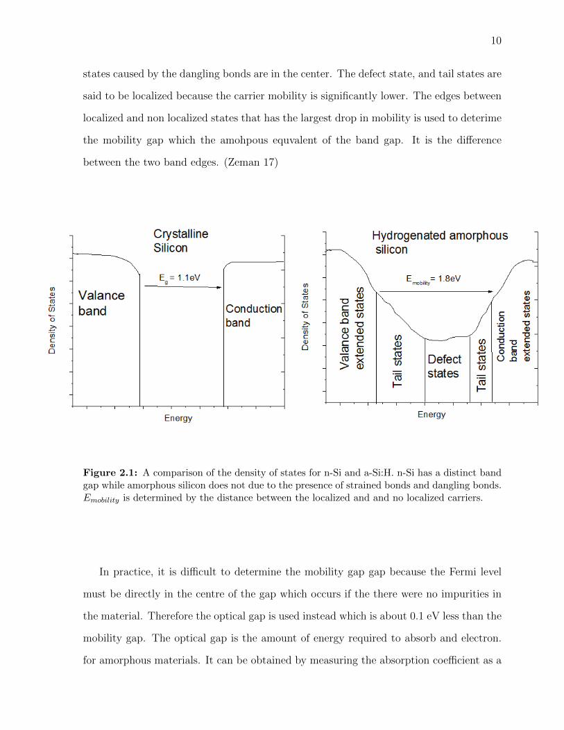
10
states caused by the dangling bonds are in the center. The defect state, and tail states are
said to be localized because the carrier mobility is significantly lower. The edges between
localized and non localized states that has the largest drop in mobility is used to deterime
the mobility gap which the amohpous equvalent of the band gap. It is the difference
between the two band edges. (Zeman 17)
Figure 2.1: A comparison of the density of states for n-Si and a-Si:H. n-Si has a distinct bandgap while amorphous silicon does not due to the presence of strained bonds and dangling bonds.Emobility is determined by the distance between the localized and and no localized carriers.
In practice, it is difficult to determine the mobility gap gap because the Fermi level
must be directly in the centre of the gap which occurs if the there were no impurities in
the material. Therefore the optical gap is used instead which is about 0.1 eV less than the
mobility gap. The optical gap is the amount of energy required to absorb and electron.
for amorphous materials. It can be obtained by measuring the absorption coefficient as a
11
function of photon energy hv. (Zeman 19)
α(hv) = B(hv − Eopt)2 (2.1)
This is called the Tauc optical gap where α(hv) is the abostpion coefficient, Eopt is
the optical gap and B is a constant. The trend is that a material with a higher optical
gap will have a lower absorption coefficient. (Zeman 19)
The optical gap is significantly influenced by the composition of the material of the carbon
content and can vary from 1.8 eV to 3.5 eV. The Optical gap will widen as the carbon
content increases, However, In carbon rich materials, where the carbon to silicon ration
is around 0.65, it is observed that the optical band gap will decrease. This is explained
by the incorporation of graphite like bonds. (Zeman 17)
2.2 Refractive index
The refractive index of a material describes how light is affected by a material and can be
determined by the process of spectroscopic ellipsometry. If the refractive index is known,
the transmission and reflection coefficients can be determined through basic optical calcu-
lations. This will allow us to determine the absorption coefficient and in turn the optical
band gap of the material (Janz).
The refractive index n′ can be written in complex form, n′ = n + ik, where k is the
amount of the electromagnetic wave absorbed, as it passes through a medium. It can be
written in terms of a plane wave travelling in the x direction.(Remes)
E = Eoexp(2πi(ct− ik)
λ) (2.2)
When light travels through a material and it does not have enough energy to excite the
12
electrons to the conduction band the light will be slightly displaced. the reason for this
displacement by bond polarizability ρ(E). The Lorentz-Lorenz equation is able to relate
the refractive index to the polarizability ρ(E) and the density of electrons N . (Remes)
n2 − 1
n2 + 2=
4π
3
∑Niρ(E)i (2.3)
The bounded electrons can be treated as i amount of harmonic oscillators. In terms of a-
SiC:H, all the bonds can be counted as (4Si+4C+H). It is then possible to to relate this
equation to the mass density function.. Substituting the mass density, which is related
to the concentration Ni shows a relationship with the refractive index This is only an
approximation as it assumes a uniform distribution of dipoles. (Remes)
Chapter 3
Analysis with 3 dimensional ternary
diagrams
3.1 Overview
In order to account for the composition of all stoichiometric parameters the idea to use
ternary diagrams was proposed. Ternary diagrams are widely used in fields such as petrol-
ogy, mineralogy and physical chemistry where it is common to study systems with that
are composed of 3 parameters. At ternary diagram is an equilateral triangle with an axis
on each that corresponds to each species. The sum of all the values will sum up to a
constant. The optical parameter that corresponds to the composition is plot along the z
axis.
The 3d graph can be viewed in such a way where the ternary diagram is in the xy
plane with the optical parameter in the z direction. The premises of this method is to loo
analyze the xz plane, where the y axis is the optical data and the x axis is the composition
of material
13
14
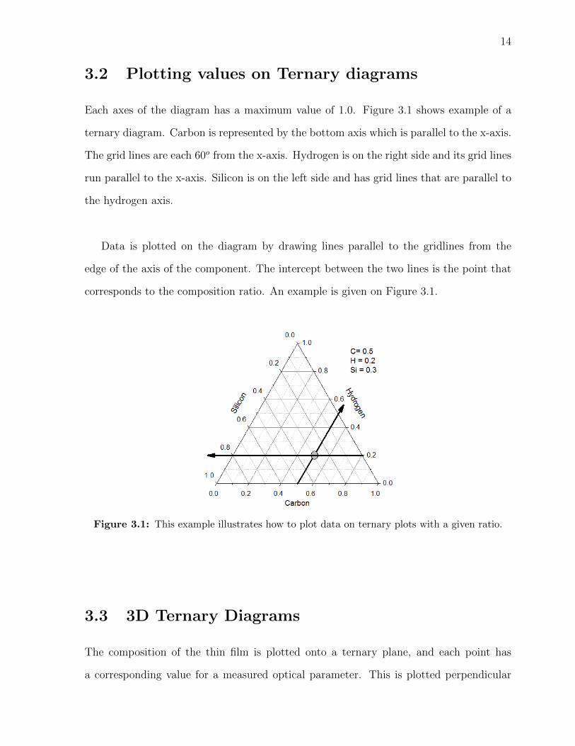
3.2 Plotting values on Ternary diagrams
Each axes of the diagram has a maximum value of 1.0. Figure 3.1 shows example of a
ternary diagram. Carbon is represented by the bottom axis which is parallel to the x-axis.
The grid lines are each 60o from the x-axis. Hydrogen is on the right side and its grid lines
run parallel to the x-axis. Silicon is on the left side and has grid lines that are parallel to
the hydrogen axis.
Data is plotted on the diagram by drawing lines parallel to the gridlines from the
edge of the axis of the component. The intercept between the two lines is the point that
corresponds to the composition ratio. An example is given on Figure 3.1.
Figure 3.1: This example illustrates how to plot data on ternary plots with a given ratio.
3.3 3D Ternary Diagrams
The composition of the thin film is plotted onto a ternary plane, and each point has
a corresponding value for a measured optical parameter. This is plotted perpendicular
15
to the ternary plane in the z direction. To see a trend between the composition and
the optical parameter, the graph is viewed so that the direction of the ternary plane is
perpendicular to the viewing direction. In other words if the ternary diagram is in the
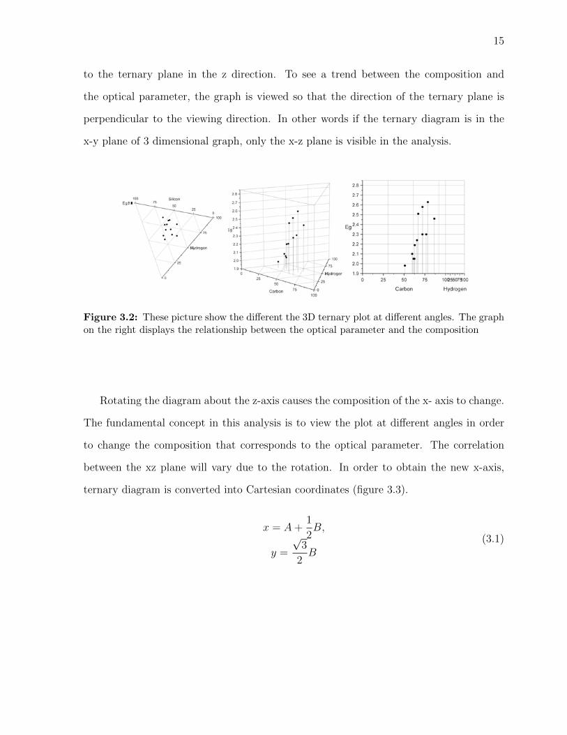
x-y plane of 3 dimensional graph, only the x-z plane is visible in the analysis.
Figure 3.2: These picture show the different the 3D ternary plot at different angles. The graphon the right displays the relationship between the optical parameter and the composition
Rotating the diagram about the z-axis causes the composition of the x- axis to change.
The fundamental concept in this analysis is to view the plot at different angles in order
to change the composition that corresponds to the optical parameter. The correlation
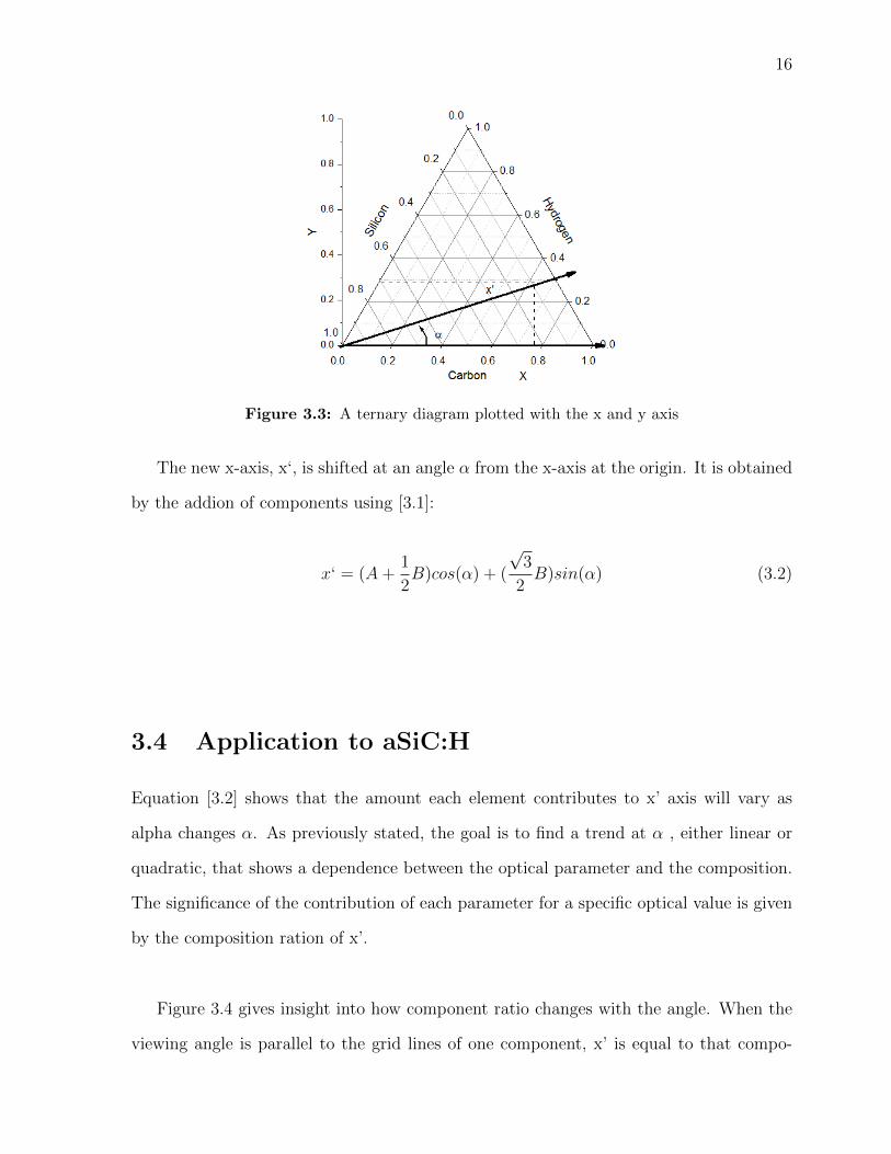
between the xz plane will vary due to the rotation. In order to obtain the new x-axis,
ternary diagram is converted into Cartesian coordinates (figure 3.3).
x = A+1
2B,
y =
√3
2B
(3.1)
16
Figure 3.3: A ternary diagram plotted with the x and y axis
The new x-axis, x‘, is shifted at an angle α from the x-axis at the origin. It is obtained
by the addion of components using [3.1]:
x‘ = (A+1
2B)cos(α) + (
√3
2B)sin(α) (3.2)
3.4 Application to aSiC:H
Equation [3.2] shows that the amount each element contributes to x’ axis will vary as
alpha changes α. As previously stated, the goal is to find a trend at α , either linear or
quadratic, that shows a dependence between the optical parameter and the composition.
The significance of the contribution of each parameter for a specific optical value is given
by the composition ration of x’.
Figure 3.4 gives insight into how component ratio changes with the angle. When the
viewing angle is parallel to the grid lines of one component, x’ is equal to that compo-
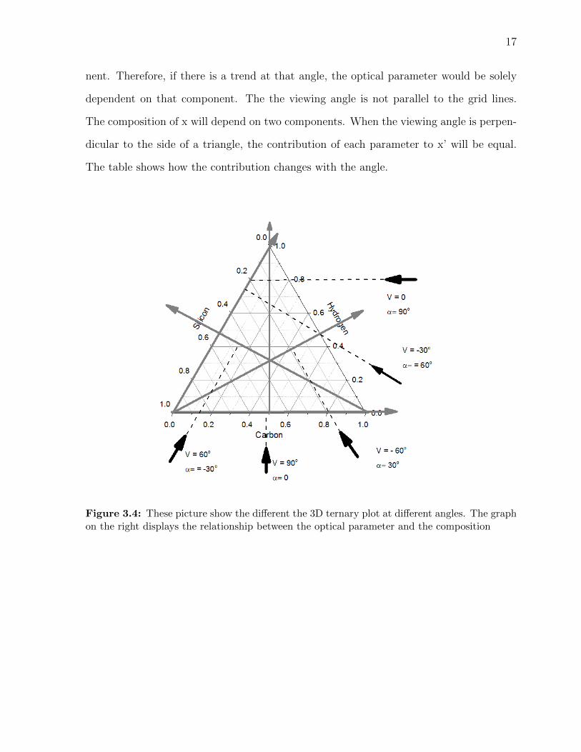
17
nent. Therefore, if there is a trend at that angle, the optical parameter would be solely
dependent on that component. The the viewing angle is not parallel to the grid lines.
The composition of x will depend on two components. When the viewing angle is perpen-
dicular to the side of a triangle, the contribution of each parameter to x’ will be equal.
The table shows how the contribution changes with the angle.
Figure 3.4: These picture show the different the 3D ternary plot at different angles. The graphon the right displays the relationship between the optical parameter and the composition
18
α (degrees) composition of x’(%)
90 H60 Si - H.30 Si0 C- Si
-30 C-60 C-H-90 H
Table 3.1: trend that shows how the composition of x’ vary as as the plot is rotated.
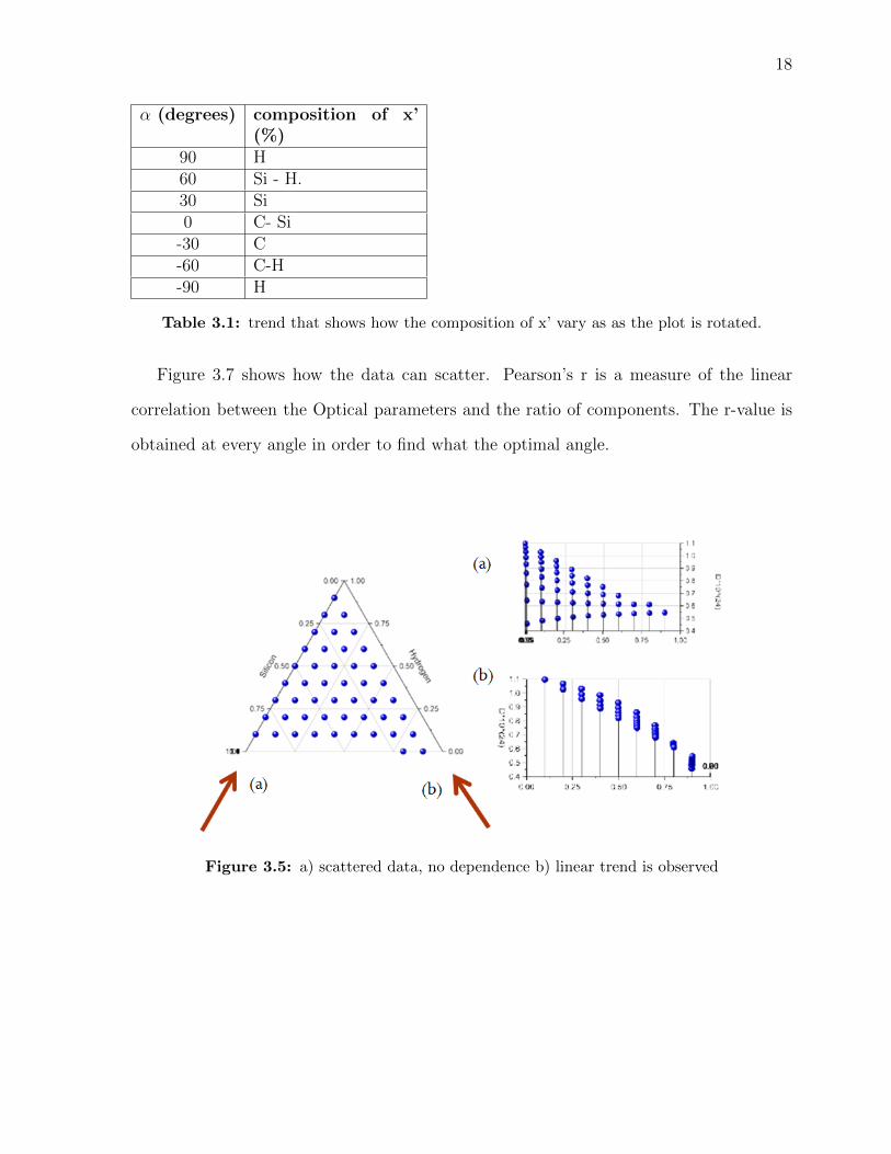
Figure 3.7 shows how the data can scatter. Pearson’s r is a measure of the linear
correlation between the Optical parameters and the ratio of components. The r-value is
obtained at every angle in order to find what the optimal angle.
Figure 3.5: a) scattered data, no dependence b) linear trend is observed
Chapter 4
results
4.1 Experimental Data
Experimental data was obtained from PCEVD deposition at a temperature of 250oC.
sample H% C% Si% Egap n1000K24 39 15 46 2.19 2.51K23 47 19 34 2.3 2.22K17 41.4 35.6 23 2.46 1.93k32 31 13 56 1.98 2.8k40 35.3 35.3 29.4 2.63 2.117K22 37 16 47 2.05 2.69K20 36 28 36 2.3 2.45k33 30 23 47 2.1 2.77k34 29 30 41 2.24 2.62
L1149 23 44 33 2.58 2.3k48 22.9 38.9 38.2 2.51 2.52k38 33 22 45 2.05 2.824
Table 4.1: Experimental data used for analysis
19
20
Figure 4.1: The data points for the ternary diagram
4.2 optical bandgap
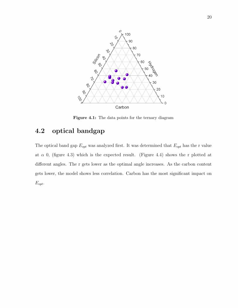
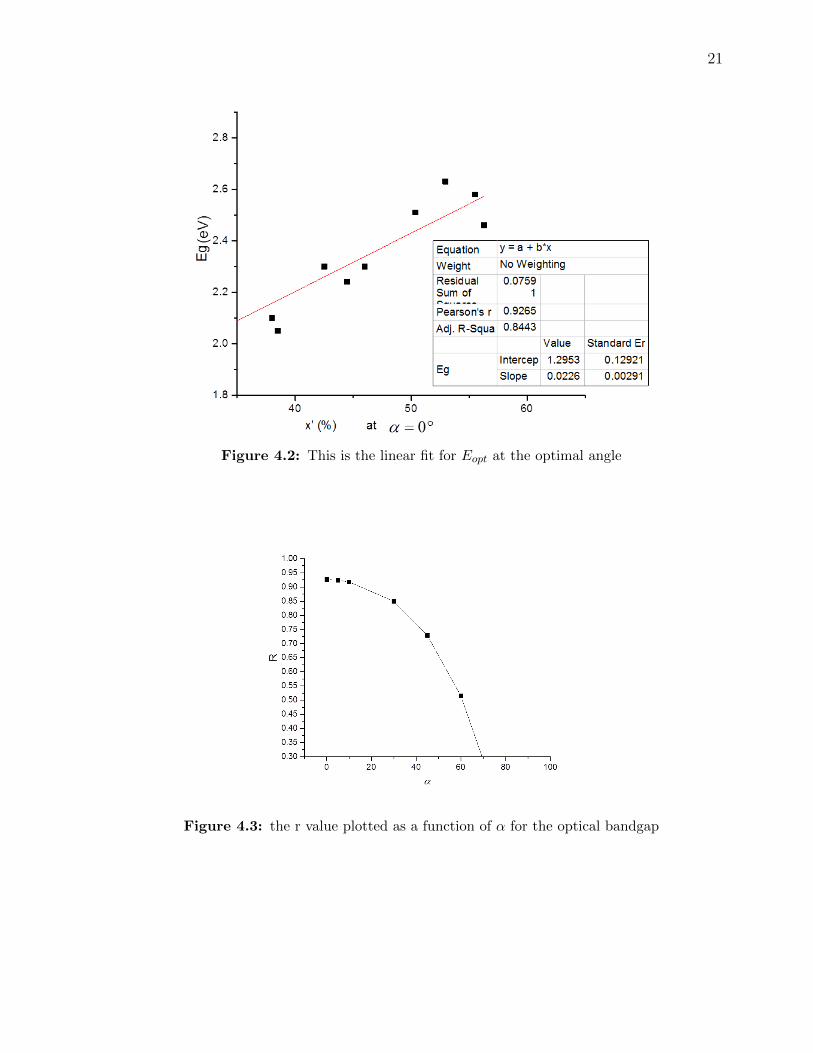
The optical band gap Eopt was analyzed first. It was determined that Eopt has the r value
at α 0, (figure 4.3) which is the expected result. (Figure 4.4) shows the r plotted at
different angles. The r gets lower as the optimal angle increases. As the carbon content
gets lower, the model shows less correlation. Carbon has the most significant impact on
Eopt.
21
Figure 4.2: This is the linear fit for Eopt at the optimal angle
Figure 4.3: the r value plotted as a function of α for the optical bandgap
22
4.3 refractive index
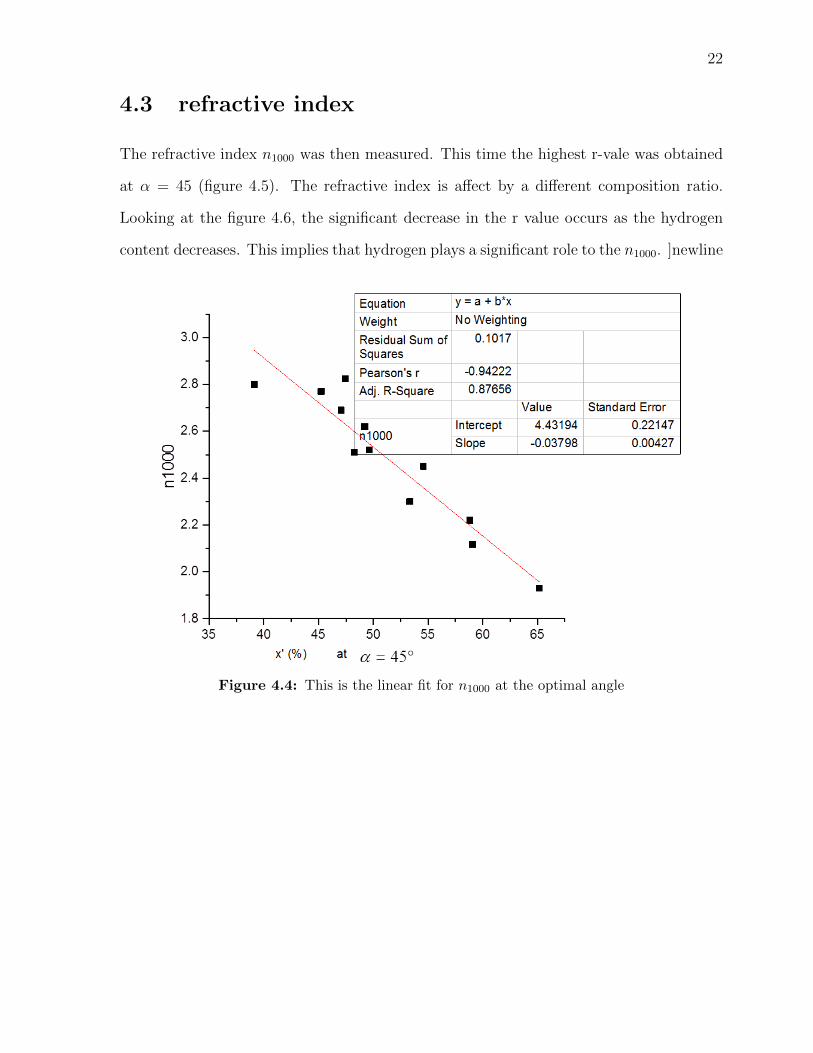
The refractive index n1000 was then measured. This time the highest r-vale was obtained
at α = 45 (figure 4.5). The refractive index is affect by a different composition ratio.
Looking at the figure 4.6, the significant decrease in the r value occurs as the hydrogen
content decreases. This implies that hydrogen plays a significant role to the n1000. ]newline
Figure 4.4: This is the linear fit for n1000 at the optimal angle
23
Figure 4.5: the r value plotted as a function of α for the refractive index
4.4 density function
Using the Density Function D (equation 1.2), the mass density per valence electrons is
measured. This data is obtained by choosing ratio compositions and using equation 1.3
to obtain D. There are 47 points that uniformly spread across the ternary plane. The
density function is plotted on a 3D Ternary graph. It was observed by rotating the graph
that the optimal angle is at α = 30 which is the same as the refractive index. Figure
for shows a similar trend as in the case for n1000. Similar to n1000, the mass density is
primarily dependent on the hydrogen content.
24
Figure 4.6: This is the linear fit for D at the optimal angle
Figure 4.7: the r value plotted as a function of α for the Density function
Chapter 5
discussion
5.1 optical bandgap
The optical band gap was found to have an optimal angle where the most significant
parameter was the C/Si ratio. This corresponds with various experiment results in lit-
erature. Figure 4.5 shows that the r-value decreases as the carbon content decreases.
As carbon content increases the amount of Si-C bonds will increase effectively causing
the optical gap to increase. This is due to the strength of the covalent bond that are
introduced due to the carbon and its tetrahedral bonding. The slope for the linear fit is
positive which implies that the bandgap increase with the carbon content.
5.2 refractive index and mass density function
Unlike Eopt, both the refractive index and the mass density function correlations at higher
α. At this angle, the composition of x’ is only affected by Si and H. This result is signifi-
cant because it shows that n1000 and D are related. This is in line with the theory that is
mentioned in section 2.2. The atoms can be thought of as a group of harmonic oscillators.
The refractive index describes how electromagnetic waves are affected by the frequency
of the atoms. (Choi et al) observed that increasing hydrogen in a-SiC:H will decrease the
25
26
break up the diamond and graphite bonds that leads do a decrease in density. Hydrogen
carbon tends to form tetrahedral bonds while. Boths of these parameters have a negative
slope. This corresponds to literature since an increase in hydrogen decreases the mass
density and intern will decrease the refractive index
This analysis primarily looked at angles between 0 and 90 degrees. However, rotation
between 0 to 90 will show different results. The difference between carbon rich and silicon
rich samples also needs to be addressed. These two different types of samples will have
unique characteristics to them and a result will not repeat similar trends.
Chapter 6
conclusion
Understanding the chemical concentrations of a-SiC:H is crucial in determining the optical
properties. Changing the composition will effect types of bonds present, detects concen-
trations, clustering and bond order. All of these factors will affect the optical parameters.
It has been shown that using 3D ternary diagrams in stoichiometric analysis can success-
fully predict known results about the optical parameters of a-SiC:H. Most analysis of the
a-SiC:H involve looking at the carbon to silicon ratio or the hydrogen concentration. This
analysis is useful for determine the component ratio needed to vary the optical band gap.
Crystalline or amorphous silicon carbide is a material with potential to be useful for a
wide variety of applications due to the hardness of its strong and versatile structure.
27
Bibliography
[Gaspari. 2013] R. Gerhardt*,, Dependence of Optical Parameters on Hydrogenated
Silicon-rich Carbide Alloy Composition: a Ternary-3D Analysis
[Mark. 1987] R. Mark A. Petrich, * Karen K. Gleason, and Jeffrey A. Reimer,, PStructure
and properties of amorphous hydrogenated silicon carbide PHYSICAL REVIEW B.
VOLUME 36, NUMBER 18 15 DECEMBER 1987-II
[Gerhardt. 2011] R. Gerhardt*,, Properties and Applications of Silicon Carbide Copyright
2011 InTech ,Janeza Trdine 9, 51000 Rijeka, Croatia).
[King. 2011] R. S.W. King a,, J. Bielefeld a, M. French a, W.A. Lanford,, Mass and bond
density measurements for PECVD a-SiCx:H thin films using Fourier transform-infrared
spectroscopy Journal of Non-Crystalline Solids 357 (2011) 36023615.
[Janz. 2006] Stefan Janz, Amorphous Silicon Carbide for Photovoltaic Applications
(Fraunhofer Institut fr Solare Energiesysteme, Freiburg, 2006).
[Juan.(2000)] Juan H, “STRUCTURAL AND ELECTRICAL CHARACTERISATIONS
OF AMORPHOUS SILICON CARBIDE FILMS,” NATIONAL UNIVERSITY OF
SINGAPORE, 2000.
[Gulses(2004)] A GLuses.(2004). ”ELLIPSOMETRIC AND UV-VIS TRANSMIT-
TANCE ANALYSIS OF AMORPHOUS SILICON CARBIDE THIN FILMS”. Physical
Review
28
29
[Wang.(2009)] L. Wang, P.R China. *, ”Depostion and Characterisation of Amorphous
and Nanocrystalline SiC”, September 2009
[Rene.(1999)] Z Rene,. Study of defects and microstructure of amorphous and microcrys-
talline silicon thin films and polycrystalline diamond using optical methods. Faculty of
Mathematics and Physics of the Charles University. 1999
[Ca.(2011)] Figure taken from Elliptic Composability
[Ambrosone G. 2011] G. Ambrosone*,1,2, D.K. Basa3, U. Coscia2,4, A. Le Donne5, and
S. Binetti5, Role of carbon content in tuning the physical quantities of a-Si1-xCx:H
alloys deposited by PECVD Phys. Status Solidi C, 2011).
[Mergel(2009)] Dieter Mergel1 and Martin Jerman (2009). ”Density and refractive index
of thin evaporated films”. CHINESE OPTICS LETTERS
[Yang. 2011] G. Ambrosone*,1,2, D.K. Basa3, U. Coscia2,4, A. Le Donne5, and S. Cheng-
Chieh Yang, Hydrogenated Amorphous Silicon Carbide Prepared using DC Saddle Field
PECVD for Photovoltaic Applications Graduate Department of Electrical and Com-
puter Engineering University of Toronto).
[Thevaril . 2011] J. Thevaril,, The Optical Response of Hydrogenated Amorphous Silicon
University of Windsor,, 2011).
[Jazizadeh. 2013] B. Jazizadeh*,, Stoichiometric Hydrogenated Amorphous Silicon Car-
bide Thin Film Synthesis Using DC-Saddle Plasma Enhanced Chemical Vapour Depo-
sition University of Toronto , 2013).
[Zemen. 2010] Zemen,, Chapter 7. Thin-Film Silicon Solar Cells Delft University of Tech-
nology , 2010).