lec3 single stage - Laboratoire d'informatique de Paris 6hassan/lec3_single_stage.pdf · • B....
24
1 Single Stage Amplifiers •Basic Concepts •Common Source Stage •Source Follower •Common Gate Stage •Cascode Stage Hassan Aboushady University of Paris VI • B. Razavi, “Design of Analog CMOS Integrated Circuits”, McGraw-Hill, 2001. References H. Aboushady University of Paris VI
Transcript of lec3 single stage - Laboratoire d'informatique de Paris 6hassan/lec3_single_stage.pdf · • B....

1
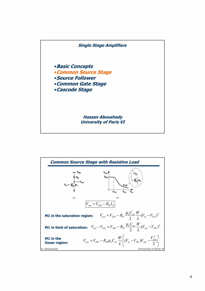
Single Stage Amplifiers
•Basic Concepts•Common Source Stage•Source Follower•Common Gate Stage•Cascode Stage
Hassan AboushadyUniversity of Paris VI
• B. Razavi, “Design of Analog CMOS Integrated Circuits”,McGraw-Hill, 2001.
References
H. Aboushady University of Paris VI

2
Single Stage Amplifiers
•Basic Concepts•Common Source Stage•Source Follower•Common Gate Stage•Cascode Stage
Hassan AboushadyUniversity of Paris VI
Basic Concepts I
H. Aboushady University of Paris VI
• Amplification is an essential function in most analog circuits !
• Why do we amplify a signal ?
• The signal is too small to drive a load• To overcome the noise of a subsequent stage• Amplification plays a critical role in feedback systems
In this lecture:• Low frequency behavior of single stage CMOS amplifiers:• Common Source, Common Gate, Source Follower, ...
• Large and small signal analysis.• We begin with a simple model and gradually add 2nd order effects
• Understand basic building blocks for more complex systems.

3
Approximation of a nonlinear system
H. Aboushady University of Paris VI
212
210 )(...)()()( xxxtxtxtxty nn ≤≤++++≈ αααα
)()( 10 txty αα +≈
Input-Output Characteristic of a nonlinear system
In a sufficiently narrow range:
where α0 can be consideredthe operating (bias) point andα1 the small signal gain
Analog Design Octagon
H. Aboushady University of Paris VI
4
Single Stage Amplifiers
•Basic Concepts•Common Source Stage•Source Follower•Common Gate Stage•Cascode Stage
Hassan AboushadyUniversity of Paris VI
Common Source Stage with Resistive Load
H. Aboushady University of Paris VI
2)(2 THinoxn
DDDout VVLWCRVV −−= µ
211 )(
2 THinoxn
DDDTHin VVLWCRVVV −−=− µ
⎥⎦
⎤⎢⎣
⎡−−−=
2)(
2out
outTHinoxnDDDoutVVVV
LWCRVV µ
DDDDout IRVV −=
M1 in the saturation region:
M1 in limit of saturation:
M1 in thelinear region:

5
Common Source Stage with Resistive Load
H. Aboushady University of Paris VI
)(1 THinDoxn
DD
Don
onDDout
VVRLWC
VRR
RVV−+
=+
=µ
M1 in deeplinear region:
Common Source Stage with Resistive Load
H. Aboushady University of Paris VI
Dm
THinoxnDin
outv
Rg
VVLWCR
VVA
−=
−−=∂∂= )(µ
2)(2 THinoxn
DDDout VVLWCRVV −−= µ
M1 in the saturation region:
Small signal gain:
Same relation can be derivedfrom the small signal equivalentcircuit
Small signal model forthe saturation region
To minimize nonlinearity, the gain equation must be a weakfunction of signal dependent parameters such as gm !

6
Example 1
H. Aboushady University of Paris VI
Sketch ID and gm of M1 as a function of the Vin:
• M1 in the saturation region:
2)(2 THinoxn
D VVLWCI −= µ
)( THinoxnGS
Dm VV
LWC
VIg −=
∂∂= µ
• M1 in the linear region:
⎥⎦
⎤⎢⎣
⎡−−=
2)(
2
1out
outTHinoxnDVVVV
LWCI µ
outoxnGS
Dm V
LWC
VIg µ=
∂∂=
)(1 THinDoxn
DDout
VVRLWC
VV−+
=µ
Voltage Gain of a Common Source Stage
H. Aboushady University of Paris VI
D
RDDoxnv IVI
LWCA µ2−=
Dmv RgA −=
How to increase Av ?
Trade-offs:
• Increase W/L Greater device capacitances.
• Increase VRD Limits Vout swing.
• Reduce ID Greater Time Constant.
D
RDoxnv I
VLWCA µ2−=
7
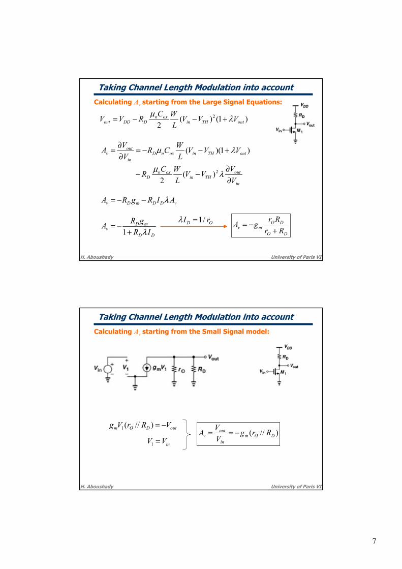
Taking Channel Length Modulation into account
H. Aboushady University of Paris VI
)1()(2
2outTHin
oxnDDDout VVV
LWCRVV λµ +−−=
in
outTHin
oxnD
outTHinoxnDin
outv
VVVV
LWCR
VVVLWCR
VVA
∂∂−−
+−−=∂∂=
λµ
λµ
2)(2
)1)((
DO
DOmv Rr
RrgA+
−=OD rI /1=λ
vDDmDv AIRgRA λ−−=
DD
mDv IR
gRAλ+
−=1
Calculating Av starting from the Large Signal Equations:
Taking Channel Length Modulation into account
H. Aboushady University of Paris VI
outDOm VRrVg −=)//(1
inVV =1
)//( DOmin
outv RrgVVA −==
Calculating Av starting from the Small Signal model:

8
Example 2
H. Aboushady University of Paris VI
Assuming M1 biased in saturation,calculate the small signal voltage gain :
• I1 : Ideal current source Infinite Impedance
Omv rgA −=
• Intrinsic gain of a transistor:This quantity represents the maximum voltagegain that can be achieved using a single device.
12
1 )1()(2
IVVVLWCI outTHin
oxnD =+−= λµ
• Constant Current:As Vin increases, Vout must decrease such that theproduct remains constant
CS Stage with Current-Source Load
H. Aboushady University of Paris VI
)//( 21 OOmv rrgA −=• Both transistors operate in the saturation region:
• The output impedance and the minimumrequired VDS of M2 are less strongly coupled thanthe value and voltage drop of a resistor.
22min,2 THGSDS VVV −=
• This value can be reduced to a few hundred millivolts bysimply increasing the width of M2.•If rO2 is not sufficiently high, the length and width of M2 can beincreased to achieve a smaller λ while maintaining the sameoverdrive voltage.•The penalty is the large capacitance introduced by M2 at theoutput node.•Increasing L2 while keeping W2 constant increases rO2 andhence the voltage gain, but at the cost of higher |VDS2|required to maintain M2 in saturation

9
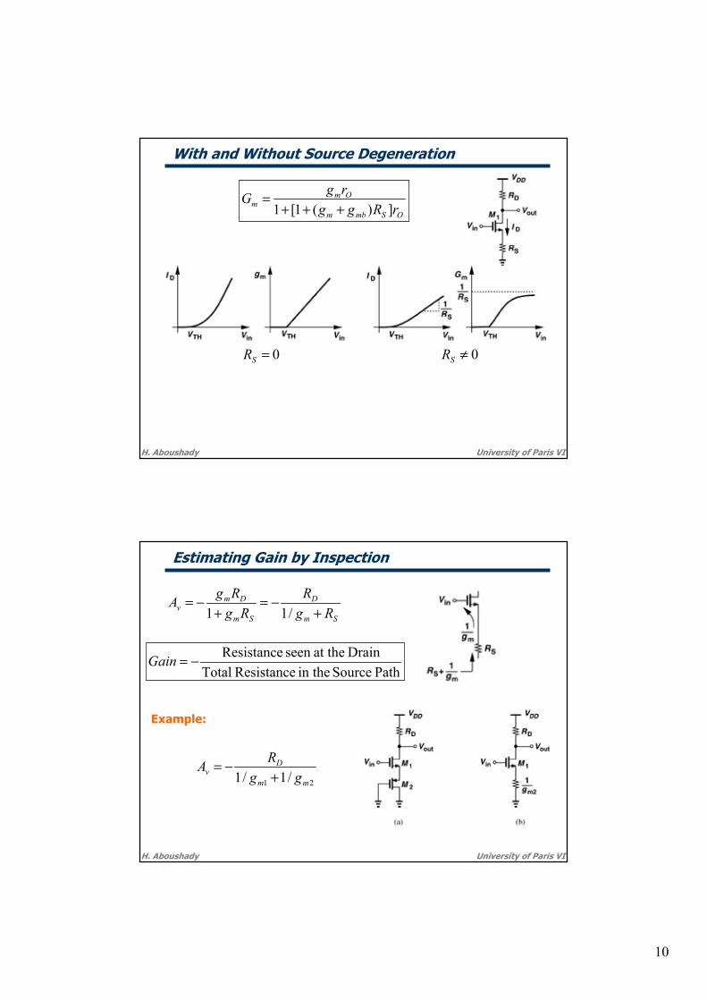
CS with Source Degeneration
H. Aboushady University of Paris VI
in
GS
GS
D
in
Dm V
VVI
VIG
∂∂
∂∂=
∂∂=
SDinGS RIVV −=
Sin
D
in
GS RVI
VV
∂∂−=
∂∂ 1
( )mSmm
in
DS
GS
Dm
GRgGVIR
VIG
−=
⎟⎟⎠
⎞⎜⎜⎝
⎛∂∂−
∂∂=
1
1
GS
Dm V
Ig∂∂=
Sm
mm Rg
gG+
=1 Dmv RGA −=
Sm
Dmv Rg
RgA+
−=1
Large Signal model: Small Signal model:
Sm
m
in
Dm RVgV
VgVIG
11
1
+==
Sm
mm Rg
gG+
=1
CS with Source Degeneration
H. Aboushady University of Paris VI
SmSm
mm RgRg
gG+
=+
=/1
11 mS gRfor /1>> Sm RG /1≈
ID is linearized at the cost of lower gain.
Small Signal model including body effectand channel length modulation:
O
SoutSoutmbSoutinm
O
XXmbmout
rRIRIgRIVg
rVVgVgI
−−+−=
−−=
)()(
1
OSmbmS
Om
in
outm rRggR
rgVIG
])(1[ +++==
10
With and Without Source Degeneration
H. Aboushady University of Paris VI
OSmbm
Omm rRgg
rgG])(1[1 +++
=
0=SR 0≠SR
Estimating Gain by Inspection
H. Aboushady University of Paris VI
Sm
D
Sm
Dmv Rg
RRgRgA
+−=
+−=
/11
Example:
PathSourcein the ResistanceTotalDrain at theseen Resistance−=Gain
21 /1/1 mm
Dv gg
RA+
−=
11
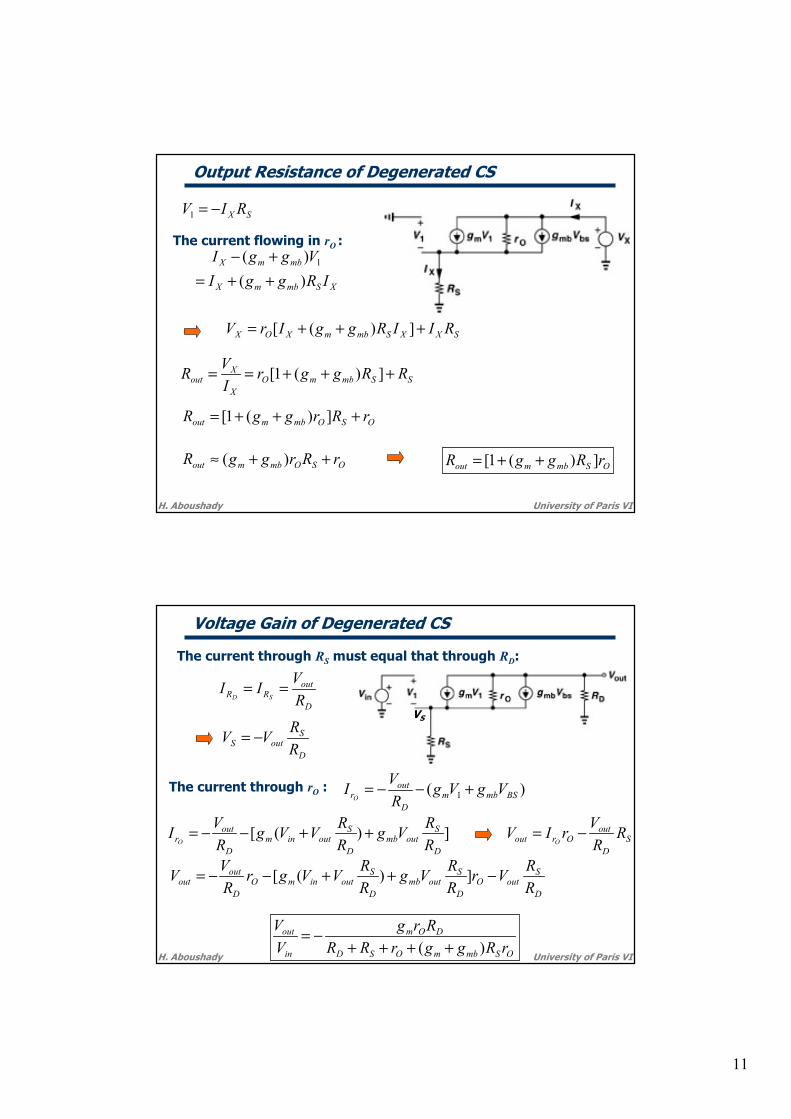
Output Resistance of Degenerated CS
H. Aboushady University of Paris VI
SX RIV −=1
XSmbmX
mbmX
IRggIVggI
)()( 1
++=+−
The current flowing in rO :
SXXSmbmXOX RIIRggIrV +++= ])([
SSmbmOX
Xout RRggr
IVR +++== ])(1[
OSOmbmout rRrggR +++= ])(1[
OSOmbmout rRrggR ++≈ )( OSmbmout rRggR ])(1[ ++=
Voltage Gain of Degenerated CS
H. Aboushady University of Paris VI
)( 1 BSmbmD
outr VgVg
RVI
O+−−=
])([D
Soutmb
D
Soutinm
D
outr R
RVgRRVVg
RVI
O++−−=
The current through RS must equal that through RD:
D
outRR R
VIISD
==VS
D
SoutS RRVV −=
The current through rO :
SD
outOrout R
RVrIV
O−=
D
SoutO
D
Soutmb
D
SoutinmO
D
outout R
RVrRRVg
RRVVgr
RVV −++−−= ])([
OSmbmOSD
DOm
in
out
rRggrRRRrg
VV
)( ++++−=

12
Voltage Gain of Degenerated CS
H. Aboushady University of Paris VI
OSmbmOSD
DOm
in
out
rRggrRRRrg
VV
)( ++++−=
OSmbmOSD
OSmbmOSD
OSmbmS
Om
in
out
rRggrRRrRggrRR
rRggRrg
VV
)(])([
])(1[ +++++++
+++−=
The output resistanceof a degenerated CS stage:
OSmbmout rRggR ])(1[ ++=
The Transconductanceof a degenerated CS stage:
( )Doutmin
out RRGVV //=
OSmbmS
Om
in
outm rRggR
rgVIG
])(1[ +++==
General expression to calculate Av by inspection
H. Aboushady University of Paris VI
Gm : the transconductance ofthe circuit when the output isshorted to grounded.
outmRGAv −=
Lemma:
Rout : the output resistanceof the circuit when the inputvoltage is set to zero.
• For high voltage gain the output resistance must be high!A “buffer” is needed to drive a low-impedance load.The source follower can operate as a voltage buffer.
13
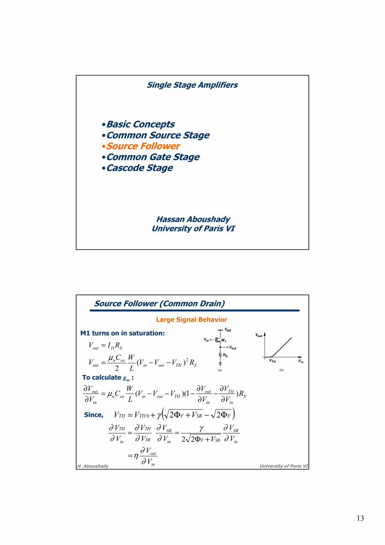
Single Stage Amplifiers
•Basic Concepts•Common Source Stage•Source Follower•Common Gate Stage•Cascode Stage
Hassan AboushadyUniversity of Paris VI
Source Follower (Common Drain)
H. Aboushady University of Paris VI
STHoutinoxn
out RVVVLWCV 2)(
2−−= µ
Sin
TH
in
outTHoutinoxn
in
out RVV
VVVVV
LWC
VV )1)((
∂∂−
∂∂−−−=
∂∂ µ
M1 turns on in saturation:
SDout RIV =
To calculate gm :
in
out
in
SB
SBFin
SB
SB
TH
in
TH
VV
VV
VVV
VV
VV
∂∂η
∂∂γ
∂∂
∂∂
∂∂
=
+Φ==
22
( ) 220 FSBFTHTH VVV Φ−+Φ+= γSince,
Large Signal Behavior

14
Source Follower Voltage Gain
H. Aboushady University of Paris VI
)1()(1
)(
ηµ
µ
+−−+
−−=
∂∂
STHoutinoxn
STHoutinoxn
in
out
RVVVLWC
RVVVLWC
VV
)( THoutinoxnm VVVLWCg −−= µ
Smbm
Sm
RggRgAv
)(1 ++=
Sin
TH
in
outTHoutinoxn
in
out RVV
VVVVV
LWC
VV )1)((
∂∂−
∂∂−−−=
∂∂ µ
Sin
out
in
outTHoutinoxn
in
out RVV
VVVVV
LWC
VV )1)((
∂∂−
∂∂−−−=
∂∂ ηµ
We also have,
Source Follower Voltage Gain
H. Aboushady University of Paris VI
Smbm
Sm
in
out
RggRg
VVAv
)(1 ++==
Small Signal Equivalent Circuit
[ ][ ] Soutmboutinm
SBSmbmout
RVgVVgRVgVgV
−−=+=
)(1
mmb gg η=Since:
)1(1η+
≈Av
And for : 1>>SmRg

15
Source Follower Output Resistance
University of Paris VI
0=−− XmbXmX VgVgImbmX
Xout ggI
VR+
== 1
Rout : the output resistance when the input voltage is set to zero.
Body Effect decreases the output resistance of source followers.
H. Aboushady
↑⇒
↓↑⇒↓
D
THGSX
IVandVV
XBS VVV −==1
Source Follower body effect
H. Aboushady University of Paris VI
mbmmbmout ggggR
+== 11//1
Small Signal Model Simplification
Note that the value of the current source gmbVbs is linearlyproportional to the voltage across it.
Rout : the output resistance when the input voltage is set to zero.

16
Source Follower Thévenin Equivalent
H. Aboushady University of Paris VI
mbm
m
mbm
mbv gg
g
gg
gA+
=+
= 11
1
H. Aboushady University of Paris VI
Channel Length Modulation in M1 and M2
mLOO
mb
LOOmb
gRrr
g
RrrgAv 1//////1
//////1
21
21
+=

17
Source Follower Characteristics
University of Paris VI
PMOS source follower with VSB=0
- Nonlinearity
SBTH VV α
outnoutp
mnmpnp
RRgg
>⇒
<⇒< µµ
H. Aboushady
- Limited voltage swing
+ High input impedance and Moderate output impedance
Example:
11 THGSX VVV −>Without the source follower stage:
With the source follower stage:)( 332 THGSGSX VVVV −+>
Low Load Impedance: CS vs SF
H. Aboushady University of Paris VI
mL
LvSF gR
RA/1+
≈ LmvCS RgA −≈
2/1≈vSFA 1−≈vCSA
Source Followers are not necessarily efficient drivers.
Source Follower Amplifier Common Source Amplifier
Assuming RL=1/gm

18
Single Stage Amplifiers
•Basic Concepts•Common Source Stage•Source Follower•Common Gate Stage•Cascode Stage
Hassan AboushadyUniversity of Paris VI
Common Gate Stage
H. Aboushady University of Paris VI
DTHinboxn
DDout RVVVLWCVV 2)(
2−−−= µ
Din
THTHinboxn
in
out RVVVVV
LWC
VV
⎟⎟⎠
⎞⎜⎜⎝
⎛∂∂−−−−−=
∂∂ 1)(µ
( ) DTHinboxnin
out RVVVLWC
VV ηµ +−−=
∂∂ 1)(
Large Signal Behavior
Assuming M1 in saturation:
DDDDout RIVV −=
Dmv RgA )1( η+=

19
Common Gate Stage Input Resistance
H. Aboushady University of Paris VI
Body Effect:• increases Av• decreases Rin
Same as Output Resistance of Source Follower:
mbmin ggR
+= 1
Common Gate Gain
H. Aboushady University of Paris VI
01 =+− inSD
out VRRVV
outinSD
outmbm
D
outO VVR
RVVgVg
RVr =+−⎟⎟
⎠
⎞⎜⎜⎝
⎛−−−
11
Small Signal Signal Equivalent Circuit
The current through RS is equal to -Vout / RD :
The current through rO is equal to -Vout / RD - gmV1 - gmbV1 :
outinSD
outin
D
Soutmbm
D
outO VVR
RVV
RRVgg
RVr =+−⎥
⎦
⎤⎢⎣
⎡⎟⎟⎠
⎞⎜⎜⎝
⎛−+−− )(

20
Common Gate Gain
H. Aboushady University of Paris VI
DSOmbmOSD
OmbmvCG R
RrggrRRrggA
)(1)(
++++++=
DSOmbmOSD
OmvCS R
RrggrRRrgA
)( ++++−=
Common Gate Amplifier:
Degenerated Common Source Amplifier:
Common Gate Stage Input Resistance
H. Aboushady University of Paris VI
Since V1 = -VX :
[ ]XmbmXOXDX VggIrIRV )( +−+=
)(1
)(
)(1
mbmOmbm
Din
Ombm
OD
X
X
ggrggRR
rggrR
IV
++
+≈
+++=
• Assume RD = 0 :
)(/11
mbmOin ggrR
++=
• Replace RD by ideal current source:
∞=inR
Rin of a common gate stage is low only if RD is small.

21
Common Gate Stage Output Impedance
H. Aboushady University of Paris VI
( ) DOSOmbmout RrRrggR //])(1[ +++=
Similar to Output Impedance of aDegenerated Common Source Stage
Single Stage Amplifiers
•Basic Concepts•Common Source Stage•Source Follower•Common Gate Stage•Cascode Stage
Hassan AboushadyUniversity of Paris VI

22
Biasing of a Cascode Stage
H. Aboushady University of Paris VI
The cascade of CS stage and a CG stage is called “cascode”.
M1 : the input deviceM2 : the cascode device
Biasing conditions:• M1 in saturation:
2GSbX VVV −=
12 THinGSb VVVV −≥−
2THXbXout VVVVV −−≥−
12 THGSinb VVVV −+≥
221 THGSTHinout VVVVV −+−≥
• M2 in saturation:
Cascode Stage Characteristics
H. Aboushady University of Paris VI
Large signal behavior:As Vin goes from zero to VDDFor Vin < VTH M1 and M2 are OFF
Vout =VDD
21222 ])(1[ OOOmbmout rrrggR +++=
Output Resistance:• Same common source stage witha degeneration resistor equal to rO1
1222 )( OOmbmout rrggR +≈
• M2 boosts the output impedance of M1by a factor of gmr02
• Triple cascode difficult biasing at low supply voltage.
↑↑outR

23
Cascode Stage Voltage Gain
H. Aboushady University of Paris VI
outmRGAv −=
1mm gG ≈
1222 )( OOmbmout rrggR +≈
11222 )( OmOmbmv rgrggA +≈
Ideal Current Source:
Cascode Current Source:
433122 // OOmOOmout rrgrrgR ≈
( )4331221 // OOmOOmmv rrgrrggA ≈
Shielding Property
H. Aboushady University of Paris VI
Assume VX is higher than VY by ∆V.Calculate the resulting difference between ID1 and ID2 (with λ ≠ 0 ).
)()(2 21
221 DSDSTHb
oxnDD VVVV
LWCII λλµ −−=−
)()(2
221 DSTHb
oxnDD VVV
LWCII ∆−=− λµ
33331333
1
)(])(1[ OmbmOOOmbm
OPQ rgg
Vrrrgg
rVV+∆≈
+++∆=∆
333
221 )(
)(2 Ombm
THboxn
DD rggVVV
LWCII
+∆−=− λµ

24
Folded Cascode
H. Aboushady University of Paris VI
Simple Folded Cascode
Folded Cascodewith biasing
Folded Cascodewith NMOS input
Large Signal Characteristics:
Output Resistance of Folded Cascode
H. Aboushady University of Paris VI
231222 )//]()(1[ OOOOmbmout rrrrggR +++=
1111 ])(1[ OSOmbmout rRrggR +++=
Degenerated Common Source Stage:
Folded Cascode Stage:
M1 M2
RS rO1 // rO3