Learn More Email / defensesales@curtisswright · Sensors for monitoring board power consumption ......
13
Learn More Web / cwcdefense.com/sales Email / [email protected] cwcdefense.com Data Sheet Onboard PCIe Gen3 switch - One 8-lane secondary expansion plane (P5) fabric ports to the backplane - One 4-lane connection to each FPGA - One 4-lane connection to the processor Onboard SRIO Gen2 switch - Four 4-lane fabric ports to the backplane - 4-lane ports to each FPGA - 4-lane port to ARM Processor via an SRIO-PCIe bridge Xilinx ZYNQ FPGA with Dual ARM Cortex A9 processor - 1 GB DDR3L SDRAM - 256 MB application flash - 32 MB boot flash with 32 MB Alt boot flash - 128KB NvRAM - One Gigabit Base-T Ethernet links to the backplane P4 connector or Front Panel - One Gigabit Base-X Ethernet links to the backplane P4 connector - One RS-232 links to the backplane or Front Panel - One x4 Gen2 PCIe connection from the processor to the Gen3 PCIe switch - 8 SE and 4 differential DIO to backplane - Option for Trusted Platform Module (TPM) Thermal sensors for monitoring board temperatures Sensors for monitoring board power consumption Support for ChipScope ™ Pro and JTAG processor debug interfaces CHAMP-FX4 (VPX6-473) Xilinx ® Tri-Virtex ® -7 6U OpenVPX ™ Module Features OpenVPX ™ (VITA 65) profile MOD6-PAY- 4F1Q2U2T-12.2.1-11, VPX REDI (VITA 48 option) Three user-programmable Xilinx Virtex-7 FPGAs (585T or X690T), each with: - 4 GB DDR3L SDRAM in two 64-bit banks - 36 MB QDRII+ SRAM in two 36-bit banks - Path to 72 MB /per FPGA - Three 10.3 GHz 4-lane serial links to the backplane from each IO FPGA or one of the x4 links can be optionally connected to the FMC site - Four 10.3 GHz 4-lane serial links to the Expansion plane from the Aggregator FPGA - Six 10.3 GHz serial links between the three FPGAs - One 4-lane SRIO Gen2 link to the onboard switch fabric - One 4-lane Gen3 PCIe target host link from onboard PCIe switch - 8 LVDS pairs to the backplane from each I/O FPGA - 20 LVDS pairs to the backplane from the Aggregator FPGA - 10/20 differential pairs between each FPGA - FMC connection with 80 differential pairs or 4/8 serial links to each site to support JESD204B or serial FMCs - Each FPGA can be configured via Local attached flash, via SelectMap from processor, or via PCIe - 32 MB attached configuration flash Two FMC interfaces with 80 differential signal pairs - Each site supports 4/8 high speed serial links for JESD204B or Serial FMCs
Transcript of Learn More Email / defensesales@curtisswright · Sensors for monitoring board power consumption ......

Learn MoreWeb / cwcdefense.com/sales Email / [email protected]
cwcdefense.com
Dat
a Sh
eet
�� Onboard PCIe Gen3 switch�- One 8-lane secondary expansion plane (P5) fabric
ports to the backplane�- One 4-lane connection to each FPGA�- One 4-lane connection to the processor
�� Onboard SRIO Gen2 switch
�- Four 4-lane fabric ports to the backplane
�- 4-lane ports to each FPGA �- 4-lane port to ARM Processor via an SRIO-PCIe
bridge
�� Xilinx ZYNQ FPGA with Dual ARM Cortex A9 processor�- 1 GB DDR3L SDRAM�- 256 MB application flash�- 32 MB boot flash with 32 MB Alt boot flash�- 128KB NvRAM
�- One Gigabit Base-T Ethernet links to the backplane P4 connector or Front Panel
�- One Gigabit Base-X Ethernet links to the backplane P4 connector
�- One RS-232 links to the backplane or Front Panel�- One x4 Gen2 PCIe connection from the processor to
the Gen3 PCIe switch
�- 8 SE and 4 differential DIO to backplane
�- Option for Trusted Platform Module (TPM)
�� Thermal sensors for monitoring board temperatures
�� Sensors for monitoring board power consumption
�� Support for ChipScope™ Pro and JTAG processor debug interfaces
CHAMP-FX4 (VPX6-473)
Xi l inx® Tr i -Vir tex®-7
6U OpenVPX™ Module
Features
�� OpenVPX™ (VITA 65) profile MOD6-PAY- 4F1Q2U2T-12.2.1-11, VPX REDI (VITA 48 option)
�� Three user-programmable Xilinx Virtex-7 FPGAs (585T or X690T), each with:
�- 4 GB DDR3L SDRAM in two 64-bit banks�- 36 MB QDRII+ SRAM in two 36-bit banks�- Path to 72 MB /per FPGA
�- Three 10.3 GHz 4-lane serial links to the backplane from each IO FPGA or one of the x4 links can be optionally connected to the FMC site
�- Four 10.3 GHz 4-lane serial links to the Expansion plane from the Aggregator FPGA
�- Six 10.3 GHz serial links between the three FPGAs�- One 4-lane SRIO Gen2 link to the onboard switch
fabric�- One 4-lane Gen3 PCIe target host link from onboard
PCIe switch�- 8 LVDS pairs to the backplane from each I/O FPGA�- 20 LVDS pairs to the backplane from the Aggregator
FPGA�- 10/20 differential pairs between each FPGA�- FMC connection with 80 differential pairs or 4/8
serial links to each site to support JESD204B or serial FMCs
�- Each FPGA can be configured via Local attached flash, via SelectMap from processor, or via PCIe
�- 32 MB attached configuration flash
�� Two FMC interfaces with 80 differential signal pairs
�- Each site supports 4/8 high speed serial links for JESD204B or Serial FMCs
Curtiss-Wright Controls Defense Solutions / cwcdefense.com
Overview
The CHAMP-FX4 is the flagship 6U product in Curtiss-Wright Controls Defense Solutions’ family of user-programmable Virtex®-7 FPGA-based computing products, designed to meet the needs of challenging embedded high-performance digital signal and image processing applications. Curtiss-Wright's 4th generation 6U FPGA card, the CHAMP-FX4 combines the dense processing resources of three large Xilinx® Virtex®-7 FPGAs with over 12 GB of memory resources, all on a rugged 6U OpenVPX™ (VITA 65) form factor module. The CHAMP-FX4 complements this processing capability with vast amounts of backplane I/O bandwidth, exceeding 100 GB/s, directly connected to the FPGAs. Gen2 Serial RapidIO® (SRIO) provides standards-based connectivity to general-purpose processing boards such as the VPX6-1957 and CHAMP-AV8. In addition, 36 pairs of LVDS links to the backplane can be used to support Camera Link or other high-speed parallel interfaces. There are also two FMC sites that have been enhanced to support the next generation of serial or JESD204B FMC cards, providing a configuration option to support up to 8 lanes of SERDES connectivity to each site. A Xilinx ZYNQ FPGA with embedded dual Arm Cortex A9 processors provides powerful command and control
2
�� Common Backplane clock/sync paths to all FPGAs
�� Multi-board synchronous clock
�� FXTools BSP and FPGA design kit with highly-optimized IP Blocks, development environment, reference designs, scriptable simulation test benches and software libraries VxWorks® and Linux® variants available
�� Continuum IPC – inter-processor communications middleware available
�� Backplane I2C/IPMI control for power on/off card and sensor information
�� VITA 48 1” pitch format
�� Ruggedization levels
�- Level 0 (Commercial)�- Air-cooled level 100 �- Conduction-cooled level 200
capability in a compact footprint. Using the CHAMP-FX4 with Curtiss-Wright’s Signal Acquisition FMC cards such as the FMC-516/FMC-518 provides a complete Digital Receiver solution. With no onboard FPGA, FMCs are a low power mezzanine option and can better handle extreme rugged conditions. Furthermore, with the flexibility of the FMC interface, alternate front ends can be accommodated by using different FMC modules. (*See note)
This combination of enormous processing density and I/O flexibility makes the CHAMP-FX4 an ideal choice for many commercial or rugged embedded applications, including radar and signal intelligence, image or network processing, and for intelligence, surveillance and reconnaissance (ISR) platforms, providing more than twice the performance of the previous generations of FPGA products.
Xilinx Virtex-7 FPGAs
FPGAs provide parallel processing capabilities, reducing processor count and system size. Operations such as FFTs, FIR filters and other fixed-point and/or repetitive processing tasks are highly suited for placement inside FPGAs.
At the heart of the CHAMP-FX4 are three Xilinx Virtex-7 FPGAs in the FFG1761 package, one of the larger FPGAs in the Virtex-7 family. This package is 42.5 mm x 42.5 mm and supports 850 SelectIO pins and 36 Highspeed SERDES pairs. The -2 speed grade is used to provide the maximum performance over the full industrial temperature range. The two FPGA die supported are the X690T and the 585T. The X690T is a DSP focused FPGA with large amounts of DSP blocks and Block Ram. The 585T is a pin compatible part with a smaller die and primarily optimized with general purpose logic.
Two of the Virtex-7 FPGAs are called “I/O” FPGAs as they are connected to FMC mezzanine sites as well as backplane SERDES. The third Virtex-7 FPGA is connected to the Backplane Expansion Plane and is called the “Aggregator” FPGA. A simplified block diagram is shown in Figure 1.
*See the FMC section of this data sheet for specific information regarding compatible FMCs for the CHAMP-FX4.
Curtiss-Wright Controls Defense Solutions / cwcdefense.com
BlockRam has been increased to approximately 53 Mb in the X690T device which is about 40% more than what was available in the SX475T Virtex-6 device. The BlockRam architecture maintains the same dual 18Kb or single 36Kb block structure. They can be configured as single or dual port memories and contain built-in FIFO logic and 64-bit ECC. One new feature is the ability to disable power to unused memories.
FPGA Resource Summary
Table 1 below summarizes the amount of different FPGA resources with the different FPGA options available for the CHAMP-FX4. This information is directly from Xilinx datasheets.
FPGA Architecture
The CHAMP-FX4 has been architected to maximize FPGA processing capability, I/O and memory bandwidth to support applications which require large amounts of front-end parallel sensor processing. I/O can be passed to the card via the dual FMC sites or via the multiple back plane serial links. Support for Gen2 SRIO, Gen3 PCIe, and OpenVPX, as well as Aurora links up to 10.3 Gbps, provide multiple options for transferring data between similar FPGA cards or to other general purpose processing cards or GPGPU cards.
The CHAMP-FX4 has three Virtex-7 FPGA devices.
Memory
Each Virtex-7 on the CHAMP-FX4 has two wide 64-bit memory interfaces which use fast DDR3L memory. Each bank is 2 GB with a possible future upgrade path to 4 GB. Running at a minimum of 600 MHz DDR (1.2 Gbps), the two memory banks provide at least 9.6 GB/s of peak
Figure 1: High Level Block Diagram
CHAMP-FX4
x16 SRDSx20 LVDS
x12 SRDSx8 LVDS
x16
FMC FMC
x12 SRDSx8 LVDS
Gen3PCIeSwitch
Gen2SRIOSwitch
P2SBridge
I/OFPGA
I/OFPGA
UserPlane
DataPlane
ExpansionPlane
CtlPlane
UserPlane
ZYNQSubsystem
AggrFPGA
The X690T and 585T devices offer 690K and 582K logic cells respectively, providing significantly more capacity than the largest DSP Virtex-6 device. The V7 slice is the same 4-LUT, 8-FF architecture as was used on the Virtex-6. The only significant change is that the POR (Power-on-Reset) and PROG (Program) signal now clears both LUT RAMs and SRLs. Optimizations have been made to the routing interconnect logic and with the routing tools. This results in a more compacted design within an area of the FPGA allowing much better utilization of the FPGA logic resources.
DSP slices have been increased to 3600 in the X690T device, almost double the number of DSP slices available in the largest DSP Virtex-6 device. The DSP slice is the exact same architecture as on the Virtex-6, so any Virtex-6 designs utilizing the DSP blocks can be ported directly.
3
Table 1: CHAMP-FX4 FPGA ResourceLogic Resources Memory Resources Clock Resources Embedded Hard IP Resources & Speed Grades
Slices Logic Cells
CLB Flip-Flops
Max. Dist. RAM (kbits)
Block RAM/FIFO w/ ECC (36 kbits each)
Total Block RAM (kbits)
Mixed Mode Clock Manager
(MMCM)
DSP48E Slices
PCIe Endpoint Blocks
Speed Grade
RocketIO GTH (run at 10.3
GHz or lower)
585T 91,050 582,720 728,400 6,938 795 28,620 18 1,260 3 -2C, -2I 36
X690T 108,300 693,120 866,400 10,888 1,470 52,920 20 3,600 3 -2C, -2I 36
Notes* Two of the 585T banks are HR banks instead of HP banks. These two banks are connected to the FMC site and limit FMC usage. X690T variant is recommended when using FMCs. Contact factory for details.** Also contact factory if a two FPGA option is desired.

Curtiss-Wright Controls Defense Solutions / cwcdefense.com
memory bandwidth per bank. Full thermal characterization will determine the final supported speed which may be as high as 800 MHz or 12.8 GB/s of potential peak memory bandwidth per bank. Note that due to SDRAM latency, actual throughput is very dependent on data block transfer size. The larger the data blocks, the closer to the theoretical maximum throughput can be achieved as inter-block gaps are minimized.
Each Virtex-7 on the CHAMP-FX4 also has two 36-bit QDRII+ dual port memory banks (36b read and 36b write). Each bank is 18 MB and runs at 500 MHz DDR (1.0 Gbps). A future growth path to 36 MB is supported. The devices used in the standard configuration support a burst size of 4 words, and a read latency of 2.5 cycles to maximize memory bandwidth.
See Figures 2 and 3 for detailed views of the I/O FPGAs and the Aggregator FPGA
FPGA Backplane and Inter-FPGA I/O
The FPGA nodes on the CHAMP-FX4 have 36 SERDES that are used for different functions.
One of the x4 GTH SERDES links is dedicated to a Gen3 x4 PCIe link which is connected to a Gen3 PCIe switch.
This path is generally used as the host interface into the FPGA from the local ZYNQ FPGA which contains the embedded dual ARM processors. It is also interconnected to an x8 PCIe interface on the backplane P5 connector and can be controlled by any processor board that has a PCIe link to the secondary expansion plane (P5) such as the VPX6-1957 or CHAMP-AV8. Note that a physical path from the processor to the P5 is required to support this host path.
This path could also be used for the FPGA to transmit data. Contact factory for PCIe DMA capability on this interface.
One of the x4 GTH SERDES links is dedicated to a Gen2 x4 SRIO link which is connected to a Gen2 SRIO switch. This path is generally used as a data path to pass data to a general purpose processor such as the VPX6-1957 or CHAMP-AV8 via the SRIO switch which is connected to the data plane on the back plane. This interface supports 5 Gbps maximum data rate. DMA capability is provided inside the FPGA to either stream data out from memory or from an internal data pipeline. The DMA capability also includes inline doorbell generation capability to provide seamless far-end notification of data transmission.
12 (IO FPGA) or 16 (Aggregator FPGA) other GTH SERDES links are connected directly to the back plane. Because these signals are directly connected to the FPGA they can
4
Figure 2: FPGA Memory & I/O (I/O FPGA)
DDR3LSDRAM
X64(2GB/ea)
Virtex-7XC7VX690T or
XC7V585T(1761 pin pkg)
FMCSite x4 PCIe Gen3
Host Interface
x6 SERDES(to other I/O FPGA)
x20 LVDS prs(to Aggregator FPGA)
x8 LVDSBackplane
QSPIFlash256Mb
x80LVDS(prs)
x4/x8SERDES
(2)
QDRII+SRAMX36
(32MB/ea)
(2) x6 SERDES(to Aggregator FPGA)
x10 LVDS prs(to other I/O FPGA)
x12 SERDESBackplane
x4 Gen2SRIO Switch
SelectMap
ZYNQ DIO (4)
Figure 3: FPGA Memory & I/O (Aggregator FPGA)
DDR3LSDRAM
X64(2GB/ea)
Virtex-7XC7VX690T or
XC7V585T(1761 pin pkg)
x4 PCIe Gen3Host Interface
x6 SERDES(to I/O FPGA 1)
x20 LVDS prs(to IO FPGA 2)
x20 LVDSBackplane
(2)
QDRII+SRAMX36
(32MB/ea)
(2) x6 SERDES(to I/O FPGA 2)
x20 LVDS prs(to I/O FPGA 1)
x16 SERDESBackplane
x4 Gen2SRIO Switch
SelectMap
ZYNQ DIO (4)
QSPIFlash256Mb
*The CHAMP-FX4 card is being fully qualified over the full rugged temperature range. These interfaces are being characterized to determine their maximum reliable operating frequencies over that temperature range. The included numbers are the target values, but could change based on actual results. For SerDes interfaces, the maximum speeds are only supported on card or thru a properly designed backplane and are not guaranteed thru an RTM (rear transition module). Contact factory for more information.

Curtiss-Wright Controls Defense Solutions / cwcdefense.com
support any protocol, depending on what FPGA IP core is utilized inside the FPGA. The default configuration is to support Aurora, but other options such as PCIe, SRIO, 10/40 GbE are also possible. These SERDES can run up to 10.3 Gbps. Note that while PCIe can be supported with a PCIe core inside the FPGA, it requires a build variant as the line termination is different than the other protocols. Please contact factory if that option is desired.
These SERDES on the Aggregator FPGA are directly connected to the Expansion Plane (P2) connector. On an OpenVPX backplane that implements the daisy-chained expansion plane, these signals can be used to pass data between adjacent slots hosting other FX4 cards. If a backplane is being used that does not rout the Expansion Plane, these SERDES can be accessed via the CHAMP-FX4 Rear Transition Module (RTM).
These SERDES on the I/O FPGA are split between the P4, P5 and P6 connectors which are part of the User Plane. While these signals are not generally routed on a standard backplane, they can either be accessed using the CHAMP-FX4 RTM or with a custom backplane.
The remaining x12 GTH SERDES links are split into two groups of 6 and connect each of the FPGAs together. These links can also run up to 10.3 Gbps. Note that if additional inter-FPGA SERDES links are required, some of the backplane links can be used to pass data between the FPGAs. This can be done via the CHAMP-FX4 RTM or via a custom backplane.
The backplane SERDES all have access to a fixed 312.5 MHz oscillator and a SiLabs SI570 Programmable clock. Combining these different potential reference clocks with the configurable multiply/divide settings for each quad-SERDES provides maximum flexibility for potential line rates. Configuration of the programmable clock can be done through the V7 FPGA via an I2C interface.
The Virtex-7 has Xilinx’x latest generation 2D eye scan capability that enables visibility right at the SERDES receiver. The observation point is also after equalization so that the effects of equalization can also be seen. Xilinx now has an RX Margin Analysis tool which can characterize the receive channel. Control for the SERDES are also accessible in the reference design for customer tuning as needed. This extra controllability and visibility is essential when bringing up multi-gigabit signals on the backplane.
In addition to the SERDES links there are LVDS pairs that go to the backplane. The Aggregator FPGA has 20 LVDS pairs that go to the P3 connector, 3 of which are clock capable. Each of the I/O FPGAs has 8 LVDS pairs that go the P6 connector, 2 of which are clock capable. Between the two I/O FPGAs there are 10 differential pairs and between each of the I/O FPGAs and the Aggregator there are 20 differential pairs. These signals are user configurable for any low latency data that need to be passed between the FPGAs.
OpenVPX also defines a common 25 MHz reference clock, a 1 PPS clock, and a RES_BUS_SE signal that can be used as a sync signal. These 3 signals are all connected to the ZYNQ FPGA and are routed to the 3 Virtex-7 FPGAs.
There is also a common LVDS backplane clock pair which is routed through a low skew buffer to all 3 FPGAs.
FPGA Configuration
Each Virtex-7 has a 256 Mb QSPI Flash device connected to it for initial configuration. The FPGA and Flash can also be programmed directly with JTAG. The ZYNQ FPGA has two 128 MB banks of QSPI Flash for non-volatile storage of application code or bit file images. There is also 1 GB of DDR3 SDRAM for volatile storage. Images stored in Flash or SDRAM can be loaded into the Virtex-7 FPGAs using SelectMap programming. Using Tandem configuration it is also possible to program the FPGA directly via the PCIe bus from the host processor. Lastly the QSPI Flash can be programmed via software using a QSPI core inside the FPGA.
Configuration time will be dependent on FPGA option, whether or not compression is used and whether or not the image is encrypted. The worst case is the X690T FPGA with no compression and encryption which can take about 1 second assuming a 100 MHz configuration clock. Without encryption, but no compression, configuration time will be about 600 ms for the X690T device. Compression can cut these times significantly. Alternate configuration clock frequencies will also affect these times.
Encrypted bit files are supported and either the EFUSE key or volatile key are supported. Power needs to be maintained on the backplane VBAT pin in order to maintain the volatile key if power is removed from the board.
5
Curtiss-Wright Controls Defense Solutions / cwcdefense.com
Processor Subsystem
The CHAMP-FX4 utilizes a Xilinx ZYNQ-7030 FPGA with dual embedded ARM Cortex A9 processor. This device combines the Core Functions/SCN FPGA which has existed on prior generations of Curtiss-Wright FPGA products and the processor into a single device. A block diagram of the processor subsystem is shown below.
Figure 4: Processor Subsystem Block Diagram
DDR3SDRAM
x32
Gen3 PCIeSwitchw/NTB
Flash
GbEDual PHY
GPIO
ZYNQ-7030ARMx2 SelectMap
PCIe to SRIO
NVRAM
Sensors
TPM
CPLD
1GB
Flash QSPI
256MB128KB
Flash PABS32MB
Boot32MB
RS2
32
The Cortex A9 dual-core processer is a powerful, but low power compute engine. Each core contains a 32KB data cache and 32KB instruction cache along with a shared 512KB L2 cache. In addition each core includes a NEON Floating point engine supporting single and double-precision floating point operations up to 2.0 MFLOPS/MHz each. There is an integrated MMU along with a dual-ported on-chip 256 KB memory which can simultaneously accessed by both the processor and the FPGA logic. An 8-channel DMA engine with scatter/gather support provides multiple data-transfer options between the processor cores, peripherals, and the FPGA logic. TrustZone® for secure mode operation of both caches and the DMA engine and the boot process provides an extra level of security.
6
The ZYNQ-7030 device used on the CHAMP-FX4 comes in the 676 pin package and is in the -2 speed grade. Table 2 provides information about the device parameters:
The ZYNQ contains a number of hard macros to support the processor subsystem. The CHAMP-FX4 utilizes some of these cores including the QSPI flash controller, the DDR3L core, the GbE interface, and PCIe root complex core.
The FPGA portion of the ZYNQ is used for board support functions such as interrupt processing, DIO support, timers, sensor interface, and SelectMap programming interface.
The Processor on the CHAMP-FX is intended to be a control processor for the card and for managing the FPGA DMA engines and other FPGA functions. However the software has been written so that the FPGA control can be done remotely on another processor such as the VPX6-1957 or CHAMP-AV8 card. The software is written to control the card via PCIe but use SRIO for data transfer. This provides isolation between the control and data path and maximizes bandwidth for data.
Memory
The ZYNQ has a 32-bit DDR3L memory controller which interfaces to an external 1 GB SDRAM. The memory runs at 400 MHz (DDR) providing 3.2 GB/s of bandwidth. Each core has a dedicated 32 KB instruction and data L1 cache. There is a combined 512KB L2 cache. This memory can be used for active application code, temporary data storage or for staging of bit files that have been received from the network to be loaded into the FPGAs.
Flash
There are several Flash devices which can be utilized. 32 MB of boot flash is provided for storage of the ZYNQ FPGA image as well as initial boot code. There is a second 32 MB flash device called Permanent Alternate Boot Site (PABS), which is used to hold a back-up instance of Flash code in case the boot flash gets corrupted. This device defaults to being write-protected.
Table 2: Device Parameters
Processor Speed
DDR3 Speed
Logic Cells
CLB Flip-Flops
Total Block RAM (kbits)
DSP48E Slices
PCIe Blocks(Root/
Endpoint)
Speed Grade
RocketIO GTH
7030 733 MHz 400 MHz 125K 157K 1060 400 1 (x4) -2C, -2I 4
Curtiss-Wright Controls Defense Solutions / cwcdefense.com
An additional 256 MB of application QSPI flash is provided for storage of application code and bit files for the FPGA. A 128KB NVRAM is also provided for storage of board level parameters or other pieces of information. All/NVRAM Flash devices have write protection jumpers to either enable or disable the ability to write to them.
Sensors
The ZYNQ FPGA is also connected to a few different sensors. There are temperature sensors that monitor the temperatures at different locations on the board as well as current sensors that monitor that backplane current.
Processor Interfaces
The ZYNQ FPGA has an RS232 interface that is routed to the front panel and rear panel. This can be used as a control interface to the card before an OS is loaded. A Base-X and Base-T Ethernet interface is also provided for control from a PC or for inter-card control. The Base-T interface is routed to the front-panel for Air-Cooled cards and is routed to the backplane for Conduction-Cooled cards. The Base-X connections is routed to the back plane only. Because the software is SMP-based, only a single connection is required to interface to both processors. For host level communication to the FPGAs on the CHAMP-FX4, the ARM processors in the ZYNQ FPGA use a Gen2 PCIe x4 connection to the on-board PCIe switch. Through this path all FPAGs can be accessed. The PCIe switch is also connected to the back plane. Having the host interface separate from the data path, provides for more complete utilization of the data path for data processing. There is also a PCIe-to-SRIO bridge which connects the processor to the SRIO data-plane fabric.
Board Connectivity
OpenVPX Back Plane
The CHAMP-FX4 follows the MOD6-PAY-4F1Q2U2T-12.2.1-1 OpenVPX profile. This profile defines a SRIO Gen2 data plane, PCIe Gen2 expansion plane and a combination of Base-X and Base-T control plane. Note that because the expansion plane is connected to an FPGA, PCIe support can be achieved when a PCIe core is utilized inside the Aggregator FPGA.
Data Plane
The data plane is Gen2 SRIO which can be used to connect to any other card which supports SRIO. An SRIO endpoint is implemented inside each FPGA and provides data-plane connectivity on the back plane. The standard reference design implements one x4 Gen2 SRIO endpoint which is connected to the Gen2 SRIO switch which is connected to the data plane on the backplane. SRIO is used for transferring data between the CHAMP-FX4 and the VPX6-1957 or the CHAMP-AV8. The VPX6-6902 SRIO switch can also be used to provide an external SRIO switching capability if a large number of SRIO endpoints will be in the system. A Multi-channel DMA engine with in-band doorbell generation capability is provided as part of the toolkit and is included in the standard reference design.
Expansion Plane
All 16 lanes of the P2 expansion plane are connected to the Aggregator FPGA providing maximum flexibility for the protocol used on this interface. In some OpenVPX backplanes, the expansion plane is daisy-chained between adjacent slots and provides a convenient way to pass data between cards. The CHAMP-FX4 RTM also provides connectivity when using a backplane which does not rout the expansion plane. When communicating with other FPGA cards, it may be easier to provide Aurora interconnectivity between the FPGAs as Aurora has less overhead and consumes less internal resources. DMA IP is provided along with support for Aurora to facilitate this interconnectivity.
Other protocols such as PCIe or 40GbE can be supported with appropriate cores inside the FPGA. Note that PCIe requires a build option to change the AC blocking caps. The board has been designed to be able to support 10 Gbps data transfers on this interface with proper routing of the backplane. In addition the some of the SERDES reference clocks for the Aggregator FPGA are connected to the backplane to provide a PCIe reference clock.
This interface can also be used to push data out to a host processor or pulled out by a GPGPU.
7

Curtiss-Wright Controls Defense Solutions / cwcdefense.com8
Control Plane
The CHAMP-FX4 has an Ethernet control plane supporting both a single 1 GbE Base-T and a 1 GbE Base-X Ethernet connection to the backplane. For systems that use a centralized switch with Ethernet switching capability, these signals are located at the standard OpenVPX locations on the back plane. The ZYNQ provides scatter-gather DMA support along with IEEE 1588 Rev 2 support.
User Plane
The User Plane is for all board specific signals and covers the P3/P5/P6 and the non-control plane portion of the P4 connector. On the CHAMP-FX4 the remaining SERDES connections and all the User LVDS pairs and DIO signals are located here. The Aggregator has 20 LVDS pairs, 3 of which are clock capable routed to the P3 connector. The two I/O FPGAs have 8 LVDS pairs routed to the P6 connector, two of which are clock capable. The two I/O FPGAs also have 12 SERDES routed to the User Plane. These are split across the P4, P5, and P6 connectors. The LVDS lines are designed to be able to support 500 MHz DDR (1 Gbps) and the SERDES lines are designed to support 10.3 Gbps. Actual achievable speeds will depend on back plane design. In some cases alternate speed grades may be able to be provided to provide additional margin. Contact factory for details.
The Gen3 PCIe switch also has an x8 connection to the P5 connector. This connection can be used to communicate with other peripheral cards and can also be used for remote control of the FPGA resources.
An x4 LVDS DIO connection and an x8 single-ended LVTTL DIO connection is provided to the backplane from the ZYNQ FPGA on the P3 connector.
Chassis Management
An onboard CPLD controls chassis management and other general board support functions. The CPLD is connected to the ZYNQ FPGA via an I2C interface and can be accessed by the host ARM processor. Through the CPLD, LED, jumper, geographical address and other configuration information can be accessed. The ZYNQ FPGA also has an I2C interface which is connected to temperature and backplane current monitors.
The CPLD is also connected to the backplane SM bus for some base IPMI support. The CPLD is power with 3.3V AUX so that it remains powered if the other supplies are turned off and 3.3V Aux remains powered. Logic is included to enable the CHAMP-FX4 to be powered on or off remotely via this path. The CPLD is also used to maintain the status of the red FAIL_LED when the main power is disconnected for ‘persistent FAIL LED’ support.
The following figure shows the backplane connectivity for the module.
Figure 5: Backplane Connectivity
P0
VPX Backplane
SRIO x4P1
RocketIO x4
1000Base-X
P3
PCIe x8Gen3 PCIeSwitch
Serial RapidIOSwitch
Subsystem
Power SubsystemI2C from ZYNQ
1000Base-T
RS-232ZYNQ-7030
20 Pairs
P6
4 pairs
8 DIO
FPGA 3Aggregator
P4
P5
FPGA 1
FPGA 28 pairs
8 pairs
P2

Curtiss-Wright Controls Defense Solutions / cwcdefense.com9
Cabling
Most standard interfaces like serial ports and Ethernet will be interfaced to via a break-out cable. This cable can be attached to either the front-panel on air-cooled cards or to the rear transition module (RTM) front-panel for conduction-cooled cards. There is a JTAG connector and a reset button on this cable also. A RTM is provided which provides access to all the SERDES on the front panel and to all the DIO on the top side of the card. iPassHD cables are used for the RTM to connect x4 high speed serial links together. Switches are also provide for changing the various jumpers.
FMC Sites
The CHAMP-FX4 includes a versatile set of I/O options through dual VITA57.1 FPGA Mezzanine Card (FMC) sites. The dual FMC sites provide flexibility for the latest I/O such as A/D converters, sFPDP, LVDS, and Fibre Optics, but also allows support for legacy I/O. Each site supports the full 80 LVDS pairs and 4 clock pairs. By default each site supports a single x4 high speed serial connection. But a build option exists to take two of the backplane x4 SERDES signals and rout one additional x4 high speed serial connection to each site providing a total maximum capability of x8 SERDES per FMC site. The high speed serial signals can be used to support fiber optic or the new JESD204B based FMC modules.
There is also an I2C interface, power supply signals and other miscellaneous control signals supported per the FMC standard.
Each mezzanine sites is connected to one of the I/O Virtex-7 FPGAs providing an ideal configurable option for ADC or DAC I/O. FMCs can also be used to provide additional memory, or co-processor functionality.
Component height under the FMCs have been limited to permit the use of SFP FMCs which typically violate the standard FMC envelope. Special metal work is required. Contact Factory for details.
Figure 6: Mezzanine I/O Support
FMC FMCFMC 80 Diff Pairs toDedicated FPGAs
FMC Site
The VITA 57 FPGA Mezzanine Card (FMC) sites utilize two sets of160 user I/O pins (routed as 80 differential pairs) from each I/O V7 FPGA:
�� LA[00-33]_P/N = 34 differential pairs/68 single-ended with DCI termination
�� HA[00-23]_P/N = 24 differential pairs/48 single-ended with DCI termination
�� HB[00-21]_P/N = 22 differential pairs/44 single-ended with DCI termination
�� DP[0-7]_M2C/C2M_P/N = 8 bi-direction highspeed SERDES connections are available on each site as a build option (note that to support this build option x4 lanes that are normally routed to the backplane are routed to this connector.)
Customer developed, third party, or Curtiss-Wright FMC modules can be used with the CHAMP-FX4. Announced FMC products from Curtiss-Wright, such as the FMC516/518 include analog I/O boards which can be used to tailor the I/O capabilities of the CHAMP-FX4 to customer project specific needs.
Using the CHAMP-FX4 along with Curtiss-Wright’s Signal Acquisition FMC cards such as the FMC516/FMC518 provides a complete Digital Receiver Solution. Since FMCs have no FPGA on them and are lower power, they are better able to handle extreme rugged conditions. Furthermore with the flexibility of the FMC interface, alternate front ends can be accommodated by using different FMC modules.
Important Note:
Unlike previous Xilinx devices, the Virtex-7 does not support 2.5v I/O on HP banks. Therefore any FMC used on the CHAMP-FX4 cannot drive or require 2.5V signaling. The Virtex-7 can drive LVDS compatible signals with 1.8V supply, so the CHAMP-FX4 FMC banks do support LVDS. But the CHAMP-FX4 will not source a 2.5V Vadj voltage. Therefore only FMCs which have been designed or modified to support the Virtex-7 or do not require Vadj greater than 1.8 volts can be used. Most new and a number of older FMCs have been converted to work with V7 devices. Related to this, if FMCs are to be used with the CHAMP-FX4, the X690T FPGA option should be used. The Xilinx 585T replaces a couple of the HP banks with HR banks which makes it difficult to support a mixed LVDS/CMOS FMC. Contact factory for more information.

Curtiss-Wright Controls Defense Solutions / cwcdefense.com10
Software and HDL
Software Driver
The CHAMP-FX4 can be delivered with Wind River VxWorks or Linux Board Support Package (BSP). VxWorks SMP 6.9 or Linux 3.x kernel will be supported. The BSP is installed on the CHAMP-FX4 and contains the necessary functions for enumerating and enabling all onboard hardware devices, such as memories, SERDES, and the PCIe switch. The BSP contains all the functions necessary for configuring the FPGAs, configuring the board logic, retrieving board status, managing DMAs and handling interrupts. The BSP is intended to run on the local dual-ARM Cortex A9 processor in the ZYNQ, but some of the FPGA functions (such as DMA management) can be run remotely on another card if desired, as long as PCIe connectivity is provided. The BSP also has a function for remotely powering on/off the card through the backplane I2C interface.
FPGA Development Kit
The FPGA Development kit provides FPGA HDL functions, application APIs, drivers, and utilities to simplify the task of integrating FPGAs into an embedded real-time DSP system design. It aids customers in the development of their FPGA algorithms and logic for Curtiss-Wright customer- programmable FPGA products. All the building blocks are provided to build a fully functional FPGA design into which a customer can integrate their FPGA logic and algorithms. It provides mechanisms for communication between FPGAs as well as communication between FPGAs and processors. Also included in the Kit is an example design that shows how to implement common FPGA functions such as control registers, DMA engines and interrupts, and how to control these functions and communicate with them from software. The FX4 Toolkit is comprised of a Hardware Development Kit (HDK) and Software Library.
The FPGA HDK contains HDL functions that are common to most FPGA application, such as DDR3L. There are HDL functions for DDR3L and QDRII+ memory controllers, RocketIO interfaces, parallel I/O interfaces. Commonly used FPGA functions are included, such as DMA engines and register sets. In addition, there is a full Gen3 PCIe endpoint core including DMA capability, and full Gen2 SRIO endpoint core with DMA and in-band doorbell generation capability included with the toolkit. The hardware dependent code resides in the BSIP which contains all the possible peripherial/I/O cores. Options are provided to remove unneeded cores that may not be required for a particular design.
FusionXF based IP, such as cores used to support Curtiss-Wright FMCs are also supported within a reserved address space.
FMC (VITA 57)
Traditional open standard bus-based structures like PCI-X are less suitable for FPGA I/O, because they can slow data transfer rates while consuming valuable FPGA resources. FPGA I/O is inherently configurable and can be adapted to a wide range of I/O structures. FPGA I/O is best optimized when FPGAs are not treated the same way as CPUs, rather are connected directly with I/O devices or ports. The VITA 57 FMC open standard has been developed to capitalize on these FPGA attributes.
The FMC standard provides an industry standard mezzanine form factor in support of a flexible, modular I/O interface to an FPGA located on a baseboard or carrier card. It allows the physical I/O, interface to be physically separated from the FPGA design while maintaining a close coupling between a physical I/O interface and an FPGA through a single connector, P1.
There is a choice of two very high-bandwidth connectors to interface the FMC to an FPGA on a carrier: a Low Pin Count (LPC) connector with 160 pins and a High Pin Count (HPC) connector with 400 pins. An FMC with the LPC connector can mate with a carrier that utilizes either an LPC or HPC connector.
The use of the FMC standard simplifies FPGA designs, reduces cost, and makes the design of I/O mezzanine modules simple and straightforward. Development cycles can be shortened and costs lowered by utilizing a single FPGA design in multiple applications, by simply mounting different FMC modules.
Typical FMC modules will have an I/O device, such as an ADC (with front end signal conditioning), buffer and connectors. Since FPGAs can interface directly to I/O device pins, there is no need for any bus interfaces like PCI. Therefore bus converters are unnecessary overhead that can be left out of the design.
FMCs can be used to provide analog I/O, digital I/O, fiber-optic interfaces, camera interfaces, frame grabbers, additional memory or even dedicated DSP functions.
FMC modules are of a similar width, but half the size of PMC or XMC modules, but provide higher density host I/O.
Key FMC features include:�� 80 differential I/O pairs�� 10 high-speed serial I/O links
(max of 8 supported on each site on FX4)�� Air and conduction-cooled variants�� Module size of 69 x 76.5 mm

Curtiss-Wright Controls Defense Solutions / cwcdefense.com11
Table 3: SpecificationsFPGA
Device Xilinx Virtex-7, 585T, X690T, (-2 speed grade) (Contact Factory if alternate speed grades are desired)
No. of FPGAs 3 (contact factory for 2 FPGA option)
Memory (per FPGA)
� 2x 2 GB DDR3L SDRAM (64-bit data paths) � 2x 18 MB QDRII+ SRAM (36-bit W/R data)
- growth path to 36 MB parts
Connectivity I/O FPGA � x12 GTH SERDES to User Plane (P4/5/6) � x6 GTH SERDES to each other FPGA � x4 GTH SERDES to FMC site (build option for x8) � x4 Gen3 PCIe host interface to PCIe switch � x4 Gen2 SRIO data interface to SRIO switch � 8 LVDS pairs to backplane (P6) � 10 Diff pairs to other I/O FPGA � 20 Diff pairs to Aggregator FPGA � 80 LVDS pairs to FMC site
Aggregator FPGA � x16 GTH SERDES to Expansion Plane (P2) � x6 GTH SERDES to each other FPGA � x4 Gen3 PCIe host interface to PCIe switch � x4 Gen2 SRIO data interface to SRIO switch � 20 LVDS pairs to backplane (P3) � 20 Diff pairs to each I/O FPGA
Configuration JTAG, Using onboard QSPI flash, SelectMap, Tandem configuration via PCIe, SW update of QSPI flash
Processor Subsystem
Device ZYNQ-7030 (-2 speed grade) 676 pkg
Processor Dual ARM Cortex A9
Speed 730 MHz
Memory 64KB L1 cache, per core, 512KB shared L2 cache, 1 GB DDR3L SDRAM
Flash 256MB Application Flash, 32MB Boot Flash
NvSRAM 128 KB
Connectivity � x4 Gen2 PCIe host interface to rest of card � I2C interface to sensors � I2C interface to CPLD
Mezzanine Sites
FMC/VITA 57 � 80 differential pairs � 4 bidirectional SERDES (build option to increase to x8
by moving x4 backplane connections) � I2C � 4 clock pairs
Serial RapidIO
Switch IDT 8-port Gen2 SRIO Switch (IDT 80HCPS1432)
Connectivity Backplane (four x4 Gen2 on P1), at 6.25 Gb/s � x4 Gen2 to each FPGA at 5.0 Gb/s � x4 Gen 2 to PCIe-SRIO bridge at 5.0 Gb/s � Can support on other generic SERDES on FPGA with
appropriate internal SRIO core
PCI Express
Switch PLX 8-port Gen3 PCIe Switch with 2 NTB ports
Connectivity Backplane (one x8 Gen3 on P5), at 8.0 Gb/s � x4 Gen3 connection to each FPGA � x4 Gen2 connection to PCIe-SRIO bridge � x4 Gen2 connection to ZYNQ � Can also support PCIe Gen3 to Aggregator FPGA on
P2 (two x8) with appropriate core
Backplane
Compliance � VPX (VITA 46) and VPX REDI (VITA 48) � OpenVPX SLT6-PAY-4F1Q2U2T-10.2.1 � OpenVPX MOD6-PAY-4F1Q2U2T-12.2.1-1
ConnectivityP0P1P2P3P4P5P6
Power and ZYNQ utility signals (I2C)4 Data plane x4 to SRIO switch2 x8 SERDES to Aggregator FPGA 20 differential pairs to Aggregator FPGA, ZYNQ DIOEthernet, x8 SERDES to FPGA 1x4 SERDES to FPGA 1 and FPGA 2x8 SERDES to FPGA 2
FPGA Host Interface
Connectivity PCIe host interface from ZYNQ via PCIe switch
CPLD
Device Altera Max V CPLD (5M2210ZF256I5N)
Connectivity � I2C interface to ZYNQ � I2C interface from backplane (P0)
Software/HDL Code
Operating System
� VxWorks 6.9 � Linux 3.x
Standards
Compliance VITA 46.0, 46.3, 48, 57.1, 65
Miscellaneous
Power (estimated)
� 5 V (0 W) � +12 V (typical 125 W, max 175 W at 85 ºC, full load)
- (3) X690T FPGAs - Mezzanines not included
� Assumes Max expected power permitted per FPGA at max temp is 35 W (estimated)
Cabling CBL-473-FPL-000, CBL-473-iPASSHD
Weight � Air-cooled: (estimated) TBD � Conduction-cooled: (estimated) TBD
RTM RTM6-473-000
Curtiss-Wright Controls Defense Solutions / cwcdefense.com
Key:SRIOPCIe
SERDESLVDS
EthernetSelectMapMISC
FMCVITA-57
12
FMCVITA-57
DDR3LSDRAM
x64(2 GB)
6
16
6 4
480pr
20pr
12
DDR3SDRAM
x32
Gen3 PCIeSwitchw/NTB
Flash
GbEDualPHY
Magnetics
SERDESExpansionPlane (P2)User
Plane
8
GPIO(P3)
GPIO
ZYNQ-7030ARMx2
44
44
4
QDRII+x36
(18 MB)
8
8pr8pr
Build OptionUsing 4
backplaneSERDES
DDR3LSDRAM
x64(2 GB)
QDRII+x36
(18 MB)
DDR3LSDRAM
x64(2 GB)
QDRII+x36
(18 MB)
DDR3LSDRAM
x64(2 GB)
QDRII+x36
(18 MB)
20pr
4 4
10pr
6
20pr
4480pr
4 Build OptionUsing 4
backplaneSERDES
Ethernet
256MbQSPIFlash
256MbQSPIFlash
256MbQSPIFlash
DataPlane(P1)
UserPlane(P3)
SecondaryExpansionPlane (P5)PCIe
(P5,6)(P6)UserPlane
(P4,5)(P6)Ethernet(P4)
4
SelectMap
Virtex-7XC7V585T orXC7VX690T(Aggregator)
Virtex-7XC7V585T orXC7VX690T(IO FPGA 1)
Virtex-7XC7V585T orXC7VX690T(IO FPGA 2)
PCIe toSRIO
DDR3LSDRAM
x64(2 GB)
DDR3LSDRAM
x64(2 GB)
QDRII+x36
(18 MB)
QDRII+x36
(18 MB)
SRIO2.1
RS232
I2C(P0)
4
NVRAM
Sensors
TPM
CPLD
1GB
FlashQSPI
256MB128KB
FlashPABS32MB
Boot32MB
12
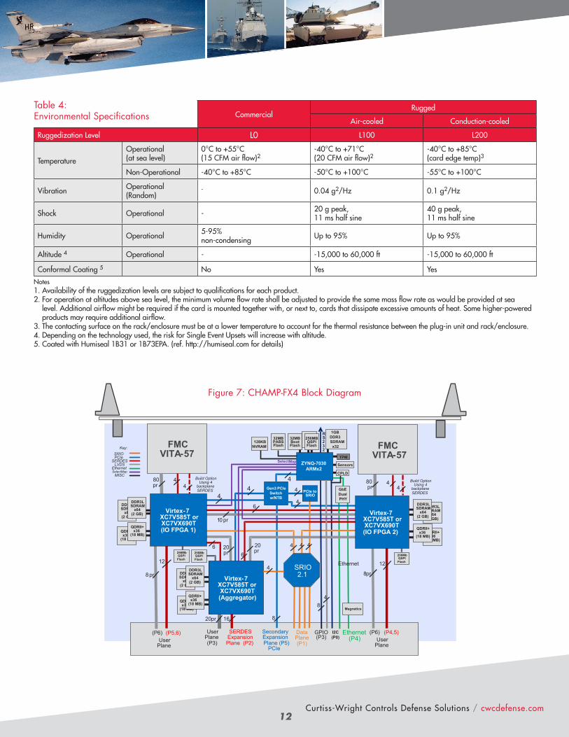
Table 4:Environmental Specifications Commercial
Rugged
Air-cooled Conduction-cooled
Ruggedization Level L0 L100 L200
Temperature
Operational (at sea level)
0°C to +55°C (15 CFM air flow)2
-40°C to +71°C (20 CFM air flow)2
-40°C to +85°C (card edge temp)3
Non-Operational -40°C to +85°C -50°C to +100°C -55°C to +100°C
Vibration Operational (Random)
- 0.04 g2/Hz 0.1 g2/Hz
Shock Operational - 20 g peak,11 ms half sine
40 g peak, 11 ms half sine
Humidity Operational 5-95% non-condensing Up to 95% Up to 95%
Altitude 4 Operational - -15,000 to 60,000 ft -15,000 to 60,000 ft
Conformal Coating 5 No Yes Yes
Notes1. Availability of the ruggedization levels are subject to qualifications for each product.2. For operation at altitudes above sea level, the minimum volume flow rate shall be adjusted to provide the same mass flow rate as would be provided at sea
level. Additional airflow might be required if the card is mounted together with, or next to, cards that dissipate excessive amounts of heat. Some higher-powered products may require additional airflow.
3. The contacting surface on the rack/enclosure must be at a lower temperature to account for the thermal resistance between the plug-in unit and rack/enclosure.4. Depending on the technology used, the risk for Single Event Upsets will increase with altitude.5. Coated with Humiseal 1B31 or 1B73EPA. (ref. http://humiseal.com for details)
Figure 7: CHAMP-FX4 Block Diagram

Curtiss-Wright Controls Defense Solutions / cwcdefense.com
© C
opyr
ight
201
3, C
urtis
s-Wrig
ht C
ontro
ls A
ll Ri
ghts
Rese
rved
. MKT
-DS-
CH
AM
P-FX
4-06
1213
v1
Warranty
This product has a one year warranty.
Contact Information
To find your appropriate sales representative:
Website: www.cwcdefense.com/sales
Email: [email protected]
Technical Support
For technical support:
Website: www.cwcdefense.com/support
Email: [email protected]
The information in this document is subject to change without notice and should not be construed as a commitment by Curtiss-Wright Controls Defense Solutions. While reasonable precautions have been taken, Curtiss-Wright assumes no responsibility for any errors that may appear in this document. All products shown or mentioned are trademarks or registered trademarks of their respective owners.
13
Part Numbers
Check with a Curtiss-Wright representative for availability of specific part numbers.
-E: to be added to indicate EAU models
Options
a: SERDES Option0 = IO-FPGA - x4 to FMC, x12 to backplane
= AGGR-FPGA - x16 with AC cap on RX1 = IO-FPGA - x4 to FMC, x12 to backplane
= AGGR-FPGA - x16 with AC cap on TX2 = IO-FPGA - x8 to FMC, x8 to backplane
= AGGR-FPGA - x16 with AC cap on RX3 = IO-FPGA - x8 to FMC, x8 to backplane
= AGGR-FPGA - x16 with AC cap on TX
b: QDR option0 = 18 MB parts1 = 36 MB parts
c: TPM0 = Unpopulated1 = Populated (ECCN 5A002)
FPGA 0 = 585T 1 = X690T 2 = 585T (-3C speed grade) L0 only 3 = X690T (-3C speed grade) L0 only
Mechanical Format: 4 = 1” pitch, no 2-level maintenance support 5 = 1” pitch, 2-level maintenance support (covers)
Temperature Range: 0 = 0 to 50°C 1 = -40 to 71°C 2 = -40 to 85°C
Cooling Method: A = Air-cooling C = Conduction-cooling
Model Number
Standard Prefix for 6U VPX cards
VPX6 - 473 - U V W X a b c [-E]