
Leakage Power Modelling and Minimization
43
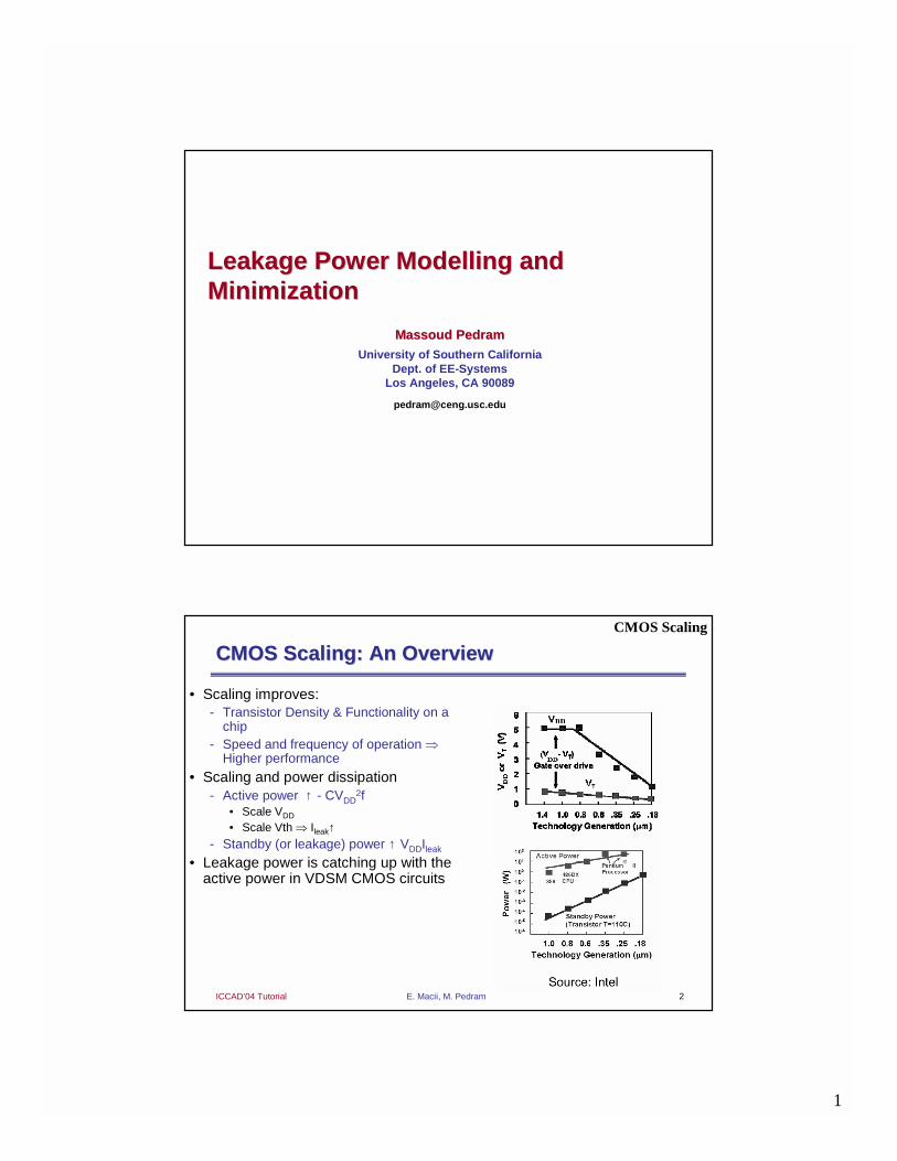
1 Leakage Power Modelling and Leakage Power Modelling and Minimization Minimization Massoud Pedram Massoud Pedram University of Southern California Dept. of EE-Systems Los Angeles, CA 90089 [email protected] 2 E. Macii, M. Pedram ICCAD’04 Tutorial CMOS Scaling: An Overview CMOS Scaling: An Overview • Scaling improves: - Transistor Density & Functionality on a chip - Speed and frequency of operation ⇒ Higher performance • Scaling and power dissipation - Active power ↑ - CV DD 2 f • Scale V DD • Scale Vth ⇒ I leak ↑ - Standby (or leakage) power ↑ V DD I leak • Leakage power is catching up with the active power in VDSM CMOS circuits CMOS Scaling
Transcript of Leakage Power Modelling and Minimization
1
Leakage Power Modelling and Leakage Power Modelling and MinimizationMinimization
Massoud PedramMassoud PedramUniversity of Southern California
Dept. of EE-SystemsLos Angeles, CA 90089
2E. Macii, M. PedramICCAD’04 Tutorial
CMOS Scaling: An OverviewCMOS Scaling: An Overview
• Scaling improves:- Transistor Density & Functionality on a
chip- Speed and frequency of operation ⇒
Higher performance
• Scaling and power dissipation- Active power ↑ - CVDD
2f• Scale VDD
• Scale Vth ⇒ Ileak↑- Standby (or leakage) power ↑ VDDIleak
• Leakage power is catching up with the active power in VDSM CMOS circuits
CMOS Scaling
2
3E. Macii, M. PedramICCAD’04 Tutorial
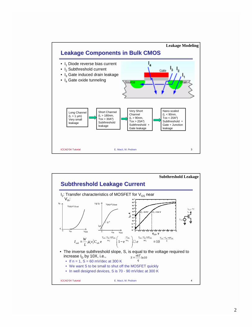
Leakage Components in Bulk CMOSLeakage Components in Bulk CMOS
• I1 Diode reverse bias current• I2 Subthreshold current • I3 Gate induced drain leakage • I4 Gate oxide tunneling
Long Channel (L > 1 µm) Very small leakage
Short Channel(L > 180nm, Tox > 30A0)Subthreshold leakage
Very Short Channel(L > 90nm, Tox > 20A0)Subthreshold +Gate leakage
Nano-scaled(L < 90nm, Tox < 20A0)Subthreshold +Gate + Junction leakage
Leakage Modeling
4E. Macii, M. PedramICCAD’04 Tutorial
Subthreshold Leakage CurrentSubthreshold Leakage Current
I2: Transfer characteristics of MOSFET for VGS near Vth:
10lnq
nkTS =
• The inverse subthreshold slope, S, is equal to the voltage required to increase ID by 10X, i.e., • If n = 1, S = 60 mV/dec at 300 K• We want S to be small to shut off the MOSFET quickly• In well designed devices, S is 70 - 90 mV/dec at 300 K
2 e 1 e 10GS th DS DS GS th DS GS th DS
T T T
V V V V V V V V V Vnv nv n S
sub e T sth
WI v C e
L
η η ηνµ
− + − − + − + = − ∝ =
Subthreshold Leakage
3
5E. Macii, M. PedramICCAD’04 Tutorial
Modeling Subthreshold (Modeling Subthreshold (IIsubsub) and ) and off (off (IIoffoff) Currents ) Currents • Increases exponentially with reduction in Vth
• Modulation of Vth in a short channel transistor- L ↓ ⇒ Vth ↓ : “Vth Rolloff”- VDS ↑ ⇒ Vth ↓ :”Drain Induced Barrier Lowering”- VSB ↑ ⇒ Vth ↑ : “Body Effect”
• If VDS = 0 ⇒ Isub = 0
• If VDS >> ⇒
• With
• Key dependencies of the subthreshold slope:- Tox ↓⇒ Cox ↑⇒ n ↓⇒ sharper subthreshold- NA ↑⇒ Csth ↑⇒ n ↑⇒ softer subthreshold- VSB ↑⇒ Csth ↓⇒ n ↓⇒ sharper subthreshold- T ↑⇒ softer subthreshold
2GS th
T
V V
nvsub e T sth
WI v C e
Lµ
−
=
1 12 2
sth
oxf
Cn
C
γ= + = +Φ
Tnv
T
th
nv
V
sthTeGSsuboff eCvL
WVII
−=== 2)0( µ
Subthreshold Leakage
• Occurs when transistor is “off”
6E. Macii, M. PedramICCAD’04 Tutorial
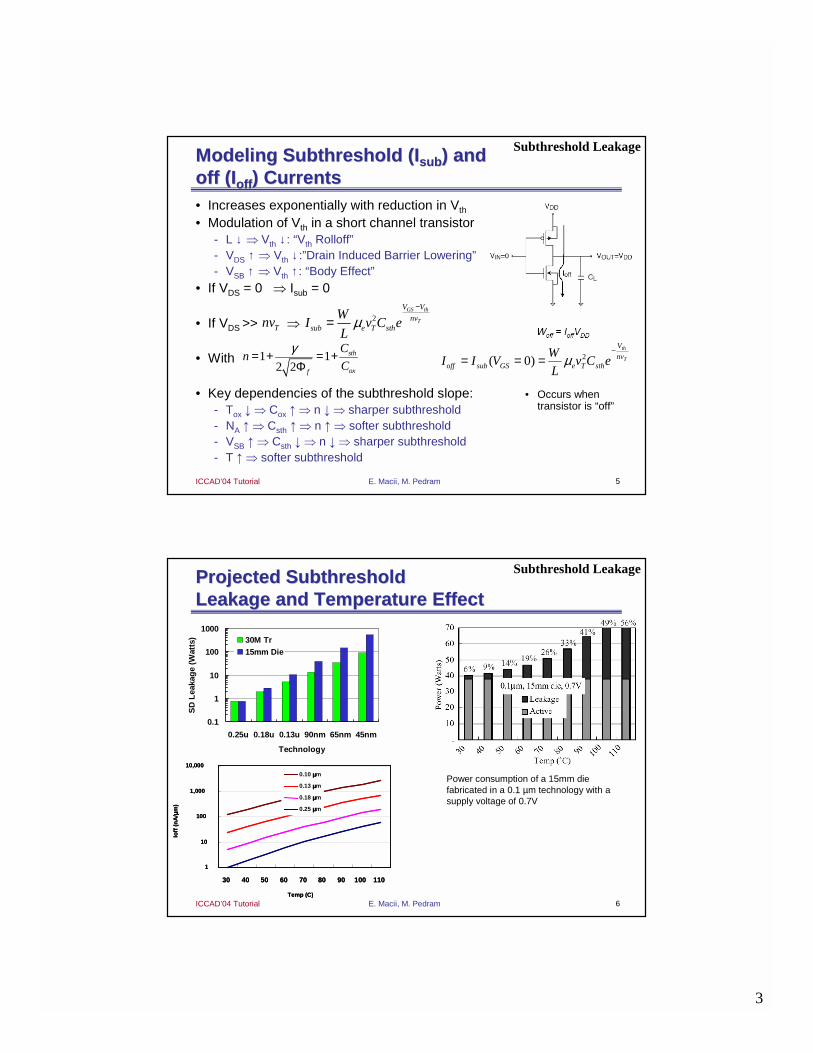
Projected Subthreshold Projected Subthreshold Leakage and Temperature EffectLeakage and Temperature Effect
0.1
1
10
100
1000
0.25u 0.18u 0.13u 90nm 65nm 45nm
Technology
SD
Lea
kag
e (W
atts
) 30M Tr15mm Die
Power consumption of a 15mm die fabricated in a 0.1 µm technology with a supply voltage of 0.7V
Subthreshold Leakage
1
10
100
1,000
10,000
30 40 50 60 70 80 90 100 110
Temp (C)
Ioff
(n
A/ µµ µµ
m)
0.10 µµµµm
0.13 µµµµm
0.18 µµµµm
0.25 µµµµm
1
10
100
1,000
10,000
30 40 50 60 70 80 90 100 110
Temp (C)
Ioff
(n
A/ µµ µµ
m)
0.10 µµµµm
0.13 µµµµm
0.18 µµµµm
0.25 µµµµm
4
7E. Macii, M. PedramICCAD’04 Tutorial
Gate Oxide TunnelingGate Oxide Tunneling
• I4: Gate oxide tunneling of electrons that can result in leakage when there is a high electric field across a thin gate oxide layer. Electrons may tunnel into the conduction band of the oxide layer; this is called Fowler-Nordheim tunneling
• In oxide layers less than 3–4 nm thick, there can also be direct tunneling through the silicon oxide layer. Mechanisms for directtunneling include electron tunneling in the conduction band (ECB), electron tunneling in the valence band (EVB), and hole tunneling in the valence band (HVB)
• Direct tunneling of electrons through gate oxide is the dominantsource. This current depends exponentially on the oxide thickness and the VDD [BSIM 4]
1.5
1 1
2( )
gsg
ox
gs
oxgs
ox
VB
V
TDT g
V
TJ A e
− − − Φ
=
Gate Leakage
• Occurs when transistor is “on”
8E. Macii, M. PedramICCAD’04 Tutorial
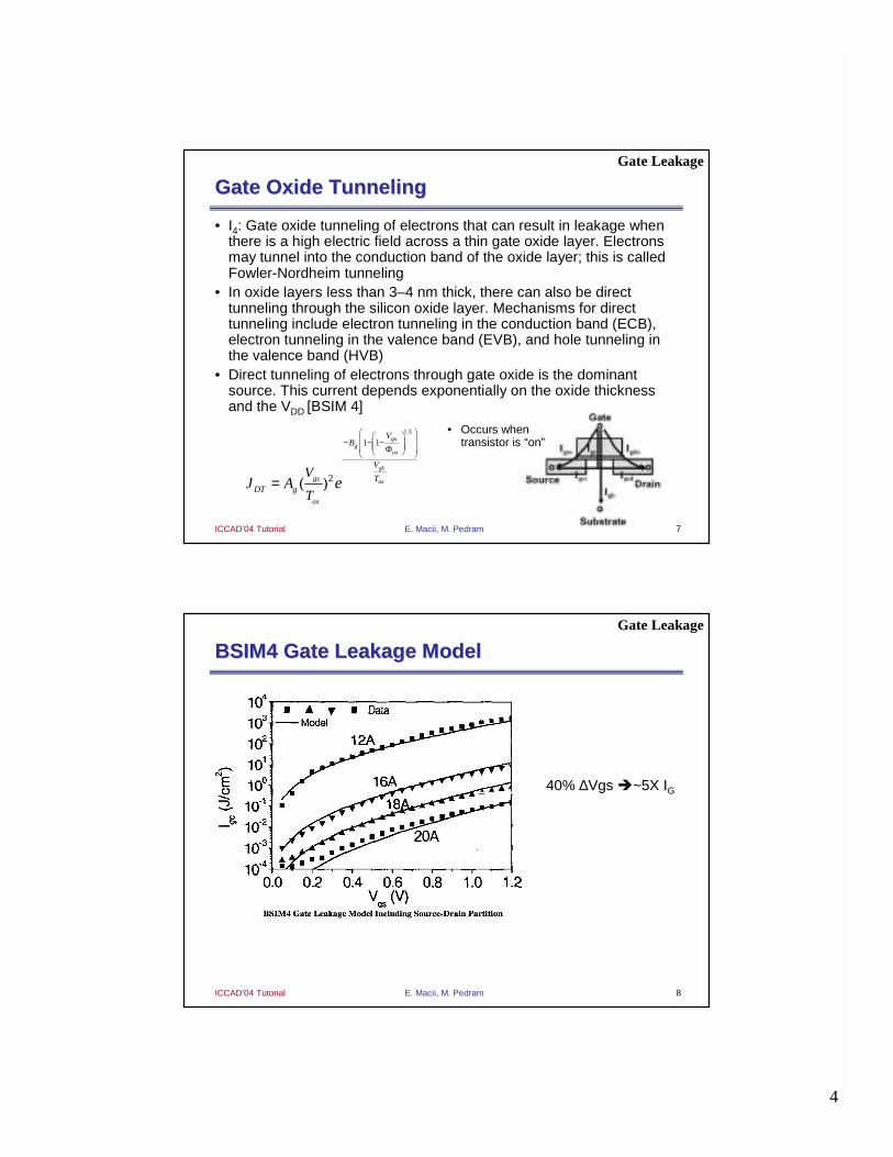
BSIM4 Gate Leakage ModelBSIM4 Gate Leakage Model
40% ∆Vgs !~5X IG
Gate Leakage
5
9E. Macii, M. PedramICCAD’04 Tutorial
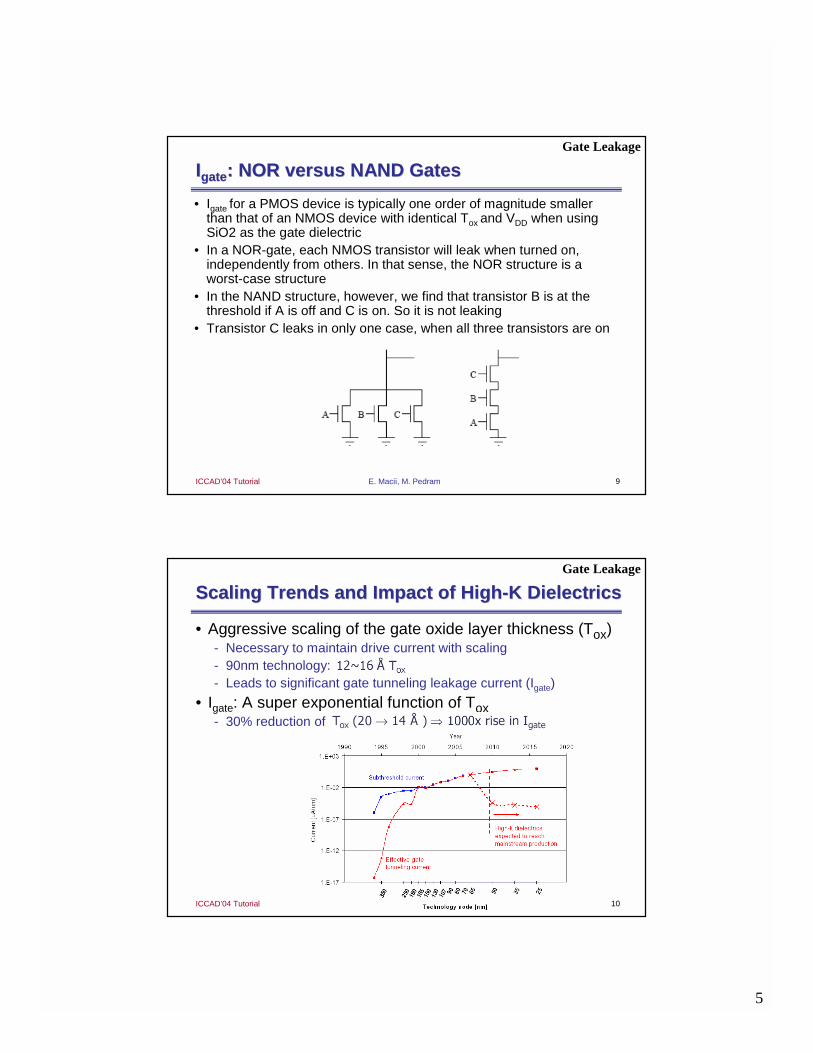
IIgategate: NOR versus NAND Gates: NOR versus NAND Gates
• Igate for a PMOS device is typically one order of magnitude smaller than that of an NMOS device with identical Tox and VDD when using SiO2 as the gate dielectric
• In a NOR-gate, each NMOS transistor will leak when turned on, independently from others. In that sense, the NOR structure is aworst-case structure
• In the NAND structure, however, we find that transistor B is at the threshold if A is off and C is on. So it is not leaking
• Transistor C leaks in only one case, when all three transistors are on
Gate Leakage
10E. Macii, M. PedramICCAD’04 Tutorial
Scaling Trends and Impact of HighScaling Trends and Impact of High--K DielectricsK Dielectrics
• Aggressive scaling of the gate oxide layer thickness (Tox)- Necessary to maintain drive current with scaling - 90nm technology: - Leads to significant gate tunneling leakage current (Igate)
• Igate: A super exponential function of Tox- 30% reduction of
Gate Leakage
6
11E. Macii, M. PedramICCAD’04 Tutorial
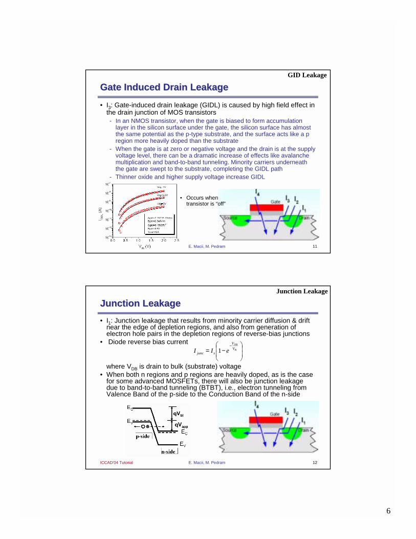
Gate Induced Drain LeakageGate Induced Drain Leakage
• I3: Gate-induced drain leakage (GIDL) is caused by high field effect in the drain junction of MOS transistors - In an NMOS transistor, when the gate is biased to form accumulation
layer in the silicon surface under the gate, the silicon surface has almost the same potential as the p-type substrate, and the surface acts like a p region more heavily doped than the substrate
- When the gate is at zero or negative voltage and the drain is at the supply voltage level, there can be a dramatic increase of effects like avalanche multiplication and band-to-band tunneling. Minority carriers underneath the gate are swept to the substrate, completing the GIDL path
- Thinner oxide and higher supply voltage increase GIDL
GID Leakage
• Occurs when transistor is “off”
12E. Macii, M. PedramICCAD’04 Tutorial
Junction LeakageJunction Leakage
• I1: Junction leakage that results from minority carrier diffusion & drift near the edge of depletion regions, and also from generation of electron hole pairs in the depletion regions of reverse-bias junctions
• Diode reverse bias current
where VDB is drain to bulk (substrate) voltage• When both n regions and p regions are heavily doped, as is the case
for some advanced MOSFETs, there will also be junction leakage due to band-to-band tunneling (BTBT), i.e., electron tunneling from Valence Band of the p-side to the Conduction Band of the n-side
−=
−th
DB
V
V
sjunc eII 1
Junction Leakage
7
13E. Macii, M. PedramICCAD’04 Tutorial
Leakage Reduction TechniquesLeakage Reduction Techniques
• Lowering Vdd (voltage islands, dynamic voltage scaling)• SOI technology• Cooling and/or refrigeration• Gate-level dual-Vth design • Mixed-Vth (MVT) CMOS design • Transistor sizing (shorter W, longer L)• Transistor stacking• Body bias control (static and/or adaptive)• Input vector control during sleep mode• MTCMOS (sleep transistors, power gating)
Leakage Reduction
14E. Macii, M. PedramICCAD’04 Tutorial
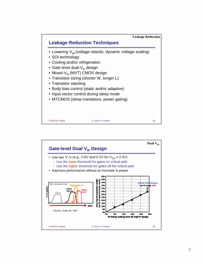
GateGate--level Dual level Dual VVthth DesignDesign
• Use two- Use the lower threshold for gates on critical path- Use the higher threshold for gates off the critical path
• Improves performance without an increase in power
Dual Vth
# o
f p
ath
s
slack
150nm
100nm high-Vt 100nm
low-Vt
100nm dual-- VtNote: not drawn to scale
# o
f p
ath
s
slack
150nm
100nm high-Vt 100nm
low-Vt
100nm dual-- VtNote: not drawn to scale
0%
5%
10%
15%
20%
25%
30%
35%
40%
45%
50%
55%
60%
0% 5% 10% 15% 20% 25%
% timing scaling from all high-Vt design
very
low
- Vt
tran
sist
or
wid
th(a
s %
of t
otal
tran
sist
or w
idth
)
0%
5%
10%
15%
20%
25%
30%
35%
40%
45%
50%
55%
60%
0% 5% 10% 15% 20% 25%
% timing scaling from all high-Vt design
very
low
- Vt
tran
sist
or
wid
th(a
s %
of t
otal
tran
sist
or w
idth
)
Full low-Vt performance!low-Vt usage: 34%
0%
5%
10%
15%
20%
25%
30%
35%
40%
45%
50%
55%
60%
0% 5% 10% 15% 20% 25%
% timing scaling from all high-Vt design
very
low
- Vt
tran
sist
or
wid
th(a
s %
of t
otal
tran
sist
or w
idth
)
0%
5%
10%
15%
20%
25%
30%
35%
40%
45%
50%
55%
60%
0% 5% 10% 15% 20% 25%
% timing scaling from all high-Vt design
very
low
- Vt
tran
sist
or
wid
th(a
s %
of t
otal
tran
sist
or w
idth
)
Full low-Vt performance!low-Vt usage: 34%
Source: Vivek De, Intel
8
15E. Macii, M. PedramICCAD’04 Tutorial
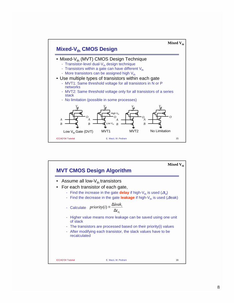
MixedMixed--VVthth CMOS DesignCMOS Design
• Mixed-Vth (MVT) CMOS Design Technique- Transistor-level dual-Vth design technique- Transistors within a gate can have different Vth
- More transistors can be assigned high Vth
• Use multiple types of transistors within each gate - MVT1: Same threshold voltage for all transistors in N or P
networks- MVT2: Same threshold voltage only for all transistors of a series
stack - No limitation (possible in some processes)
Vdd
A
B
O O
Vdd
A
B
Low Vth Gate (DVT) MVT1
O
Vdd
A
B
No Limitation
O
Vdd
A
B
MVT2
Mixed Vth
Low Vth
High Vth
16E. Macii, M. PedramICCAD’04 Tutorial
MVT CMOS Design AlgorithmMVT CMOS Design Algorithm
• Assume all low-Vth transistors• For each transistor of each gate,
- Find the increase in the gate delay if high-Vth is used (∆td)- Find the decrease in the gate leakage if high-Vth is used (∆leak)
- Calculate
- Higher value means more leakage can be saved using one unit of slack
- The transistors are processed based on their priority(i) values- After modifying each transistor, the slack values have to be
recalculated
id
i
t
leakipriority
∆∆=)(
Mixed Vth
9
17E. Macii, M. PedramICCAD’04 Tutorial
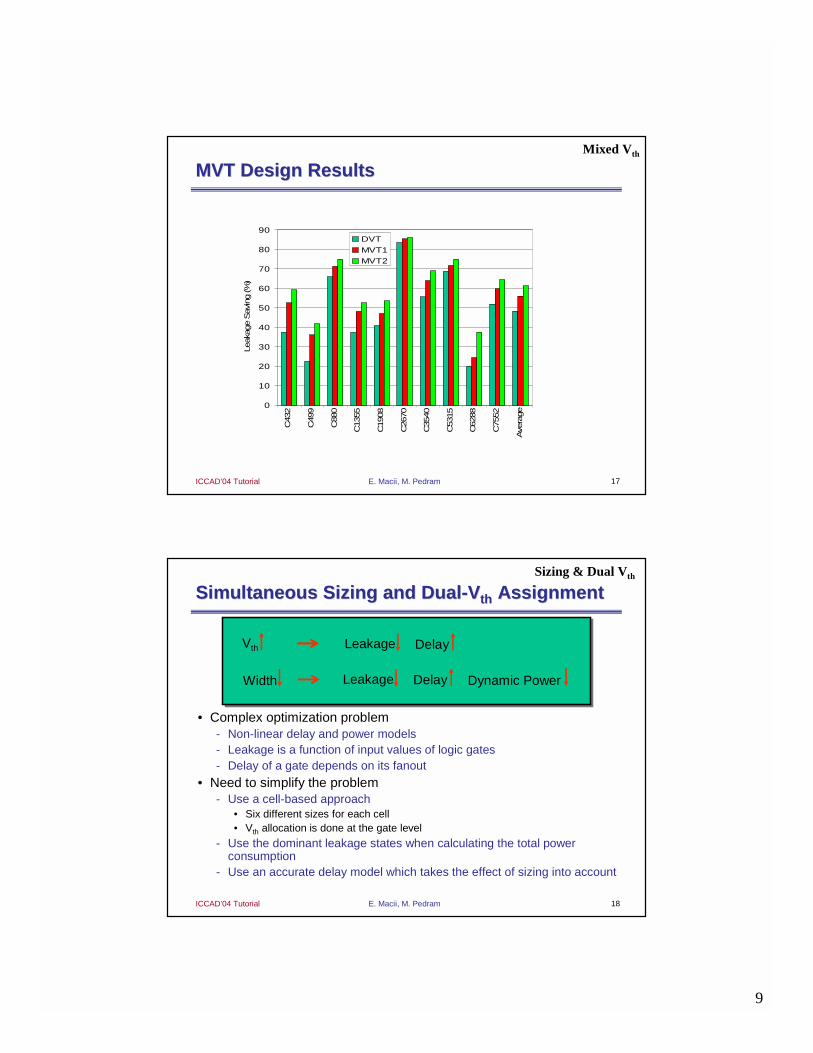
MVT Design ResultsMVT Design Results
0
10
20
30
40
50
60
70
80
90
C432
C499
C880
C1355
C1908
C2670
C3540
C5315
C6288
C7552
Ave
rage
Leaka
ge S
avi
ng (%
)DVTMVT1MVT2
Mixed Vth
18E. Macii, M. PedramICCAD’04 Tutorial
Simultaneous Sizing and DualSimultaneous Sizing and Dual--VVthth AssignmentAssignment
• Complex optimization problem- Non-linear delay and power models - Leakage is a function of input values of logic gates- Delay of a gate depends on its fanout
• Need to simplify the problem- Use a cell-based approach
• Six different sizes for each cell• Vth allocation is done at the gate level
- Use the dominant leakage states when calculating the total powerconsumption
- Use an accurate delay model which takes the effect of sizing into account
Sizing & Dual Vth
Vth DelayLeakage
Width Dynamic PowerDelayLeakage
10
19E. Macii, M. PedramICCAD’04 Tutorial
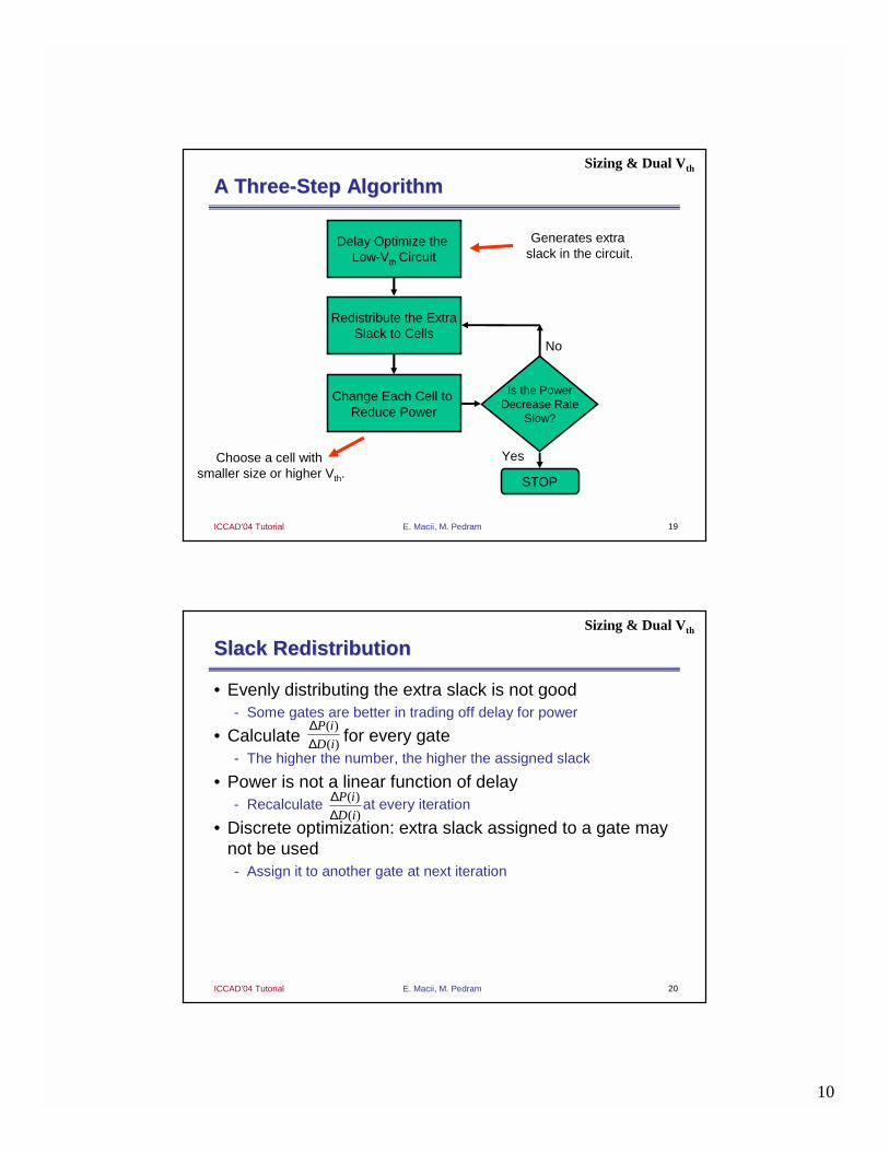
A ThreeA Three--Step AlgorithmStep AlgorithmSizing & Dual Vth
Delay Optimize the Low-Vth Circuit
Redistribute the ExtraSlack to Cells
Generates extra slack in the circuit.
Change Each Cell to Reduce Power
Is the PowerDecrease Rate
Slow?
No
Yes
STOP
Choose a cell with smaller size or higher Vth.
20E. Macii, M. PedramICCAD’04 Tutorial
Slack RedistributionSlack Redistribution
• Evenly distributing the extra slack is not good- Some gates are better in trading off delay for power
• Calculate for every gate- The higher the number, the higher the assigned slack
• Power is not a linear function of delay- Recalculate at every iteration
• Discrete optimization: extra slack assigned to a gate may not be used- Assign it to another gate at next iteration
Sizing & Dual Vth
)(
)(
iD
iP
∆∆
)(
)(
iD
iP
∆∆
11
21E. Macii, M. PedramICCAD’04 Tutorial
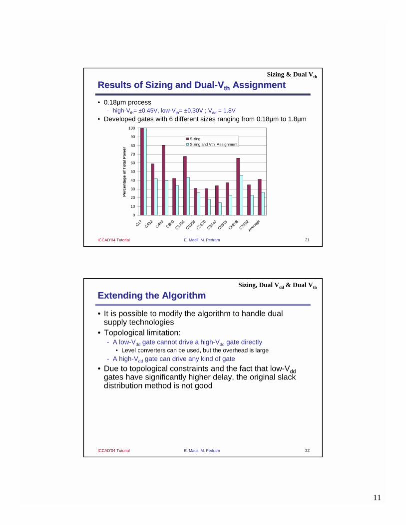
Results of Sizing and DualResults of Sizing and Dual--VVthth AssignmentAssignment
• 0.18µm process- high-Vth= ±0.45V, low-Vth= ±0.30V ; Vdd = 1.8V
• Developed gates with 6 different sizes ranging from 0.18µm to 1.8µm
Sizing & Dual Vth
0
10
20
30
40
50
60
70
80
90
100
C17C43
2C49
9C88
0
C1355
C1908
C2670
C3540
C5315
C6288
C7552
Avera
ge
Per
cen
tag
e o
f To
tal P
ow
er
SizingSizing and Vth Assignment
22E. Macii, M. PedramICCAD’04 Tutorial
Extending the AlgorithmExtending the Algorithm
• It is possible to modify the algorithm to handle dual supply technologies
• Topological limitation:- A low-Vdd gate cannot drive a high-Vdd gate directly
• Level converters can be used, but the overhead is large
- A high-Vdd gate can drive any kind of gate
• Due to topological constraints and the fact that low-Vddgates have significantly higher delay, the original slack distribution method is not good
Sizing, Dual Vdd & Dual Vth
12
23E. Macii, M. PedramICCAD’04 Tutorial
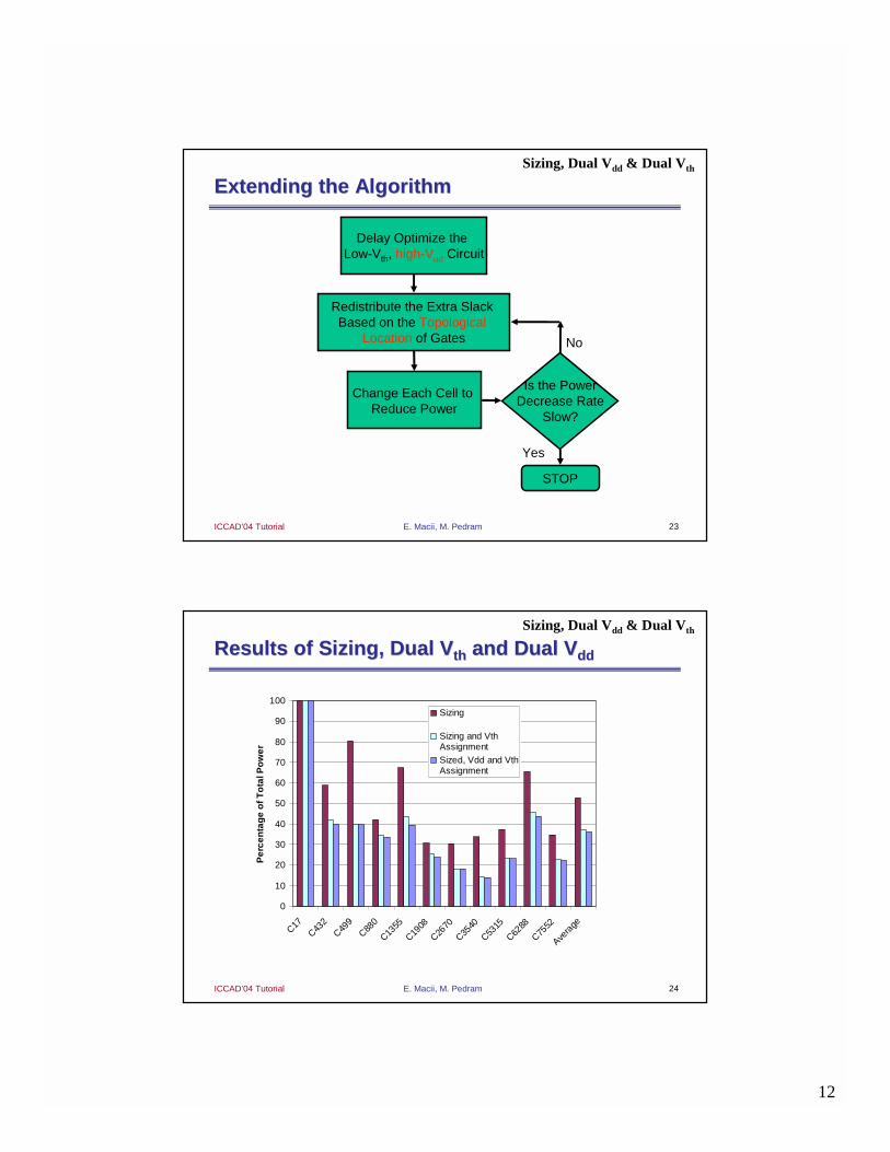
Extending the AlgorithmExtending the AlgorithmSizing, Dual Vdd & Dual Vth
Delay Optimize the Low-Vth, high-Vdd Circuit
Redistribute the Extra Slack Based on the Topological
Location of Gates
Change Each Cell to Reduce Power
Is the PowerDecrease Rate
Slow?
No
Yes
STOP
24E. Macii, M. PedramICCAD’04 Tutorial
Results of Sizing, Dual Results of Sizing, Dual VVthth and Dual and Dual VVdddd
Sizing, Dual Vdd & Dual Vth
0
10
20
30
40
50
60
70
80
90
100
C17C43
2C49
9C88
0
C1355
C1908
C2670
C3540
C5315
C6288
C7552
Avera
ge
Per
cen
tag
e o
f To
tal P
ow
er
Sizing
Sizing and VthAssignmentSized, Vdd and VthAssignment
13
25E. Macii, M. PedramICCAD’04 Tutorial
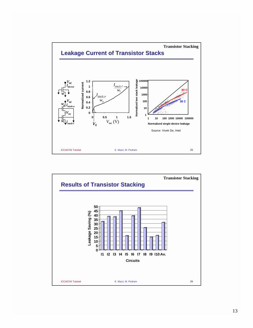
Leakage Current of Transistor StacksLeakage Current of Transistor StacksTransistor Stacking
0
0.2
0.4
0.6
0.8
1
1.2
0 0.5 1 1.5Vint (V)
Nor
mal
ized
cur
rent
VX
Istack-l
wl
Istack-u
wu
Vint (V)
0
0.2
0.4
0.6
0.8
1
1.2
0 0.5 1 1.5Vint (V)
Nor
mal
ized
cu
rren
t
V
Istack-l
wl
Istack-u
wu
Vint (V)
0
0.2
0.4
0.6
0.8
1
1.2
0 0.5 1 1.5Vint (V)
Nor
mal
ized
cur
rent
0
0.2
0.4
0.6
0.8
1
1.2
0 0.5 1 1.5Vint (V)
Nor
mal
ized
cur
rent
VX
Istack-l
wl
Istack-u
wu
Vint (V)
0
0.2
0.4
0.6
0.8
1
1.2
0 0.5 1 1.5Vint (V)
Nor
mal
ized
cu
rren
t
V
Istack-l
wl
Istack-u
wu
Vint (V)
VddIdevice
w
VddIdevice
w
Vdd
Istack-u
Vint
wu
wl Istack-l
Vdd
Istack-u
Vint
wu
wl Istack-l
1
10
100
1000
10000
100000
1 10 100 1000 10000 100000
Normalized single device leakage
Nor
mal
ize
d tw
o s
tack
leak
age 30OC and 80OC
1
10
100
1000
10000
100000
1 10 100 1000 10000 100000
Normalized single device leakage
Nor
mal
ize
d tw
o s
tack
leak
age
1
10
100
1000
10000
100000
1 10 100 1000 10000 100000
Normalized single device leakage
No
rmal
ized
tw
o s
tack
leak
age
30OC and 80OC
1
10
100
1000
10000
100000
1 10 100 1000 10000 100000
Normalized single device leakage
Nor
mal
ize
d tw
o s
tack
leak
age
1
10
100
1000
10000
100000
1 10 100 1000 10000 100000
Normalized single device leakage
Nor
mal
ize
d tw
o s
tack
leak
age
1
10
100
1000
10000
100000
1 10 100 1000 10000 100000
Normalized single device leakage
Nor
mal
ize
d tw
o s
tack
leak
age 30OC and 80OC
1
10
100
1000
10000
100000
1 10 100 1000 10000 100000
Normalized single device leakage
Nor
mal
ize
d tw
o s
tack
leak
age
1
10
100
1000
10000
100000
1 10 100 1000 10000 100000
Normalized single device leakage
Nor
mal
ize
d tw
o s
tack
leak
age
1
10
100
1000
10000
100000
1 10 100 1000 10000 100000
Normalized single device leakage
No
rmal
ized
tw
o s
tack
leak
age
30OC and 80OC
80 C
30 C
Source: Vivek De, Intel
26E. Macii, M. PedramICCAD’04 Tutorial
Results of Transistor StackingResults of Transistor Stacking
05
101520253035404550
Lea
kag
e S
avin
g (
%)
I1 I2 I3 I4 I5 I6 I7 I8 I9 I10 Av.
Circuits
Transistor Stacking
14
27E. Macii, M. PedramICCAD’04 Tutorial
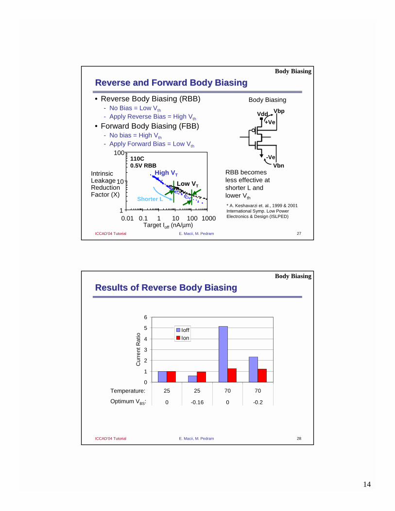
Reverse and Forward Body BiasingReverse and Forward Body Biasing
Body Biasing
Vdd Vbp
Vbn-Ve
+Ve
Body Biasing
• Reverse Body Biasing (RBB)- No Bias = Low Vth
- Apply Reverse Bias = High Vth
• Forward Body Biasing (FBB)- No bias = High Vth
- Apply Forward Bias = Low Vth
1
10
100
0.01 0.1 1 10 100 1000Target Ioff (nA/µm)
110C0.5V RBB
Low VT
High VTIntrinsicLeakageReductionFactor (X)
Shorter L
RBB becomes less effective at shorter L and lower Vth
* A. Keshavarzi et. al., 1999 & 2001 International Symp. Low Power Electronics & Design (ISLPED)
28E. Macii, M. PedramICCAD’04 Tutorial
Results of Reverse Body BiasingResults of Reverse Body BiasingBody Biasing
0
1
2
3
4
5
6
25 25 70 70
0 -0.16 0 -0.2
Cur
rent
Rat
io
IoffIon
Temperature:
Optimum VBS:

15
29E. Macii, M. PedramICCAD’04 Tutorial
Input Dependence of the Leakage CurrentInput Dependence of the Leakage Current
Technology: 0.18 Technology: 0.18 µµmmSupply Voltage = 1.5VSupply Voltage = 1.5VThreshold VoltageThreshold Voltage = 0.2V= 0.2V
X0 X1X0 X1 LeakageLeakage
0 00 0 23.60 nA23.60 nA
51.42 nA51.42 nA
47.15 nA47.15 nA
82.94 nA82.94 nA
X0
X1
X0
X1
0 10 1
1 01 0
1 11 1
Input Vector Control
30E. Macii, M. PedramICCAD’04 Tutorial
Input Vector Control During Sleep ModeInput Vector Control During Sleep Mode
0
1
Combinational Logic
Primary Inputs
Min-Leakage Vector
sleep
sleepinput
input’
Min-Leakage Input = 0
sleep input’
0 input
1 0
sleepinput
input’
Min-Leakage Input = 1
sleep input’
0 input
1 1
Input Vector Control
16
31E. Macii, M. PedramICCAD’04 Tutorial
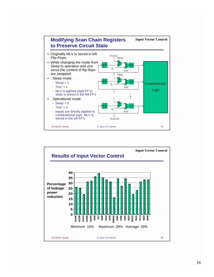
Modifying Scan Chain Registers Modifying Scan Chain Registers to Preserve Circuit Stateto Preserve Circuit State
• Originally MLV is stored in left Flip-Flops.
• While changing the mode from Sleep to operation and vice versa the content of flip-flops are swapped.
• . Sleep mode:- Sleep = 1- Test’ = 1- MLV is applied (right FF’s);
State is stored in the left FF’s
• . Operational mode:- Sleep = 0- Test’ = 0- Inputs are directly applied to
combinational logic; MLV is stored in the left FF’s
FF10
Combinational
Logic...
Test’
Scan In
Scan Out
01
Sleep
FF10
Test’
01
Sleep
in1
in2
FF
FF
FF10
Test’
01
inn
FF
Input Vector Control
32E. Macii, M. PedramICCAD’04 Tutorial
Results of Input Vector ControlResults of Input Vector Control
Minimum: 16% Maximum: 39% Average: 29%
0
5
10
15
20
25
30
35
40
S11
96
S12
38
S14
23
S14
88
S14
94
S20
8
S27
S29
8
S34
4
S34
9
S35
932
S38
2
S38
6
S40
0
S51
0
S53
78
S64
1
S71
3
S82
0
S83
8
Input Vector Control
Percentage of leakage power reduction
17
33E. Macii, M. PedramICCAD’04 Tutorial
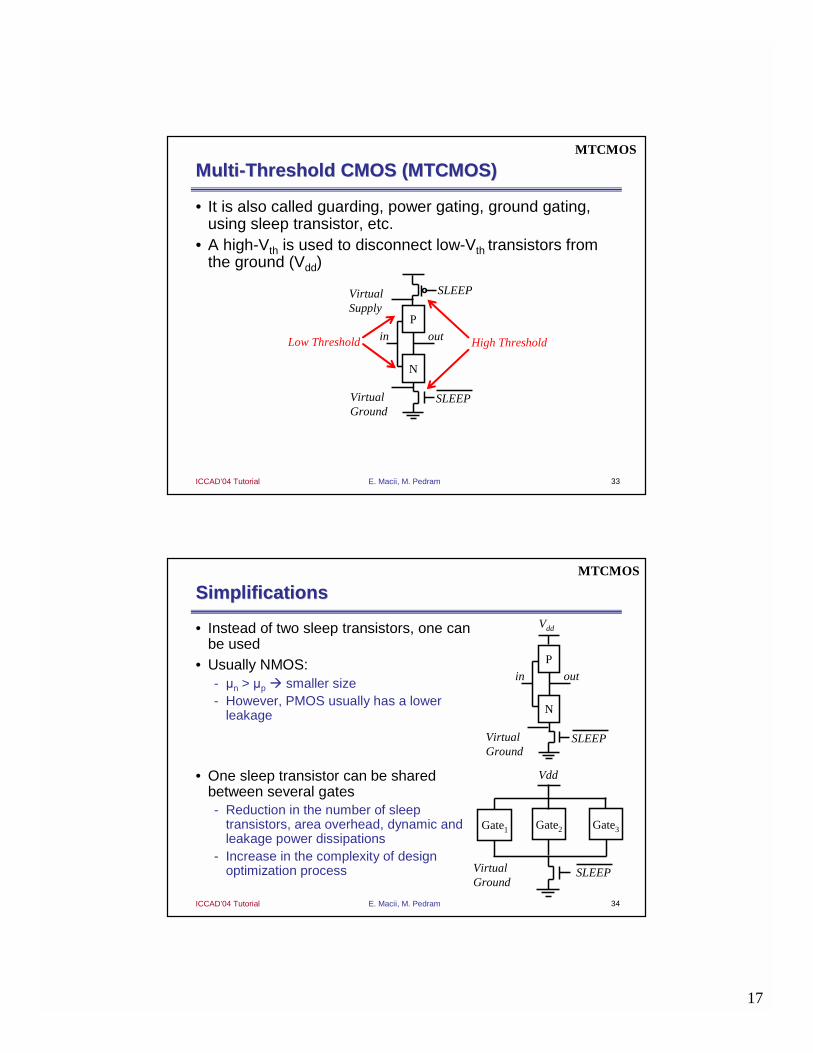
MultiMulti--Threshold CMOS (MTCMOS)Threshold CMOS (MTCMOS)
• It is also called guarding, power gating, ground gating, using sleep transistor, etc.
• A high-Vth is used to disconnect low-Vth transistors from the ground (Vdd)
MTCMOS
N
outin
SLEEP
P
SLEEP
Virtual Supply
Virtual Ground
Low Threshold High Threshold
34E. Macii, M. PedramICCAD’04 Tutorial
SimplificationsSimplifications
• Instead of two sleep transistors, one can be used
• Usually NMOS:- µn > µp " smaller size- However, PMOS usually has a lower
leakage
• One sleep transistor can be shared between several gates- Reduction in the number of sleep
transistors, area overhead, dynamic and leakage power dissipations
- Increase in the complexity of design optimization process
N
outin
P
SLEEPVirtual Ground
Vdd
MTCMOS
Gate1
SLEEPVirtual Ground
Gate2 Gate3
Vdd
18
35E. Macii, M. PedramICCAD’04 Tutorial
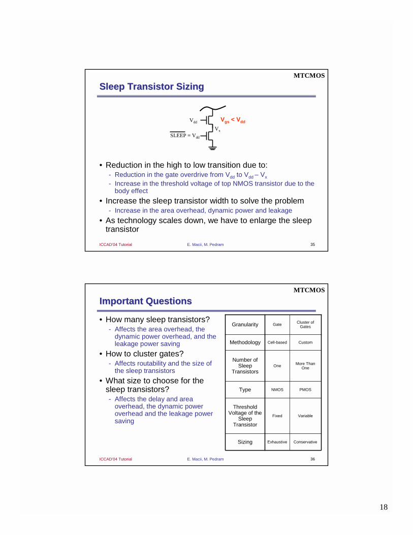
Sleep Transistor SizingSleep Transistor Sizing
• Reduction in the high to low transition due to:- Reduction in the gate overdrive from Vdd to Vdd – Vx
- Increase in the threshold voltage of top NMOS transistor due to the body effect
• Increase the sleep transistor width to solve the problem- Increase in the area overhead, dynamic power and leakage
• As technology scales down, we have to enlarge the sleep transistor
SLEEP = Vdd
Vx
Vdd Vgs < Vdd
MTCMOS
36E. Macii, M. PedramICCAD’04 Tutorial
Important QuestionsImportant Questions
• How many sleep transistors?- Affects the area overhead, the
dynamic power overhead, and the leakage power saving
• How to cluster gates?- Affects routability and the size of
the sleep transistors
• What size to choose for the sleep transistors?- Affects the delay and area
overhead, the dynamic power overhead and the leakage power saving
VariableFixed
Threshold Voltage of the
Sleep Transistor
PMOSNMOSType
More Than OneOne
Number of Sleep
Transistors
CustomCell-basedMethodology
ConservativeExhaustiveSizing
Cluster of GatesGateGranularity
MTCMOS
19
37E. Macii, M. PedramICCAD’04 Tutorial
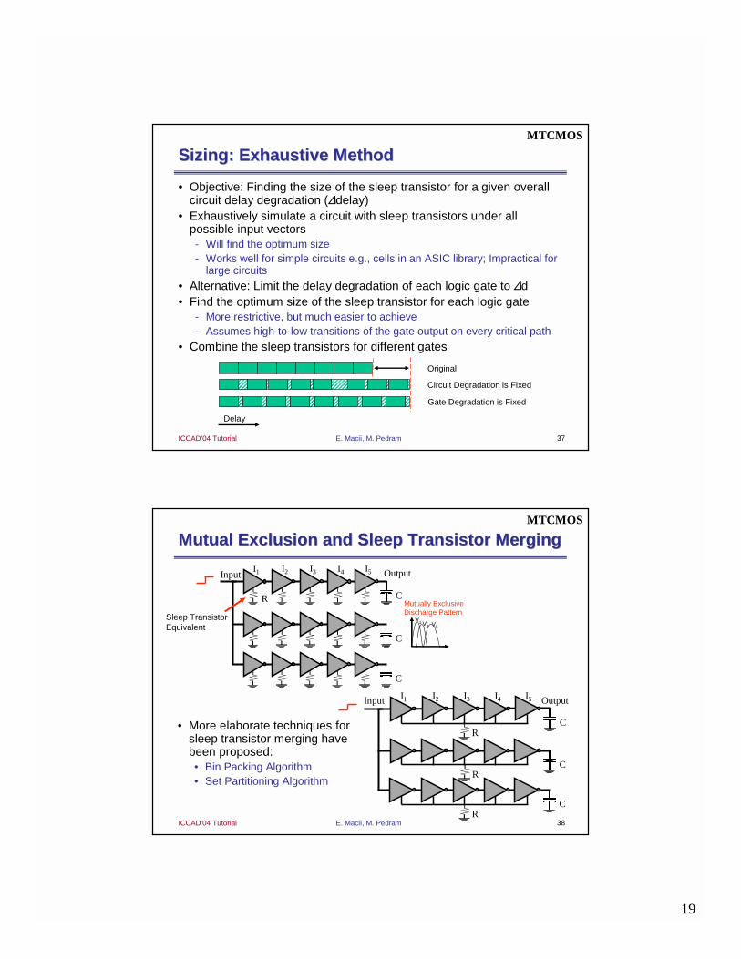
Sizing: Exhaustive MethodSizing: Exhaustive Method
• Objective: Finding the size of the sleep transistor for a given overallcircuit delay degradation (∆delay)
• Exhaustively simulate a circuit with sleep transistors under allpossible input vectors- Will find the optimum size- Works well for simple circuits e.g., cells in an ASIC library; Impractical for
large circuits
• Alternative: Limit the delay degradation of each logic gate to ∆d• Find the optimum size of the sleep transistor for each logic gate
- More restrictive, but much easier to achieve- Assumes high-to-low transitions of the gate output on every critical path
• Combine the sleep transistors for different gates
MTCMOS
Delay
Original
Circuit Degradation is Fixed
Gate Degradation is Fixed
38E. Macii, M. PedramICCAD’04 Tutorial
Mutual Exclusion and Sleep Transistor MergingMutual Exclusion and Sleep Transistor MergingMTCMOS
C
I1 I2 I3 I4 I5
C
OutputInput
C
R
V1 V3 V5
Mutually ExclusiveDischarge Pattern
Sleep TransistorEquivalent
C
I1 I2 I3 I4 I5
C
OutputInput
C
R
R
R
• More elaborate techniques for sleep transistor merging have been proposed:• Bin Packing Algorithm• Set Partitioning Algorithm
20
39E. Macii, M. PedramICCAD’04 Tutorial
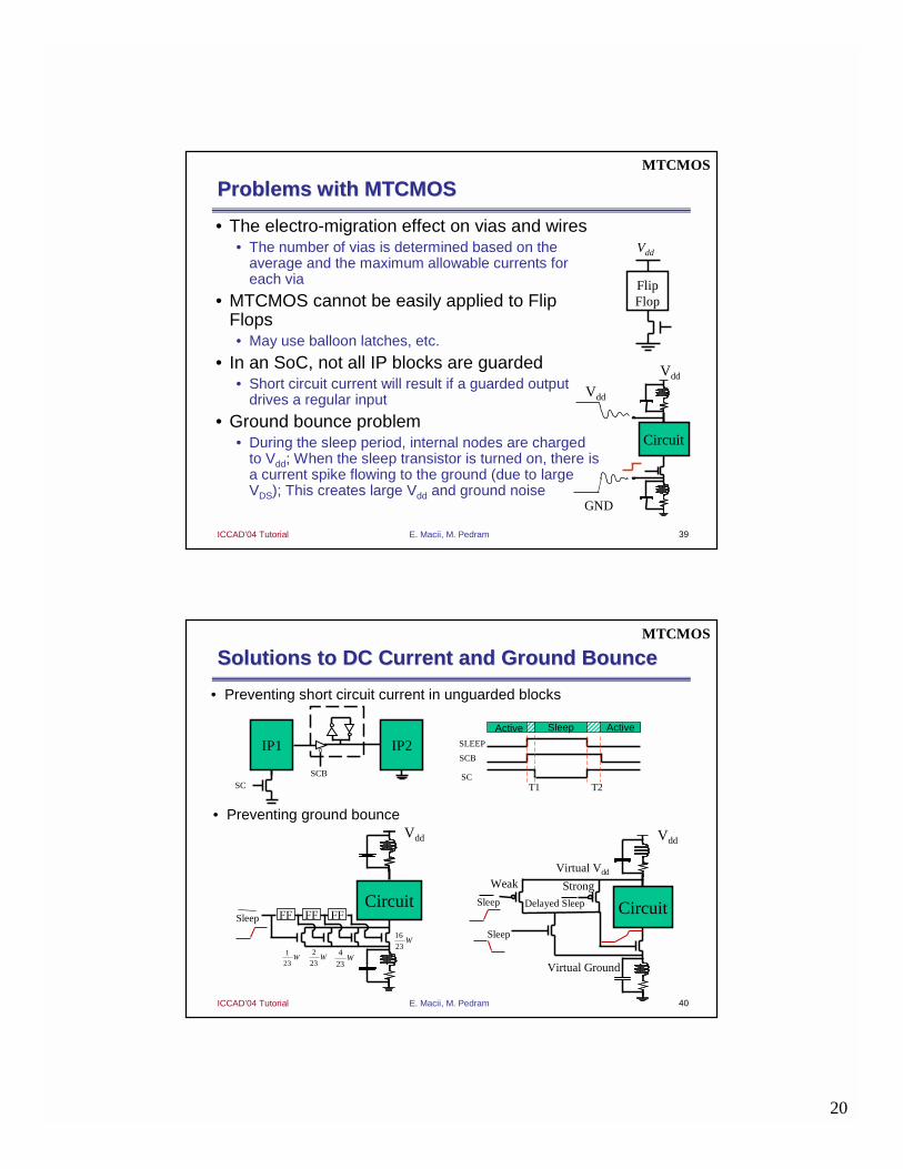
Problems with MTCMOSProblems with MTCMOS
• The electro-migration effect on vias and wires• The number of vias is determined based on the
average and the maximum allowable currents for each via
• MTCMOS cannot be easily applied to Flip Flops• May use balloon latches, etc.
• In an SoC, not all IP blocks are guarded • Short circuit current will result if a guarded output
drives a regular input
• Ground bounce problem• During the sleep period, internal nodes are charged
to Vdd; When the sleep transistor is turned on, there is a current spike flowing to the ground (due to large VDS); This creates large Vdd and ground noise
Flip Flop
Vdd
MTCMOS
Circuit
Vdd
Vdd
GND
40E. Macii, M. PedramICCAD’04 Tutorial
Solutions to DC Current and Ground BounceSolutions to DC Current and Ground Bounce
Active ActiveSleep
T1 T2SC
SCB
SLEEP
• Preventing ground bounce
• Preventing short circuit current in unguarded blocks
MTCMOS
Circuit
Vdd
Sleep FFFFFF
W23
1W
23
2W
23
4
W23
16
Circuit
Virtual Ground
Vdd
Virtual Vdd
Weak
Sleep
Sleep Delayed Sleep
Strong
SC
IP2
SCB
IP1
21
41E. Macii, M. PedramICCAD’04 Tutorial
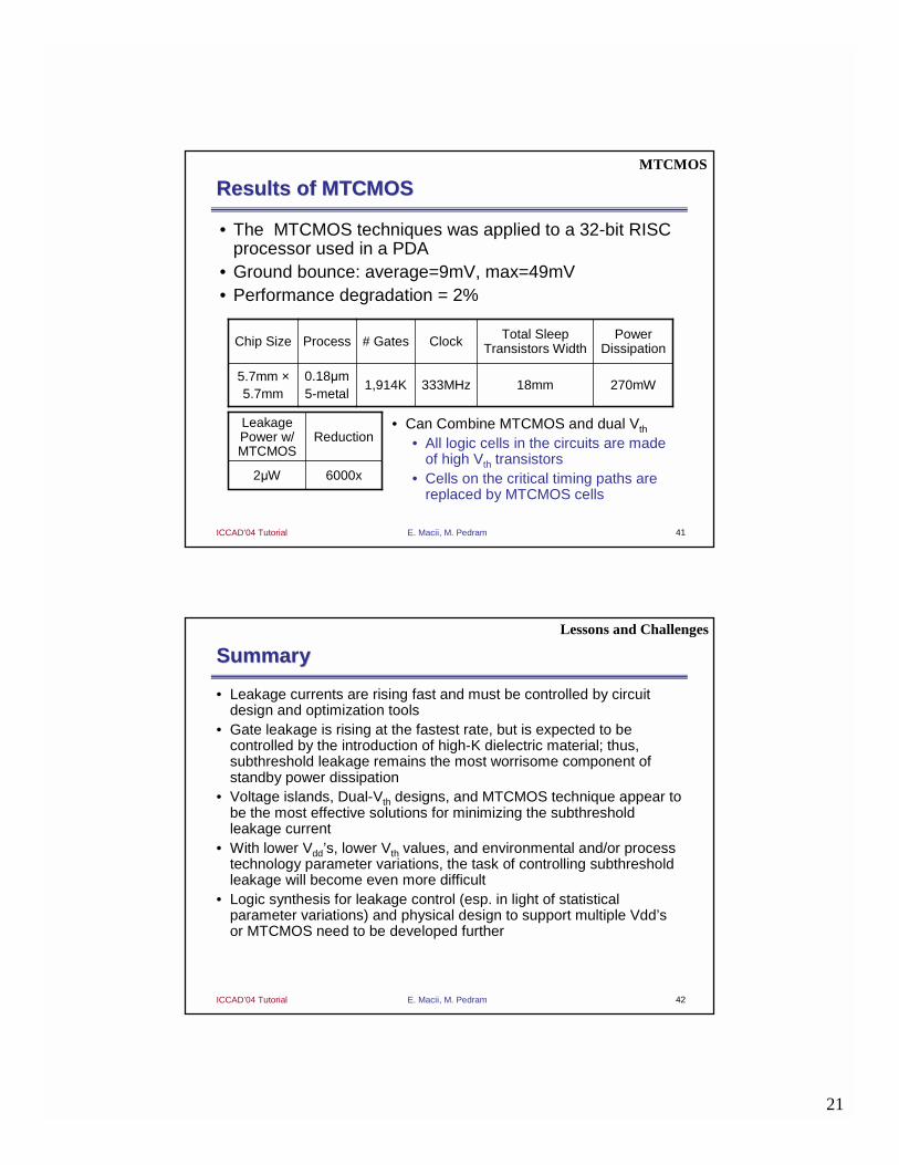
Results of MTCMOSResults of MTCMOS
333MHz
Clock
1,914K
# Gates
0.18µm 5-metal
Process
270mW18mm5.7mm ×5.7mm
Power Dissipation
Total Sleep Transistors WidthChip Size
MTCMOS
• The MTCMOS techniques was applied to a 32-bit RISC processor used in a PDA
• Ground bounce: average=9mV, max=49mV• Performance degradation = 2%
6000x2µW
ReductionLeakage Power w/ MTCMOS
• Can Combine MTCMOS and dual Vth
• All logic cells in the circuits are made of high Vth transistors
• Cells on the critical timing paths are replaced by MTCMOS cells
42E. Macii, M. PedramICCAD’04 Tutorial
SummarySummary
• Leakage currents are rising fast and must be controlled by circuit design and optimization tools
• Gate leakage is rising at the fastest rate, but is expected to be controlled by the introduction of high-K dielectric material; thus, subthreshold leakage remains the most worrisome component of standby power dissipation
• Voltage islands, Dual-Vth designs, and MTCMOS technique appear to be the most effective solutions for minimizing the subthreshold leakage current
• With lower Vdd’s, lower Vth values, and environmental and/or process technology parameter variations, the task of controlling subthreshold leakage will become even more difficult
• Logic synthesis for leakage control (esp. in light of statistical parameter variations) and physical design to support multiple Vdd’sor MTCMOS need to be developed further
Lessons and Challenges
22
43E. Macii, M. PedramICCAD’04 Tutorial
ReferencesReferences
• M. Pedram, “Power minimization in IC design: principles and applications,” invited paper, ACM Transactions on Design Automation of Electronic Systems, Vol. 1, No. 1, 1996, pp. 3-56.
• V. De and S. Borkar, “Technology and design challenges for low power and high performance,” in Proc. Int. Symp. Low Power Electronics and Design, 1999, pp. 163–168.
• A. Keshavarzi, K. Roy, and C. F. Hawkins, “Intrinsic leakage in low power deep submicron CMOS ics,” in Proc. Int. Test Conf., 1997, pp. 146–155.
• V. De, Y. Ye, A. Keshavarzi, S. Narendra, J. Kao, D. Somasekhar, R. Nair, and S. Borkar, “Techniques for leakage power reduction,” in Design of High-Performance Microprocessor Circuits, A. Chandrakasan, W. Bowhill, and F. Fox, Eds. Piscataway, NJ: IEEE, 2001, ch. 3, pp. 48–52.
• K. Cao,W.-C Lee,W. Liu, X. Jin, P. Su, S. Fung, J. An, B. Yu, and C. Hu, “BSIM4 gate leakage model including source drain partition,” in Tech. Dig. Int. Electron Devices Meeting, 2000, pp. 815–818.
• F. Hamzaoglu and M. Stan, “Circuit-level techniques to control gate leakage for sub-100 nm CMOS,” in Proc. Int. Symp. Low Power Design, 2002, pp. 60–63.
• N. Yang, W. Henson, and J. Hauser, “Modeling study of ultra-thin gate oxides using tunneling current and capacitance-voltage measurement in MOS Devices,” IEEE Trans. Electron Devices, vol. 46, pp. 1464–1471, July 1999.
• K. Roy, et. al., “Leakage Current Mechanisms and Leakage Reduction Techniques in Deep-Submicron CMOS Circuits,” Proceedings of the IEEE, February 2003, pp. 305-327.
Dynamic Voltage and Frequency ScalingDynamic Voltage and Frequency Scaling
Massoud PedramMassoud PedramUniversity of Southern California
Dept. of EE-SystemsLos Angeles, CA 90089
23
45E. Macii, M. PedramICCAD’04 Tutorial
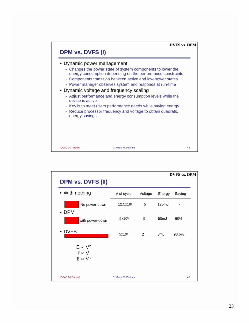
DPM vs. DVFS (I)DPM vs. DVFS (I)
• Dynamic power management- Changes the power state of system components to lower the
energy consumption depending on the performance constraints- Components transition between active and low-power states- Power manager observes system and responds at run-time
• Dynamic voltage and frequency scaling- Adjust performance and energy consumption levels while the
device is active- Key is to meet users performance needs while saving energy- Reduce processor frequency and voltage to obtain quadratic
energy savings
DVFS vs. DPM
46E. Macii, M. PedramICCAD’04 Tutorial
DPM vs. DVFS (II)DPM vs. DVFS (II)
• With nothing
• DPM
• DVFS
No power-down
with power-down
# of cycle Voltage Energy Saving
12.5x10⁶ 5 125mJ -
5x10⁶ 5 50mJ 60%
5x10⁶ 2 8mJ 93.6%
E µ V2
f µ VE µ V3
DVFS vs. DPM
24
47E. Macii, M. PedramICCAD’04 Tutorial
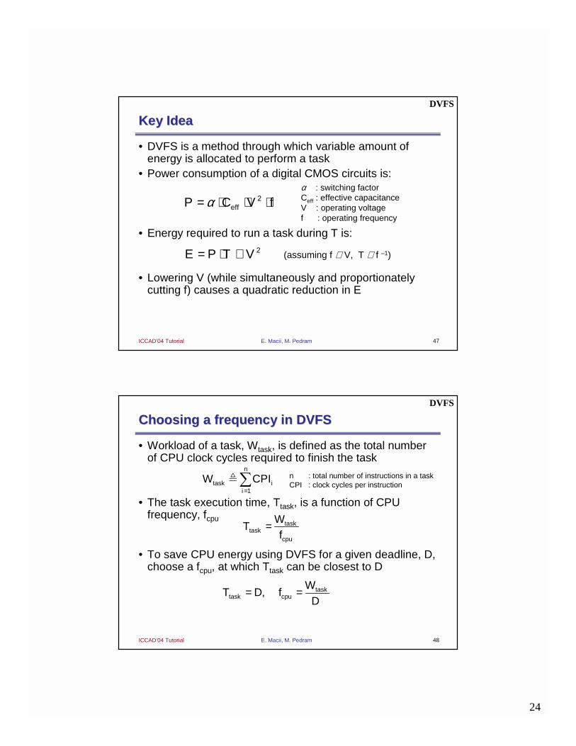
Key IdeaKey Idea
• DVFS is a method through which variable amount of energy is allocated to perform a task
• Power consumption of a digital CMOS circuits is:
• Energy required to run a task during T is:
• Lowering V (while simultaneously and proportionately cutting f) causes a quadratic reduction in E
α= ⋅ ⋅ ⋅2effP C V f
α : switching factorCeff : effective capacitanceV : operating voltagef : operating frequency
= ⋅ ∝ 2E P T V (assuming f ∝ V, T ∝ f –1)
DVFS
48E. Macii, M. PedramICCAD’04 Tutorial
Choosing a frequency in DVFSChoosing a frequency in DVFS
• Workload of a task, Wtask, is defined as the total number of CPU clock cycles required to finish the task
• The task execution time, Ttask, is a function of CPU frequency, fcpu
• To save CPU energy using DVFS for a given deadline, D, choose a fcpu, at which Ttask can be closest to D
=∑
1
n
task ii
W CPI! n : total number of instructions in a taskCPI : clock cycles per instruction
= tasktask
cpu
WT
f
= =, tasktask cpu
WT D f
D
DVFS
25
49E. Macii, M. PedramICCAD’04 Tutorial
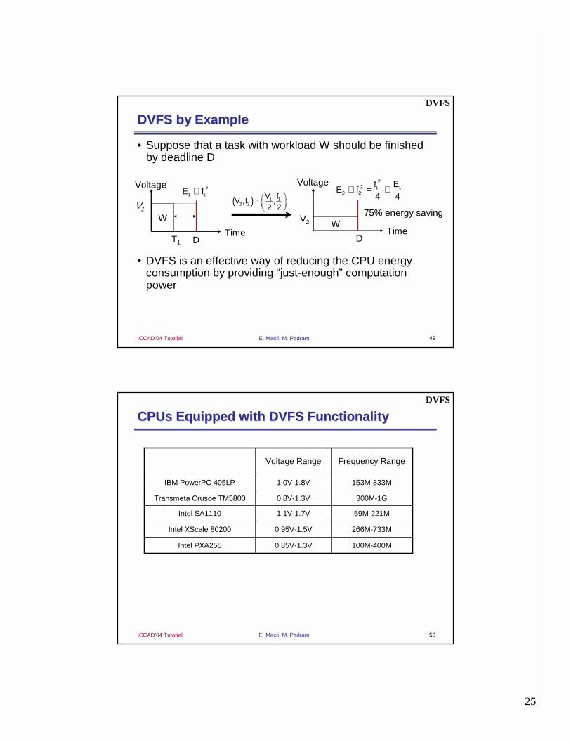
DVFS by ExampleDVFS by Example
• Suppose that a task with workload W should be finished by deadline D
• DVFS is an effective way of reducing the CPU energy consumption by providing “just-enough” computation power
WW
Time Time
V1
V2
Voltage Voltage
DT1
( ) =
, ,2 21 1
2 2
V fV f
∝ 21 1E f ∝ = ∝
22 1 1
2 2
f EE f
4 4
D
75% energy saving
DVFS
50E. Macii, M. PedramICCAD’04 Tutorial
266M-733M0.95V-1.5VIntel XScale 80200
59M-221M1.1V-1.7VIntel SA1110
100M-400M0.85V-1.3VIntel PXA255
300M-1G0.8V-1.3VTransmeta Crusoe TM5800
153M-333M1.0V-1.8VIBM PowerPC 405LP
Frequency RangeVoltage Range
CPUs Equipped with DVFS FunctionalityCPUs Equipped with DVFS FunctionalityDVFS
26
51E. Macii, M. PedramICCAD’04 Tutorial
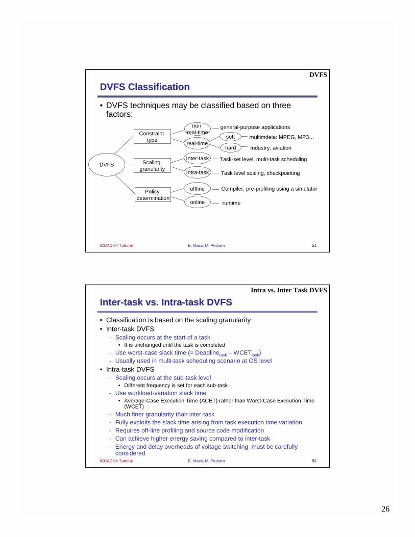
DVFS ClassificationDVFS Classification
• DVFS techniques may be classified based on three factors:
DVFS
Constraint type
Scaling granularity
Policy determination
real-time
non real-time
Inter-task
Intra-task
offline
online
general-purpose applications
soft
hard
multimdeia: MPEG, MP3…
Industry, aviation
Compiler, pre-profiling using a simulator
Task-set level, multi-task scheduling
Task level scaling, checkpointing
runtime
DVFS
52E. Macii, M. PedramICCAD’04 Tutorial
InterInter--task vs. Intratask vs. Intra--task DVFS task DVFS
• Classification is based on the scaling granularity• Inter-task DVFS
- Scaling occurs at the start of a task • It is unchanged until the task is completed
- Use worst-case slack time (= Deadlinetask – WCETtask)- Usually used in multi-task scheduling scenario at OS level
• Intra-task DVFS- Scaling occurs at the sub-task level
• Different frequency is set for each sub-task
- Use workload-variation slack time• Average-Case Execution Time (ACET) rather than Worst-Case Execution Time
(WCET)
- Much finer granularity than inter-task- Fully exploits the slack time arising from task execution time variation- Requires off-line profiling and source code modification - Can achieve higher energy saving compared to inter-task- Energy and delay overheads of voltage switching must be carefully
considered
Intra vs. Inter Task DVFS

27
53E. Macii, M. PedramICCAD’04 Tutorial
Performance vs. CPU Speed Performance vs. CPU Speed --11
• Dynamic voltage scaling on a low-power microprocessor,” Pouwelseet al., 2001
• Considered memory power/performance• Memory bandwidth is not linearly proportional to the CPU frequency
LART system- SA1100 processor-based- 32MB EDO-DRAM
60ns access time
faster at 133MHz than at 162MHz in case of memory bound applications
System Perf. vs. CPU Speed
Mem
ory
BW
in M
bps
CPU Clock Freq. In MHz
54E. Macii, M. PedramICCAD’04 Tutorial
Performance vs. CPU Speed Performance vs. CPU Speed --22
• Non-linearity of memory bandwidth also affects the power consumption
• Memory chip typically operates at 3.3V
System Perf. vs. CPU Speed
Memory power
CPU power
CPU Clock Freq. in MHz
Pow
er C
onsu
mpt
ion
in m
W
28
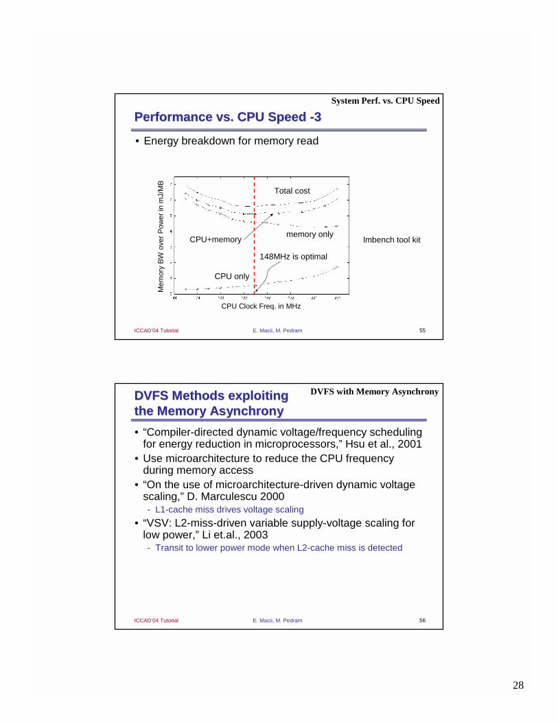
55E. Macii, M. PedramICCAD’04 Tutorial
Performance vs. CPU Speed Performance vs. CPU Speed --33
• Energy breakdown for memory read
lmbench tool kit
System Perf. vs. CPU Speed
CPU only
memory only
Total cost
CPU+memory
148MHz is optimal
CPU Clock Freq. in MHz
Mem
ory
BW
ove
r P
ower
in m
J/M
B
56E. Macii, M. PedramICCAD’04 Tutorial
DVFS Methods exploiting DVFS Methods exploiting the Memory Asynchronythe Memory Asynchrony
• “Compiler-directed dynamic voltage/frequency scheduling for energy reduction in microprocessors,” Hsu et al., 2001
• Use microarchitecture to reduce the CPU frequency during memory access
• “On the use of microarchitecture-driven dynamic voltage scaling,” D. Marculescu 2000- L1-cache miss drives voltage scaling
• “VSV: L2-miss-driven variable supply-voltage scaling for low power,” Li et.al., 2003- Transit to lower power mode when L2-cache miss is detected
DVFS with Memory Asynchrony
29
57E. Macii, M. PedramICCAD’04 Tutorial
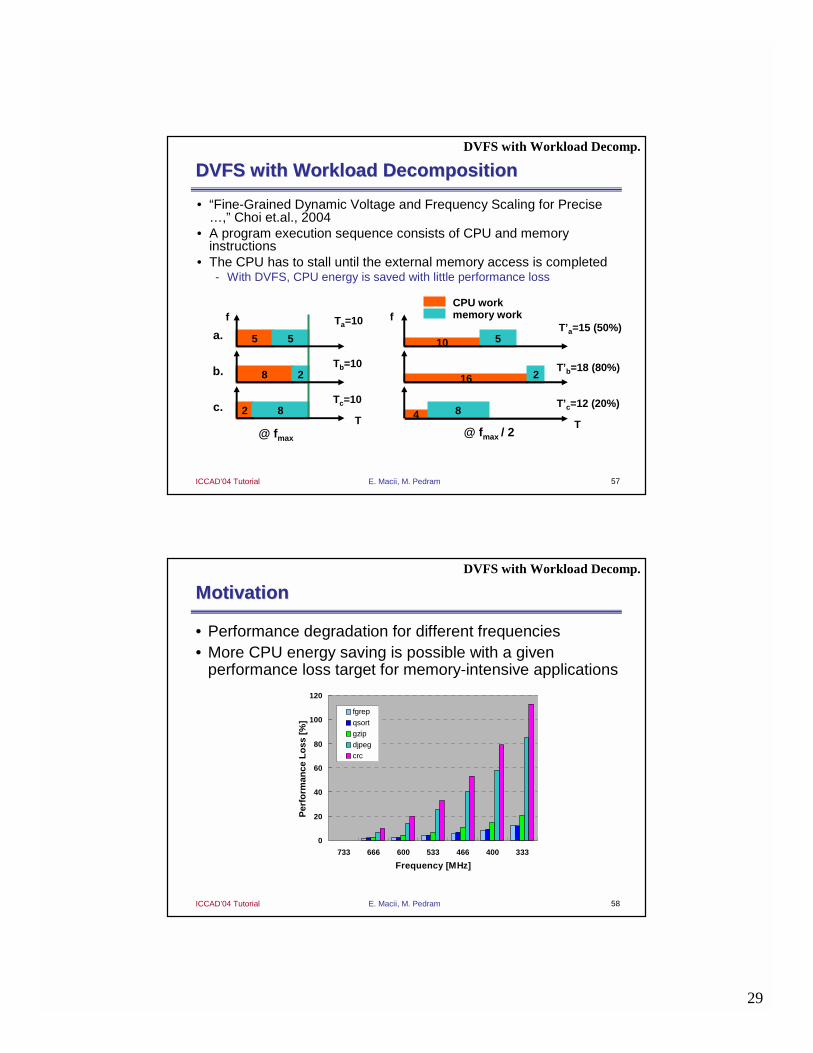
DVFS with Workload DecompositionDVFS with Workload Decomposition
• “Fine-Grained Dynamic Voltage and Frequency Scaling for Precise …,” Choi et.al., 2004
• A program execution sequence consists of CPU and memory instructions
• The CPU has to stall until the external memory access is completed- With DVFS, CPU energy is saved with little performance loss
5 5
2 8
8 2
T
f
@ fmax @ fmax / 2
10 5
4 8
16 2
f
T
a.
b.
c.
Ta=10
Tb=10
Tc=10
T’a=15 (50%)
T’b=18 (80%)
T’c=12 (20%)
CPU workmemory work
DVFS with Workload Decomp.
58E. Macii, M. PedramICCAD’04 Tutorial
MotivationMotivation
• Performance degradation for different frequencies• More CPU energy saving is possible with a given
performance loss target for memory-intensive applications
0
20
40
60
80
100
120
733 666 600 533 466 400 333
Frequency [MHz]
Per
form
ance
Lo
ss [
%]
fgrep
qsortgzipdjpegcrc
DVFS with Workload Decomp.
30
59E. Macii, M. PedramICCAD’04 Tutorial
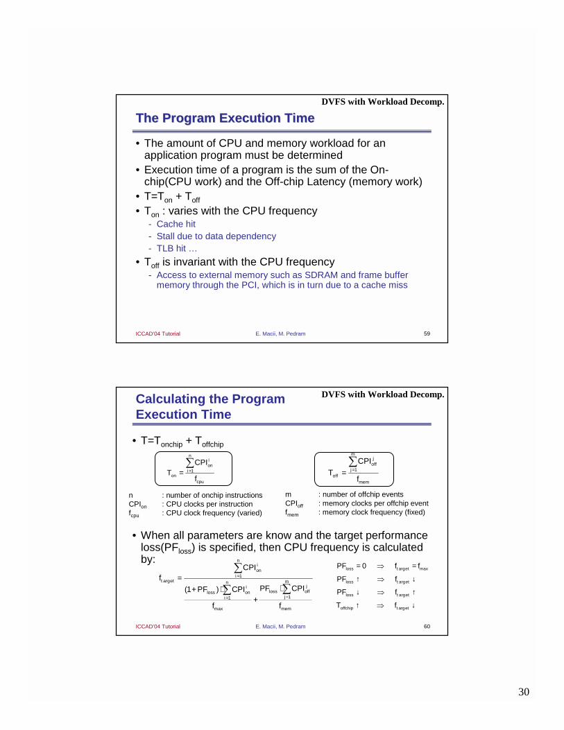
The Program Execution TimeThe Program Execution Time
• The amount of CPU and memory workload for an application program must be determined
• Execution time of a program is the sum of the On-chip(CPU work) and the Off-chip Latency (memory work)
• T=Ton + Toff
• Ton : varies with the CPU frequency- Cache hit- Stall due to data dependency- TLB hit …
• Toff is invariant with the CPU frequency- Access to external memory such as SDRAM and frame buffer
memory through the PCI, which is in turn due to a cache miss
DVFS with Workload Decomp.
60E. Macii, M. PedramICCAD’04 Tutorial
Calculating the Program Execution Time
• T=Tonchip + Toffchip
• When all parameters are know and the target performance loss(PFloss) is specified, then CPU frequency is calculated by:
==∑
1
nion
ion
cpu
CPIT
f==∑
1
mj
offj
offmem
CPIT
f
n : number of onchip instructionsCPIon : CPU clocks per instructionfcpu : CPU clock frequency (varied)
m : number of offchip eventsCPIoff : memory clocks per offchip eventfmem : memory clock frequency (fixed)
=
==
=⋅+ ⋅
+
∑
∑∑1
arg
11
max
(1 )
nion
it et mn
jiloss offloss on
ji
mem
CPIf
PF CPIPF CPI
f f
= ⇒ =
↑ ⇒ ↓
↓ ⇒ ↑
↑ ⇒ ↓
arg max
arg
arg
arg
0
loss t et
loss t et
loss t et
offchip t et
PF f f
PF f
PF f
T f
DVFS with Workload Decomp.
31
61E. Macii, M. PedramICCAD’04 Tutorial
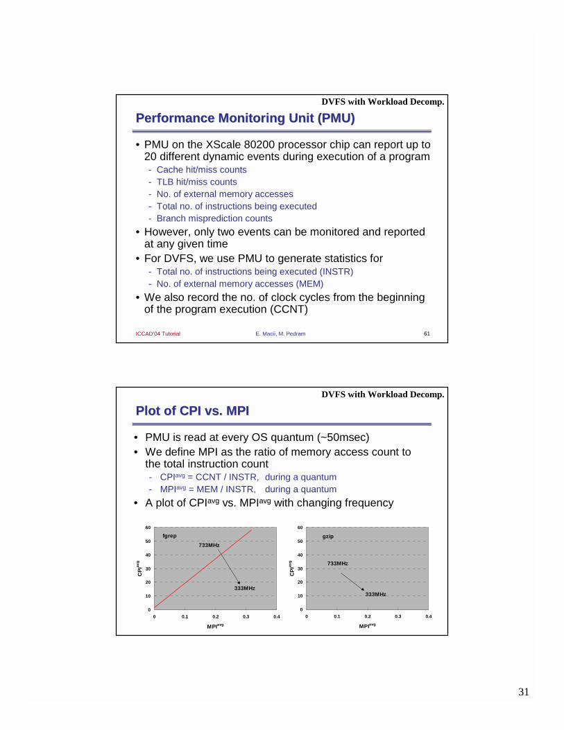
Performance Monitoring Unit (PMU)Performance Monitoring Unit (PMU)
• PMU on the XScale 80200 processor chip can report up to 20 different dynamic events during execution of a program- Cache hit/miss counts- TLB hit/miss counts- No. of external memory accesses- Total no. of instructions being executed- Branch misprediction counts
• However, only two events can be monitored and reported at any given time
• For DVFS, we use PMU to generate statistics for - Total no. of instructions being executed (INSTR)- No. of external memory accesses (MEM)
• We also record the no. of clock cycles from the beginning of the program execution (CCNT)
DVFS with Workload Decomp.
62E. Macii, M. PedramICCAD’04 Tutorial
Plot of CPI vs. MPIPlot of CPI vs. MPI
• PMU is read at every OS quantum (~50msec)• We define MPI as the ratio of memory access count to
the total instruction count - CPIavg = CCNT / INSTR, during a quantum- MPIavg = MEM / INSTR, during a quantum
• A plot of CPIavg vs. MPIavg with changing frequency
0
10
20
30
40
50
60
0 0.1 0.2 0.3 0.4
MPIavg
CP
Iavg
fgrep
733MHz
333MHz
0
10
20
30
40
50
60
0 0.1 0.2 0.3 0.4
MPIavg
CP
Iavg
gzip
333MHz
733MHz
DVFS with Workload Decomp.
32
63E. Macii, M. PedramICCAD’04 Tutorial
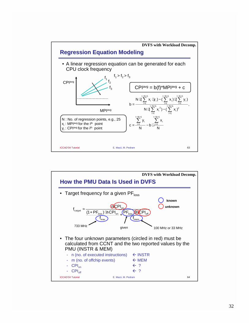
Regression Equation ModelingRegression Equation Modeling
• A linear regression equation can be generated for each CPU clock frequency
− + − + − +
= = =− + − +
= =
− + − +
= =
⋅ ⋅ − ⋅=
⋅ −
= − ⋅
∑ ∑ ∑
∑ ∑
∑ ∑
1 1 1
1 12 2
1
1 1
( ) ( ) ( ),
( ) ( )
t N t N t N
i i i ii t i t i t
t N t N
i ii t i
t N t N
i ii t i t
N x y x yb
N x x
y xc b
N N
MPIavg
CPIavg
CPIavg = b(f)*MPIavg + c
N : No. of regression points, e.g., 25xi : MPIavg for the ith pointyi : CPIavg for the ith point
f1f2f3
f1 > f2 > f3
DVFS with Workload Decomp.
64E. Macii, M. PedramICCAD’04 Tutorial
How the PMU Data Is Used in DVFSHow the PMU Data Is Used in DVFS
• Target frequency for a given PFloss
• The four unknown parameters (circled in red) must be calculated from CCNT and the two reported values by the PMU (INSTR & MEM)- n (no. of executed instructions) # INSTR- m (no. of offchip events) # MEM- CPIon # ?- CPIoff # ?
≈+ ⋅ ⋅+
arg
max
(1 )on
t etloss on loss off
mem
n CPIf
PF nCPI PF mCPIf f
known
unknown
100 MHz or 33 MHz733 MHz given
DVFS with Workload Decomp.
33
65E. Macii, M. PedramICCAD’04 Tutorial
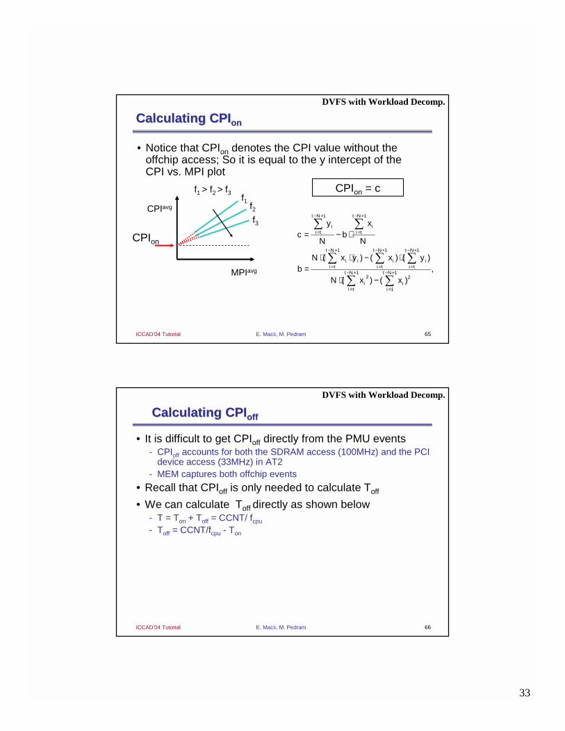
Calculating Calculating CPICPIonon
• Notice that CPIon denotes the CPI value without the offchip access; So it is equal to the y intercept of the CPI vs. MPI plot
− + − +
= =
− + − + − +
= = =− + − +
= =
= − ⋅
⋅ ⋅ − ⋅=
⋅ −
∑ ∑
∑ ∑ ∑
∑ ∑
1 1
1 1 1
1 12 2
1
( ) ( ) ( ),
( ) ( )
t N t N
i ii t i t
t N t N t N
i i i ii t i t i t
t N t N
i ii t i
y xc b
N N
N x y x yb
N x x
CPIon = c
MPIavg
CPIavg
CPIon
f1f2f3
f1 > f2 > f3
DVFS with Workload Decomp.
66E. Macii, M. PedramICCAD’04 Tutorial
Calculating Calculating CPICPIoffoff
• It is difficult to get CPIoff directly from the PMU events- CPIoff accounts for both the SDRAM access (100MHz) and the PCI
device access (33MHz) in AT2- MEM captures both offchip events
• Recall that CPIoff is only needed to calculate Toff
• We can calculate Toff directly as shown below- T = Ton + Toff = CCNT/ fcpu
- Toff = CCNT/fcpu - Ton
DVFS with Workload Decomp.
34
67E. Macii, M. PedramICCAD’04 Tutorial
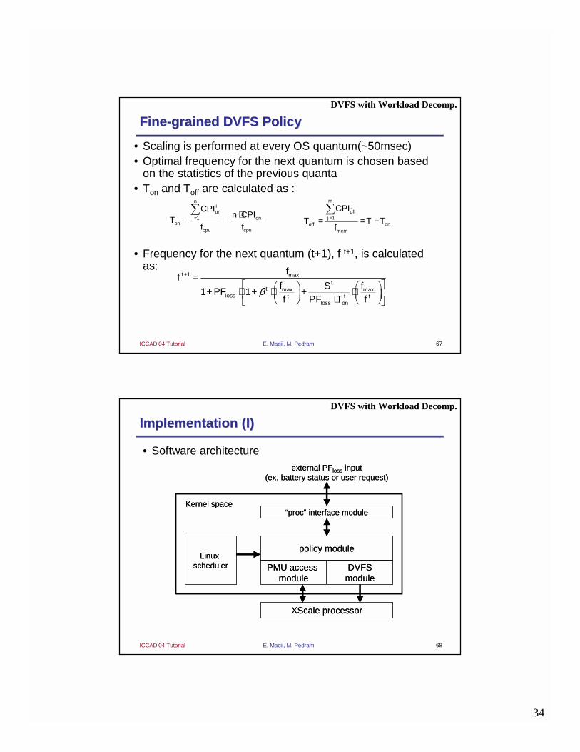
FineFine--grained DVFS Policygrained DVFS Policy
• Scaling is performed at every OS quantum(~50msec)• Optimal frequency for the next quantum is chosen based
on the statistics of the previous quanta• Ton and Toff are calculated as :
• Frequency for the next quantum (t+1), f t+1, is calculated as:
= ⋅= =∑
1
nion
onion
cpu cpu
CPIn CPI
Tf f
== = −∑
1
mj
offj
off onmem
CPIT T T
f
β
+ = + ⋅ + ⋅ + ⋅ ⋅
1 max
max max1 1
t
tt
loss t t tloss on
ff
f fSPF
f PF T f
DVFS with Workload Decomp.
68E. Macii, M. PedramICCAD’04 Tutorial
Implementation (I)Implementation (I)
• Software architecture
“proc” interface module
Linux scheduler
policy module
PMU access module
DVFSmodule
XScale processor
Kernel space
external PFloss input(ex, battery status or user request)
“proc” interface module
Linux scheduler
policy module
PMU access module
DVFSmodule
XScale processor
Kernel space
external PFloss input(ex, battery status or user request)
DVFS with Workload Decomp.
35
69E. Macii, M. PedramICCAD’04 Tutorial
DUT
ResistorPower split
DUT
ResistorPower split
DUT
V1
∆V = VDUT – V1I = ∆V / RP = I • V1
Sample40kHz
I
R
∆V
VDUT
Operating Voltage of DUT
DUT
V1
∆V = VDUT – V1I = ∆V / RP = I • V1
Sample40kHz
I
R
∆V
VDUT
Operating Voltage of DUT
Data Acquisition system
333
400
466
533
600
666
733
Frequency(MHz)
Voltage(V)
0.91
0.99
1.05
1.12
1.19
1.26
1.49
CPU Freq. vs. Volt. Relation
• A voltage in mapped to each CPU frequency• Voltage control circuitry is on-board• Power measurement with DAQ (DATA Acquisition)
Implementation (II)Implementation (II)DVFS with Workload Decomp.
70E. Macii, M. PedramICCAD’04 Tutorial
Experimental Results (I) Experimental Results (I)
• Power consumption vs. performance degradation
with DVFSwithout DVFS
0
500
1000
1500
2000
2500
0 0.2 0.4 0.6 0.8 1 1.2
Time [sec]
Po
wer
co
nsu
mp
tio
n [
mW
]
gzip, @733MHz
0.9684 sec avg. power : 789.5mW
0
500
1000
1500
0.4 0.41 0.42
0
500
1000
1500
2000
2500
0 0.2 0.4 0.6 0.8 1 1.2
Time [sec]
Po
wer
co
nsu
mp
tio
n [
mW
]
gzip, @733MHz
0.9684 sec avg. power : 789.5mW
0
500
1000
1500
0.4 0.41 0.42
0
500
1000
1500
2000
2500
0 0.2 0.4 0.6 0.8 1 1.2
Time [sec]
Po
wer
co
nsu
mp
tio
n [
mW
]
gzip, with 10% PFloss
1.0806 sec (11.6% PFloss)
avg. power : 338.7mW (52.1% energy saving)
0
500
1000
1500
0.4 0.41 0.42
0
500
1000
1500
2000
2500
0 0.2 0.4 0.6 0.8 1 1.2
Time [sec]
Po
wer
co
nsu
mp
tio
n [
mW
]
gzip, with 10% PFloss
1.0806 sec (11.6% PFloss)
avg. power : 338.7mW (52.1% energy saving)
0
500
1000
1500
0.4 0.41 0.42
DVFS with Workload Decomp.
36
71E. Macii, M. PedramICCAD’04 Tutorial
Experimental Results (II)Experimental Results (II)
• Measured PFloss with a variable performance loss target ranging from 5% to 20%
0
5
10
15
20
25
30
bf crc djpeg gzip math fgrep qsort
Act
ual
Per
form
ance
Lo
ss [
%]
5%
10%
15%
20%
Target Performace Loss
0
10
20
30
40
50
60
70
80
bf crc djpeg gzip math fgrep qsort
En
erg
y S
avin
g [
%]
5%
10%15%
20%
Target Performace Loss
DVFS with Workload Decomp.
72E. Macii, M. PedramICCAD’04 Tutorial
DVFS Considering the Total System EnergyDVFS Considering the Total System Energy
• “DVFS Considering Variable and Fixed Components of the System Power Dissipation,” Choi et al., 2004
• Most DVFS methods are concerned about the CPU energy reduction only- More precisely, dynamic portion of the CPU energy
• However, most systems comprise of many subsystems such as memory and peripheral devices- Battery lifetime also depends on power consumption in
subsystems, which is not affected by CPU frequency changes- Lowering CPU frequency can cause shorter battery lifetime due to
an increase in the standing and idle portions of the system energy consumption
DVFS for System Power Saving
37
73E. Macii, M. PedramICCAD’04 Tutorial
Total System Energy Variation in DVFSTotal System Energy Variation in DVFS
t 2t 3tTime
f1 f2 = f1/2 f3 = f1/3
E1=CV12f1t E2=E1/4 E3=E1/9
Pcpu
(a)
t 2t 3tTime
f1 f2 = f1/2 f3 = f1/3
E1=(Pcpu+Pperi) *t E2=(Pcpu/8 +Pperi)*2t E3=(Pcpu/27 +Pperi)*3tPcpu
Pperi
Pcpu+Pperi
(b)
For CPU, lower frequency gives lower energy consumption
For a system, lower frequency does not give lower energy consumption
DVFS for System Power Saving
74E. Macii, M. PedramICCAD’04 Tutorial
CPU Freq. for Minimum System EnergyCPU Freq. for Minimum System Energy
• Let γ denotes Pperipheral/Pcpu @fmax
• Based on the γ value, minimum system energy is obtained at different CPU freq.
γγγ
= ⋅ + ⋅
= ⋅ + ⋅ ⋅
= ⋅ + ⋅ ⋅
1
2
3
@ : (1 )
@ / 2 : (1/ 4 2 )
@ / 3 : (1/9 3 )
max cpu
max cpu
max cpu
f E P t
f E P t
f E P t
0
1
2
3
4
5
0 0.5 1 1.5 2
γγγγ
En
erg
y C
on
sum
pti
on
(ar
b)
E2
E1
E3IIIIII
Previous DVFS techniques only consider the case when γ is 0
Frequency setting to achieve minimum energy:
Region (I) : fmax /3Region (II) : fmax /2Region (III) : fmax
DVFS for System Power Saving
38
75E. Macii, M. PedramICCAD’04 Tutorial
System Power BreakdownSystem Power BreakdownDVFS for System Power Saving
• A system consists of the CPU and other sub-modules such as memory
• System power consumption can be broken into fixed vs. variable or standing vs. active components
fixed variable
idle
activestanding
Remains unchanged during the
task execution
idle + fixed
consumed when the systemis executing no useful task
consumed when the systemis executing some useful task
76E. Macii, M. PedramICCAD’04 Tutorial
Total System Power DissipationTotal System Power Dissipation
• Time-varying system power consumption
= =
+
= + + = +
= + + +
= ⋅
∑ ∑
∫
, , , , ,
, , , ,1 1
, ,
( ) ( ) ( )
( ) ( )
( )
n n n n n
n n
1
n n1
fix id le act s td actsys F sys sys F sys F sys F sys F
N Nstd act std act
cpu F cpu F m od i m od ii i
t T
sys F sys Ft
P t P P P t P P t
P P t P P t
E P t dt
power
timet1 t1+T
T
, ( )nsys FP t
, n
stdcpu FP
,std
mod iP
, ( )n
actcpu FP t
,act
mod iP
standing component in the CPU power at CPU frequency Fn
standing component in the ith
module power
active component in the CPU power at CPU frequency Fn
active component in the ith
module power
nFThe nth frequency setting, Fn(fn
cpu, fnint, fn
ext)
DVFS for System Power Saving
39
77E. Macii, M. PedramICCAD’04 Tutorial
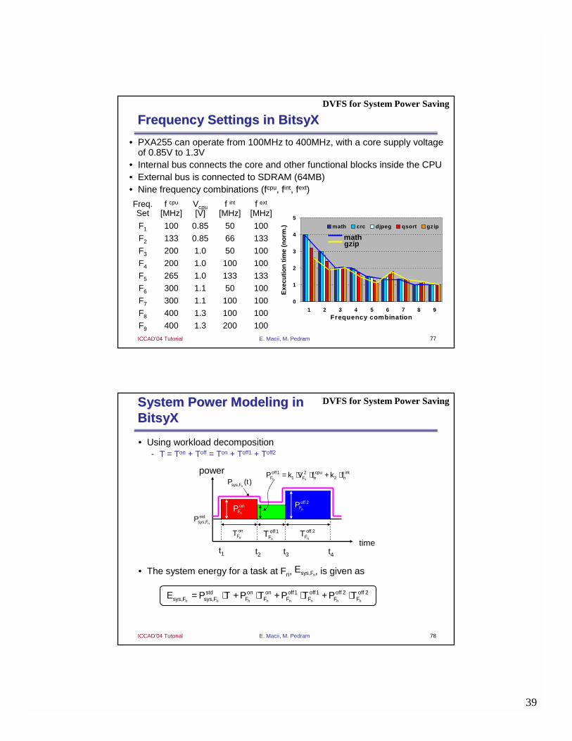
Frequency Settings in Frequency Settings in BitsyXBitsyX
1331331.0265F5
1001001.0200F4
100501.0200F3
133660.85133F2
1.3
1.3
1.1
1.1
0.85
Vcpu[V]
100200400F9
10050100F1
10050300F6
100100300F7
100100400F8
Freq. Set
f int
[MHz]f ext
[MHz]f cpu
[MHz]
0
1
2
3
4
5
1 2 3 4 5 6 7 8 9Frequency combination
Exe
cuti
on
tim
e (n
orm
.)
math crc djpeg qsort gzip
mathgzip
• PXA255 can operate from 100MHz to 400MHz, with a core supply voltage of 0.85V to 1.3V
• Internal bus connects the core and other functional blocks inside the CPU• External bus is connected to SDRAM (64MB)• Nine frequency combinations (fcpu, fint, fext)
DVFS for System Power Saving
78E. Macii, M. PedramICCAD’04 Tutorial
System Power Modeling in System Power Modeling in BitsyXBitsyX
• Using workload decomposition- T = Ton + Toff = Ton + Toff1 + Toff2
• The system energy for a task at Fn, , is given as
= ⋅ + ⋅ + ⋅ + ⋅, ,n n n n n n n n
std on on off1 off1 off 2 off 2sys F sys F F F F F F FE P T P T P T P T
power
timet1 t4t2
n
off 2FP
, n
stdsys FP
n
onFT
n
off 2FT
n
onFP
, ( )nsys FP t
n
off1FT
t3
= ⋅ ⋅ + ⋅n n
off1 2 cpu intF 1 F n 2 nP k V f k f
, nsys FE
DVFS for System Power Saving
40
79E. Macii, M. PedramICCAD’04 Tutorial
Accuracy of the System Energy ModelAccuracy of the System Energy Model
• The estimated energy consumption for “djpeg”- The average error rate is less than 4%
Extracted parameters= ⋅ + ⋅ + ⋅ + ⋅, ,n n n n n n n n
std on on off1 off1 off 2 off 2sys F sys F F F F F F FE P T P T P T P T
DVFS for System Power Saving
785*1.3310183361836F5
7857662171728F4
7854562181699F3
785*1.334791481757F2
1733
1113
885
575
363
675
673
378
344
89
7851963F9
7851665F1
7851732F6
7851778F7
7851869F8
Freq. set
k1 = 0.73 [nF], k2 = 6.2 [V2nF]
⋅ ⋅ + ⋅~n n
off 2 cpu intint,F 1 F n 2 nP k V f k f
,
( )n
stdsys FP
m W
( )n
onFP
m W,
( )
n
offext FP
m W
( )n
offin t,FP
m W
0
10
20
30
40
1 2 3 4 5 6 7 8 9
Frequency combination
En
erg
y co
nsu
mp
tio
n [
J]
measured
estimated
80E. Macii, M. PedramICCAD’04 Tutorial
Determining the Optimal Determining the Optimal Frequency SettingFrequency Setting
DVFS for System Power Saving
• Consider both timing and minimal system energy constraint- For a timing constraint, we use the performance loss factor (PFloss)
which is defined as:
• Pseudo code for optimal frequency selection
1. Ψ = { Fmin , …, Fmax }, Γ = {φ }, and Emin = ∞
2. for every frequency setting Fn in Ψ
3. if ( )
4. Γ = Γ ∪ Fn ;
5. for every frequency setting Fn in Γ
6. calculate system energy using proposed model
7. if ( ≤ Emin )
8. Emin = ; Fopti+1 = Fn ;
≤ + ⋅(1 )maxn
iloss FF
T PF Ti+1
, nsys FE
Timing constraint
Energy optimization
( )−= n max
max
F F
lossF
T TPF
T: task execution time at Fn: task execution time at Fmax
nFT
maxFT
, nsys FE , nsys FE
41
81E. Macii, M. PedramICCAD’04 Tutorial
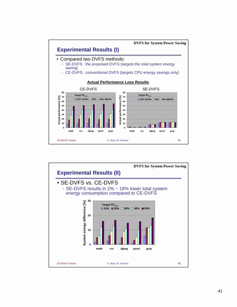
Experimental Results (I)Experimental Results (I)DVFS for System Power Saving
• Compared two DVFS methods:- SE-DVFS : the proposed DVFS (targets the total system energy
saving)- CE-DVFS : conventional DVFS (targets CPU energy savings only)
0
10
20
30
40
50
60
70
80
math crc djpeg qsort gzip
Act
ual
per
form
ance
[%
]
10% 20% 30% 40% 50%
Target PFloss
0
10
20
30
40
50
60
70
80
math crc djpeg qsort gzip
Act
ual
per
form
ance
[%
]
10% 20% 30% 40% 50%
Target PFloss
0
10
20
30
40
50
60
70
80
math crc djpeg qsort gzip
Act
ual
per
form
ance
[%
]
10% 20% 30% 40% 50%
Target PFloss
0
10
20
30
40
50
60
70
80
math crc djpeg qsort gzip
Act
ual
per
form
ance
[%
]
10% 20% 30% 40% 50%
Target PFloss
Actual Performance Loss Results
SE-DVFSCE-DVFS
82E. Macii, M. PedramICCAD’04 Tutorial
Experimental Results (II)Experimental Results (II)
0
10
20
30
math crc djpeg qsort gzip
Sys
tem
en
erg
y d
iffe
ren
ce [
%]
10% 20% 30% 40% 50%Target PFloss
0
10
20
30
math crc djpeg qsort gzip
Sys
tem
en
erg
y d
iffe
ren
ce [
%]
10% 20% 30% 40% 50%Target PFloss
DVFS for System Power Saving
• SE-DVFS vs. CE-DVFS- SE-DVFS results in 2% ~ 18% lower total system
energy consumption compared to CE-DVFS
42
83E. Macii, M. PedramICCAD’04 Tutorial
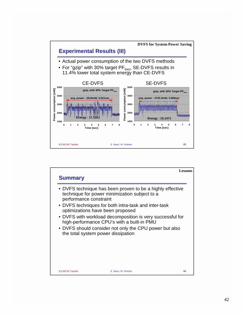
Experimental Results (III)Experimental Results (III)
• Actual power consumption of the two DVFS methods• For “gzip” with 30% target PFloss, SE-DVFS results in
11.4% lower total system energy than CE-DVFS
1000
2000
3000
4000
5000
0 1 2 3 4 5 6 7 8Time [sec]
Po
wer
co
nsu
mp
tio
n [
mW
]
gzip, with 30% Target PFloss
avg. power : 2619mW, 6.531sec
Energy : 17.105J1000
2000
3000
4000
5000
0 1 2 3 4 5 6 7 8Time [sec]
Po
wer
co
nsu
mp
tio
n [
mW
]
gzip, with 30% Target PFloss
avg. power : 2619mW, 6.531sec
Energy : 17.105J1000
2000
3000
4000
5000
0 1 2 3 4 5 6 7 8Time [sec]
Po
wer
co
nsu
mp
tio
n [
mW
]
gzip, with 30% Target PFloss
avg. power : 2720.3mW, 5.568sec
Energy : 15.147J1000
2000
3000
4000
5000
0 1 2 3 4 5 6 7 8Time [sec]
Po
wer
co
nsu
mp
tio
n [
mW
]
gzip, with 30% Target PFloss
avg. power : 2720.3mW, 5.568sec
Energy : 15.147J
SE-DVFSCE-DVFS
DVFS for System Power Saving
84E. Macii, M. PedramICCAD’04 Tutorial
SummarySummary
• DVFS technique has been proven to be a highly effective technique for power minimization subject to a performance constraint
• DVFS techniques for both intra-task and inter-task optimizations have been proposed
• DVFS with workload decomposition is very successful for high-performance CPU’s with a built-in PMU
• DVFS should consider not only the CPU power but also the total system power dissipation
Lessons

43
85E. Macii, M. PedramICCAD’04 Tutorial
Challenges and Directions in Challenges and Directions in Low Power DesignLow Power Design• Subthreshold leakage control in standby as well as sleep
modes without adversely effecting the circuit performance and cost
• Statistical parameter variation and its impact on leakage current modeling and calculation
• Physical design tools that support multiple voltage islands, body bias control, and power gating
• Full-chip DVFS considering the total system energy consumption
• Combining DVFS and DPM at system level • Combining Dual-Vth and MTCOMS (power gating) at RT-
level and below
Putting It All Together
86E. Macii, M. PedramICCAD’04 Tutorial
Challenges and Directions in Challenges and Directions in Low Power DesignLow Power Design• Need to address all major consumers of power in
microelectronic systems, including the on-chip drivers, memory, I/O drivers, TFT LCD, radio transceiver, etc.
• Power-aware bus encoding techniques (for off-chip buses as well as on-chip buses in SoC designs) which account for various noise sources e.g., the capacitive and inductive crosstalk, and power plane variations
• Taking the battery characteristics (rate-capacity curve, energy recovery effect, and battery aging) into consideration when developing energy-aware design solutions
• Power delivery issues
Putting It All Together


![8 TCCS4 Task F Georgescu-Modelling and Simulation of CO2 Leakage Mechanisms Version2[1]](https://static.fdocuments.net/doc/165x107/577cc9fa1a28aba711a519f3/8-tccs4-task-f-georgescu-modelling-and-simulation-of-co2-leakage-mechanisms.jpg)