LDC1101 1.8-V High-Resolution, High-Speed … simultaneous with a high-resolution L measurement...
59
GND MCU VDD SPI Peripheral 1.8V 1.8V SCLK CSB MISO MOSI CLKOUT Sensor RP + L Meas INA INB LDC1101 VDD Registers + Logic GND SPI CLKIN SCLK CSB SDO SDI High Res L Meas Sensor Driver CLDO Threshold Compare Product Folder Sample & Buy Technical Documents Tools & Software Support & Community Reference Design An IMPORTANT NOTICE at the end of this data sheet addresses availability, warranty, changes, use in safety-critical applications, intellectual property matters and other important disclaimers. PRODUCTION DATA. LDC1101 SNOSD01D – MAY 2015 – REVISED OCTOBER 2016 LDC1101 1.8-V High-Resolution, High-Speed Inductance-to-Digital Converter 1 1 Features 1• Wide Operating Voltage Range: 1.8 V to 3.3 V • Sensor Frequency Range: 500 kHz to 10 MHz • R P Resolution: 16-Bit • L Resolution: 16- or 24-Bit • 180-kSPS Conversion Rate • Threshold Detection Functionality • 1% Part-to-Part Variation in R P Measurement • Supply Current: – 1.4-μA Shutdown mode – 135-μA Sleep mode – 1.9-mA Active Mode (no sensor connected) • Sub-Micron Distance Resolution Achievable • Remote Sensor Placement Isolating the LDC from Harsh Environments • Robust Against Environmental Interferences such as Oil, Water, Dirt, or Dust • Minimal External Components • Magnet-Free Operation • Operating Temperature: –40°C to +125°C 2 Applications • High-Speed Gear Counting • High-Speed Event Counting • Motor Speed Sensing • Knobs and Dials for Appliances, Automotive, and Consumer Applications • HMI for Appliances, Automotive, and Consumer Applications • Buttons and Keypads • Motor Control • Metal Detection 3 Description The LDC1101 is a 1.8-V to 3.3-V, high-resolution inductance-to-digital converter for short-range, high- speed, contactless sensing of position, rotation, or motion, enabling reliable, accurate measurements even in the presence of dust or dirt, making it ideal for open or harsh environments. The LDC1101 features dual inductive measurement cores, allowing for > 150 ksps 16-bit R P and L measurements simultaneous with a high-resolution L measurement which can sample at > 180 ksps with a resolution of up to 24 bits. The LDC1101 includes a threshold-compare function which can be dynamically updated while the device is running. Inductive sensing technology enables precise measurement of linear/angular position, displacement, motion, compression, vibration, metal composition, and many other applications in markets including automotive, consumer, computer, industrial, medical, and communications. Inductive sensing offers better performance and reliability at lower cost than other, competing solutions. The LDC1101 offers these benefits of inductive sensing in a small 3-mm × 3-mm 10-pin VSON package. The LDC1101 can be easily configured by a microcontroller using the 4-pin SPI™. Device Information (1) PART NUMBER PACKAGE BODY SIZE (NOM) LDC1101 VSON (10) 3.00 mm × 3.00 mm (1) For all available packages, see the orderable addendum at the end of the data sheet. 4 Simplified Schematic
Transcript of LDC1101 1.8-V High-Resolution, High-Speed … simultaneous with a high-resolution L measurement...
GND
MCU
VDD
SPIPeripheral
1.8V1.8V
SCLK
CSB
MISOMOSI
CLKOUT
Sensor
RP + L Meas
INA
INB
LDC1101VDD
Registers + Logic
GND
SPI
CLKIN
SCLK
CSB
SDO
SDI
High Res L Meas
Sensor Driver
CLDO
ThresholdCompare
Product
Folder
Sample &Buy
Technical
Documents
Tools &
Software
Support &Community
ReferenceDesign
An IMPORTANT NOTICE at the end of this data sheet addresses availability, warranty, changes, use in safety-critical applications,intellectual property matters and other important disclaimers. PRODUCTION DATA.
LDC1101SNOSD01D –MAY 2015–REVISED OCTOBER 2016
LDC1101 1.8-V High-Resolution, High-Speed Inductance-to-Digital Converter
1
1 Features1• Wide Operating Voltage Range: 1.8 V to 3.3 V• Sensor Frequency Range: 500 kHz to 10 MHz• RP Resolution: 16-Bit• L Resolution: 16- or 24-Bit• 180-kSPS Conversion Rate• Threshold Detection Functionality• 1% Part-to-Part Variation in RP Measurement• Supply Current:
– 1.4-µA Shutdown mode– 135-µA Sleep mode– 1.9-mA Active Mode (no sensor connected)
• Sub-Micron Distance Resolution Achievable• Remote Sensor Placement Isolating the LDC from
Harsh Environments• Robust Against Environmental Interferences such
as Oil, Water, Dirt, or Dust• Minimal External Components• Magnet-Free Operation• Operating Temperature: –40°C to +125°C
2 Applications• High-Speed Gear Counting• High-Speed Event Counting• Motor Speed Sensing• Knobs and Dials for Appliances, Automotive, and
Consumer Applications• HMI for Appliances, Automotive, and Consumer
Applications• Buttons and Keypads• Motor Control• Metal Detection
3 DescriptionThe LDC1101 is a 1.8-V to 3.3-V, high-resolutioninductance-to-digital converter for short-range, high-speed, contactless sensing of position, rotation, ormotion, enabling reliable, accurate measurementseven in the presence of dust or dirt, making it idealfor open or harsh environments.
The LDC1101 features dual inductive measurementcores, allowing for > 150 ksps 16-bit RP and Lmeasurements simultaneous with a high-resolution Lmeasurement which can sample at > 180 ksps with aresolution of up to 24 bits. The LDC1101 includes athreshold-compare function which can be dynamicallyupdated while the device is running.
Inductive sensing technology enables precisemeasurement of linear/angular position,displacement, motion, compression, vibration, metalcomposition, and many other applications in marketsincluding automotive, consumer, computer, industrial,medical, and communications. Inductive sensingoffers better performance and reliability at lower costthan other, competing solutions.
The LDC1101 offers these benefits of inductivesensing in a small 3-mm × 3-mm 10-pin VSONpackage. The LDC1101 can be easily configured by amicrocontroller using the 4-pin SPI™.
Device Information(1)
PART NUMBER PACKAGE BODY SIZE (NOM)LDC1101 VSON (10) 3.00 mm × 3.00 mm
(1) For all available packages, see the orderable addendum atthe end of the data sheet.
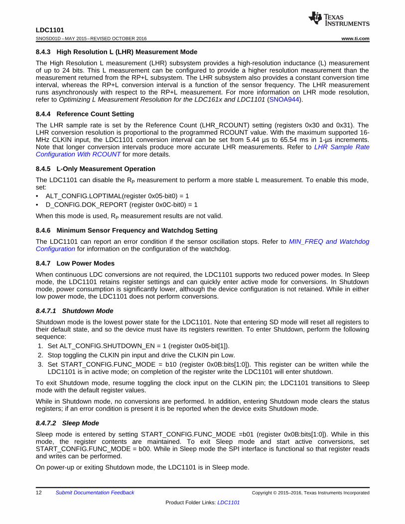
4 Simplified Schematic
2
LDC1101SNOSD01D –MAY 2015–REVISED OCTOBER 2016 www.ti.com
Product Folder Links: LDC1101
Submit Documentation Feedback Copyright © 2015–2016, Texas Instruments Incorporated
Table of Contents1 Features .................................................................. 12 Applications ........................................................... 13 Description ............................................................. 14 Simplified Schematic............................................. 15 Revision History..................................................... 26 Pin Configuration and Functions ......................... 47 Specifications......................................................... 5
7.1 Absolute Maximum Ratings ...................................... 57.2 ESD Ratings ............................................................ 57.3 Recommended Operating Conditions....................... 57.4 Thermal Information .................................................. 57.5 Electrical Characteristics........................................... 67.6 Digital Interface ......................................................... 67.7 Timing Requirements ................................................ 77.8 Typical Characteristics .............................................. 8
8 Detailed Description ............................................ 108.1 Overview ................................................................. 108.2 Functional Block Diagram ....................................... 108.3 Feature Description................................................. 10
8.4 Device Functional Modes........................................ 118.5 Programming.......................................................... 138.6 Register Maps ........................................................ 15
9 Application and Implementation ........................ 319.1 Application Information............................................ 319.2 Typical Application ................................................. 42
10 Power Supply Recommendations ..................... 4711 Layout................................................................... 47
11.1 Layout Guidelines ................................................. 4711.2 Layout Example .................................................... 48
12 Device and Documentation Support ................. 4912.1 Device Support .................................................... 4912.2 Documentation Support ........................................ 4912.3 Community Resources.......................................... 4912.4 Trademarks ........................................................... 4912.5 Electrostatic Discharge Caution............................ 4912.6 Glossary ................................................................ 50
13 Mechanical, Packaging, and OrderableInformation ........................................................... 50
5 Revision History
Changes from Revision C (February 2016) to Revision D Page
• Added link to Application Note SNOA944 ............................................................................................................................ 12• Changed RPMAX_DIS field name to HIGH_Q_SENSOR, as this is clearer for when to use this mode. .......................... 16• Changed location of notes detailing register read sequence from inside field entry in table to paragraph under
register title. .......................................................................................................................................................................... 25• Changed Field R/W value to R/W. ...................................................................................................................................... 26• Added links to LDC1101 Reference Designs ...................................................................................................................... 31• Added clarification on L-only mode or RP+L mode in example configuration .................................................................... 44• Changed incorrect value in table ......................................................................................................................................... 44
Changes from Revision B (July 2015) to Revision C Page
• Added top navigator icon for TI Designs ............................................................................................................................... 1• Changed "8.6 µs" to "5.44 µs" .............................................................................................................................................. 12• Changed "87.38 ms" to "65.54 ms" ...................................................................................................................................... 12• Changed "Valid range: 2 ≤ RCOUNT[15:8]..." to "Valid range: 2 ≤ RCOUNT[15:0]..." ........................................................ 26• Added "When LHR_OFFSET =0x0000, ƒSENSOR can be determined by:"............................................................................ 28
Changes from Revision A (June 2015) to Revision B Page
• Changed Register type and reset values for some fields which where incomplete. ............................................................ 16• Changed NAME to INTB_MODE.......................................................................................................................................... 21• Changed DRDY to INTB in INTB2SDO field descriiption..................................................................................................... 21• Changed RP Threshold and L Threshold field names in RP_HI_LON and L_HI_LON fields ............................................. 24• Changed Incorrect resistance value ..................................................................................................................................... 43• Changed Calculations of reference count setting................................................................................................................. 44
3
LDC1101www.ti.com SNOSD01D –MAY 2015–REVISED OCTOBER 2016
Product Folder Links: LDC1101
Submit Documentation FeedbackCopyright © 2015–2016, Texas Instruments Incorporated
Changes from Original (May 2015) to Revision A Page
• Added full datasheet to replace the Product Preview ............................................................................................................ 1
1
3
SDO/INTB
4
CLKIN
SCLK
5 INB6
INA7
GND8
VDD9
SDI
CLDO10
2
CSB
DAP
4
LDC1101SNOSD01D –MAY 2015–REVISED OCTOBER 2016 www.ti.com
Product Folder Links: LDC1101
Submit Documentation Feedback Copyright © 2015–2016, Texas Instruments Incorporated
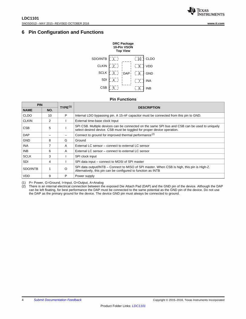
(1) P= Power, G=Ground, I=Input, O=Output, A=Analog(2) There is an internal electrical connection between the exposed Die Attach Pad (DAP) and the GND pin of the device. Although the DAP
can be left floating, for best performance the DAP must be connected to the same potential as the GND pin of the device. Do not usethe DAP as the primary ground for the device. The device GND pin must always be connected to ground.
6 Pin Configuration and Functions
DRC Package10-Pin VSON
Top View
Pin FunctionsPIN
TYPE (1) DESCRIPTIONNAME NO.CLDO 10 P Internal LDO bypassing pin. A 15-nF capacitor must be connected from this pin to GND.CLKIN 2 I External time-base clock Input
CSB 5 I SPI CSB. Multiple devices can be connected on the same SPI bus and CSB can be used to uniquelyselect desired device. CSB must be toggled for proper device operation.
DAP – – Connect to ground for improved thermal performance (2)
GND 8 G GroundINA 7 A External LC sensor – connect to external LC sensorINB 6 A External LC sensor – connect to external LC sensorSCLK 3 I SPI clock inputSDI 4 I SPI data input – connect to MOSI of SPI master
SDO/INTB 1 O SPI data output/INTB – Connect to MISO of SPI master. When CSB is high, this pin is High-Z.Alternatively, this pin can be configured to function as INTB
VDD 9 P Power supply
5
LDC1101www.ti.com SNOSD01D –MAY 2015–REVISED OCTOBER 2016
Product Folder Links: LDC1101
Submit Documentation FeedbackCopyright © 2015–2016, Texas Instruments Incorporated
(1) Stresses beyond those listed under Absolute Maximum Ratings may cause permanent damage to the device. These are stress ratingsonly, which do not imply functional operation of the device at these or any other conditions beyond those indicated under RecommendedOperating Conditions. Exposure to absolute-maximum-rated conditions for extended periods may affect device reliability.
(2) Maximum voltage across any two pins is VDD+0.3.
7 Specifications
7.1 Absolute Maximum Ratingsover operating free-air temperature range (unless otherwise noted) (1)
MIN MAX UNITVDD Supply voltage range 3.6 V
ViVoltage on INA, INB –0.3 2.3 VVoltage on CLDO –0.3 1.9 VVoltage on any other pin (2) –0.3 VDD + 0.3 V
TJ Junction temperature –55 125 °CTstg Storage temperature –65 125 °C
(1) JEDEC document JEP155 states that 500-V HBM allows safe manufacturing with a standard ESD control process.(2) JEDEC document JEP157 states that 250-V CDM allows safe manufacturing with a standard ESD control process.
7.2 ESD RatingsVALUE UNIT
V(ESD)Electrostaticdischarge
Human-body model (HBM), per ANSI/ESDA/JEDEC JS-001 (1) ±2000V
Charged-device model (CDM), per JEDEC specification JESD22-C101 (2) ±1000
7.3 Recommended Operating Conditionsover operating free-air temperature range (unless otherwise noted)
MIN NOM MAX UNITVDD Supply voltage 1.71 3.46 VTJ Junction temperature –40 125 °C
(1) For more information about traditional and new thermal metrics, see the Semiconductor and IC Package Thermal Metrics applicationreport, SPRA953.
7.4 Thermal Information
THERMAL METRIC (1)LDC1101
UNITDRC (VSON)10 PINS
RθJA Junction-to-ambient thermal resistance 44.2 °C/WRθJC(top) Junction-to-case (top) thermal resistance 50.1 °C/WRθJB Junction-to-board thermal resistance 19.6 °C/WψJT Junction-to-top characterization parameter 0.7 °C/WψJB Junction-to-board characterization parameter 19.8 °C/WRθJC(bot) Junction-to-case (bottom) thermal resistance 4.4 °C/W
6
LDC1101SNOSD01D –MAY 2015–REVISED OCTOBER 2016 www.ti.com
Product Folder Links: LDC1101
Submit Documentation Feedback Copyright © 2015–2016, Texas Instruments Incorporated
(1) Register values are represented as either binary (b is the prefix to the digits), or hexadecimal (0x is the prefix to the digits). Decimalvalues have no prefix.
(2) Limits are ensured by testing, design, or statistical analysis at 25°C. Limits over the operating temperature range are ensured throughcorrelation using statistical quality control (SQC) method.
(3) Typical values represent the most likely parametric norm as determined at the time of characterization. Actual typical values may varyover time and will also depend on the application and configuration. The typical values are not tested and are not verified on shippedproduction material.
7.5 Electrical CharacteristicsOver recommended operating conditions unless otherwise noted. VDD = 1.8 V, TA = 25°C.
PARAMETER TEST CONDITION (1) MIN (2) TYP (3) MAX (2) UNIT
POWER
VDD Supply voltage 1.71 3.46 V
IDD Supply current START_CONFIG= 0x00, no sensor connected 1.9 2.7 mA
IDDSSupply current including sensorcurrent
ƒCLKIN = 16 MHz, ƒSENSOR = 2 MHz,START_CONFIG = 0x00 3.2 mA
IDDSL Sleep mode supply current START_CONFIG =0x01 135 180 µA
ISD Shutdown mode supply current 1.4 6.7 µA
SENSOR
RP Measurement part-to-partvariation
RESP_TIME= 6144, D_CONFIG=0x00,ALT_CONFIG=0x00, START_CONFIG = 0x00,ƒSENSOR = 2 MHz
1%
ISENSORMAX Sensor maximum current drive RP_MIN = b111, START_CONFIG=0x00,D_CONFIG=0x00, ALT_CONFIG=0x00 0.598 0.6 0.602 mA
ISENSORMIN Sensor minimum current driveRP_MAX = b000, HIGH_Q_SENSOR=b0,START_CONFIG=0x00, D_CONFIG=0x00,ALT_CONFIG=0x00
4.7 µA
ƒSENSOR Sensor resonant frequency Device settings and Sensor compliant as detailed inLDC1101 RP Configuration 0.5 10 MHz
RPRES RP Measurement resolution 16 bits
LRES
Inductance sensing resolution –RP+L Mode 16 bits
Inductance sensing resolution –LHR Mode 24 bits
AOSC Sensor oscillation amplitude INA – INB, START_CONFIG=0x00,D_CONFIG=0x00, ALT_CONFIG=0x00 1.2 VPP
DETECTION
tS_MINMinimum response time (RP+Lmode) RP+L Mode, RESP_TIME=b010 192
÷ ƒSENSORs
tS_MAXMaximum response time (RP+Lmode) RP+L Mode, RESP_TIME=b111 6144
÷ ƒSENSORs
Ts_MAXHigh Res L maximum measurementinterval
LHR_REF_COUNT=0xFFFF,START_CONFIG=0x00
(220+39)÷ ƒCLKIN
s
SRMAXRP RP+L Mode maximum sample rate ƒCLKIN=16 MHz, ƒSENSOR = 10 MHz,RESP_TIME=b010 156.25 kSPS
SRMAXLHigh Res L Mode maximum samplerate
High Resolution L Mode,LHR_REF_COUNT=0x0002, ƒCLKIN=16 MHz 183.8 kSPS
FREQUENCY REFERENCE
fCLKIN Reference input frequency 1 16 MHz
DCfin Reference duty cycle 40% 60%
VIH Input high voltage (Logic “1”) 0.8 × VDD V
VIL Input low voltage (Logic “0”) 0.2 × VDD V
7.6 Digital InterfacePARAMETER MIN TYP MAX UNIT
VOLTAGE LEVELS
VIH Input high voltage (Logic “1”) 0.8 × VDD V
VIL Input low voltage (Logic “0”) 0.2 × VDD V
VOH Output high voltage (Logic “1”, ISOURCE = 400 µA) VDD– 0.3 V
VOL Output low voltage (Logic “0”, ISINK = 400 µA) 0.3 V
IOHL Digital IO leakage current –500 500 nA
tODZ
tth(CS)t
SCLK
SDO
CSB
tsu(CS)
1st Clock 8th Clock 16th Clock
D7 D1 D0
tODtOZD
ttIAGt
twL twH
tsu th
Valid Data Valid Data
SCLK
SDI
7
LDC1101www.ti.com SNOSD01D –MAY 2015–REVISED OCTOBER 2016
Product Folder Links: LDC1101
Submit Documentation FeedbackCopyright © 2015–2016, Texas Instruments Incorporated
(1) Unless otherwise noted, all limits specified at TA = 25°C, VDD = 1.8 V, 10-pF capacitive load in parallel with a 10-kΩ load on the SDOpin. Specified by design; not production tested.
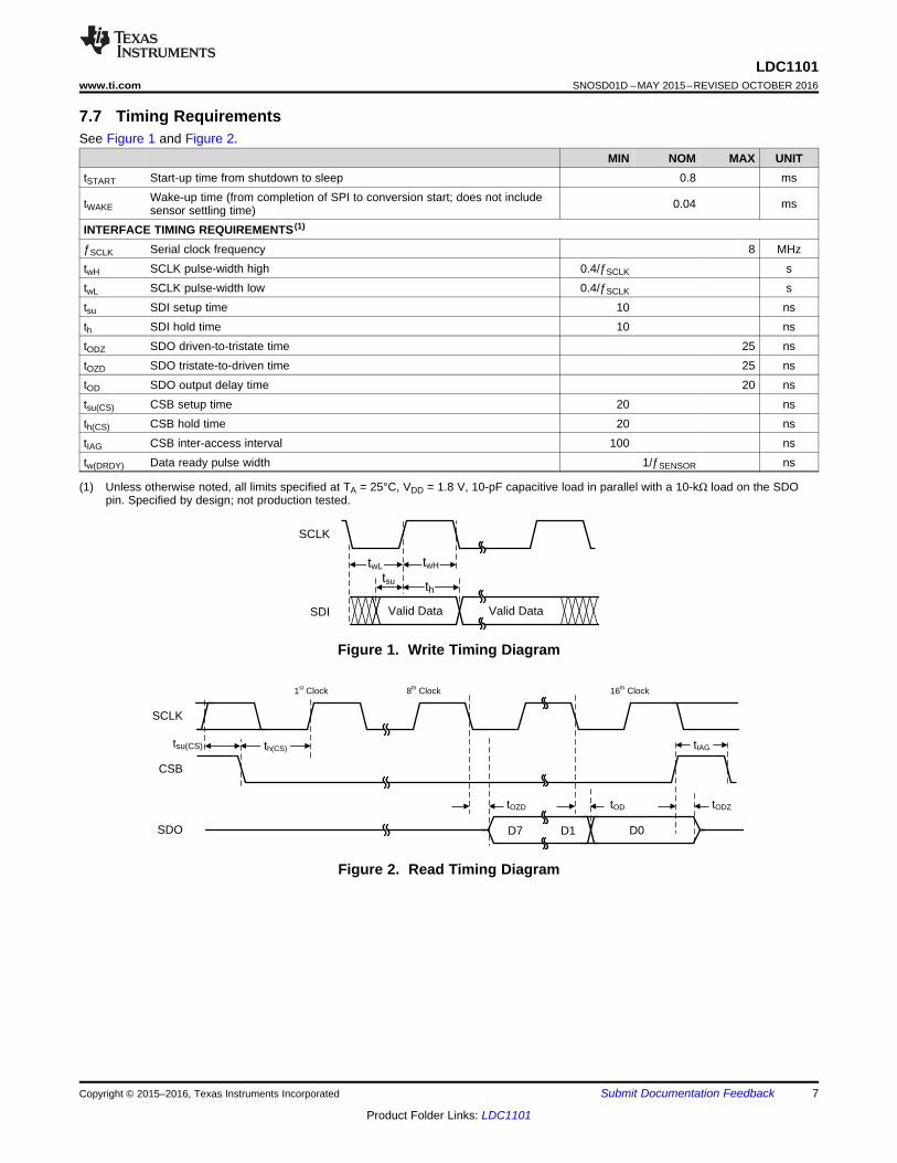
7.7 Timing RequirementsSee Figure 1 and Figure 2.
MIN NOM MAX UNITtSTART Start-up time from shutdown to sleep 0.8 ms
tWAKEWake-up time (from completion of SPI to conversion start; does not includesensor settling time) 0.04 ms
INTERFACE TIMING REQUIREMENTS (1)
ƒSCLK Serial clock frequency 8 MHztwH SCLK pulse-width high 0.4/ƒSCLK stwL SCLK pulse-width low 0.4/ƒSCLK stsu SDI setup time 10 nsth SDI hold time 10 nstODZ SDO driven-to-tristate time 25 nstOZD SDO tristate-to-driven time 25 nstOD SDO output delay time 20 nstsu(CS) CSB setup time 20 nsth(CS) CSB hold time 20 nstIAG CSB inter-access interval 100 nstw(DRDY) Data ready pulse width 1/ƒSENSOR ns
Figure 1. Write Timing Diagram
Figure 2. Read Timing Diagram
VDD (V)
I DD
_LP C
urre
nt (
µA
)
1.7 2 2.3 2.6 2.9 3.2 3.50
50
100
150
200
250
300
D005
-40°C-20°C25°C100°C125°C
Temperature (°C)
I DD
_PD C
urre
nt (
µA
)
-40 0 40 80 1200
2
4
6
8
10
12
14
D006
VDD = 1.8 VVDD = 2.1 VVDD = 2.4 VVDD = 2.7 VVDD = 3.0 VVDD = 3.3 V
Temperature (°C)
I DD
_LP C
urre
nt (
µA
)
-40 0 40 80 1200
50
100
150
200
250
300
D004
VDD = 1.8 VVDD = 2.1 VVDD = 2.4 VVDD = 2.7 VVDD = 3.0 VVDD = 3.3 V
fCLKIN (MHz)
Sup
ply
Cur
rent
(m
A)
8 9 10 11 12 13 14 15 162.95
3
3.05
3.1
3.15
3.2
3.25
3.3
3.35
D003
VDD = 1.8 VVDD = 2.7 VVDD = 3.3 V
Temperature (°C)
I DD C
urre
nt (
mA
)
-40 0 40 80 1201.6
1.7
1.8
1.9
2
2.1
2.2
2.3
2.4
2.5
2.6
D001
VDD = 1.8 VVDD = 2.1 VVDD = 2.4 VVDD = 2.7 VVDD = 3.0 VVDD = 3.3 V
VDD (V)
I DD C
urre
nt (
mA
)
1.7 2 2.3 2.6 2.9 3.2 3.51.4
1.5
1.6
1.7
1.8
1.9
2
2.1
2.2
2.3
2.4
2.5
D002
-40°C-20°C25°C
100°C125°C
8
LDC1101SNOSD01D –MAY 2015–REVISED OCTOBER 2016 www.ti.com
Product Folder Links: LDC1101
Submit Documentation Feedback Copyright © 2015–2016, Texas Instruments Incorporated
7.8 Typical Characteristics
Not including sensor current, default register settings.
Figure 3. IDD vs Temperature
Not including sensor current, default register settings.
Figure 4. IDD vs VDD
Including sensor current. 13-mm diameter sensor 0.1-mmspacing/0.1-mm trace width/ 4-layer 28 turns, fSENSOR = 2 MHz,RP_SET = 0x07, TX1 = 0x50, TC2 = 0x80, RCOUNT = 0xFFFF,
RESP_TIME = 6144
Figure 5. Supply Current (mA) vs ƒCLKIN (MHz) at 25°C Figure 6. IDD Sleep Mode vs Temperature
Figure 7. IDD Sleep Mode vs VDD Figure 8. IDD Shutdown vs Temperature
VDD (V)
I SE
NS
OR (
µA
)
1.7 2 2.3 2.6 2.9 3.2 3.54.6
4.65
4.7
4.75
4.8
D009
-40°C25°C125°C
VDD (V)
I DD
_PD C
urre
nt (
µA
)
1.7 2 2.3 2.6 2.9 3.2 3.50
2
4
6
8
10
12
14
16
D007
-40°C-20°C25°C100°C125°C
VDD (V)
I SE
NS
OR (
µA
)
1.7 2 2.3 2.6 2.9 3.2 3.5590
592
594
596
598
600
602
604
606
608
610
D008
-40°C25°C125°C
9
LDC1101www.ti.com SNOSD01D –MAY 2015–REVISED OCTOBER 2016
Product Folder Links: LDC1101
Submit Documentation FeedbackCopyright © 2015–2016, Texas Instruments Incorporated
Typical Characteristics (continued)
Figure 9. IDD Shutdown vs VDD
RP_SET.RPMIN = b111
Figure 10. ISENSOR-MAX vs VDD
RP_SET.RPMAX = b000
Figure 11. ISENSOR-MIN vs VDD
( )SENSOR
1ƒ Hz
2 L C =
p ´
RP + L Meas
INA
INB
LDC1101VDD
Registers + Logic
GND
SPI
CLKIN
SCLK
CSB
SDO
SDI
High Res L Meas
Sensor Driver
CLDO
ThresholdCompare
10
LDC1101SNOSD01D –MAY 2015–REVISED OCTOBER 2016 www.ti.com
Product Folder Links: LDC1101
Submit Documentation Feedback Copyright © 2015–2016, Texas Instruments Incorporated
8 Detailed Description
8.1 OverviewThe LDC1101 is an inductance-to-digital converter which can simultaneously measure the impedance andresonant frequency of an LC resonator. The high resolution measurement capability enables this device to beused to directly measure changes in physical systems, allowing the resonator to sense the proximity andmovement of conductive materials.
The LDC1101 measures the impedance and resonant frequency by regulating the oscillation amplitude in aclosed-loop configuration at a constant level, while monitoring the energy dissipated by the resonator. Bymonitoring the amount of power injected into the resonator, the LDC1101 can determine the equivalent parallelresistance of the resonator, RP, which it returns as a digital value.
In addition, the LDC1101 device also measures the oscillation frequency of the LC circuit by comparing thesensor frequency to a provided reference frequency. The sensor frequency can then be used to determine theinductance of the LC circuit.
The threshold comparator block can compare the RP+L conversion results versus a programmable threshold.With the threshold registers programmed and comparator enabled, the LDC1101 can provide a switch output,reported as a high/low level on the INTB/SDO pin.
The LDC1101 device supports a wide range of LC combinations with oscillation frequencies ranging from 500kHz to 10 MHz and RP ranging from 1.25 kΩ to 90 kΩ. The device is configured and conversion results retrievedthrough a simple 4-wire SPI. The power supply for the device can range from 1.8 V – 5% to 3.3 V + 5%. Theonly external components necessary for operation are a 15 nF capacitor for internal LDO bypassing and supplybypassing for VDD.
8.2 Functional Block Diagram
8.3 Feature Description
8.3.1 Sensor DriverThe LDC1101 can drive a sensor with a resonant frequency of 500 kHz to 10 MHz with an RP in the range of1.25 kΩ to 90 kΩ. The nominal sensor amplitude is 1.2 V. The sensor Q should be at least 10 for RPmeasurements. The inductive sensor must be connected across the INA and INB pins. The resonant frequencyof the sensor is set by:
where• L is the sensor inductance in Henrys, and• C is the sensor parallel capacitance in Farads. (1)
11
LDC1101www.ti.com SNOSD01D –MAY 2015–REVISED OCTOBER 2016
Product Folder Links: LDC1101
Submit Documentation FeedbackCopyright © 2015–2016, Texas Instruments Incorporated
8.4 Device Functional Modes
8.4.1 Measurement ModesThe LDC1101 features two independent measurement subsystems to measure the impedance and resonantfrequency of an attached sensor. The RP+L subsystem can simultaneously measure the impedance andresonant frequency of an LC resonator, with up to 16 bits of resolution for each parameter. Refer to RP+LMeasurement Mode for more information on the RP+L measurement functionality.
The High Resolution L (LHR) subsystem measures the sensor resonant frequency with up to 24 bits ofresolution. The effective resolution is a function of the sample rate and the reference frequency supplied on theCLKIN pin. Refer to High Resolution L (LHR) Measurement Mode for more information on the LHR measurementfunctionality.
Both measurement subsystems can convert simultaneously but at different sample intervals – the completion ofan RP+L conversion will be asynchronous to the completion of a LHR conversion.
Table 1. Comparison of Measurement ModesRP+L Mode LHR Mode
RP Measurement Resolution 16 bits N/AL Measurement Resolution 16 bits 24 bitsSample Rate configuration Varies with ƒSENSOR, set by RESP_TIME Fixed and set by RCOUNT field and ƒCLKIN
Sample rate at highest resolution (SPS) 244 15.3Maximum Sample Rate (kSPS) 156.25 183.9L Resolution at Maximum Sample rate 6.7 bits 6.5 bitsSwitch Output on SDO/INTB Available for RP or L output code N/A
8.4.2 RP+L Measurement ModeIn RP+L mode, the LDC1101 will simultaneously measure the impedance and resonant frequency of theattached sensor. The device accomplishes this task by regulating the oscillation amplitude in a closed-loopconfiguration to a constant level, while monitoring the energy dissipated by the resonator. By monitoring theamount of power injected into the resonator, the LDC1101 device can determine the value of RP. The devicereturns this value as a digital value which is proportional to RP. In addition, the LDC1101 device can alsomeasure the oscillation frequency of the LC circuit, by counting the number of cycles of a reference frequency.The measured sensor frequency can be used to determine the inductance of the LC circuit.
8.4.2.1 RPMIN and RPMAXThe variation of RP in a given system is typically much smaller than maximum range of 1.25 kΩ to >90 kΩsupported by the LDC1101. To achieve better resolution for systems with smaller RP ranges, the LDC1101device offers a programmable RP range.
The LDC1101 uses adjustable current drives to scale the RP measurement range; by setting a tighter currentrange a higher accuracy RP measurement can be performed. This functionality can be considered as a variablegain amplifier (VGA) front end to an ADC. The current ranges are configured in the RPMIN and RPMAX fields ofregister RP_SET (address 0x01). Refer to LDC1101 RP Configuration for instructions to optimize these settings.
8.4.2.2 Programmable Internal Time ConstantsThe LDC1101 utilizes internal programmable registers to configure time constants necessary for sensoroscillation. These internal time constants must be configured for RP measurements. Refer to Setting InternalTime Constant 1 and Setting Internal Time Constant 2 for instructions on how to configure them for a givensystem.
8.4.2.3 RP+L Mode Measurement Sample RateThe LDC1101 provides an adjustable sample rate for the RP+L conversion, where longer conversion times havehigher resolution. Refer to RP+L Sample Rate Configuration With RESP_TIME for more details.
12
LDC1101SNOSD01D –MAY 2015–REVISED OCTOBER 2016 www.ti.com
Product Folder Links: LDC1101
Submit Documentation Feedback Copyright © 2015–2016, Texas Instruments Incorporated
8.4.3 High Resolution L (LHR) Measurement ModeThe High Resolution L measurement (LHR) subsystem provides a high-resolution inductance (L) measurementof up to 24 bits. This L measurement can be configured to provide a higher resolution measurement than themeasurement returned from the RP+L subsystem. The LHR subsystem also provides a constant conversion timeinterval, whereas the RP+L conversion interval is a function of the sensor frequency. The LHR measurementruns asynchronously with respect to the RP+L measurement. For more information on LHR mode resolution,refer to Optimizing L Measurement Resolution for the LDC161x and LDC1101 (SNOA944).
8.4.4 Reference Count SettingThe LHR sample rate is set by the Reference Count (LHR_RCOUNT) setting (registers 0x30 and 0x31). TheLHR conversion resolution is proportional to the programmed RCOUNT value. With the maximum supported 16-MHz CLKIN input, the LDC1101 conversion interval can be set from 5.44 µs to 65.54 ms in 1-µs increments.Note that longer conversion intervals produce more accurate LHR measurements. Refer to LHR Sample RateConfiguration With RCOUNT for more details.
8.4.5 L-Only Measurement OperationThe LDC1101 can disable the RP measurement to perform a more stable L measurement. To enable this mode,set:• ALT_CONFIG.LOPTIMAL(register 0x05-bit0) = 1• D_CONFIG.DOK_REPORT (register 0x0C-bit0) = 1
When this mode is used, RP measurement results are not valid.
8.4.6 Minimum Sensor Frequency and Watchdog SettingThe LDC1101 can report an error condition if the sensor oscillation stops. Refer to MIN_FREQ and WatchdogConfiguration for information on the configuration of the watchdog.
8.4.7 Low Power ModesWhen continuous LDC conversions are not required, the LDC1101 supports two reduced power modes. In Sleepmode, the LDC1101 retains register settings and can quickly enter active mode for conversions. In Shutdownmode, power consumption is significantly lower, although the device configuration is not retained. While in eitherlow power mode, the LDC1101 does not perform conversions.
8.4.7.1 Shutdown ModeShutdown mode is the lowest power state for the LDC1101. Note that entering SD mode will reset all registers totheir default state, and so the device must have its registers rewritten. To enter Shutdown, perform the followingsequence:1. Set ALT_CONFIG.SHUTDOWN_EN = 1 (register 0x05-bit[1]).2. Stop toggling the CLKIN pin input and drive the CLKIN pin Low.3. Set START_CONFIG.FUNC_MODE = b10 (register 0x0B:bits[1:0]). This register can be written while the
LDC1101 is in active mode; on completion of the register write the LDC1101 will enter shutdown.
To exit Shutdown mode, resume toggling the clock input on the CLKIN pin; the LDC1101 transitions to Sleepmode with the default register values.
While in Shutdown mode, no conversions are performed. In addition, entering Shutdown mode clears the statusregisters; if an error condition is present it is be reported when the device exits Shutdown mode.
8.4.7.2 Sleep ModeSleep mode is entered by setting START_CONFIG.FUNC_MODE =b01 (register 0x0B:bits[1:0]). While in thismode, the register contents are maintained. To exit Sleep mode and start active conversions, setSTART_CONFIG.FUNC_MODE = b00. While in Sleep mode the SPI interface is functional so that register readsand writes can be performed.
On power-up or exiting Shutdown mode, the LDC1101 is in Sleep mode.
13
LDC1101www.ti.com SNOSD01D –MAY 2015–REVISED OCTOBER 2016
Product Folder Links: LDC1101
Submit Documentation FeedbackCopyright © 2015–2016, Texas Instruments Incorporated
Configuring the LDC1101 must be done while the device is in Sleep mode. If a setting on the LDC1101 needs tobe changed, return the device to Sleep mode, change the appropriate register, and then return the LDC1101 toconversion mode. The registers related to INTB reporting can be changed while the LDC1101 is in active mode.Refer to INTB Reporting on SDO for more details.
8.4.8 Status ReportingThe LDC1101 provides 2 status registers, STATUS and LHR_STATUS, to report on the device and sensorcondition.
Table 2. STATUS FieldsNAME FIELD FUNCTION
NO_SENSOR_OSC 7
When the resonance impedance of the sensor, RP, drops below the programed Rp_MIN, the sensoroscillation may stop. This condition is reported by STATUS:NO_SENSOR_OSC (register 0x20-bit7). Thiscondition could occur when a target comes too close to the sensor or if RP_SET:RP_MIN (register 0x01-bits[2:0]) is set too high.
DRDYB 6 RP+L Data Ready - reports completion of RP+L conversion resultsRP_HIN 5
RP+L threshold – refer to Comparator Functionality for detailsRP_HI_LON 4L_HIN 3L_HI_LON 2POR_READ 0 Device in Power-On Reset – device should only be configured when POR_READ = 0.
The LHR_STATUS register (register 0x3B) reports on LHR functionality.
8.4.9 Switch Functionality and INTB ReportingThe SDO pin can generate INTB, a signal which corresponds to device status. INTB can report conversioncompletion or provide a comparator output, in which the LDC conversion results are internally compared toprogrammable thresholds. Refer to INTB Reporting on SDO for details.
8.5 Programming
8.5.1 SPI ProgrammingThe LDC1101 uses SPI to configure the internal registers. It is necessary to configure the LDC1101 while inSleep mode. If a setting on the LDC1101 needs to be changed, return the device to Sleep mode, change theappropriate register, and then return the LDC1101 to conversion mode. CSB must go low before accessing firstaddress. If the number of SCLK pulses is less than 16, a register write command does not change the contentsof the addressed register.
A6 A5 A4 A3 A2 A1 A0 D7 D6 D5 D4 D3 D2 D1
CSB
SCK
COMMAND FIELD DATA FIELD for ADDRESS A
1 2 3 4 5 6 7 8 9 10 11 12 13 14 15 16
LSBMSB
Address (7 bits) Write Data to Address A (8-bits)
SDI
D7 D6 D5 D4 D3 D2 D1
Read Data from Address A (8-bits)
SDO
LSBMSB
__R/W
R/W = Instruction1: Read0: Write
D0
D0 D7 D6 D5 D4 D3 D2 D1
DATA FIELD for ADDRESS A+1
LSBMSB
D0
D7 D6 D5 D4 D3 D2 D1
Read Data from Address A+1 (8-bits)
LSBMSB
D0
17 18 19 20 21 22 23 24
Write Data to Address A+1 (8-bits)
A6 A5 A4 A3 A2 A1 A0 D7 D6 D5 D4 D3 D2 D1
CSB
SCK
tCOMMAND FIELDt tDATA FIELDt
1 2 3 4 5 6 7 8 9 10 11 12 13 14 15 16
LSBMSB
Address (7 bits) Write Data (8-bits)
SDI
D7 D6 D5 D4 D3 D2 D1
Read Data (8-bits)
SDO
LSBMSB
__R/W
R/W = Instruction1: Read0: Write
D0
D0
14
LDC1101SNOSD01D –MAY 2015–REVISED OCTOBER 2016 www.ti.com
Product Folder Links: LDC1101
Submit Documentation Feedback Copyright © 2015–2016, Texas Instruments Incorporated
Programming (continued)
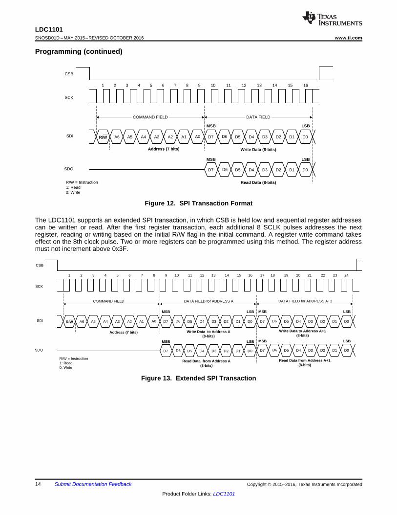
Figure 12. SPI Transaction Format
The LDC1101 supports an extended SPI transaction, in which CSB is held low and sequential register addressescan be written or read. After the first register transaction, each additional 8 SCLK pulses addresses the nextregister, reading or writing based on the initial R/W flag in the initial command. A register write command takeseffect on the 8th clock pulse. Two or more registers can be programmed using this method. The register addressmust not increment above 0x3F.
Figure 13. Extended SPI Transaction
15
LDC1101www.ti.com SNOSD01D –MAY 2015–REVISED OCTOBER 2016
Product Folder Links: LDC1101
Submit Documentation FeedbackCopyright © 2015–2016, Texas Instruments Incorporated
8.6 Register Maps
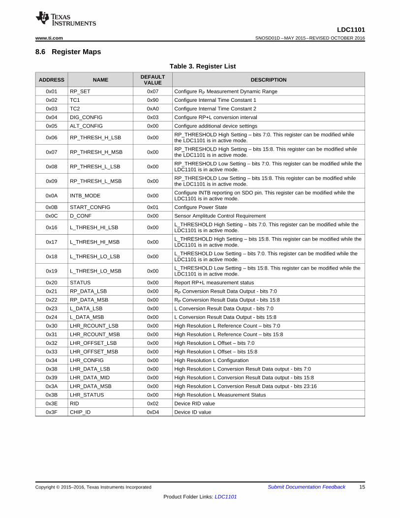
Table 3. Register List
ADDRESS NAME DEFAULTVALUE DESCRIPTION
0x01 RP_SET 0x07 Configure RP Measurement Dynamic Range0x02 TC1 0x90 Configure Internal Time Constant 10x03 TC2 0xA0 Configure Internal Time Constant 20x04 DIG_CONFIG 0x03 Configure RP+L conversion interval0x05 ALT_CONFIG 0x00 Configure additional device settings
0x06 RP_THRESH_H_LSB 0x00 RP_THRESHOLD High Setting – bits 7:0. This register can be modified whilethe LDC1101 is in active mode.
0x07 RP_THRESH_H_MSB 0x00 RP_THRESHOLD High Setting – bits 15:8. This register can be modified whilethe LDC1101 is in active mode.
0x08 RP_THRESH_L_LSB 0x00 RP_THRESHOLD Low Setting – bits 7:0. This register can be modified while theLDC1101 is in active mode.
0x09 RP_THRESH_L_MSB 0x00 RP_THRESHOLD Low Setting – bits 15:8. This register can be modified whilethe LDC1101 is in active mode.
0x0A INTB_MODE 0x00 Configure INTB reporting on SDO pin. This register can be modified while theLDC1101 is in active mode.
0x0B START_CONFIG 0x01 Configure Power State0x0C D_CONF 0x00 Sensor Amplitude Control Requirement
0x16 L_THRESH_HI_LSB 0x00 L_THRESHOLD High Setting – bits 7:0. This register can be modified while theLDC1101 is in active mode.
0x17 L_THRESH_HI_MSB 0x00 L_THRESHOLD High Setting – bits 15:8. This register can be modified while theLDC1101 is in active mode.
0x18 L_THRESH_LO_LSB 0x00 L_THRESHOLD Low Setting – bits 7:0. This register can be modified while theLDC1101 is in active mode.
0x19 L_THRESH_LO_MSB 0x00 L_THRESHOLD Low Setting – bits 15:8. This register can be modified while theLDC1101 is in active mode.
0x20 STATUS 0x00 Report RP+L measurement status0x21 RP_DATA_LSB 0x00 RP Conversion Result Data Output - bits 7:00x22 RP_DATA_MSB 0x00 RP Conversion Result Data Output - bits 15:80x23 L_DATA_LSB 0x00 L Conversion Result Data Output - bits 7:00x24 L_DATA_MSB 0x00 L Conversion Result Data Output - bits 15:80x30 LHR_RCOUNT_LSB 0x00 High Resolution L Reference Count – bits 7:00x31 LHR_RCOUNT_MSB 0x00 High Resolution L Reference Count – bits 15:80x32 LHR_OFFSET_LSB 0x00 High Resolution L Offset – bits 7:00x33 LHR_OFFSET_MSB 0x00 High Resolution L Offset – bits 15:80x34 LHR_CONFIG 0x00 High Resolution L Configuration0x38 LHR_DATA_LSB 0x00 High Resolution L Conversion Result Data output - bits 7:00x39 LHR_DATA_MID 0x00 High Resolution L Conversion Result Data output - bits 15:80x3A LHR_DATA_MSB 0x00 High Resolution L Conversion Result Data output - bits 23:160x3B LHR_STATUS 0x00 High Resolution L Measurement Status0x3E RID 0x02 Device RID value0x3F CHIP_ID 0xD4 Device ID value
16
LDC1101SNOSD01D –MAY 2015–REVISED OCTOBER 2016 www.ti.com
Product Folder Links: LDC1101
Submit Documentation Feedback Copyright © 2015–2016, Texas Instruments Incorporated
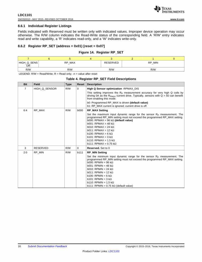
8.6.1 Individual Register ListingsFields indicated with Reserved must be written only with indicated values. Improper device operation may occurotherwise. The R/W column indicates the Read-Write status of the corresponding field. A ‘R/W’ entry indicatesread and write capability, a ‘R’ indicates read-only, and a ‘W’ indicates write-only.
8.6.2 Register RP_SET (address = 0x01) [reset = 0x07]
Figure 14. Register RP_SET
7 6 5 4 3 2 1 0HIGH_Q_SENS
ORRP_MAX RESERVED RP_MIN
R/W R/W R/W R/WLEGEND: R/W = Read/Write; R = Read only; -n = value after reset
Table 4. Register RP_SET Field DescriptionsBit Field Type Reset Description7 HIGH_Q_SENSOR R/W 0 High Q Sensor optimization -RPMAX_DIS
This setting improves the RP measurement accuracy for very high Q coils bydriving 0A as the RPMAX current drive. Typically, sensors with Q > 50 can benefitfrom enabling this mode.b0: Programmed RP_MAX is driven (default value)b1: RP_MAX current is ignored; current drive is off.
6:4 RP_MAX R/W b000 RP_MAX SettingSet the maximum input dynamic range for the sensor RP measurement. Theprogrammed RP_MIN setting must not exceed the programmed RP_MAX setting.b000: RPMAX = 96 kΩ (default value)b001: RPMAX = 48 kΩb010: RPMAX = 24 kΩb011: RPMAX = 12 kΩb100: RPMAX = 6 kΩb101: RPMAX = 3 kΩb110: RPMAX = 1.5 kΩb111: RPMAX = 0.75 kΩ
3 RESERVED R/W 0 Reserved. Set to 02:0 RP_MIN R/W b111 RP_MIN Setting
Set the minimum input dynamic range for the sensor RP measurement. Theprogrammed RP_MIN setting must not exceed the programmed RP_MAX setting.b000: RPMIN = 96 kΩb001: RPMIN = 48 kΩb010: RPMIN = 24 kΩb011: RPMIN = 12 kΩb100: RPMIN = 6 kΩb101: RPMIN = 3 kΩb110: RPMIN = 1.5 kΩb111: RPMIN = 0.75 kΩ (default value)
17
LDC1101www.ti.com SNOSD01D –MAY 2015–REVISED OCTOBER 2016
Product Folder Links: LDC1101
Submit Documentation FeedbackCopyright © 2015–2016, Texas Instruments Incorporated
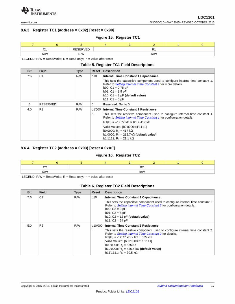
8.6.3 Register TC1 (address = 0x02) [reset = 0x90]
Figure 15. Register TC1
7 6 5 4 3 2 1 0C1 RESERVED R1
R/W R/W R/WLEGEND: R/W = Read/Write; R = Read only; -n = value after reset
Table 5. Register TC1 Field DescriptionsBit Field Type Reset Description7:6 C1 R/W b10 Internal Time Constant 1 Capacitance
This sets the capacitive component used to configure internal time constant 1.Refer to Setting Internal Time Constant 1 for more details.b00: C1 = 0.75 pFb01: C1 = 1.5 pFb10: C1 = 3 pF (default value)b11: C1 = 6 pF
5 RESERVED R/W 0 Reserved. Set to 04:0 R1 R/W b1'000
0Internal Time Constant 1 ResistanceThis sets the resistive component used to configure internal time constant 1.Refer to Setting Internal Time Constant 1 for configuration details.R1(Ω) = –12.77 kΩ × R1 + 417 kΩValid Values: [b0’0000:b1’1111]b0’0000: R1 = 417 kΩb1’0000: R1 = 212.7kΩ (default value)b1’1111: R1 = 21.1 kΩ
8.6.4 Register TC2 (address = 0x03) [reset = 0xA0]
Figure 16. Register TC2
7 6 5 4 3 2 1 0C2 R2
R/W R/WLEGEND: R/W = Read/Write; R = Read only; -n = value after reset
Table 6. Register TC2 Field DescriptionsBit Field Type Reset Description7:6 C2 R/W b10 Internal Time Constant 2 Capacitance
This sets the capacitive component used to configure internal time constant 2.Refer to Setting Internal Time Constant 2 for configuration details.b00: C2 = 3 pFb01: C2 = 6 pFb10: C2 = 12 pF (default value)b11: C2 = 24 pF
5:0 R2 R/W b10'0000
Internal Time Constant 2 ResistanceThis sets the resistive component used to configure internal time constant 2.Refer to Setting Internal Time Constant 2 for details.R2(Ω) = -12.77 kΩ × R2 + 835 kΩValid Values: [b00’0000:b11’1111]b00’0000: R2 = 835kΩb10’0000: R2 = 426.4 kΩ (default value)b11’1111: R2 = 30.5 kΩ
( )SENSOR
Re sponse TimeConversion Time s
3 ƒ=
´
18
LDC1101SNOSD01D –MAY 2015–REVISED OCTOBER 2016 www.ti.com
Product Folder Links: LDC1101
Submit Documentation Feedback Copyright © 2015–2016, Texas Instruments Incorporated
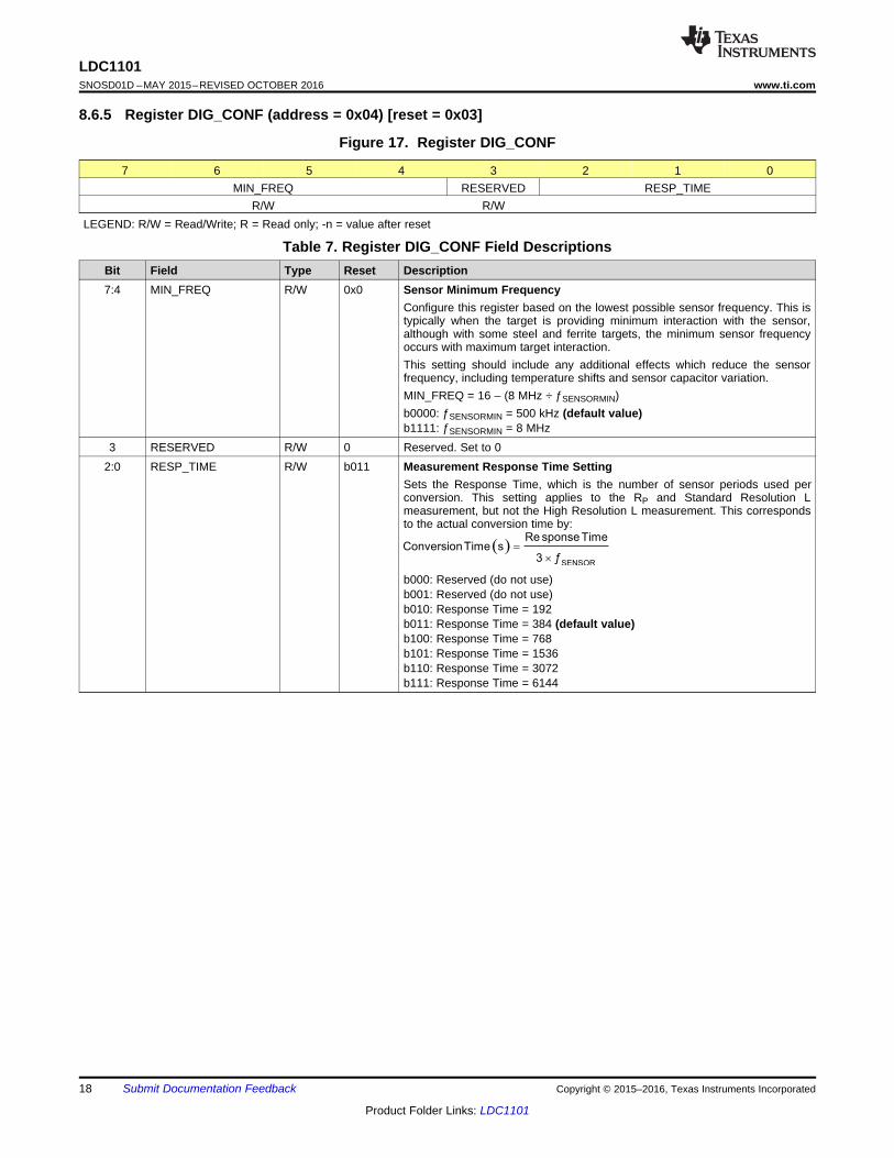
8.6.5 Register DIG_CONF (address = 0x04) [reset = 0x03]
Figure 17. Register DIG_CONF
7 6 5 4 3 2 1 0MIN_FREQ RESERVED RESP_TIME
R/W R/WLEGEND: R/W = Read/Write; R = Read only; -n = value after reset
Table 7. Register DIG_CONF Field DescriptionsBit Field Type Reset Description7:4 MIN_FREQ R/W 0x0 Sensor Minimum Frequency
Configure this register based on the lowest possible sensor frequency. This istypically when the target is providing minimum interaction with the sensor,although with some steel and ferrite targets, the minimum sensor frequencyoccurs with maximum target interaction.This setting should include any additional effects which reduce the sensorfrequency, including temperature shifts and sensor capacitor variation.MIN_FREQ = 16 – (8 MHz ÷ ƒSENSORMIN)b0000: ƒSENSORMIN = 500 kHz (default value)b1111: ƒSENSORMIN = 8 MHz
3 RESERVED R/W 0 Reserved. Set to 02:0 RESP_TIME R/W b011 Measurement Response Time Setting
Sets the Response Time, which is the number of sensor periods used perconversion. This setting applies to the RP and Standard Resolution Lmeasurement, but not the High Resolution L measurement. This correspondsto the actual conversion time by:
b000: Reserved (do not use)b001: Reserved (do not use)b010: Response Time = 192b011: Response Time = 384 (default value)b100: Response Time = 768b101: Response Time = 1536b110: Response Time = 3072b111: Response Time = 6144
19
LDC1101www.ti.com SNOSD01D –MAY 2015–REVISED OCTOBER 2016
Product Folder Links: LDC1101
Submit Documentation FeedbackCopyright © 2015–2016, Texas Instruments Incorporated
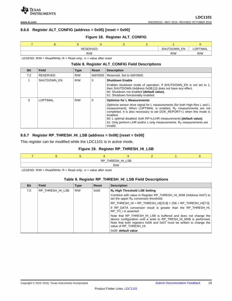
8.6.6 Register ALT_CONFIG (address = 0x05) [reset = 0x00]
Figure 18. Register ALT_CONFIG
7 6 5 4 3 2 1 0RESERVED SHUTDOWN_EN LOPTIMAL
R/W R/W R/WLEGEND: R/W = Read/Write; R = Read only; -n = value after reset
Table 8. Register ALT_CONFIG Field DescriptionsBit Field Type Reset Description7:2 RESERVED R/W b00'0000 Reserved. Set to b00'0000.1 SHUTDOWN_EN R/W 0 Shutdown Enable
Enables shutdown mode of operation. If SHUTDOWN_EN is not set to 1,then SHUTDOWN (Address 0x0B:[1]) does not have any effect.b0: Shutdown not enabled (default value).b1: Shutdown functionality enabled.
0 LOPTIMAL R/W 0 Optimize for L MeasurementsOptimize sensor drive signal for L measurements (for both High-Res L and Lmeasurement). When LOPTIMAL is enabled, RP measurements are notcompleted. It is also necessary to set DOK_REPORT=1 when this mode isenabled.b0: L optimal disabled; both RP+L/LHR measurements (default value).b1: Only perform LHR and/or L-only measurements. RP measurements areinvalid.
8.6.7 Register RP_THRESH_HI_LSB (address = 0x06) [reset = 0x00]This register can be modified while the LDC1101 is in active mode.
Figure 19. Register RP_THRESH_HI_LSB
7 6 5 4 3 2 1 0RP_THRESH_HI_LSB
R/WLEGEND: R/W = Read/Write; R = Read only; -n = value after reset
Table 9. Register RP_THRESH_HI_LSB Field DescriptionsBit Field Type Reset Description7:0 RP_THRESH_HI_LSB R/W 0x00 RP High Threshold LSB Setting
Combine with value in Register RP_THRESH_HI_MSB (Address 0x07) toset the upper RP conversion threshold:RP_THRESH_HI = RP_THRESH_HI[15:8] × 256 + RP_THRESH_HI[7:0]If RP_DATA conversion result is greater than the RP_THRESH_HI,RP_TH_I is asserted.Note that RP_THRESH_HI_LSB is buffered and does not change thedevice configuration until a write to RP_TRESH_HI_MSB is performed.Note that both registers 0x06 and 0x07 must be written to change thevalue of RP_THRESH_HI.0x00: default value
20
LDC1101SNOSD01D –MAY 2015–REVISED OCTOBER 2016 www.ti.com
Product Folder Links: LDC1101
Submit Documentation Feedback Copyright © 2015–2016, Texas Instruments Incorporated
8.6.8 Register RP_THRESH_HI_MSB (address = 0x07) [reset = 0x00]This register can be modified while the LDC1101 is in active mode.
Figure 20. Register RP_THRESH_HI_MSB
7 6 5 4 3 2 1 0RP_THRESH_HI_MSB
R/WLEGEND: R/W = Read/Write; R = Read only; -n = value after reset
Table 10. Register RP_THRESH_HI_MSB Field DescriptionsBit Field Type Reset Description7:0 RP_THRESH_HI_MSB R/W 0x00 RP High Threshold MSB Setting
Combine with value in Register RP_THRESH_HI_LSB (Address 0x06) toset the upper RP conversion threshold.0x00: default value
8.6.9 Register RP_THRESH_LO_LSB (address = 0x08) [reset = 0x00]This register can be modified while the LDC1101 is in active mode.
Figure 21. Register RP_THRESH_LO_LSB
7 6 5 4 3 2 1 0RP_THRESH_LO_LSB
R/WLEGEND: R/W = Read/Write; R = Read only; -n = value after reset
Table 11. Register RP_THRESH_LO_LSB Field DescriptionsBit Field Type Reset Description7:0 RP_THRESH_LO[7:0] R/W 0x00 RP Low Threshold LSB Setting
Combine with value in Register RP_THRESH_LO_MSB (Address 0x09)to set the lower RP conversion threshold:RP_THRESH_LO = RP_THRESH_LO[15:8] ×256 +RP_THRESH_LO[7:0]If RP_DATA conversion result is less than the RP_THRESH_LO,RP_HI_LON is asserted. Note that RP_THRESH_LO_LSB is bufferedand does not change the device configuration until a write toRP_TRESH_LO_MSB is performed.Note that both registers 0x08 and 0x09 must be written to change thevalue of RP_THRESH_LO.0x00: default value
8.6.10 Register RP_THRESH_LO_MSB (address = 0x09) [reset = 0x00]This register can be modified while the LDC1101 is in active mode
Figure 22. Register RP_THRESH_LO_MSB
7 6 5 4 3 2 1 0RP_THRESH_LO_MSB
R/WLEGEND: R/W = Read/Write; R = Read only; -n = value after reset
Table 12. Register RP_THRESH_LO_MSB Field DescriptionsBit Field Type Reset Description7:0 RP_THRESH_LO_MSB[1
5:8]R/W 0x00 RP Low Threshold MSB Setting
Combine with value in Register RP_THRESH_LO_LSB (Address 0x08)to set the lower RP conversion threshold.0x00: default value
21
LDC1101www.ti.com SNOSD01D –MAY 2015–REVISED OCTOBER 2016
Product Folder Links: LDC1101
Submit Documentation FeedbackCopyright © 2015–2016, Texas Instruments Incorporated
8.6.11 Register INTB_MODE (address = 0x0A) [reset = 0x00]This register can be modified while the LDC1101 is in active mode.
Figure 23. Register INTB_MODE
7 6 5 4 3 2 1 0INTB2SDO RESERVED INTB_FUNC
R/W R/W R/WLEGEND: R/W = Read/Write; R = Read only; -n = value after reset
Table 13. INTB_MODE Field DescriptionsBit Field Type Reset Description7 INTB2SDO R/W 0 INTB Output on SDO
Output INTB signal on SDO pin.b0: do not report INTB on SDO pin (default value)b1: report INTB on SDO pin
6 RESERVED R/W 0 Reserved. Set to 05:0 INTB_FUNC R/W b00'0000 Select INTB signal reporting. INTB2SDO must be set to 1 for the
selected signal to appear on the SDO pin. Refer to INTB Reporting onSDO for configuration details.b10’0000: Report LHR Data Readyb01’0000: Compare L conversion to L Thresholds (hysteresis)b00’1000: Compare L conversion to L High Threshold (latching)b00’0100: Report RP+L Data Readyb00’0010: Compare RP conversion to RP Thresholds (hysteresis)b00’0001: Compare RP conversion to RP High Threshold (latching)b00’0000: no output (default value)All other values: Reserved
8.6.12 9.Register START_CONFIG (address = 0x0B) [reset = 0x01]This register can be modified while the LDC1101 is in active mode.
Figure 24. Register START_CONFIG
7 6 5 4 3 2 1 0RESERVED FUNC_MODE
R/W R/WLEGEND: R/W = Read/Write; R = Read only; -n = value after reset
Table 14. Register START_CONFIG Field DescriptionsBit Field Type Reset Description7:2 RESERVED R/W b00'0000 Reserved. Set to b00’00001:0 FUNC_MODE R/W b01 Functional Mode
Configure functional mode of device. In active mode, the deviceperforms conversions. When in Sleep mode, the LDC1101 is in areduced power mode; the device should be configured in this mode.Shutdown mode is a minimal current mode in which the deviceconfiguration is not retained.Note that SHUTDOWN_EN must be set to 1 prior to settingFUNC_MODE to b10.b00: Active conversion modeb01: Sleep mode (default value)b10: Set device to shutdown modeb11: Reserved
22
LDC1101SNOSD01D –MAY 2015–REVISED OCTOBER 2016 www.ti.com
Product Folder Links: LDC1101
Submit Documentation Feedback Copyright © 2015–2016, Texas Instruments Incorporated
8.6.13 Register D_CONFIG (address = 0x0C) [reset = 0x00]
Figure 25. Register D_CONFIG
7 6 5 4 3 2 1 0RESERVED DOK_REPORT
R/W R/WLEGEND: R/W = Read/Write; R = Read only; -n = value after reset
Table 15. Register D_CONFIG Field DescriptionsBit Field Type Reset Description7:1 RESERVED R/W b000'0000 Reserved.
Set to b000’0000.0 DOK_REPORT R/W 0 Sensor Amplitude Control
Continue to convert even if sensor amplitude is not regulated.b0: Require amplitude regulation for conversion (default value)b1: LDC continues to convert even if sensor amplitude is unable tomaintain regulation.
8.6.14 Register L_THRESH_HI_LSB (address = 0x16) [reset = 0x00]This register can be modified while the LDC1101 is in active mode.
Figure 26. Register L_THRESH_HI_LSB
7 6 5 4 3 2 1 0L_THRESH_HI[7:0]
R/WLEGEND: R/W = Read/Write; R = Read only; -n = value after reset
Table 16. Register L_THRESH_HI_LSB Field DescriptionsBit Field Type Reset Description7:0 L_THRESH_HI[7:0] R/W 0x00 L High Threshold LSB Setting
Combine with value in Register L_THRESH_HI_MSB (Address 0x17) toset the upper L conversion threshold:LThreshHI = L_THRESH_HI[15:8] ×256 + L_THRESH_HI[7:0]If L_DATA conversion result is greater than the L_THRESH_HI, L_HINis asserted. Note that L_THRESH_HI_LSB is buffered and does notchange the device configuration until a write to L_TRESH_HI_MSB.0x00: default value
8.6.15 Register L_THRESH_HI_MSB (address = 0x17) [reset = 0x00]This register can be modified while the LDC1101 is in active mode.
Figure 27. Register L_THRESH_HI_MSB
7 6 5 4 3 2 1 0L_THRESH_HI[15:8]
R/WLEGEND: R/W = Read/Write; R = Read only; -n = value after reset
Table 17. Register L_THRESH_HI_MSB Field DescriptionsBit Field Type Reset Description7:0 L_THRESH_HI[15:8] R/W 0x00 L High Threshold MSB Setting
Combine with value in Register L_THRESH_HI_LSB (Address 0x16)to set the upper L conversion threshold.0x00: default value
23
LDC1101www.ti.com SNOSD01D –MAY 2015–REVISED OCTOBER 2016
Product Folder Links: LDC1101
Submit Documentation FeedbackCopyright © 2015–2016, Texas Instruments Incorporated
8.6.16 Register L_THRESH_LO_LSB (address = 0x18) [reset = 0x00]This register can be modified while the LDC1101 is in active mode.
Figure 28. Register L_THRESH_LO_LSB
7 6 5 4 3 2 1 0L_THRESH_L[7:0]
R/WLEGEND: R/W = Read/Write; R = Read only; -n = value after reset
Table 18. Register L_THRESH_LO_LSB Field DescriptionsBit Field Type Reset Description7:0 L_THRESH_LO[7:0] R/W 0x00 L Low Threshold LSB Setting
Combine with value in Register L_THRESH_LO_MSB (Address0x19) to set the lower L conversion threshold:LThreshLO = L_THRESH_LO[15:8] ×256 + L_THRESH_LO[7:0]If L_DATA conversion result is less than the L_THRESH_LO,L_HI_LON is asserted.Note that L_THRESH_LO_LSB is buffered and does not change thedevice configuration until a write to L_TRESH_LO_MSB.0x00: default value
8.6.17 Register L_THRESH_LO_MSB (address = 0x19) [reset = 0x00]This register can be modified while the LDC1101 is in active mode.
Figure 29. L_THRESH_LO_MSB
7 6 5 4 3 2 1 0L_THRESH_L[15:8]
R/WLEGEND: R/W = Read/Write; R = Read only; -n = value after reset
Table 19. L_THRESH_LO_MSB Field DescriptionsBit Field Type Reset Description7:0 L_THRESH_LO[15:8] R/W 0x00 L Low Threshold MSB Setting
Combine with value in Register L_THRESH_LO_LSB (Address0x18) to set the lower L conversion threshold.0x00: default value
24
LDC1101SNOSD01D –MAY 2015–REVISED OCTOBER 2016 www.ti.com
Product Folder Links: LDC1101
Submit Documentation Feedback Copyright © 2015–2016, Texas Instruments Incorporated
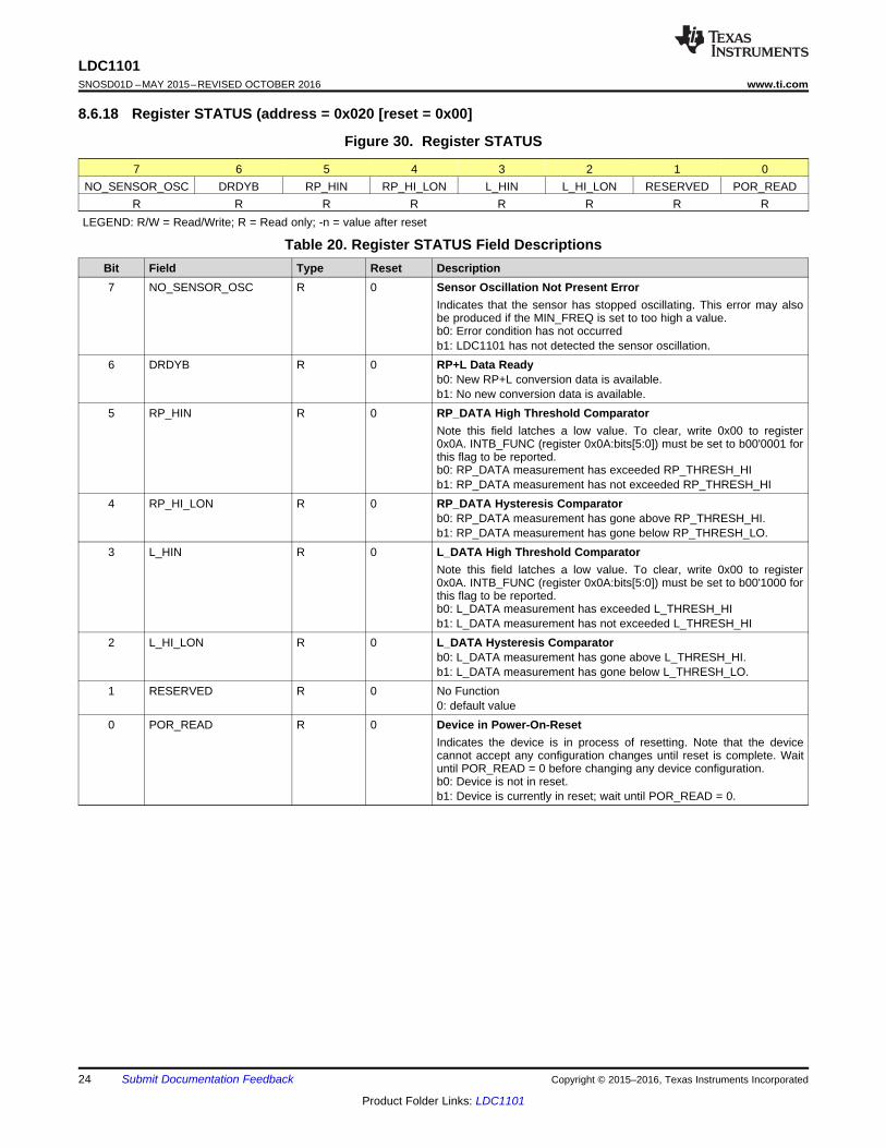
8.6.18 Register STATUS (address = 0x020 [reset = 0x00]
Figure 30. Register STATUS
7 6 5 4 3 2 1 0NO_SENSOR_OSC DRDYB RP_HIN RP_HI_LON L_HIN L_HI_LON RESERVED POR_READ
R R R R R R R RLEGEND: R/W = Read/Write; R = Read only; -n = value after reset
Table 20. Register STATUS Field DescriptionsBit Field Type Reset Description7 NO_SENSOR_OSC R 0 Sensor Oscillation Not Present Error
Indicates that the sensor has stopped oscillating. This error may alsobe produced if the MIN_FREQ is set to too high a value.b0: Error condition has not occurredb1: LDC1101 has not detected the sensor oscillation.
6 DRDYB R 0 RP+L Data Readyb0: New RP+L conversion data is available.b1: No new conversion data is available.
5 RP_HIN R 0 RP_DATA High Threshold ComparatorNote this field latches a low value. To clear, write 0x00 to register0x0A. INTB_FUNC (register 0x0A:bits[5:0]) must be set to b00'0001 forthis flag to be reported.b0: RP_DATA measurement has exceeded RP_THRESH_HIb1: RP_DATA measurement has not exceeded RP_THRESH_HI
4 RP_HI_LON R 0 RP_DATA Hysteresis Comparatorb0: RP_DATA measurement has gone above RP_THRESH_HI.b1: RP_DATA measurement has gone below RP_THRESH_LO.
3 L_HIN R 0 L_DATA High Threshold ComparatorNote this field latches a low value. To clear, write 0x00 to register0x0A. INTB_FUNC (register 0x0A:bits[5:0]) must be set to b00'1000 forthis flag to be reported.b0: L_DATA measurement has exceeded L_THRESH_HIb1: L_DATA measurement has not exceeded L_THRESH_HI
2 L_HI_LON R 0 L_DATA Hysteresis Comparatorb0: L_DATA measurement has gone above L_THRESH_HI.b1: L_DATA measurement has gone below L_THRESH_LO.
1 RESERVED R 0 No Function0: default value
0 POR_READ R 0 Device in Power-On-ResetIndicates the device is in process of resetting. Note that the devicecannot accept any configuration changes until reset is complete. Waituntil POR_READ = 0 before changing any device configuration.b0: Device is not in reset.b1: Device is currently in reset; wait until POR_READ = 0.
25
LDC1101www.ti.com SNOSD01D –MAY 2015–REVISED OCTOBER 2016
Product Folder Links: LDC1101
Submit Documentation FeedbackCopyright © 2015–2016, Texas Instruments Incorporated
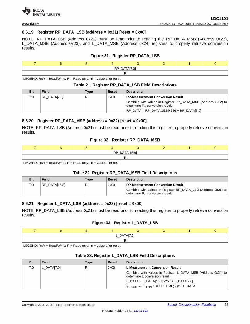
8.6.19 Register RP_DATA_LSB (address = 0x21) [reset = 0x00]NOTE: RP_DATA_LSB (Address 0x21) must be read prior to reading the RP_DATA_MSB (Address 0x22),L_DATA_MSB (Address 0x23), and L_DATA_MSB (Address 0x24) registers to properly retrieve conversionresults.
Figure 31. Register RP_DATA_LSB
7 6 5 4 3 2 1 0RP_DATA[7:0]
RLEGEND: R/W = Read/Write; R = Read only; -n = value after reset
Table 21. Register RP_DATA_LSB Field DescriptionsBit Field Type Reset Description7:0 RP_DATA[7:0] R 0x00 RP-Measurement Conversion Result
Combine with values in Register RP_DATA_MSB (Address 0x22) todetermine RP conversion result:RP_DATA = RP_DATA[15:8]×256 + RP_DATA[7:0]
8.6.20 Register RP_DATA_MSB (address = 0x22) [reset = 0x00]NOTE: RP_DATA_LSB (Address 0x21) must be read prior to reading this register to properly retrieve conversionresults.
Figure 32. Register RP_DATA_MSB
7 6 5 4 3 2 1 0RP_DATA[15:8]
RLEGEND: R/W = Read/Write; R = Read only; -n = value after reset
Table 22. Register RP_DATA_MSB Field DescriptionsBit Field Type Reset Description7:0 RP_DATA[15:8] R 0x00 RP-Measurement Conversion Result
Combine with values in Register RP_DATA_LSB (Address 0x21) todetermine RP conversion result:
8.6.21 Register L_DATA_LSB (address = 0x23) [reset = 0x00]NOTE: RP_DATA_LSB (Address 0x21) must be read prior to reading this register to properly retrieve conversionresults.
Figure 33. Register L_DATA_LSB
7 6 5 4 3 2 1 0L_DATA[7:0]
RLEGEND: R/W = Read/Write; R = Read only; -n = value after reset
Table 23. Register L_DATA_LSB Field DescriptionsBit Field Type Reset Description7:0 L_DATA[7:0] R 0x00 L-Measurement Conversion Result
Combine with values in Register L_DATA_MSB (Address 0x24) todetermine L conversion result:L_DATA = L_DATA[15:8]×256 + L_DATA[7:0]fSENSOR = ( fCLKIN ˣ RESP_TIME) / (3 ˣ L_DATA)
26
LDC1101SNOSD01D –MAY 2015–REVISED OCTOBER 2016 www.ti.com
Product Folder Links: LDC1101
Submit Documentation Feedback Copyright © 2015–2016, Texas Instruments Incorporated
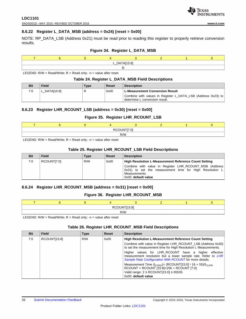
8.6.22 Register L_DATA_MSB (address = 0x24) [reset = 0x00]NOTE: RP_DATA_LSB (Address 0x21) must be read prior to reading this register to properly retrieve conversionresults.
Figure 34. Register L_DATA_MSB
7 6 5 4 3 2 1 0L_DATA[15:8]
RLEGEND: R/W = Read/Write; R = Read only; -n = value after reset
Table 24. Register L_DATA_MSB Field DescriptionsBit Field Type Reset Description7:0 L_DATA[15:8] R 0x00 L-Measurement Conversion Result
Combine with values in Register L_DATA_LSB (Address 0x23) todetermine L conversion result.
8.6.23 Register LHR_RCOUNT_LSB (address = 0x30) [reset = 0x00]
Figure 35. Register LHR_RCOUNT_LSB
7 6 5 4 3 2 1 0RCOUNT[7:0]
R/WLEGEND: R/W = Read/Write; R = Read only; -n = value after reset
Table 25. Register LHR_RCOUNT_LSB Field DescriptionsBit Field Type Reset Description7:0 RCOUNT[7:0] R/W 0x00 High Resolution L-Measurement Reference Count Setting
Combine with value in Register LHR_RCOUNT_MSB (Address0x31) to set the measurement time for High Resolution LMeasurements.0x00: default value
8.6.24 Register LHR_RCOUNT_MSB (address = 0x31) [reset = 0x00]
Figure 36. Register LHR_RCOUNT_MSB
7 6 5 4 3 2 1 0RCOUNT[15:8]
R/WLEGEND: R/W = Read/Write; R = Read only; -n = value after reset
Table 26. Register LHR_RCOUNT_MSB Field DescriptionsBit Field Type Reset Description7:0 RCOUNT[15:8] R/W 0x00 High Resolution L-Measurement Reference Count Setting
Combine with value in Register LHR_RCOUNT_LSB (Address 0x30)to set the measurement time for High Resolution L Measurements.Higher values for LHR_RCOUNT have a higher effectivemeasurement resolution but a lower sample rate. Refer to LHRSample Rate Configuration With RCOUNT for more details.Measurement Time (tCONV)= (RCOUNT[15:0] ˣ 16 + 55)/fCLKINRCOUNT = RCOUNT [15:8]×256 + RCOUNT [7:0]Valid range: 2 ≤ RCOUNT[15:0] ≤ 655350x00: default value
27
LDC1101www.ti.com SNOSD01D –MAY 2015–REVISED OCTOBER 2016
Product Folder Links: LDC1101
Submit Documentation FeedbackCopyright © 2015–2016, Texas Instruments Incorporated
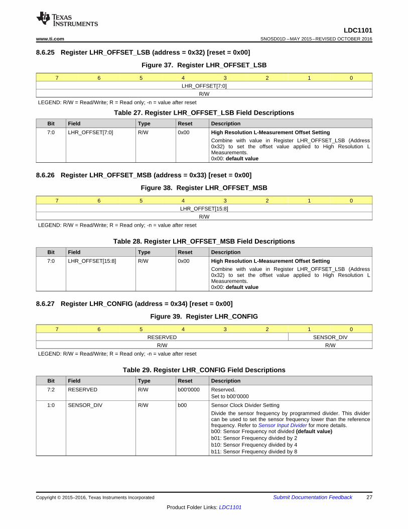
8.6.25 Register LHR_OFFSET_LSB (address = 0x32) [reset = 0x00]
Figure 37. Register LHR_OFFSET_LSB
7 6 5 4 3 2 1 0LHR_OFFSET[7:0]
R/WLEGEND: R/W = Read/Write; R = Read only; -n = value after reset
Table 27. Register LHR_OFFSET_LSB Field DescriptionsBit Field Type Reset Description7:0 LHR_OFFSET[7:0] R/W 0x00 High Resolution L-Measurement Offset Setting
Combine with value in Register LHR_OFFSET_LSB (Address0x32) to set the offset value applied to High Resolution LMeasurements.0x00: default value
8.6.26 Register LHR_OFFSET_MSB (address = 0x33) [reset = 0x00]
Figure 38. Register LHR_OFFSET_MSB
7 6 5 4 3 2 1 0LHR_OFFSET[15:8]
R/WLEGEND: R/W = Read/Write; R = Read only; -n = value after reset
Table 28. Register LHR_OFFSET_MSB Field DescriptionsBit Field Type Reset Description7:0 LHR_OFFSET[15:8] R/W 0x00 High Resolution L-Measurement Offset Setting
Combine with value in Register LHR_OFFSET_LSB (Address0x32) to set the offset value applied to High Resolution LMeasurements.0x00: default value
8.6.27 Register LHR_CONFIG (address = 0x34) [reset = 0x00]
Figure 39. Register LHR_CONFIG
7 6 5 4 3 2 1 0RESERVED SENSOR_DIV
R/W R/WLEGEND: R/W = Read/Write; R = Read only; -n = value after reset
Table 29. Register LHR_CONFIG Field DescriptionsBit Field Type Reset Description7:2 RESERVED R/W b00'0000 Reserved.
Set to b00’00001:0 SENSOR_DIV R/W b00 Sensor Clock Divider Setting
Divide the sensor frequency by programmed divider. This dividercan be used to set the sensor frequency lower than the referencefrequency. Refer to Sensor Input Divider for more details.b00: Sensor Frequency not divided (default value)b01: Sensor Frequency divided by 2b10: Sensor Frequency divided by 4b11: Sensor Frequency divided by 8
28
LDC1101SNOSD01D –MAY 2015–REVISED OCTOBER 2016 www.ti.com
Product Folder Links: LDC1101
Submit Documentation Feedback Copyright © 2015–2016, Texas Instruments Incorporated
8.6.28 Register LHR_DATA_LSB (address = 0x38) [reset = 0x00]NOTE: The LHR_DATA_X registers must be read in the sequence LHR_DATA_LSB (Address 0x38) first, thenLHR_DATA_MID (Address 0x39), and last LHR_DATA_MSB (Address 0x3A) to ensure correct data.
Figure 40. Register LHR_DATA_LSB
7 6 5 4 3 2 1 0LHR_DATA[7:0]
RLEGEND: R/W = Read/Write; R = Read only; -n = value after reset
Table 30. Register LHR_DATA_LSB Field DescriptionsBit Field Type Reset Description7:0 LHR_DATA[7:0] R 0x00 High Resolution L-Measurement Conversion Result
Combine with values in Registers LHR_DATA_MID (Address 0x39)and LHR_DATA_MSB (Address 0x3A) to determine conversionresult. When LHR_OFFSET =0x0000, ƒSENSOR can be determinedby: ƒSENSOR = ƒCLKIN × 2SENSOR_DIV × LHR_DATA ÷ 224
8.6.29 Register LHR_DATA_MID (address = 0x39) [reset = 0x00]NOTE: The LHR_DATA_X registers must be read in the sequence LHR_DATA_LSB (Address 0x38) first, thenLHR_DATA_MID (Address 0x39), and last LHR_DATA_MSB (Address 0x3A) to ensure correct data.
Figure 41. Register LHR_DATA_MID
7 6 5 4 3 2 1 0LHR_DATA[15:8]
RLEGEND: R/W = Read/Write; R = Read only; -n = value after reset
Table 31. Register LHR_DATA_MID Field DescriptionsBit Field Type Reset Description7:0 LHR_DATA[15:8] R 0x00 High Resolution L-Measurement Conversion Result
Combine with values in Registers LHR_DATA_LSB (Address 0x38)and LHR_DATA_MSB (Address 0x3A) to determine conversionresult.
8.6.30 Register LHR_DATA_MSB (address = 0x3A) [reset = 0x00]NOTE: The LHR_DATA_X registers must be read in the sequence LHR_DATA_LSB (Address 0x38) first, thenLHR_DATA_MID (Address 0x39), and last LHR_DATA_MSB (Address 0x3A) to ensure correct data.
Figure 42. Register LHR_DATA_MSB
7 6 5 4 3 2 1 0LHR_DATA[23:16]
RLEGEND: R/W = Read/Write; R = Read only; -n = value after reset
Table 32. Register LHR_DATA_MSB Field DescriptionsBit Field Type Reset Description7:0 LHR_DATA[23:16] R 0x00 High Resolution L-Measurement Conversion Result
Combine with values in Registers LHR_DATA_LSB (Address 0x38)and LHR_DATA_MID (Address 0x39) to determine conversion result.
29
LDC1101www.ti.com SNOSD01D –MAY 2015–REVISED OCTOBER 2016
Product Folder Links: LDC1101
Submit Documentation FeedbackCopyright © 2015–2016, Texas Instruments Incorporated
8.6.31 Register LHR_STATUS (address = 0x3B) [reset = 0x00]
Figure 43. Register LHR_STATUS
7 6 5 4 3 2 1 0UNUSED ERR_ZC ERR_OR ERR_UR ERR_OF LHR_DRDY
R R R R R RLEGEND: R/W = Read/Write; R = Read only; -n = value after reset
Table 33. Register LHR_STATUS Field DescriptionsBit Field Type Reset Description7:5 UNUSED R 0 No Function4 ERR_ZC R 0 Zero Count Error
Zero count errors are applicable for LHR measurements and indicatethat no cycles of the sensor occurred in the programmed measurementinterval. This indicates either a sensor error or the sensor frequency istoo low. This field is updated after register 0x38 has been read.b0: No Zero Count error has occurred for the last LHR conversion resultread.b1: A Zero Count error has occurred.
3 ERR_OR R 0 Conversion Over-range ErrorConversion over-range errors are applicable for LHR measurements andindicate that the sensor frequency exceeded the reference frequency.This field is updated after register 0x38 has been read.b0: No Conversion Over-range error has occurred for the last LHRconversion result read.b1: A Conversion Over-range error has occurred.
2 ERR_UR R 0 Conversion Under-range ErrorConversion under-range errors are applicable for LHR measurementsand indicate that the output code is negative; this occurs whenprogrammed LHR offset register value is too large. This field is updatedafter register 0x38 has been read.b0: No Conversion Under-range error has occurred for the last LHRconversion result read.b1: A Conversion Under-range error has occurred.
1 ERR_OF R 0 Conversion Over-flow ErrorConversion over-flow errors are applicable for LHR measurements andindicate that the sensor frequency is too close to the referencefrequency. This field is updated after register 0x38 has been read.b0: No Conversion Over-flow error has occurred for the last LHRconversion result read.b1: A Conversion Over-flow error has occurred.
0 LHR_DRDY R 0 LHR Data Readyb0: Unread LHR conversion data is available. This field is set to 0 at theend of an LHR conversion and remains asserted until a read of register0x38.b1: No unread LHR conversion data is available.
30
LDC1101SNOSD01D –MAY 2015–REVISED OCTOBER 2016 www.ti.com
Product Folder Links: LDC1101
Submit Documentation Feedback Copyright © 2015–2016, Texas Instruments Incorporated
8.6.32 Register RID (address = 0x3E) [reset = 0x02]
Figure 44. Register RID
7 6 5 4 3 2 1 0V_ID RID
R RLEGEND: R/W = Read/Write; R = Read only; -n = value after reset
Table 34. Register RID Field DescriptionsBit Field Type Reset Description7:3 V_ID R b00'0000 DEVICE ID
Returns fixed value indicating device ID.b0'0000: indicates LDC1101 (default value)
2:0 RID R b010 RIDReturns device RID.b010: Default value
8.6.33 Register DEVICE_ID (address = 0x3F) [reset = 0xD4]
Figure 45. Register DEVICE_ID
7 6 5 4 3 2 1 0CHIP_ID
RLEGEND: R/W = Read/Write; R = Read only; -n = value after reset
Table 35. Register DEVICE_ID Field DescriptionsBit Field Type Reset Description7:0 CHIP_ID R 0xD4 CHIP_ID
Returns fixed value indicating device Family ID.0xD4: indicates LDC1101 family (default value)
L
RS
C¦
1
2 LC
S
d
Conductive Target
EddyCurrent
31
LDC1101www.ti.com SNOSD01D –MAY 2015–REVISED OCTOBER 2016
Product Folder Links: LDC1101
Submit Documentation FeedbackCopyright © 2015–2016, Texas Instruments Incorporated
9 Application and Implementation
NOTEInformation in the following applications sections is not part of the TI componentspecification, and TI does not warrant its accuracy or completeness. TI’s customers areresponsible for determining suitability of components for their purposes. Customers shouldvalidate and test their design implementation to confirm system functionality.
9.1 Application Information
9.1.1 TI Designs and Application NotesThe following resources contain additional information on LDC1101 operation, configuration, and system design:• Inductive Linear Position Sensing Using the LDC1101• Inductive Proximity Switch Using the LDC1101• LDC Selection Guide Application Report• LDC Sensor Design Application Report• LDC Target Design Application Report• Performing L Measurements from LDC DRDY Timing Application Report• Optimizing L Measurement Resolution for the LDC161x and LDC1101 Application Report• Measuring RP of an L-C Sensor for Inductive Sensing Application Report• Setting LDC1312/4, LDC1612/4, and LDC1101 Sensor Drive Configuration Application Report
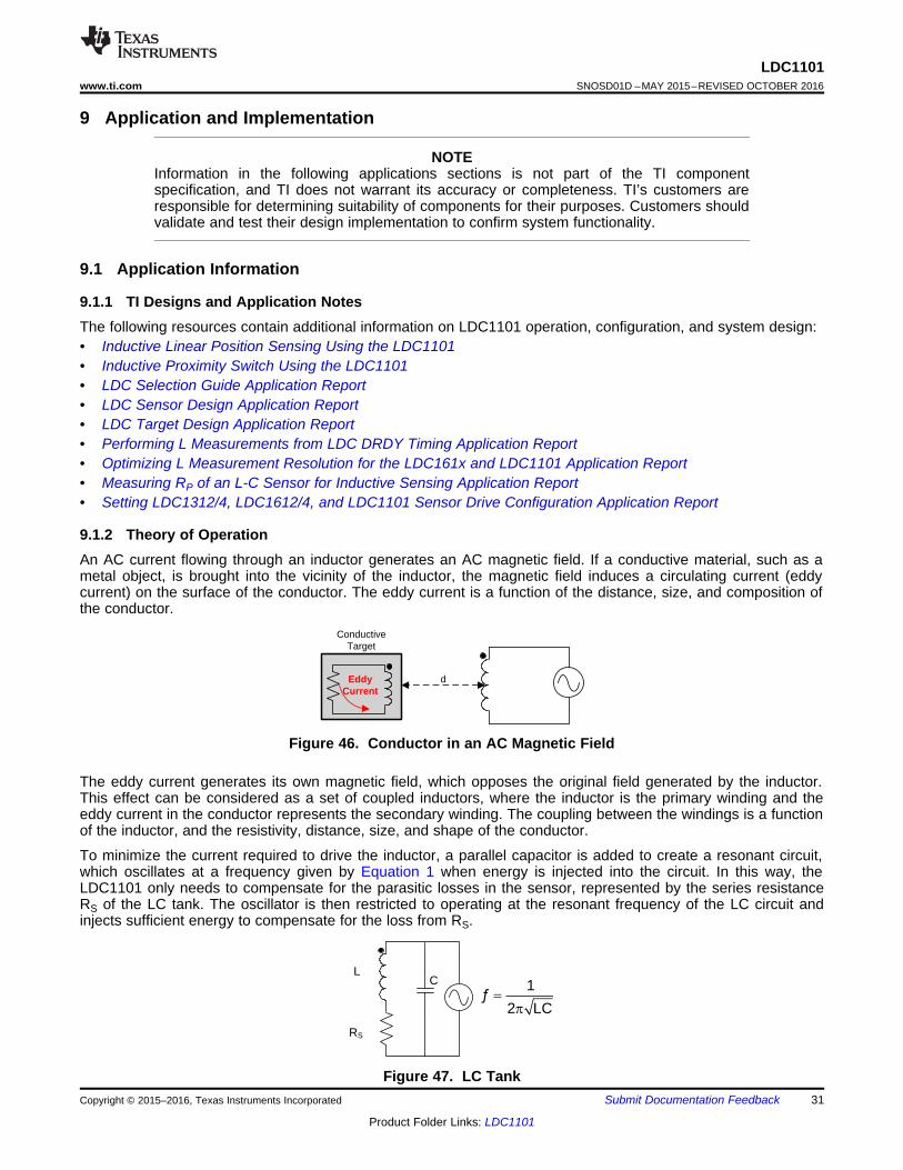
9.1.2 Theory of OperationAn AC current flowing through an inductor generates an AC magnetic field. If a conductive material, such as ametal object, is brought into the vicinity of the inductor, the magnetic field induces a circulating current (eddycurrent) on the surface of the conductor. The eddy current is a function of the distance, size, and composition ofthe conductor.
Figure 46. Conductor in an AC Magnetic Field
The eddy current generates its own magnetic field, which opposes the original field generated by the inductor.This effect can be considered as a set of coupled inductors, where the inductor is the primary winding and theeddy current in the conductor represents the secondary winding. The coupling between the windings is a functionof the inductor, and the resistivity, distance, size, and shape of the conductor.
To minimize the current required to drive the inductor, a parallel capacitor is added to create a resonant circuit,which oscillates at a frequency given by Equation 1 when energy is injected into the circuit. In this way, theLDC1101 only needs to compensate for the parasitic losses in the sensor, represented by the series resistanceRS of the LC tank. The oscillator is then restricted to operating at the resonant frequency of the LC circuit andinjects sufficient energy to compensate for the loss from RS.
Figure 47. LC Tank
Target Distance / Sensor Diameter
RP (
k:)
0 0.1 0.2 0.3 0.4 0.5 0.60
2
4
6
8
10
12
14
16
18
D010
P
s
LR
R C=
L RP C¦
1
2 LC
S
32
LDC1101SNOSD01D –MAY 2015–REVISED OCTOBER 2016 www.ti.com
Product Folder Links: LDC1101
Submit Documentation Feedback Copyright © 2015–2016, Texas Instruments Incorporated
Application Information (continued)The resistance and inductance of the secondary winding caused by the eddy current can be modeled as adistant dependent resistive and inductive component on the primary side (coil). We can then represent the circuitas an equivalent parallel circuit, as shown in Figure 48.
Figure 48. Equivalent Parallel Circuit
The value of RP can be calculated with:
where• RS is the AC series resistance at the frequency of operation.• C is the parallel capacitance• L is the inductance (2)
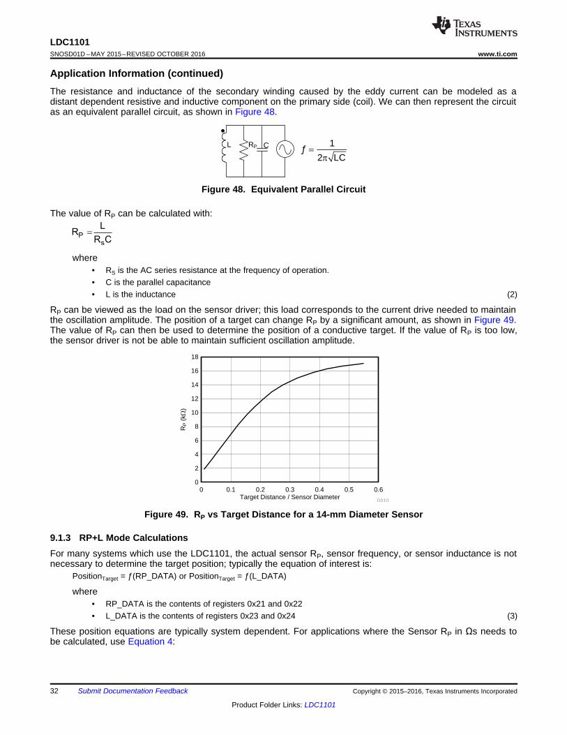
RP can be viewed as the load on the sensor driver; this load corresponds to the current drive needed to maintainthe oscillation amplitude. The position of a target can change RP by a significant amount, as shown in Figure 49.The value of RP can then be used to determine the position of a conductive target. If the value of RP is too low,the sensor driver is not be able to maintain sufficient oscillation amplitude.
Figure 49. RP vs Target Distance for a 14-mm Diameter Sensor
9.1.3 RP+L Mode CalculationsFor many systems which use the LDC1101, the actual sensor RP, sensor frequency, or sensor inductance is notnecessary to determine the target position; typically the equation of interest is:
PositionTarget = ƒ(RP_DATA) or PositionTarget = ƒ(L_DATA)
where• RP_DATA is the contents of registers 0x21 and 0x22• L_DATA is the contents of registers 0x23 and 0x24 (3)
These position equations are typically system dependent. For applications where the Sensor RP in Ωs needs tobe calculated, use Equation 4:
( )SENSOR 2
SENSOR SENSOR
1L
C 2 ƒ=
´ p
CLKINSENSOR
ƒ RESP _ TIMEƒ
3 L _DATA
´
=
´
Sensor RP (k:)
RP O
utpu
t Cod
e (D
ecim
al)
0 2.5 5 7.5 10 12.5 15 17.5 20 22.5 250
8192
16384
24576
32768
40960
49152
57344
65536
D012
MINp
16
RPR
RPDATA1
2 1
=æ ö
-ç ÷-è ø
´=
æ ö- +ç ÷
- -è ø
MAX MINp
MAX MIN16 16
RP RPR
RPDATA RPDATARP 1 RP
2 1 2 1
33
LDC1101www.ti.com SNOSD01D –MAY 2015–REVISED OCTOBER 2016
Product Folder Links: LDC1101
Submit Documentation FeedbackCopyright © 2015–2016, Texas Instruments Incorporated
Application Information (continued)
where• RPDATA is the contents of RP_DATA_MSB and RP_DATA_LSB (registers 0x21 and 0x22),• RPMIN is the value set by RP_MIN in register RP_SET (register 0x01), and• RPMAX is the value set by RP_MIN in register RP_SET (register 0x01). (4)
For example, with device settings of:• RPMIN set to 1.5 kΩ, and• RPMAX set to 12 kΩ.
If RPDATA = 0x33F1 (register 0x21 = 0xF1 and register 0x22= 0x33), which is 13297 decimal, then the sensorRP = 1.824 kΩ.
If HIGH_Q_SENSOR (Register 0x01-b[7]) is set, then the equation is simply:
(5)
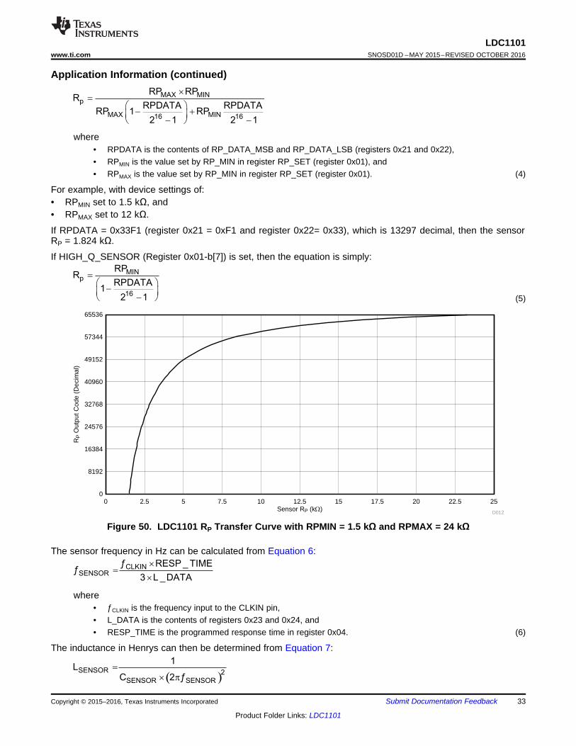
Figure 50. LDC1101 RP Transfer Curve with RPMIN = 1.5 kΩ and RPMAX = 24 kΩ
The sensor frequency in Hz can be calculated from Equation 6:
where• ƒCLKIN is the frequency input to the CLKIN pin,• L_DATA is the contents of registers 0x23 and 0x24, and• RESP_TIME is the programmed response time in register 0x04. (6)
The inductance in Henrys can then be determined from Equation 7:
Target Distance / Sensor Diameter
L (µ
H)
0 0.1 0.2 0.3 0.4 0.5 0.6 0.720
22
24
26
28
30
32
34
36
38
40
D013
34
LDC1101SNOSD01D –MAY 2015–REVISED OCTOBER 2016 www.ti.com
Product Folder Links: LDC1101
Submit Documentation Feedback Copyright © 2015–2016, Texas Instruments Incorporated
Application Information (continued)where
• CSENSOR is the fixed sensor capacitance in Farads, and• ƒSENSOR is the measured sensor frequency, as calculated in Equation 6 above. (7)
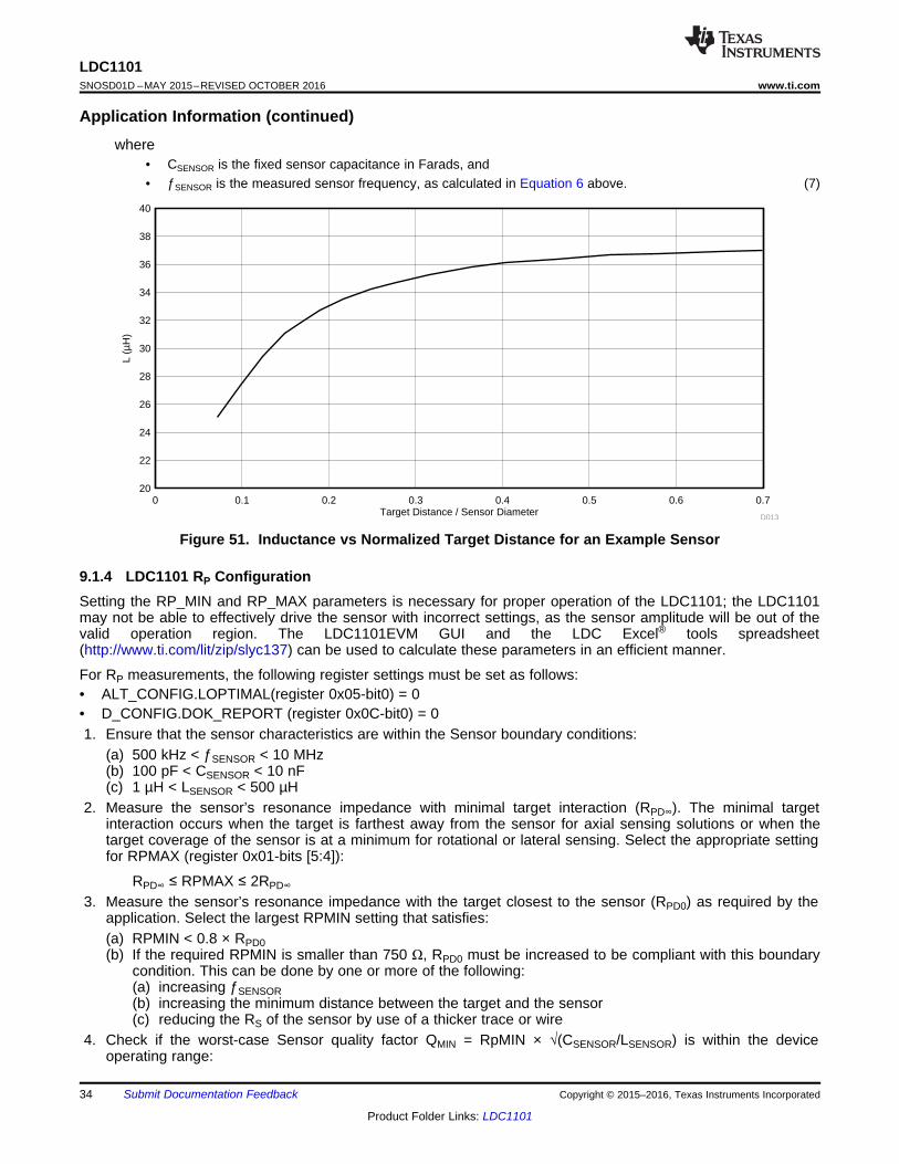
Figure 51. Inductance vs Normalized Target Distance for an Example Sensor
9.1.4 LDC1101 RP ConfigurationSetting the RP_MIN and RP_MAX parameters is necessary for proper operation of the LDC1101; the LDC1101may not be able to effectively drive the sensor with incorrect settings, as the sensor amplitude will be out of thevalid operation region. The LDC1101EVM GUI and the LDC Excel® tools spreadsheet(http://www.ti.com/lit/zip/slyc137) can be used to calculate these parameters in an efficient manner.
For RP measurements, the following register settings must be set as follows:• ALT_CONFIG.LOPTIMAL(register 0x05-bit0) = 0• D_CONFIG.DOK_REPORT (register 0x0C-bit0) = 01. Ensure that the sensor characteristics are within the Sensor boundary conditions:
(a) 500 kHz < ƒSENSOR < 10 MHz(b) 100 pF < CSENSOR < 10 nF(c) 1 µH < LSENSOR < 500 µH
2. Measure the sensor’s resonance impedance with minimal target interaction (RPD∞). The minimal targetinteraction occurs when the target is farthest away from the sensor for axial sensing solutions or when thetarget coverage of the sensor is at a minimum for rotational or lateral sensing. Select the appropriate settingfor RPMAX (register 0x01-bits [5:4]):
RPD∞ ≤ RPMAX ≤ 2RPD∞
3. Measure the sensor’s resonance impedance with the target closest to the sensor (RPD0) as required by theapplication. Select the largest RPMIN setting that satisfies:(a) RPMIN < 0.8 × RPD0(b) If the required RPMIN is smaller than 750 Ω, RPD0 must be increased to be compliant with this boundary
condition. This can be done by one or more of the following:(a) increasing ƒSENSOR(b) increasing the minimum distance between the target and the sensor(c) reducing the RS of the sensor by use of a thicker trace or wire
4. Check if the worst-case Sensor quality factor QMIN = RpMIN × √(CSENSOR/LSENSOR) is within the deviceoperating range:
1 1AMP SENSOR MIN
2R C
V ƒ-
´ =
p
35
LDC1101www.ti.com SNOSD01D –MAY 2015–REVISED OCTOBER 2016
Product Folder Links: LDC1101
Submit Documentation FeedbackCopyright © 2015–2016, Texas Instruments Incorporated
Application Information (continued)(a) 10 ≤ QMIN ≤ 400(b) If QMIN < 10, for a fixed ƒSENSOR, increase CSENSOR and decrease LSENSOR.(c) If QMIN > 400, for a fixed ƒSENSOR, decrease CSENSOR and increase LSENSOR.(d) Alternatively the user may choose to not change the current Sensor parameters, but to increase Rp_D0.
If the RP of the sensor is greater than 75 kΩ, RP measurement accuracy may be improved by settingHIGH_Q_SENSOR to 1.
9.1.5 Setting Internal Time Constant 1RP Measurements require configuration of the TC1 and TC2 registers. There are several programmablecapacitance and resistance values. Set Time Constant 1 based on minimum sensor frequency:
where• ƒSENSOR-MIN is the minimum sensor frequency encountered in the system; typically this occurs with no target
present.• VAMP is sensor amplitude of 0.6V,• R1 is the programmed setting for TC1.R1 (register 0x03-bits[4:0]), and• C1 is the programmed setting for TC1.C1 (register 0x03-bits[7:6]) (8)
The acceptable range of R1 is from 20.6 kΩ to 417.4 kΩ. If several combinations of R1 and C1 are possible, TIrecommends using the largest capacitance setting for C1 that fits the constraints of Equation 8, as this willprovide improved noise performance.
9.1.6 Setting Internal Time Constant 2Set the Time Constant 2 (register 0x03) using Equation 9:
R2 × C2 = 2 × RP_MIN × CSENSOR
where• CSENSOR is the parallel capacitance of the sensor.• RP_MIN is the LDC1101 setting determined in LDC1101 RP Configuration (for example, use 1.5 kΩ when
RP_SET.RP_MIN = b110),• R2 is the programmed setting for TC2.R2 (register 0x03-bits[5:0]), and• C2 is the programmed setting for TC2.C2 (register 0x03-bits[7:6]). (9)
The acceptable range of R2 is from 24.60 kΩ to 834.8 kΩ. If several combinations of R2 and C2 are possible, TIrecommends programming the larger capacitance setting for C2 that fits the constraints of Equation 9, as this willprovide improved noise performance.
9.1.7 MIN_FREQ and Watchdog ConfigurationThe LDC1101 includes a watchdog timer which monitors the sensor oscillation. While in active mode, if nosensor oscillation is detected, the LDC1101 sets STATUS.NO_SENSOR_OSC (register 0x20:bit7), and attemptto restart the oscillator. This restart resets any active conversion.
The watchdog waits an interval of time based on the setting of DIG_CONF.MIN_FREQ (register 0x04:bits[7:4]).The MIN_FREQ setting is also used to configure the start-up of oscillation on the sensor. Select theDIG_CONF.MIN_FREQ (register 0x04-bits[7:4]) setting closest to the minimum sensor frequency; this setting isused for internal watchdog timing. If the watchdog determines the sensor has stopped oscillating, it reports thesensor has stopped oscillating in STATUS. NO_SENSOR_OSC (register 0x20-bit7). If theDIG_CONF.MIN_FREQ is set too low, then the LDC1101 takes a longer time interval to report that the sensoroscillation has stopped.
If the DIG_CONF.MIN_FREQ is set too high, then the watchdog may incorrectly report that the sensor hasstopped oscillating and attempt to restart the sensor oscillation.
( )1 8
SENSOR 24
2 1 6 MHz 1193046 255 2ƒ
2
´ + ´=
( )SENSOR 2
SENSOR SENSOR
1L
C 2 ƒ=
´ p
( )SENSORDIV 8CLKIN
SENSOR 24
2 ƒ LHRDATA LHROFFSET 2ƒ
2
´ + ´=
( )SENSOR
Response TimeConversion Time s
3 ƒ=
´
36
LDC1101SNOSD01D –MAY 2015–REVISED OCTOBER 2016 www.ti.com
Product Folder Links: LDC1101
Submit Documentation Feedback Copyright © 2015–2016, Texas Instruments Incorporated
Application Information (continued)When the watchdog determines that the sensor has stopped oscillating, the LHR conversion results will contain0xFFFFFF.
9.1.8 RP+L Sample Rate Configuration With RESP_TIMEThe RP+L sample rate can be adjusted by setting by DIG_CONF.RESP_TIME (register 0x04:bits[2:0]). TheResponse time can be configured from 192 to 6144 cycles of the sensor frequency. Higher values of Responsetime have a slower sample rate, but produce a higher resolution conversion.
(10)
For applications which require only RP measurements, it is not necessary to apply a reference frequency on theCLKIN pin. If there is to be no signal input on CLKIN, is recommended to tie CLKIN to ground in this situation.The L and LHR measurements will return 0.
9.1.9 High Resolution Inductance Calculation (LHR mode)For many systems which use the LDC1101, the actual sensor frequency or sensor inductance is not necessaryto determine the target position. Should the sensor frequency in Hz need to be determined, use Equation 11:
where• LHRDATA is the contents of registers 0x38, 0x39, and 0x3A,• LHROFFSET is the programmed contents of registers 0x32 and 0x33,• SENSOR_DIV is the contents of LHR_CONFIG.SENSOR_DIV (register 0x34-bit[1:0]), and• ƒCLKIN is the frequency input to the CLKIN pin: ensure that it is within the specified limits of 1 MHz to 16
MHz. (11)
Note that LHR_DATA=0x0000000 indicates a fault condition or that the LDC1101 has never completed an LHRconversion.
The inductance in Henrys can then be determined from the sensor frequency with Equation 12:
where• CSENSOR is the fixed sensor capacitance, and• ƒSENSOR is the measured sensor frequency, as calculated above. (12)
Example with the device set to:• LHR_OFFSET = 0x00FF (register 0x32 = 0xFF, and 0x33 = 0x00)• ƒCLKIN = 16 MHz• SENSOR_DIV = b’01 (divide by 2)
and the conversion result is:
LHR_DATA = 0x123456 (register 0x38 = 0x56, register 0x39 = 0x34,register 0x3A = 0x12)
Then entering LHR_DATA = 0x123456 = 1193046 (decimal) into Equation 11:
(13)
Results in ƒSENSOR = 2.400066 MHz.
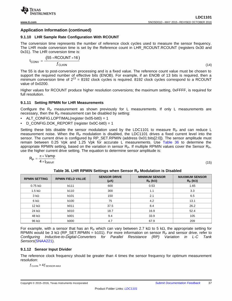
PDRIVE
VampR
4 I
p ´
=
´
( )CONV
CLKIN
55 RCOUNT 1 6t
ƒ
+ ´=
37
LDC1101www.ti.com SNOSD01D –MAY 2015–REVISED OCTOBER 2016
Product Folder Links: LDC1101
Submit Documentation FeedbackCopyright © 2015–2016, Texas Instruments Incorporated
Application Information (continued)9.1.10 LHR Sample Rate Configuration With RCOUNTThe conversion time represents the number of reference clock cycles used to measure the sensor frequency.The LHR mode conversion time is set by the Reference count in LHR_RCOUNT.RCOUNT (registers 0x30 and0x31). The LHR conversion time is:
(14)
The 55 is due to post-conversion processing and is a fixed value. The reference count value must be chosen tosupport the required number of effective bits (ENOB). For example, if an ENOB of 13 bits is required, then aminimum conversion time of 213 = 8192 clock cycles is required. 8192 clock cycles correspond to a RCOUNTvalue of 0x0200.
Higher values for RCOUNT produce higher resolution conversions; the maximum setting, 0xFFFF, is required forfull resolution.
9.1.11 Setting RPMIN for LHR MeasurementsConfigure the RP measurement as shown previously for L measurements. If only L measurements arenecessary, then the RP measurement can be disabled by setting:• ALT_CONFIG.LOPTIMAL(register 0x05-bit0) = 1• D_CONFIG.DOK_REPORT (register 0x0C-bit0) = 1
Setting these bits disable the sensor modulation used by the LDC1101 to measure RP and can reduce Lmeasurement noise. When the RP modulation is disabled, the LDC1101 drives a fixed current level into thesensor. The current drive is configured by RP_SET.RPMIN (address 0x01:bits[2:0]). The sensor amplitude mustremain between 0.25 Vpk and 1.25 Vpk for accurate L measurements. Use Table 36 to determine theappropriate RPMIN setting, based on the variation in sensor RP. If multiple RPMIN values cover the Sensor RP,use the higher current drive setting. The equation to determine sensor amplitude is:
(15)
Table 36. LHR RPMIN Settings when Sensor RP Modulation is Disabled
RPMIN SETTING RPMIN FIELD VALUE SENSOR DRIVE(μA)
MINIMUM SENSORRP (kΩ)
MAXIMUM SENSORRP (kΩ)
0.75 kΩ b111 600 0.53 1.651.5 kΩ b110 300 1.1 3.33 kΩ b101 150 2.1 6.56 kΩ b100 75 4.2 13.112 kΩ b011 37.5 8.4 26.224 kΩ b010 18.7 16.9 52.448 kΩ b001 9.4 33.9 10596 kΩ b000 4.7 67.9 209
For example, with a sensor that has an RP which can vary between 2.7 kΩ to 5 kΩ, the appropriate setting forRPMIN would be 3 kΩ (RP_SET.RPMIN = b101). For more information on sensor RP and sensor drive, refer toConfiguring Inductive-to-Digital-Converters for Parallel Resistance (RP) Variation in L-C TankSensors(SNAA221).
9.1.12 Sensor Input DividerThe reference clock frequency should be greater than 4 times the sensor frequency for optimum measurementresolution:
ƒCLKIN > 4ƒSENSOR-MAX
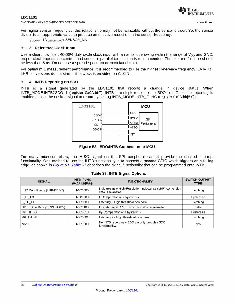
LDC1101
SCLK
CSB
SDO
SDI
MCU
SPIPeripheral
SCLK
CSB
MISOMOSI
INT
38
LDC1101SNOSD01D –MAY 2015–REVISED OCTOBER 2016 www.ti.com
Product Folder Links: LDC1101
Submit Documentation Feedback Copyright © 2015–2016, Texas Instruments Incorporated
For higher sensor frequencies, this relationship may not be realizable without the sensor divider. Set the sensordivider to an appropriate value to produce an effective reduction in the sensor frequency:
ƒCLKIN > 4ƒSENSOR-MAX ÷ SENSOR_DIV
9.1.13 Reference Clock InputUse a clean, low jitter, 40-60% duty cycle clock input with an amplitude swing within the range of VDD and GND;proper clock impedance control, and series or parallel termination is recommended. The rise and fall time shouldbe less than 5 ns. Do not use a spread-spectrum or modulated clock.
For optimum L measurement performance, it is recommended to use the highest reference frequency (16 MHz).LHR conversions do not start until a clock is provided on CLKIN.
9.1.14 INTB Reporting on SDOINTB is a signal generated by the LDC1101 that reports a change in device status. WhenINTB_MODE.INTB2SDO=1 (register 0x0A:bit7), INTB is multiplexed onto the SDO pin. Once the reporting isenabled, select the desired signal to report by setting INTB_MODE.INTB_FUNC (register 0x0A:bit[5:0]).
Figure 52. SDO/INTB Connection to MCU
For many microcontrollers, the MISO signal on the SPI peripheral cannot provide the desired interruptfunctionality. One method to use the INTB functionality is to connect a second GPIO which triggers on a fallingedge, as shown in Figure 51. Table 37 describes the signal functionality that can be programmed onto INTB.
Table 37. INTB Signal Options
SIGNAL INTB_FUNC(0x0A:bit[5:0]) FUNCTIONALITY SWITCH OUTPUT
TYPE
LHR Data Ready (LHR-DRDY) b10’0000 Indicates new High-Resolution Inductance (LHR) conversiondata is available. Latching
L_HI_LO b01’0000 L Comparator with hysteresis HysteresisL_TH_HI b00’1000 Latching L High threshold compare LatchingRP+L Data Ready (RPL-DRDY) b00’0100 Indicates new RP+L conversion data is available. PulseRP_HI_LO b00’0010 RP Comparator with hysteresis HysteresisRP_TH_HI b00’0001 Latching RP High threshold compare Latching
None b00’0000 No INTB reporting – SDO pin only provides SDOfunctionality. N/A
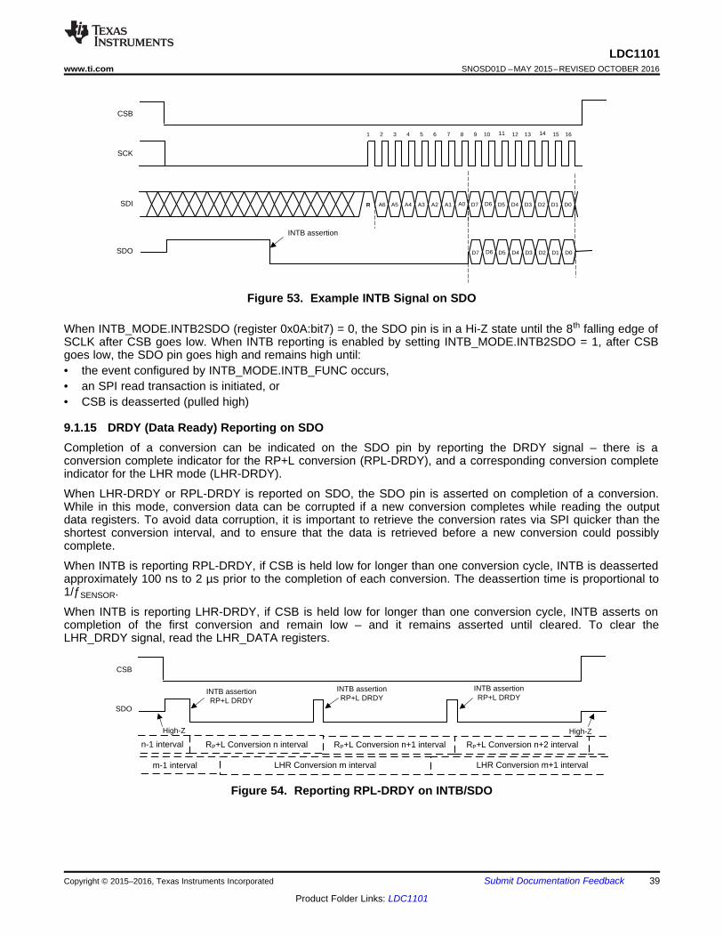
CSB
SDO
INTB assertionRP+L DRDY
High-Z High-Z
INTB assertionRP+L DRDY
INTB assertionRP+L DRDY
RP+L Conversion n+1 intervaln-1 interval
m-1 interval LHR Conversion m+1 interval
RP+L Conversion n interval RP+L Conversion n+2 interval
LHR Conversion m interval
A6 A5 A4 A3 A2 A1 A0 D7 D6 D5 D4 D3 D2 D1
CSB
SCK
1 2 3 4 5 6 7 8 9 10 11 12 13 14 15 16
SDI
D7 D6 D5 D4 D3 D2 D1SDO
R
D0
D0
INTB assertion
39
LDC1101www.ti.com SNOSD01D –MAY 2015–REVISED OCTOBER 2016
Product Folder Links: LDC1101
Submit Documentation FeedbackCopyright © 2015–2016, Texas Instruments Incorporated
Figure 53. Example INTB Signal on SDO
When INTB_MODE.INTB2SDO (register 0x0A:bit7) = 0, the SDO pin is in a Hi-Z state until the 8th falling edge ofSCLK after CSB goes low. When INTB reporting is enabled by setting INTB_MODE.INTB2SDO = 1, after CSBgoes low, the SDO pin goes high and remains high until:• the event configured by INTB_MODE.INTB_FUNC occurs,• an SPI read transaction is initiated, or• CSB is deasserted (pulled high)
9.1.15 DRDY (Data Ready) Reporting on SDOCompletion of a conversion can be indicated on the SDO pin by reporting the DRDY signal – there is aconversion complete indicator for the RP+L conversion (RPL-DRDY), and a corresponding conversion completeindicator for the LHR mode (LHR-DRDY).
When LHR-DRDY or RPL-DRDY is reported on SDO, the SDO pin is asserted on completion of a conversion.While in this mode, conversion data can be corrupted if a new conversion completes while reading the outputdata registers. To avoid data corruption, it is important to retrieve the conversion rates via SPI quicker than theshortest conversion interval, and to ensure that the data is retrieved before a new conversion could possiblycomplete.
When INTB is reporting RPL-DRDY, if CSB is held low for longer than one conversion cycle, INTB is deassertedapproximately 100 ns to 2 µs prior to the completion of each conversion. The deassertion time is proportional to1/ƒSENSOR.
When INTB is reporting LHR-DRDY, if CSB is held low for longer than one conversion cycle, INTB asserts oncompletion of the first conversion and remain low – and it remains asserted until cleared. To clear theLHR_DRDY signal, read the LHR_DATA registers.
Figure 54. Reporting RPL-DRDY on INTB/SDO
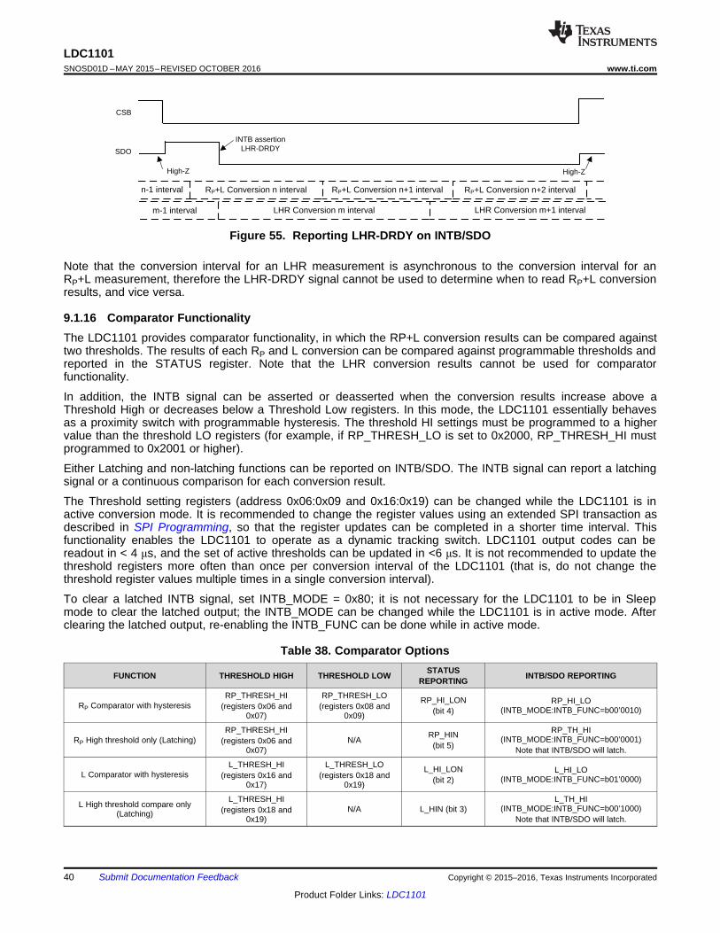
CSB
SDO
INTB assertionLHR-DRDY
High-Z High-Z
RP+L Conversion n+1 intervaln-1 interval
m-1 interval LHR Conversion m+1 interval
RP+L Conversion n interval RP+L Conversion n+2 interval
LHR Conversion m interval
40
LDC1101SNOSD01D –MAY 2015–REVISED OCTOBER 2016 www.ti.com
Product Folder Links: LDC1101
Submit Documentation Feedback Copyright © 2015–2016, Texas Instruments Incorporated
Figure 55. Reporting LHR-DRDY on INTB/SDO
Note that the conversion interval for an LHR measurement is asynchronous to the conversion interval for anRP+L measurement, therefore the LHR-DRDY signal cannot be used to determine when to read RP+L conversionresults, and vice versa.
9.1.16 Comparator FunctionalityThe LDC1101 provides comparator functionality, in which the RP+L conversion results can be compared againsttwo thresholds. The results of each RP and L conversion can be compared against programmable thresholds andreported in the STATUS register. Note that the LHR conversion results cannot be used for comparatorfunctionality.
In addition, the INTB signal can be asserted or deasserted when the conversion results increase above aThreshold High or decreases below a Threshold Low registers. In this mode, the LDC1101 essentially behavesas a proximity switch with programmable hysteresis. The threshold HI settings must be programmed to a highervalue than the threshold LO registers (for example, if RP_THRESH_LO is set to 0x2000, RP_THRESH_HI mustprogrammed to 0x2001 or higher).
Either Latching and non-latching functions can be reported on INTB/SDO. The INTB signal can report a latchingsignal or a continuous comparison for each conversion result.
The Threshold setting registers (address 0x06:0x09 and 0x16:0x19) can be changed while the LDC1101 is inactive conversion mode. It is recommended to change the register values using an extended SPI transaction asdescribed in SPI Programming, so that the register updates can be completed in a shorter time interval. Thisfunctionality enables the LDC1101 to operate as a dynamic tracking switch. LDC1101 output codes can bereadout in < 4 μs, and the set of active thresholds can be updated in <6 μs. It is not recommended to update thethreshold registers more often than once per conversion interval of the LDC1101 (that is, do not change thethreshold register values multiple times in a single conversion interval).
To clear a latched INTB signal, set INTB_MODE = 0x80; it is not necessary for the LDC1101 to be in Sleepmode to clear the latched output; the INTB_MODE can be changed while the LDC1101 is in active mode. Afterclearing the latched output, re-enabling the INTB_FUNC can be done while in active mode.
Table 38. Comparator Options
FUNCTION THRESHOLD HIGH THRESHOLD LOW STATUSREPORTING INTB/SDO REPORTING
RP Comparator with hysteresisRP_THRESH_HI
(registers 0x06 and0x07)
RP_THRESH_LO(registers 0x08 and
0x09)
RP_HI_LON(bit 4)
RP_HI_LO(INTB_MODE:INTB_FUNC=b00’0010)
RP High threshold only (Latching)RP_THRESH_HI
(registers 0x06 and0x07)
N/A RP_HIN(bit 5)
RP_TH_HI(INTB_MODE:INTB_FUNC=b00’0001)
Note that INTB/SDO will latch.
L Comparator with hysteresisL_THRESH_HI
(registers 0x16 and0x17)
L_THRESH_LO(registers 0x18 and
0x19)
L_HI_LON(bit 2)
L_HI_LO(INTB_MODE:INTB_FUNC=b01’0000)
L High threshold compare only(Latching)
L_THRESH_HI(registers 0x18 and
0x19)N/A L_HIN (bit 3)
L_TH_HI(INTB_MODE:INTB_FUNC=b00’1000)
Note that INTB/SDO will latch.
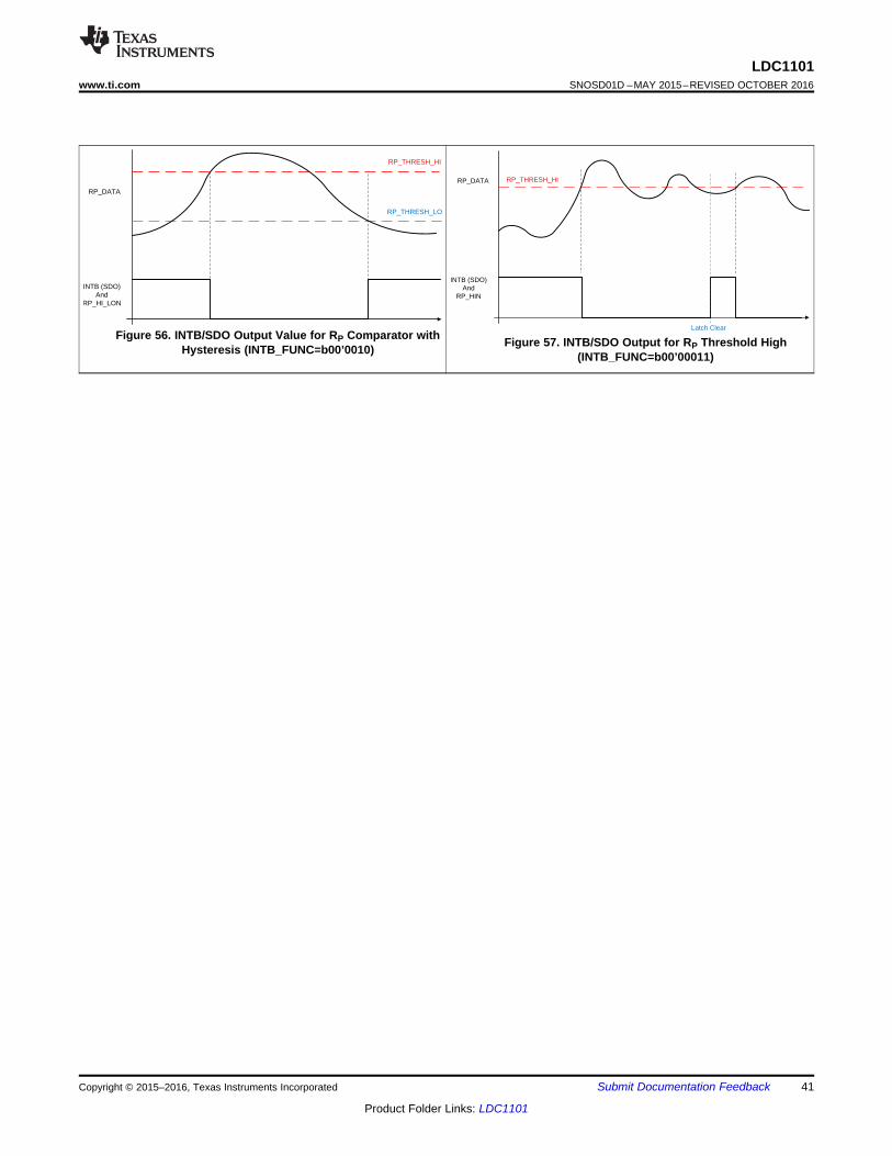
INTB (SDO)And
RP_HIN
RP_THRESH_HIRP_DATA
Latch Clear
INTB (SDO)And
RP_HI_LON
RP_THRESH_HI
RP_THRESH_LO
RP_DATA
41
LDC1101www.ti.com SNOSD01D –MAY 2015–REVISED OCTOBER 2016
Product Folder Links: LDC1101
Submit Documentation FeedbackCopyright © 2015–2016, Texas Instruments Incorporated
space
Figure 56. INTB/SDO Output Value for RP Comparator withHysteresis (INTB_FUNC=b00’0010) Figure 57. INTB/SDO Output for RP Threshold High
(INTB_FUNC=b00’00011)
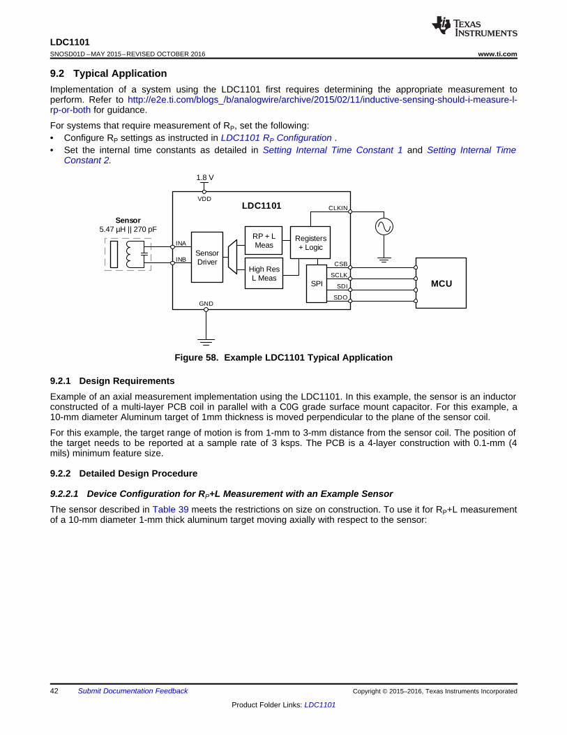
RP + L MeasINA
INB
LDC1101VDD
Registers + Logic
GND
SPI
CLKIN
SCLK
CSB
SDO
SDI
High Res L Meas
Sensor Driver
MCU
1.8 V
Sensor5.47 µH || 270 pF
42
LDC1101SNOSD01D –MAY 2015–REVISED OCTOBER 2016 www.ti.com
Product Folder Links: LDC1101
Submit Documentation Feedback Copyright © 2015–2016, Texas Instruments Incorporated
9.2 Typical ApplicationImplementation of a system using the LDC1101 first requires determining the appropriate measurement toperform. Refer to http://e2e.ti.com/blogs_/b/analogwire/archive/2015/02/11/inductive-sensing-should-i-measure-l-rp-or-both for guidance.
For systems that require measurement of RP, set the following:• Configure RP settings as instructed in LDC1101 RP Configuration .• Set the internal time constants as detailed in Setting Internal Time Constant 1 and Setting Internal Time
Constant 2.
Figure 58. Example LDC1101 Typical Application
9.2.1 Design RequirementsExample of an axial measurement implementation using the LDC1101. In this example, the sensor is an inductorconstructed of a multi-layer PCB coil in parallel with a C0G grade surface mount capacitor. For this example, a10-mm diameter Aluminum target of 1mm thickness is moved perpendicular to the plane of the sensor coil.
For this example, the target range of motion is from 1-mm to 3-mm distance from the sensor coil. The position ofthe target needs to be reported at a sample rate of 3 ksps. The PCB is a 4-layer construction with 0.1-mm (4mils) minimum feature size.
9.2.2 Detailed Design Procedure
9.2.2.1 Device Configuration for RP+L Measurement with an Example SensorThe sensor described in Table 39 meets the restrictions on size on construction. To use it for RP+L measurementof a 10-mm diameter 1-mm thick aluminum target moving axially with respect to the sensor:
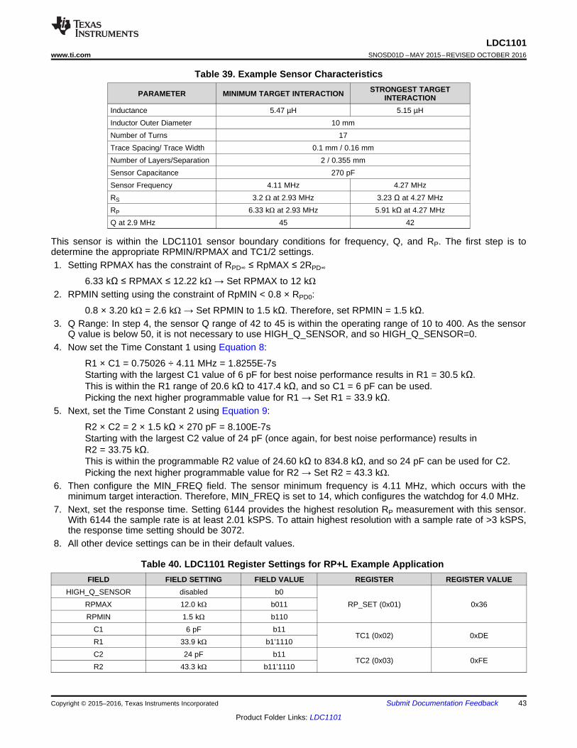
43
LDC1101www.ti.com SNOSD01D –MAY 2015–REVISED OCTOBER 2016
Product Folder Links: LDC1101
Submit Documentation FeedbackCopyright © 2015–2016, Texas Instruments Incorporated
Table 39. Example Sensor Characteristics
PARAMETER MINIMUM TARGET INTERACTION STRONGEST TARGETINTERACTION
Inductance 5.47 µH 5.15 µHInductor Outer Diameter 10 mmNumber of Turns 17Trace Spacing/ Trace Width 0.1 mm / 0.16 mmNumber of Layers/Separation 2 / 0.355 mmSensor Capacitance 270 pFSensor Frequency 4.11 MHz 4.27 MHzRS 3.2 Ω at 2.93 MHz 3.23 Ω at 4.27 MHzRP 6.33 kΩ at 2.93 MHz 5.91 kΩ at 4.27 MHzQ at 2.9 MHz 45 42
This sensor is within the LDC1101 sensor boundary conditions for frequency, Q, and RP. The first step is todetermine the appropriate RPMIN/RPMAX and TC1/2 settings.1. Setting RPMAX has the constraint of RPD∞ ≤ RpMAX ≤ 2RPD∞
6.33 kΩ ≤ RPMAX ≤ 12.22 kΩ → Set RPMAX to 12 kΩ2. RPMIN setting using the constraint of RpMIN < 0.8 × RPD0:
0.8 × 3.20 kΩ = 2.6 kΩ → Set RPMIN to 1.5 kΩ. Therefore, set RPMIN = 1.5 kΩ.3. Q Range: In step 4, the sensor Q range of 42 to 45 is within the operating range of 10 to 400. As the sensor
Q value is below 50, it is not necessary to use HIGH_Q_SENSOR, and so HIGH_Q_SENSOR=0.4. Now set the Time Constant 1 using Equation 8:
R1 × C1 = 0.75026 ÷ 4.11 MHz = 1.8255E-7sStarting with the largest C1 value of 6 pF for best noise performance results in R1 = 30.5 kΩ.This is within the R1 range of 20.6 kΩ to 417.4 kΩ, and so C1 = 6 pF can be used.Picking the next higher programmable value for R1 → Set R1 = 33.9 kΩ.
5. Next, set the Time Constant 2 using Equation 9:
R2 × C2 = 2 × 1.5 kΩ × 270 pF = 8.100E-7sStarting with the largest C2 value of 24 pF (once again, for best noise performance) results inR2 = 33.75 kΩ.This is within the programmable R2 value of 24.60 kΩ to 834.8 kΩ, and so 24 pF can be used for C2.Picking the next higher programmable value for R2 → Set R2 = 43.3 kΩ.
6. Then configure the MIN_FREQ field. The sensor minimum frequency is 4.11 MHz, which occurs with theminimum target interaction. Therefore, MIN_FREQ is set to 14, which configures the watchdog for 4.0 MHz.
7. Next, set the response time. Setting 6144 provides the highest resolution RP measurement with this sensor.With 6144 the sample rate is at least 2.01 kSPS. To attain highest resolution with a sample rate of >3 kSPS,the response time setting should be 3072.
8. All other device settings can be in their default values.
Table 40. LDC1101 Register Settings for RP+L Example ApplicationFIELD FIELD SETTING FIELD VALUE REGISTER REGISTER VALUE
HIGH_Q_SENSOR disabled b0RP_SET (0x01) 0x36RPMAX 12.0 kΩ b011
RPMIN 1.5 kΩ b110C1 6 pF b11
TC1 (0x02) 0xDER1 33.9 kΩ b1’1110C2 24 pF b11
TC2 (0x03) 0xFER2 43.3 kΩ b11’1110
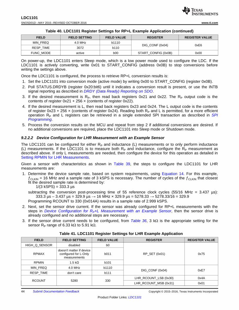
44
LDC1101SNOSD01D –MAY 2015–REVISED OCTOBER 2016 www.ti.com
Product Folder Links: LDC1101
Submit Documentation Feedback Copyright © 2015–2016, Texas Instruments Incorporated
Table 40. LDC1101 Register Settings for RP+L Example Application (continued)FIELD FIELD SETTING FIELD VALUE REGISTER REGISTER VALUE
MIN_FREQ 4.0 MHz b1110DIG_CONF (0x04) 0xE6
RESP_TIME 3072 b110FUNC_MODE active b00 START_CONFIG (0x0B) 0x00
On power-up, the LDC1101 enters Sleep mode, which is a low power mode used to configure the LDC. If theLDC1101 is actively converting, write 0x01 to START_CONFIG (address 0x0B) to stop conversions beforewriting the settings above.
Once the LDC1101 is configured, the process to retrieve RP+L conversion results is:1. Set the LDC1101 into conversion mode (active mode) by writing 0x00 to START_CONFIG (register 0x0B).2. Poll STATUS.DRDYB (register 0x20:bit6) until it indicates a conversion result is present, or use the INTB
signal reporting as described in DRDY (Data Ready) Reporting on SDO.3. If the desired measurement is RP, then read back registers 0x21 and 0x22. The RP output code is the
contents of register 0x21 + 256 × (contents of register 0x22).4. If the desired measurement is L, then read back registers 0x23 and 0x24. The L output code is the contents
of register 0x23 + 256 × (contents of register 0x24). Reading both RP and L is permitted, for a more efficientoperation RP and L registers can be retrieved in a single extended SPI transaction as described in SPIProgramming.
5. Process the conversion results on the MCU and repeat from step 2 if additional conversions are desired. Ifno additional conversions are required, place the LDC1101 into Sleep mode or Shutdown mode.
9.2.2.2 Device Configuration for LHR Measurement with an Example SensorThe LDC1101 can be configured for either RP and inductance (L) measurements or to only perform inductance(L) measurements. If the LDC1101 is to measure both RP and inductance, configure the RP measurement asdescribed above. If only L measurements are needed, then configure the device for this operation as detailed inSetting RPMIN for LHR Measurements.
Given a sensor with characteristics as shown in Table 39, the steps to configure the LDC1101 for LHRmeasurements are:1. Determine the device sample rate, based on system requirements, using Equation 14. For this example,
ƒCLKIN = 16 MHz and a sample rate of 3 kSPS is necessary. The number of cycles of the ƒCLKIN that closestfit the desired sample rate is determined by:mm 1/(3 kSPS) = 333.3 µssubtracting the conversion post-processing time of 55 reference clock cycles (55/16 MHz = 3.437 µs):mm 333.3 µs – 3.437 µs = 329.9 µs → 16 MHz × 329.9 µs = 5278.33 → 5278.33/16 = 329.9Programming RCOUNT to 330 (0x014A) results in a sample rate of 2.999 kSPS.
2. Next, set the sensor drive current. If the sensor was already configured for RP+L measurements with thesteps in Device Configuration for RP+L Measurement with an Example Sensor, then the sensor drive isalready configured and no additional steps are necessary.
3. If the sensor drive current needs to be configured, from Table 36, 3 kΩ is the appropriate setting for thesensor RP range of 6.33 kΩ to 5.91 kΩ.
Table 41. LDC1101 Register Settings for LHR Example ApplicationFIELD FIELD SETTING FIELD VALUE REGISTER REGISTER VALUE
HIGH_Q_SENSOR disabled b0
RP_SET (0x01) 0x75RPMAXdoesn’t matter if deviceconfigured for L-Only
measurementsb011
RPMIN 1.5 kΩ b101MIN_FREQ 4.0 MHz b1110
DIG_CONF (0x04) 0xE7RESP_TIME don’t care b111
RCOUNT 5280 330LHR_RCOUNT_LSB (0x30) 0x4ALHR_RCOUNT_MSB (0x31) 0x01
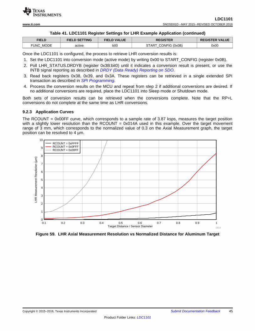
Target Distance / Sensor Diameter
LHR
Mea
sure
men
t Res
olut
ion
(µm
)
0.1 0.2 0.3 0.4 0.5 0.6 0.7 0.8 0.9 10
1
2
3
4
5
6
7
8
9
10
D014
RCOUNT = 0xFFFFRCOUNT = 0x0FFFRCOUNT = 0x00FF
45
LDC1101www.ti.com SNOSD01D –MAY 2015–REVISED OCTOBER 2016
Product Folder Links: LDC1101
Submit Documentation FeedbackCopyright © 2015–2016, Texas Instruments Incorporated
Table 41. LDC1101 Register Settings for LHR Example Application (continued)FIELD FIELD SETTING FIELD VALUE REGISTER REGISTER VALUE
FUNC_MODE active b00 START_CONFIG (0x0B) 0x00
Once the LDC1101 is configured, the process to retrieve LHR conversion results is:1. Set the LDC1101 into conversion mode (active mode) by writing 0x00 to START_CONFIG (register 0x0B).2. Poll LHR_STATUS.DRDYB (register 0x3B:bit0) until it indicates a conversion result is present, or use the
INTB signal reporting as described in DRDY (Data Ready) Reporting on SDO.3. Read back registers 0x38, 0x39, and 0x3A. These registers can be retrieved in a single extended SPI
transaction as described in SPI Programming.4. Process the conversion results on the MCU and repeat from step 2 if additional conversions are desired. If
no additional conversions are required, place the LDC1101 into Sleep mode or Shutdown mode.
Both sets of conversion results can be retrieved when the conversions complete. Note that the RP+Lconversions do not complete at the same time as LHR conversions.
9.2.3 Application CurvesThe RCOUNT = 0x00FF curve, which corresponds to a sample rate of 3.87 ksps, measures the target positionwith a slightly lower resolution than the RCOUNT = 0x014A used in this example. Over the target movementrange of 3 mm, which corresponds to the normalized value of 0.3 on the Axial Measurement graph, the targetposition can be resolved to 4 µm.
Figure 59. LHR Axial Measurement Resolution vs Normalized Distance for Aluminum Target
Target Distance / Sensor Diameter
LHR
Out
put C
ode
(DE
C)
0 0.1 0.2 0.3 0.4 0.5 0.6 0.7 0.8 0.9 14000000
4500000
5000000
5500000
6000000
6500000
7000000
7500000
D015
46
LDC1101SNOSD01D –MAY 2015–REVISED OCTOBER 2016 www.ti.com
Product Folder Links: LDC1101
Submit Documentation Feedback Copyright © 2015–2016, Texas Instruments Incorporated
Figure 60. LHR Output Code vs Normalized Distance for Aluminum Target

47
LDC1101www.ti.com SNOSD01D –MAY 2015–REVISED OCTOBER 2016
Product Folder Links: LDC1101
Submit Documentation FeedbackCopyright © 2015–2016, Texas Instruments Incorporated
10 Power Supply RecommendationsA parallel set of 1-µF and 0.1-µF capacitors must be used to bypass VDD, although it may be necessary toinclude a larger capacitor with systems which have a larger amount of supply variation. The smallest valuecapacitor should be placed as close to the VDD pin as possible. A ground plane is recommended to connectboth the ground and the die attach pad (DAP).
CLDO capacitor must be nonpolarized and have an equivalent series resistance (ESR) less than 1 Ω, with a SRFof at least 24 MHz.
11 Layout
11.1 Layout GuidelinesThe LDC1101 requires minimal external components for effective operation. Following good layout techniquesproviding good grounding and clean supplies are critical for optimum operation. Due to the small physical size ofthe LDC1101, use of surface mount 0402 or smaller components can ease routing.
11.1.1 Ground and Power PlanesGround and power planes are helpful for maintaining a clean supply to the LDC1101. In the layout shown inFigure 61, a top-layer ground fill is also used for improved grounding.
11.1.2 CLKIN RoutingThe CLKIN pin routing must maintain consistent impedance; typically this is 50 Ω, but can be adjusted based onboard geometries. If a parallel termination resistor is used, it must be placed as close to the CLKIN pin aspossible. Minimize layer changes and routing through vias for the CLKIN signal. Maintain an uninterruptedground plane under the trace.
11.1.3 Capacitor PlacementThe capacitor CLDO must be placed as close to the CLDO pin as possible.
Place the bypass capacitors as close to the VDD pin as possible, with the smaller valued capacitor placed closer.
11.1.4 Sensor ConnectionsThe sensor capacitor must be as close to the sensor inductor as possible. The INA and INB traces must berouted in parallel and as close to each other as possible to minimize coupling of noise. If cable is to be used,then INA and INB should be a twisted pair or in coaxial cable. The distance between the INA/INB pins and thesensor affects the maximum possible sensor frequency. For some applications, it may be helpful to place small-value capacitor (for example, 10 pF) from INA to ground and INB to ground; these capacitors should be locatedclose to the INA and INB pins.
Refer to Application Note LDC Sensor Design (SNOA930) for additional information on sensor design.

48
LDC1101SNOSD01D –MAY 2015–REVISED OCTOBER 2016 www.ti.com
Product Folder Links: LDC1101
Submit Documentation Feedback Copyright © 2015–2016, Texas Instruments Incorporated
11.2 Layout Example
Figure 61. Layout Recommendations
49
LDC1101www.ti.com SNOSD01D –MAY 2015–REVISED OCTOBER 2016
Product Folder Links: LDC1101
Submit Documentation FeedbackCopyright © 2015–2016, Texas Instruments Incorporated
12 Device and Documentation Support
12.1 Device Support
12.1.1 Development SupportFor on-line LDC system design tools, see Texas Instruments' Webench® Tool.
The LDC Calculator tools provides a collection of calculation tools which run under MS Excel® useful for LDCsystem development.
12.2 Documentation Support
12.2.1 Related DocumentationFor detailed information on LDC sensor design, refer to the application report LDC Sensor Design.
For detailed information on lateral position sensing with an LDC, in which a target is moved at a constant heightfrom a sensor and the offset is to be measured, refer to LDC1612/LDC1614 Linear Position Sensing. TheLDC1101 LHR mode is functionally equivalent to a single channel LDC1612/LDC1614.
For information on temperature compensation, refer to LDC1000 Temperature Compensation.
The following resources contain additional information on LDC1101 operation, configuration, and system design:• Inductive Linear Position Sensing Using the LDC1101• Inductive Proximity Switch Using the LDC1101• LDC Selection Guide Application Report• LDC Sensor Design Application Report• LDC Target Design Application Report• Performing L Measurements from LDC DRDY Timing Application Report• Optimizing L Measurement Resolution for the LDC161x and LDC1101 Application Report• Measuring RP of an L-C Sensor for Inductive Sensing Application Report• Setting LDC1312/4, LDC1612/4, and LDC1101 Sensor Drive Configuration Application Report
12.3 Community ResourcesThe following links connect to TI community resources. Linked contents are provided "AS IS" by the respectivecontributors. They do not constitute TI specifications and do not necessarily reflect TI's views; see TI's Terms ofUse.
TI E2E™ Online Community TI's Engineer-to-Engineer (E2E) Community. Created to foster collaborationamong engineers. At e2e.ti.com, you can ask questions, share knowledge, explore ideas and helpsolve problems with fellow engineers.
Design Support TI's Design Support Quickly find helpful E2E forums along with design support tools andcontact information for technical support.
12.4 TrademarksE2E is a trademark of Texas Instruments.Webench is a registered trademark of Texas Instruments.Excel is a registered trademark of Microsoft Corporation.SPI is a trademark of Motorola.All other trademarks are the property of their respective owners.
12.5 Electrostatic Discharge CautionThese devices have limited built-in ESD protection. The leads should be shorted together or the device placed in conductive foamduring storage or handling to prevent electrostatic damage to the MOS gates.
50
LDC1101SNOSD01D –MAY 2015–REVISED OCTOBER 2016 www.ti.com
Product Folder Links: LDC1101
Submit Documentation Feedback Copyright © 2015–2016, Texas Instruments Incorporated
12.6 GlossarySLYZ022 — TI Glossary.
This glossary lists and explains terms, acronyms, and definitions.
13 Mechanical, Packaging, and Orderable InformationThe following pages include mechanical, packaging, and orderable information. This information is the mostcurrent data available for the designated devices. This data is subject to change without notice and revision ofthis document. For browser-based versions of this data sheet, refer to the left-hand navigation.
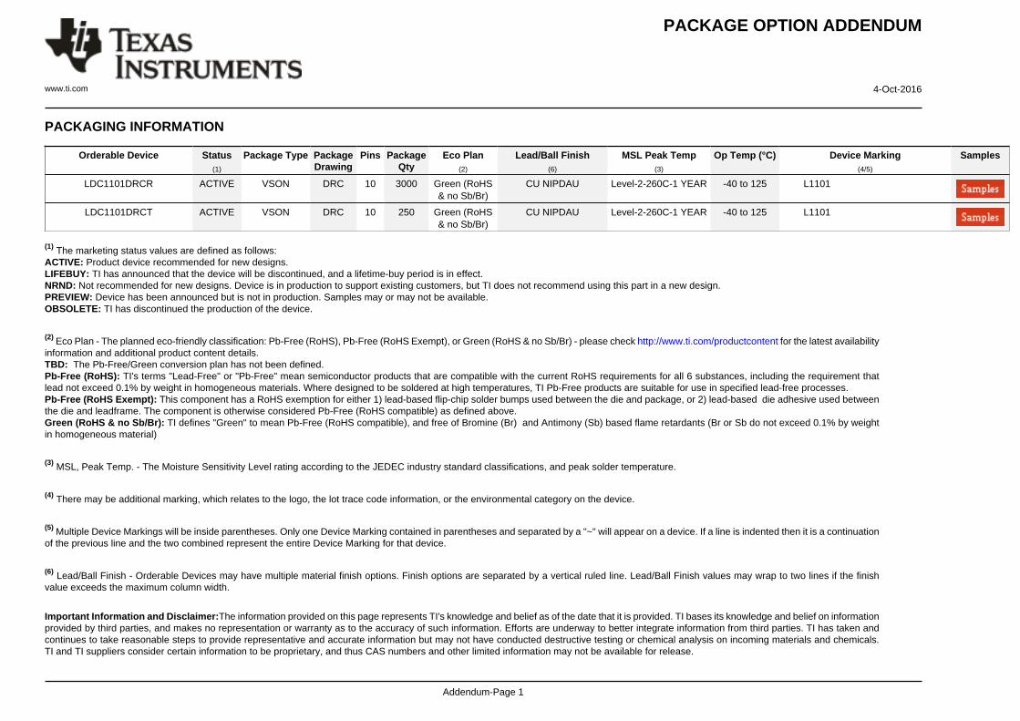
PACKAGE OPTION ADDENDUM
www.ti.com 4-Oct-2016
Addendum-Page 1
PACKAGING INFORMATION
Orderable Device Status(1)
Package Type PackageDrawing
Pins PackageQty
Eco Plan(2)
Lead/Ball Finish(6)
MSL Peak Temp(3)
Op Temp (°C) Device Marking(4/5)
Samples
LDC1101DRCR ACTIVE VSON DRC 10 3000 Green (RoHS& no Sb/Br)
CU NIPDAU Level-2-260C-1 YEAR -40 to 125 L1101
LDC1101DRCT ACTIVE VSON DRC 10 250 Green (RoHS& no Sb/Br)
CU NIPDAU Level-2-260C-1 YEAR -40 to 125 L1101
(1) The marketing status values are defined as follows:ACTIVE: Product device recommended for new designs.LIFEBUY: TI has announced that the device will be discontinued, and a lifetime-buy period is in effect.NRND: Not recommended for new designs. Device is in production to support existing customers, but TI does not recommend using this part in a new design.PREVIEW: Device has been announced but is not in production. Samples may or may not be available.OBSOLETE: TI has discontinued the production of the device.
(2) Eco Plan - The planned eco-friendly classification: Pb-Free (RoHS), Pb-Free (RoHS Exempt), or Green (RoHS & no Sb/Br) - please check http://www.ti.com/productcontent for the latest availabilityinformation and additional product content details.TBD: The Pb-Free/Green conversion plan has not been defined.Pb-Free (RoHS): TI's terms "Lead-Free" or "Pb-Free" mean semiconductor products that are compatible with the current RoHS requirements for all 6 substances, including the requirement thatlead not exceed 0.1% by weight in homogeneous materials. Where designed to be soldered at high temperatures, TI Pb-Free products are suitable for use in specified lead-free processes.Pb-Free (RoHS Exempt): This component has a RoHS exemption for either 1) lead-based flip-chip solder bumps used between the die and package, or 2) lead-based die adhesive used betweenthe die and leadframe. The component is otherwise considered Pb-Free (RoHS compatible) as defined above.Green (RoHS & no Sb/Br): TI defines "Green" to mean Pb-Free (RoHS compatible), and free of Bromine (Br) and Antimony (Sb) based flame retardants (Br or Sb do not exceed 0.1% by weightin homogeneous material)
(3) MSL, Peak Temp. - The Moisture Sensitivity Level rating according to the JEDEC industry standard classifications, and peak solder temperature.
(4) There may be additional marking, which relates to the logo, the lot trace code information, or the environmental category on the device.
(5) Multiple Device Markings will be inside parentheses. Only one Device Marking contained in parentheses and separated by a "~" will appear on a device. If a line is indented then it is a continuationof the previous line and the two combined represent the entire Device Marking for that device.
(6) Lead/Ball Finish - Orderable Devices may have multiple material finish options. Finish options are separated by a vertical ruled line. Lead/Ball Finish values may wrap to two lines if the finishvalue exceeds the maximum column width.
Important Information and Disclaimer:The information provided on this page represents TI's knowledge and belief as of the date that it is provided. TI bases its knowledge and belief on informationprovided by third parties, and makes no representation or warranty as to the accuracy of such information. Efforts are underway to better integrate information from third parties. TI has taken andcontinues to take reasonable steps to provide representative and accurate information but may not have conducted destructive testing or chemical analysis on incoming materials and chemicals.TI and TI suppliers consider certain information to be proprietary, and thus CAS numbers and other limited information may not be available for release.
PACKAGE OPTION ADDENDUM
www.ti.com 4-Oct-2016
Addendum-Page 2
In no event shall TI's liability arising out of such information exceed the total purchase price of the TI part(s) at issue in this document sold by TI to Customer on an annual basis.
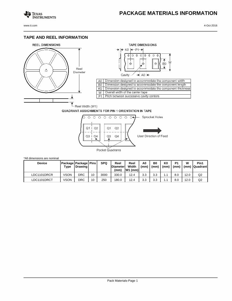
TAPE AND REEL INFORMATION
*All dimensions are nominal
Device PackageType
PackageDrawing
Pins SPQ ReelDiameter
(mm)
ReelWidth
W1 (mm)
A0(mm)
B0(mm)
K0(mm)
P1(mm)
W(mm)
Pin1Quadrant
LDC1101DRCR VSON DRC 10 3000 330.0 12.4 3.3 3.3 1.1 8.0 12.0 Q2
LDC1101DRCT VSON DRC 10 250 180.0 12.4 3.3 3.3 1.1 8.0 12.0 Q2
PACKAGE MATERIALS INFORMATION
www.ti.com 4-Oct-2016
Pack Materials-Page 1
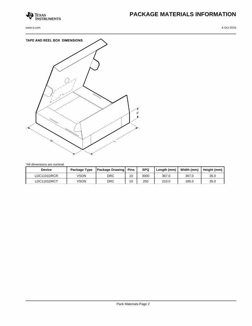
*All dimensions are nominal
Device Package Type Package Drawing Pins SPQ Length (mm) Width (mm) Height (mm)
LDC1101DRCR VSON DRC 10 3000 367.0 367.0 35.0
LDC1101DRCT VSON DRC 10 250 210.0 185.0 35.0
PACKAGE MATERIALS INFORMATION
www.ti.com 4-Oct-2016
Pack Materials-Page 2
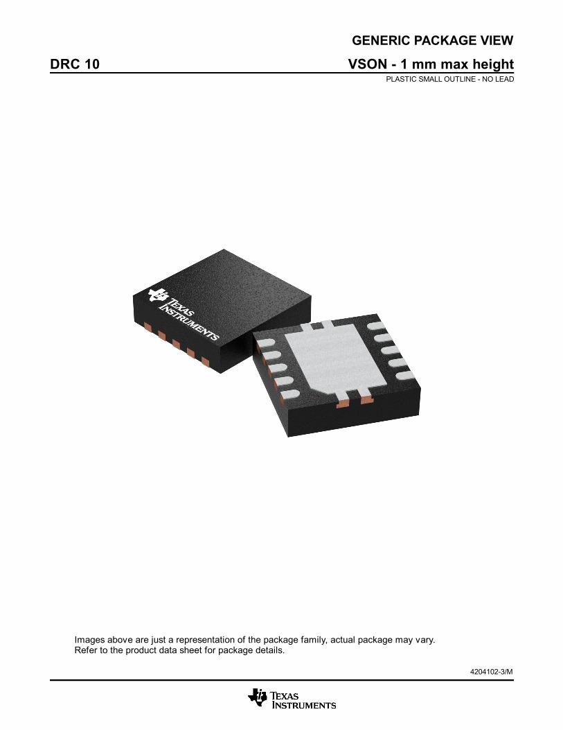
GENERIC PACKAGE VIEW
Images above are just a representation of the package family, actual package may vary.Refer to the product data sheet for package details.
DRC 10 VSON - 1 mm max heightPLASTIC SMALL OUTLINE - NO LEAD
4204102-3/M
www.ti.com
PACKAGE OUTLINE
C
10X 0.300.18
2.4 0.1
2X2
1.65 0.1
8X 0.5
1 MAX
10X 0.50.3
0.050.00
A 3.12.9
B
3.12.9
(0.2) TYP4X (0.25)
2X (0.5)
VSON - 1 mm max heightDRC0010JPLASTIC SMALL OUTLINE - NO LEAD
4218878/A 09/2017
PIN 1 INDEX AREA
SEATING PLANE
0.08 C
1
56
10
(OPTIONAL)PIN 1 ID 0.1 C A B
0.05 C
THERMAL PADEXPOSED
SYMM
SYMM11
NOTES: 1. All linear dimensions are in millimeters. Any dimensions in parenthesis are for reference only. Dimensioning and tolerancing per ASME Y14.5M. 2. This drawing is subject to change without notice. 3. The package thermal pad must be soldered to the printed circuit board for optimal thermal and mechanical performance.
SCALE 4.000

www.ti.com
EXAMPLE BOARD LAYOUT
0.07 MINALL AROUND
10X (0.25)
(2.4)
(2.8)
8X (0.5)
(1.65)
( 0.2) VIATYP
(0.575)
(0.95)
10X (0.6)
(R0.05) TYP
(3.4)
4X (0.25)
(0.5)
VSON - 1 mm max heightDRC0010JPLASTIC SMALL OUTLINE - NO LEAD
4218878/A 09/2017
SYMM
1
5 6
10
LAND PATTERN EXAMPLEEXPOSED METAL SHOWN
SCALE:20X
11SYMM
METAL UNDERSOLDER MASK
SOLDER MASKOPENING
NOTES: (continued) 4. This package is designed to be soldered to a thermal pad on the board. For more information, see Texas Instruments literature number SLUA271 (www.ti.com/lit/slua271).5. Vias are optional depending on application, refer to device data sheet. If any vias are implemented, refer to their locations shown on this view. It is recommended that vias under paste be filled, plugged or tented.
www.ti.com
EXAMPLE STENCIL DESIGN
(R0.05) TYP
10X (0.25)
10X (0.6)
2X (1.5)
2X(1.06)
(2.8)
(0.63)
8X (0.5)
(0.5)
4X (0.34)
4X (0.25)
(1.53)
VSON - 1 mm max heightDRC0010JPLASTIC SMALL OUTLINE - NO LEAD
4218878/A 09/2017
NOTES: (continued) 6. Laser cutting apertures with trapezoidal walls and rounded corners may offer better paste release. IPC-7525 may have alternate design recommendations.
SOLDER PASTE EXAMPLEBASED ON 0.125 mm THICK STENCIL
EXPOSED PAD 11:
80% PRINTED SOLDER COVERAGE BY AREASCALE:25X
SYMM
1
56
10
EXPOSED METALTYP
11
SYMM
SOLDER MASK OPENING
METAL UNDERSOLDER MASK
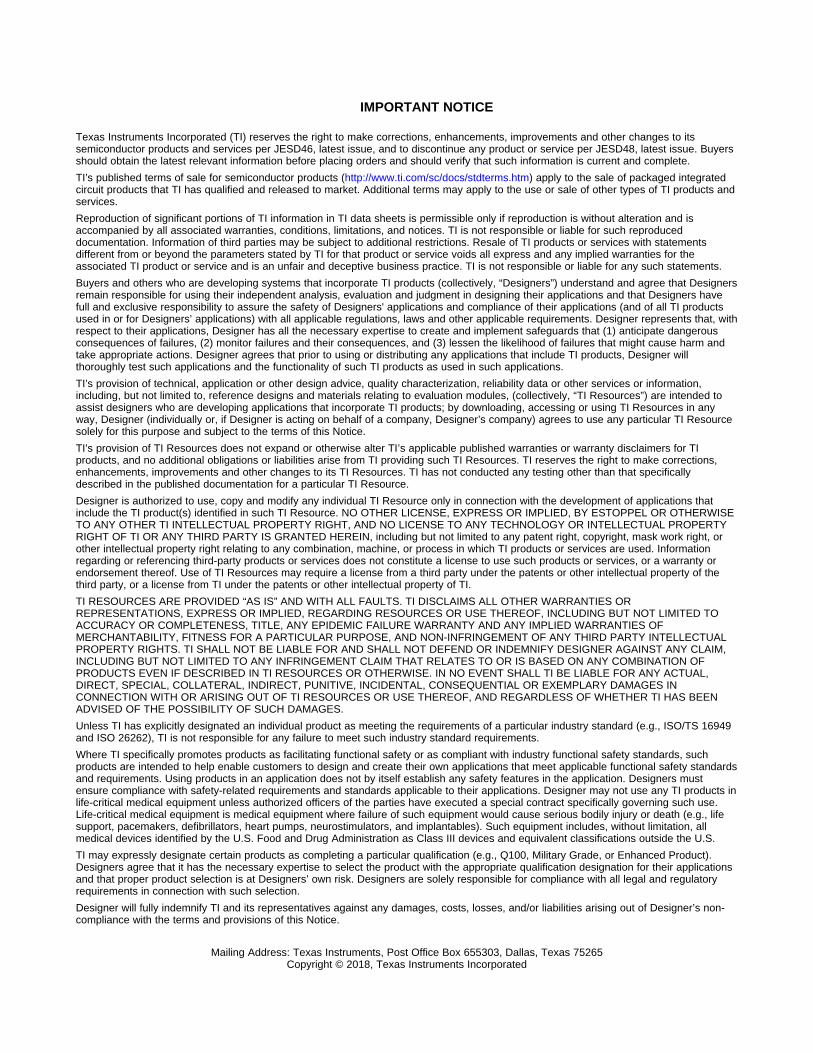
IMPORTANT NOTICE
Texas Instruments Incorporated (TI) reserves the right to make corrections, enhancements, improvements and other changes to itssemiconductor products and services per JESD46, latest issue, and to discontinue any product or service per JESD48, latest issue. Buyersshould obtain the latest relevant information before placing orders and should verify that such information is current and complete.TI’s published terms of sale for semiconductor products (http://www.ti.com/sc/docs/stdterms.htm) apply to the sale of packaged integratedcircuit products that TI has qualified and released to market. Additional terms may apply to the use or sale of other types of TI products andservices.Reproduction of significant portions of TI information in TI data sheets is permissible only if reproduction is without alteration and isaccompanied by all associated warranties, conditions, limitations, and notices. TI is not responsible or liable for such reproduceddocumentation. Information of third parties may be subject to additional restrictions. Resale of TI products or services with statementsdifferent from or beyond the parameters stated by TI for that product or service voids all express and any implied warranties for theassociated TI product or service and is an unfair and deceptive business practice. TI is not responsible or liable for any such statements.Buyers and others who are developing systems that incorporate TI products (collectively, “Designers”) understand and agree that Designersremain responsible for using their independent analysis, evaluation and judgment in designing their applications and that Designers havefull and exclusive responsibility to assure the safety of Designers' applications and compliance of their applications (and of all TI productsused in or for Designers’ applications) with all applicable regulations, laws and other applicable requirements. Designer represents that, withrespect to their applications, Designer has all the necessary expertise to create and implement safeguards that (1) anticipate dangerousconsequences of failures, (2) monitor failures and their consequences, and (3) lessen the likelihood of failures that might cause harm andtake appropriate actions. Designer agrees that prior to using or distributing any applications that include TI products, Designer willthoroughly test such applications and the functionality of such TI products as used in such applications.TI’s provision of technical, application or other design advice, quality characterization, reliability data or other services or information,including, but not limited to, reference designs and materials relating to evaluation modules, (collectively, “TI Resources”) are intended toassist designers who are developing applications that incorporate TI products; by downloading, accessing or using TI Resources in anyway, Designer (individually or, if Designer is acting on behalf of a company, Designer’s company) agrees to use any particular TI Resourcesolely for this purpose and subject to the terms of this Notice.TI’s provision of TI Resources does not expand or otherwise alter TI’s applicable published warranties or warranty disclaimers for TIproducts, and no additional obligations or liabilities arise from TI providing such TI Resources. TI reserves the right to make corrections,enhancements, improvements and other changes to its TI Resources. TI has not conducted any testing other than that specificallydescribed in the published documentation for a particular TI Resource.Designer is authorized to use, copy and modify any individual TI Resource only in connection with the development of applications thatinclude the TI product(s) identified in such TI Resource. NO OTHER LICENSE, EXPRESS OR IMPLIED, BY ESTOPPEL OR OTHERWISETO ANY OTHER TI INTELLECTUAL PROPERTY RIGHT, AND NO LICENSE TO ANY TECHNOLOGY OR INTELLECTUAL PROPERTYRIGHT OF TI OR ANY THIRD PARTY IS GRANTED HEREIN, including but not limited to any patent right, copyright, mask work right, orother intellectual property right relating to any combination, machine, or process in which TI products or services are used. Informationregarding or referencing third-party products or services does not constitute a license to use such products or services, or a warranty orendorsement thereof. Use of TI Resources may require a license from a third party under the patents or other intellectual property of thethird party, or a license from TI under the patents or other intellectual property of TI.TI RESOURCES ARE PROVIDED “AS IS” AND WITH ALL FAULTS. TI DISCLAIMS ALL OTHER WARRANTIES ORREPRESENTATIONS, EXPRESS OR IMPLIED, REGARDING RESOURCES OR USE THEREOF, INCLUDING BUT NOT LIMITED TOACCURACY OR COMPLETENESS, TITLE, ANY EPIDEMIC FAILURE WARRANTY AND ANY IMPLIED WARRANTIES OFMERCHANTABILITY, FITNESS FOR A PARTICULAR PURPOSE, AND NON-INFRINGEMENT OF ANY THIRD PARTY INTELLECTUALPROPERTY RIGHTS. TI SHALL NOT BE LIABLE FOR AND SHALL NOT DEFEND OR INDEMNIFY DESIGNER AGAINST ANY CLAIM,INCLUDING BUT NOT LIMITED TO ANY INFRINGEMENT CLAIM THAT RELATES TO OR IS BASED ON ANY COMBINATION OFPRODUCTS EVEN IF DESCRIBED IN TI RESOURCES OR OTHERWISE. IN NO EVENT SHALL TI BE LIABLE FOR ANY ACTUAL,DIRECT, SPECIAL, COLLATERAL, INDIRECT, PUNITIVE, INCIDENTAL, CONSEQUENTIAL OR EXEMPLARY DAMAGES INCONNECTION WITH OR ARISING OUT OF TI RESOURCES OR USE THEREOF, AND REGARDLESS OF WHETHER TI HAS BEENADVISED OF THE POSSIBILITY OF SUCH DAMAGES.Unless TI has explicitly designated an individual product as meeting the requirements of a particular industry standard (e.g., ISO/TS 16949and ISO 26262), TI is not responsible for any failure to meet such industry standard requirements.Where TI specifically promotes products as facilitating functional safety or as compliant with industry functional safety standards, suchproducts are intended to help enable customers to design and create their own applications that meet applicable functional safety standardsand requirements. Using products in an application does not by itself establish any safety features in the application. Designers mustensure compliance with safety-related requirements and standards applicable to their applications. Designer may not use any TI products inlife-critical medical equipment unless authorized officers of the parties have executed a special contract specifically governing such use.Life-critical medical equipment is medical equipment where failure of such equipment would cause serious bodily injury or death (e.g., lifesupport, pacemakers, defibrillators, heart pumps, neurostimulators, and implantables). Such equipment includes, without limitation, allmedical devices identified by the U.S. Food and Drug Administration as Class III devices and equivalent classifications outside the U.S.TI may expressly designate certain products as completing a particular qualification (e.g., Q100, Military Grade, or Enhanced Product).Designers agree that it has the necessary expertise to select the product with the appropriate qualification designation for their applicationsand that proper product selection is at Designers’ own risk. Designers are solely responsible for compliance with all legal and regulatoryrequirements in connection with such selection.Designer will fully indemnify TI and its representatives against any damages, costs, losses, and/or liabilities arising out of Designer’s non-compliance with the terms and provisions of this Notice.
Mailing Address: Texas Instruments, Post Office Box 655303, Dallas, Texas 75265Copyright © 2018, Texas Instruments Incorporated