Layout Design Guide - Single Board Computers (SBCs...
41
Layout Design Guide
Transcript of Layout Design Guide - Single Board Computers (SBCs...
Layout Design Guide

Layout Design Guide
Toradex AG l Altsagenstrasse 5 l 6048 Horw l Switzerland l +41 41 500 48 00 l www.toradex.com l [email protected] Page | 2
Issued by: Toradex Document Type: Design Guide
Purpose: This document is a guideline for designing a carrier board with high speed signals that is used
with Toradex Computer Modules.
Document
Version:
1.0
Revision History
Date
Version Remarks
14 April 2015 V1.0 Initial Release, based on section 2 of the Apalis Carrier Board Design
Guide V1.0
Layout Design Guide
Toradex AG l Altsagenstrasse 5 l 6048 Horw l Switzerland l +41 41 500 48 00 l www.toradex.com l [email protected] Page | 3
1 Introduction ....................................................................................................................... 4 1.1 Overview ............................................................................................................................. 4 1.2 Additional Documents .......................................................................................................... 4
1.2.1 Apalis Carrier Board Design Guide ............................................................................. 4 1.2.2 Apalis Module Datasheets ......................................................................................... 4 1.2.3 Apalis Module Definition ............................................................................................ 4 1.2.4 Colibri Carrier Board Design Guide ............................................................................. 4 1.2.5 Colibri Module Datasheets ......................................................................................... 5 1.2.6 Toradex Developer Centre ......................................................................................... 5 1.2.7 Carrier Board Design information ............................................................................... 5
1.3 Abbreviations ....................................................................................................................... 5
2 General Considerations ..................................................................................................... 8
3 PCB Stack-Up .................................................................................................................... 9 3.1 Four Layer Stack–Up ........................................................................................................... 9 3.2 Six Layer Stack–Up ........................................................................................................... 10 3.3 Eight Layer Stack–Up......................................................................................................... 10
4 Trace Impedance.............................................................................................................. 12
5 Component Placement and Schematic Optimizations ..................................................... 14
6 High-Speed Layout Considerations ................................................................................. 15 6.1 Power Supply .................................................................................................................... 15 6.2 Trace Bend Geometry ........................................................................................................ 17 6.3 Signal Proximity ................................................................................................................. 17 6.4 Trace Stubs ....................................................................................................................... 18 6.5 Ground Planes under Pads ................................................................................................. 18 6.6 Differential Pair Signals ...................................................................................................... 19 6.7 Length Matching ................................................................................................................ 21 6.8 Signal Return Path ............................................................................................................. 25 6.9 Analogue and Digital Ground .............................................................................................. 29
7 Layout Requirements of Interfaces .................................................................................. 32 7.1 PCI Express ...................................................................................................................... 33 7.2 SATA ................................................................................................................................ 33 7.3 Ethernet ............................................................................................................................ 34 7.4 USB .................................................................................................................................. 35 7.5 Parallel RGB LCD Interface ................................................................................................ 37 7.6 LVDS LCD Interface ........................................................................................................... 37 7.7 HDMI/DVI .......................................................................................................................... 38 7.8 Analogue VGA ................................................................................................................... 38 7.9 Parallel Camera Interface ................................................................................................... 39 7.10 SD/MMC/SDIO .................................................................................................................. 39 7.11 I
2C .................................................................................................................................... 40
7.12 Display Serial Interface (MIPI/DSI with D-PHY) .................................................................... 40 7.13 Camera Serial Interface (MIPI/CSI-2 with D-PHY) ................................................................ 40

Layout Design Guide
Toradex AG l Altsagenstrasse 5 l 6048 Horw l Switzerland l +41 41 500 48 00 l www.toradex.com l [email protected] Page | 4
1 Introduction
1.1 Overview
The latest Toradex Computer modules features new high speed interfaces such as PCI Express,
SATA, HDMI, USB 3.0, Ethernet, and LVDS which require special layout considerations regarding
trace impedance and length matching. Improper routing of such signals is a common pitfall in the
design of an Apalis or Colibri carrier board. This document helps avoiding layout problems that
can cause signal quality or EMC problems. Please read this document very carefully before you
start designing a carrier board.
Please use this document together with the design guide of the appropriate Toradex computer
module family and the datasheet of the module.
1.2 Additional Documents
1.2.1 Apalis Carrier Board Design Guide
This document provides additional information to the schematic design of a carrier board for the
Apalis modules. It contains reference schematics, descriptions of the power architecture and
information pertaining to the mechanical requirements of the module.
http://developer.toradex.com/hardware-resources/arm-family/carrier-board-design
1.2.2 Apalis Module Datasheets
There is a datasheet available for every Apalis Module. Amongst other things, this document
describes the type-specific interfaces and the secondary function of the pins. Before starting the
development of a customized carrier board, please check in this document whether the required
interfaces are really available on the selected modules.
https://www.toradex.com/products/apalis-arm-computer-modules
1.2.3 Apalis Module Definition
This document describes the Apalis Module standard. It provides additional information about the
interfaces.
http://docs.toradex.com/100240-apalis-module-specification.pdf
1.2.4 Colibri Carrier Board Design Guide
This document provides additional information about the schematic designs of carrier boards for
the Colibri modules. It contains reference schematics, description about the power architecture and
information related to the mechanical requirements of the module.
http://developer.toradex.com/hardware-resources/arm-family/carrier-board-design

Layout Design Guide
Toradex AG l Altsagenstrasse 5 l 6048 Horw l Switzerland l +41 41 500 48 00 l www.toradex.com l [email protected] Page | 5
1.2.5 Colibri Module Datasheets
There is a datasheet available for every Colibri Module. Amongst other things, this document
describes the additional interfaces and the secondary function of the pins. Before starting the
development of a customized carrier board, please refer this document to check if the required
interfaces are really available on the selected modules.
https://www.toradex.com/products/colibri-arm-computer-modules
1.2.6 Toradex Developer Centre
You can find a lot of additional information at the Toradex Developer Centre, which is updated
with the latest product support information on a regular basis.
Please note that the Developer Centre is common for all Toradex products. You should always
check to ensure if the information is valid or relevant for your specific module.
http://www.developer.toradex.com
1.2.7 Carrier Board Design information
We provide the complete schematics and the Altium project file for Apalis and Colibri Evaluation
Boards for free. This is a great help when designing your own Carrier Board.
http://developer.toradex.com/hardware-resources/arm-family/carrier-board-design
1.3 Abbreviations
Abbreviation Explanation
ADC Analogue to Digital Converter
AGND Analogue Ground - separate ground for analogue signals
Auto-MDIX Automatically Medium Dependent Interface Crossing - a PHY with Auto-MDIX is able to detect whether RX and TX need to be crossed (MDI or MDIX)
CAD Computer-Aided Design, in this document is referred to PCB Layout tools
CAN Controller Area Network - a bus that is manly used in automotive and industrial environment
CDMA Code Division Multiplex Access - an abbreviation often used for a mobile phone standard for data communication
CEC Consumer Electronic Control - a HDMI feature that allows to control CEC compatible devices
CPU Central Processing Unit
CSI Camera Serial Interface
DAC Digital to Analogue Converter
DDC Display Data Channel - an interface for reading out the capability of a monitor, in this document DDC2B (based on I
2C) is always meant
DRC Design Rule Check - a tool for checking whether all design rules are satisfied in a CAD tool
DSI Display Serial Interface
DVI Digital Visual Interface. Digital signals are electrical compatible with HDMI
DVI-A Digital Visual Interface Analogue only. Signals are compatible with VGA
DVI-D Digital Visual Interface Digital only. Signals are electrical compatible with HDMI
DVI-I Digital Visual Interface Integrated. Combines digital and analogue video signals in one connector
EDA Electronic Design Automation - software for schematic capture and PCB layout (CAD or ECAD)
EDID Extended Display Identification Data - timing setting information provided by the display in a PROM
EMC Electromagnetic Compatibility -theory of unintentional generation, propagation, and reception of electromagnetic energy
EMI Electromagnetic Interference - high frequency disturbances
eMMC Embedded Multi Media Card - flash memory combined with MMC interface controller in a BGA package, used as internal flash memory

Layout Design Guide
Toradex AG l Altsagenstrasse 5 l 6048 Horw l Switzerland l +41 41 500 48 00 l www.toradex.com l [email protected] Page | 6
Abbreviation Explanation
ESD Electrostatic Discharge - high voltage spike or spark that can damage electrostatic-sensitive devices
FPD-Link Flat Panel Display Link - high-speed serial interface for liquid crystal displays. In this document, also called LVDS interface.
GBE Gigabit Ethernet - Ethernet interface with a maximum data rate of 1000Mbit/s
GND Ground
GPIO General Purpose Input/Output pin that can be configured to be either an input or output
GSM Global System for Mobile Communications
HDA High Definition Audio (HD Audio) - digital audio interface between CPU and audio codec
HDCP High-Bandwidth Digital Content Protection - a copy protection system that is used by HDMI besides others
HDMI High-Definition Multimedia Interface - it combines audio and video signal for connecting monitors, TV sets or Projectors, electrical compatible with DVI-D
I2C Inter-Integrated Circuit- a two wire interface for connecting low speed peripherals
I2S Integrated Interchip Sound- a serial bus for connecting PCM audio data between two devices
IrDA Infrared Data Association - an infrared interface for connecting peripherals
JTAG Joint Test Action Group - widely used debug interface
LCD Liquid Crystal Display
LSB Least Significant Bit
LVDS
Low-Voltage Differential Signaling, electrical interface standard that can transport very high speed signals over twisted-pair cables. Many interfaces like PCIe or SATA use this interface. Since the first successful application was the Flat Panel Display Link, LVDS became a synonymous for this interface. In this document, the term LVDS is used for the FPD-Link interface.
MIPI Mobile Industry Processor Interface Alliance
MDI Medium Dependent Interface, physical interface between Ethernet PHY and cable connector
MDIX Medium Dependent Interface Crossed, an MDI interface with crossed RX and TX interfaces
mini PCIe PCI Express Mini Card, card form factor for internal peripherals. The interface features PCIe and USB 2.0 connectivity
MMC MultiMediaCard, flash memory card
MSB Most Significant Bit
mSATA Mini-SATA - a standardized form factor for small solid state drive, similar dimensions as mini PCIe
MXM3 Mobile PCI Express Module (second generation) - graphic card standard for mobile device. The Apalis form factor uses the physical connector but not the pin-out and the PCB dimensions of the MXM3 standard.
N/A Not Available
N/C Not Connected
OD Open Drain
OTG USB On-The-Go - a USB host interface that can also act as USB client when connected to another host interface
OWR One Wire (1-Wire) - low speed interface which needs just one data wire plus ground
PCB Printed Circuit Board
PCI Peripheral Component Interconnect - parallel computer expansion bus for connecting peripherals
PCIe PCI Express - high-speed serial computer expansion bus that replaces the PCI bus
PCM Pulse-Code Modulation - digitally representation of analogue signals. Standard interface for digital audio
PD Pull Down Resistor
PHY Physical Layer of the OSI model
PMIC Power Management IC, integrated circuit that manages amongst others the power sequence of a system
PU Pull-Up Resistor
PWM Pulse-Width Modulation
RGB Red Green Blue - color channels in common display interfaces
RJ45 Registered Jack - a common name for the 8P8C modular connector that is used for Ethernet wiring
RS232 Single ended serial port interface
RS422 Differential signaling serial port interface, full duplex
RS485 Differential signaling serial port interface, half duplex, multi drop configuration possible
R-UIM Removable User Identity Module - identifications card for CDMA phones and networks, an extension of the GSM SIM card

Layout Design Guide
Toradex AG l Altsagenstrasse 5 l 6048 Horw l Switzerland l +41 41 500 48 00 l www.toradex.com l [email protected] Page | 7
Abbreviation Explanation
S/PDIF Sony/Philips Digital Interconnect Format - optical or coaxial interface for audio signals
SATA Serial ATA - high speed differential signaling interface for hard drives and SSD
SD Secure Digital - flash memory card
SDIO Secure Digital Input Output - an external bus for peripherals that uses the SD interface
SIM Subscriber Identification Module - identification card for GSM phones
SMBus System Management Bus (SMB) -, two wire bus based on the I
2C specifications, used specially in x86
design for system management.
SoC System on a Chip - IC which integrates the main component of a computer on a single chip
SPI Serial Peripheral Interface Bus - synchronous four wire full duplex bus for peripherals
TIM Thermal Interface Material - thermal conductive material between CPU and heat spreader or heat sink
TMDS Transition-Minimized Differential Signaling - serial high speed transmitting technology that is used by DVI and HDMI
TVS Diode Transient-Voltage-Suppression Diode - diode that is used to protect interfaces against voltage spikes
UART Universal Asynchronous Receiver/Transmitter - serial interface, in combination with a transceiver a RS232, RS422, RS485, IrDA or similar interface can be achieved
USB Universal Serial Bus - serial interface for internal and external peripherals
VCC Positive supply voltage
VGA Video Graphics Array - analogue video interface for monitors
Table 1: Abbreviations

Layout Design Guide
Toradex AG l Altsagenstrasse 5 l 6048 Horw l Switzerland l +41 41 500 48 00 l www.toradex.com l [email protected] Page | 8
2 General Considerations
The Apalis and Colibri modules feature a range of high speed interfaces which need special
treatment with regards to its PCB layout. This section describes a collection of basic rules to follow.
It should be noted however that it is not often possible to follow all the rules. It is the job of the
design engineer, with the aid of this design guide, to decide which rules can be violated, in what
area, for which signals, and when it is necessary to do so.
The interfaces have an ‘importance priority’ over one another when it comes to ensuring optimal
routing of designs. The below-mentioned list describes the importance priority of the signals. PCIe
is the first one on the list and has the highest priority, and should be routed with special care.
Signals continue to be ordered with descending priority and as such become less problematic with
respect to layout and routing. Often, a good approach to take is to layout and route interfaces in
order of their importance priority, from high to low.
1. PCI Express
2. USB 3.0 (Super Speed signals)
3. SATA
4. Ethernet
5. HDMI
6. LVDS Display
7. USB 2.0
8. SD/MMC/SDIO
9. Parallel RGB LCD Interface
10. Parallel Camera Input
11. HD Audio
12. Analogue VGA
13. Analogue Audio, ADC Inputs, Touch Panel
14. Low Speed Interfaces (I2C, UART, SPI, CAN, PWM, OWR, S/PDIF, Keypad, GPIO)

Layout Design Guide
Toradex AG l Altsagenstrasse 5 l 6048 Horw l Switzerland l +41 41 500 48 00 l www.toradex.com l [email protected] Page | 9
3 PCB Stack-Up
In order to reduce reflections at high speed signals, it is necessary to match the impedance
between source, sink, and transmission line. The impedance of a signal trace depends on its
geometry and its position with respect to any reference planes. The trace width and spacing
between differential pairs for a specific impedance requirement is dependent on the chosen PCB
stack-up. As there are limitations in the minimum trace width and spacing which depends on the
type of PCB technology and cost requirements, a PCB stack-up needs to be chosen which allows all
the required impedances to be realized. The presented stack-ups in the following subsections are
intended as examples which can be used as a starting point for helping in stackup evaluation and
selection. If a different stack-up is required other than those shown in the examples, please
recalculate the dimensions of the traces. Work closely with your PCB manufacturer when selecting
suitable stack-up solution.
3.1 Four Layer Stack–Up
Figure 1: Four Layer PCB Stack-Up Example
The high speed signals on the top layer are referenced to the ground plane on layer 2. Since the
references for the high-speed signals on the bottom layer are the power planes on Layer 3, it is
necessary to place stitching capacitors between the aforementioned power planes and ground.
More information about stitching capacitors can be found in section 6.8. In this stack-up, it is
preferential to route high speed signals on the top layer as opposed to the bottom layer so that the
signals have a direct reference to the ground layer. For some designs it may be desirable to have
the bottom layer as primary high speed routing layer. In this case, the power and ground usage on
Layer 2 and 3 could be swapped.
SoldermaskHigh Speed Signals
Prepreg
GND Plane
Power Plane
Core
Prepreg
High Speed SignalsSoldermask
PTH
Via
20µm43µm
112µm
18µm
18µm
1180µm
112µm
43µm20µm
Top Layer 1
Layer 2
Layer 3
Bottom Layer 4
Total: 1600µm

Layout Design Guide
Toradex AG l Altsagenstrasse 5 l 6048 Horw l Switzerland l +41 41 500 48 00 l www.toradex.com l [email protected] Page | 10
3.2 Six Layer Stack–Up
Figure 2: Six Layer PCB Stack-Up Example
In this example, the reference planes for the high-speed signals on the top layer are the power
planes on layer 2. Stitching capacitors from their associated reference power planes to the ground
is therefore required. More information about stitching capacitors can be found in section 6.8. The
signal reference for the bottom layer is the ground plane on layer 5. In this stack-up, it is
preferable to route high-speed signals on the bottom layer. As in the previous example, power and
ground layers could be swapped if it is desirable to have the primary high-speed routing layer on
the top layer.
The reference planes for signals on Layer 3 are located on Layer 2 and 5. The same reference
planes are used by signals routed on Layer 4. As the reference planes are on layers which have a
relatively large distance from Signal Layers 3 and 4, the traces would need to be very wide in order
to achieve a common impedance of 50Ω. Therefore, these layers are not suitable for routing high-
speed signals. In this stack-up approach, Layers 3 and 4 can only be used for routing low-speed
signals where impedance matching is not required.
3.3 Eight Layer Stack–Up
Figure 3: Eight Layer PCB Stack-Up Example
SoldermaskHigh Speed Signals
Low Speed Signals
Core
Prepreg
High Speed SignalsSoldermask
20µm35µm
18µm
410µm
400µm
35µm20µm
Top Layer 1
Layer 3
Bottom Layer 6
Total: 1600µm
Prepreg 112µm
Power Plane 18µm
GND Plane
Core
18µm
410µm
Low Speed Signals 18µm
Prepreg 112µm
PTH
Via
Layer 2
Layer 4
Layer 5
SoldermaskHigh Speed Signals
PrepregGND Plane
Power Plane
Core
Prepreg
High Speed SignalsSoldermask
20µm35µm
112µm18µm
18µm
200µm
400µm
35µm20µm
Top Layer 1
Layer 2
Layer 4
Bottom Layer 8
Total: 1600µm
Prepreg 190µm
High Speed Signals 18µm
High Speed Signals
Core
18µm
200µm
GND Plane 18µm
Prepreg 190µm
GND Plane 18µmPrepreg 112µm
PTH
Via
Layer 3
Layer 5
Layer 6
Layer 7
Layout Design Guide
Toradex AG l Altsagenstrasse 5 l 6048 Horw l Switzerland l +41 41 500 48 00 l www.toradex.com l [email protected] Page | 11
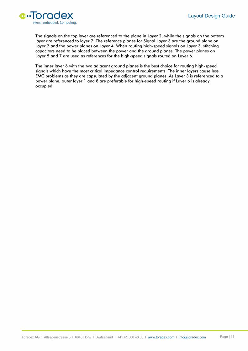
The signals on the top layer are referenced to the plane in Layer 2, while the signals on the bottom
layer are referenced to layer 7. The reference planes for Signal Layer 3 are the ground plane on
Layer 2 and the power planes on Layer 4. When routing high-speed signals on Layer 3, stitching
capacitors need to be placed between the power and the ground planes. The power planes on
Layer 5 and 7 are used as references for the high-speed signals routed on Layer 6.
The inner layer 6 with the two adjacent ground planes is the best choice for routing high-speed
signals which have the most critical impedance control requirements. The inner layers cause less
EMC problems as they are capsulated by the adjacent ground planes. As Layer 3 is referenced to a
power plane, outer layer 1 and 8 are preferable for high-speed routing if Layer 6 is already
occupied.

Layout Design Guide
Toradex AG l Altsagenstrasse 5 l 6048 Horw l Switzerland l +41 41 500 48 00 l www.toradex.com l [email protected] Page | 12
4 Trace Impedance
Care should be taken to distinguish between single-ended and differential trace impedance. High-
speed single ended signals such as the parallel RGB LCD or camera interface need to be routed
with the specified single-ended impedance. This is the impedance between the trace and the
reference ground.
High-speed differential pair signals such as PCIe, SATA, USB, HDMI etc. need to be routed with
differential impedance. This is the impedance between the two signal traces of a pair. As the
signals are also referenced to ground, each differential pair signal also has single-ended
impedance. When selecting trace geometry, priority should be given to matching the differential
impedance over the single-ended impedance. The differential impedance is always smaller than
twice the single ended impedance
𝑍𝐷𝑖𝑓𝑓𝑒𝑟𝑛𝑡𝑖𝑎𝑙 < 2 ∙ 𝑍𝑆𝑖𝑛𝑔𝑙𝑒 𝐸𝑛𝑑𝑒𝑑
The signals allow a certain impedance tolerance (e.g. 50Ω ±15%). When defining trace geometry,
try to keep the calculated impedance value as close as possible to the exact impedance value. This
allows greater flexibility during PCB manufacture. Variation in impedances will occur between
different production lots. If the calculated impedance is in the middle of the tolerance band, it will
help ensure the maximum production yield.
Different tools can be used for calculating the trace impedance. Polar Instruments offers a widely
used tool. Many PCB manufacturers use this tool. PCB manufacturers can often help customers
with impedance calculations, and it is suggested that you work with your chosen PCB manufacturer
during your design. Many PCB layout tools offer a very basic impedance calculator. Unfortunately,
these calculators are not reliable for all situations.
Traces on the top or bottom layer have only one reference plane. These traces are called
Microstrip. The following figure shows the geometry of such Microstrips. H1 is the distance from the
trace to the according reference plane. Er1 is the relative permittivity of the isolation material. The
traces have a trapezoid form due to the etching process. In the layout tool, the traces have to be
designed with a width of W1. W2 depends on the trace height (T1) and the duration of the etching.
Contact your PCB manufacturer in order to get the information about the resulting width W2. S1 is
the spacing within a differential pair.
Figure 4: Trace Geometry of Microstrips
Traces in the inner layer of a PCB have two reference planes, reducing electromagnetic emissions
and increasing immunity to external noise sources. These traces are called striplines. The following
figure shows the geometry of such striplines. When making impedance calculation of striplines,
special care needs to be taken when it comes to the isolation thickness H1 and H2. H1 is the
thickness of the core material. The traces are embedded in the prepreg material. As the traces
have a finite height, the prepreg height H2 depends on the copper density. The relative permittivity
of the core and prepreg material can be slightly different. Many impedance calculation tools can
take this in account.
Er1 (Prepreg)
Reference Plane
H1
T1W2
W1
Reference Plane
H1
T1W2
W1
S1
Er1 (Prepreg)
Single Ended Impedance of Microstrip Differential Impedance of Microstrip

Layout Design Guide
Toradex AG l Altsagenstrasse 5 l 6048 Horw l Switzerland l +41 41 500 48 00 l www.toradex.com l [email protected] Page | 13
Figure 5: Trace Geometry of Striplines
The following table shows typical trace geometries for traces using the four layer stack-up,
presented in section 3.
Signal Type Required ZSingle Ended
Required ZDifferential
Layer Trace Type W1 S1
Common Single Ended 50Ω N/A 1, 4 Microstrip 180µm N/A
PCIe, USB, HDMI, 50Ω 90Ω 1, 4 Microstrip 180µm 190µm
SATA 55Ω 90Ω 1, 4 Microstrip 150µm 150µm
Ethernet 55Ω 95Ω 1, 4 Microstrip 150µm 165µm
LVDS 55Ω 100Ω 1, 4 Microstrip 150µm 200µm
Table 2: Four Layer Stack-Up Example
The following table shows typical trace geometries for traces using the six layer stack-up, presented
in section 3.
Signal Type Required ZSingle Ended
Required ZDifferential
Layer Trace Type W1 S1
Common Single Ended 50Ω N/A 1, 6 Microstrip 180µm N/A
PCIe, USB, HDMI, 50Ω 90Ω 1, 6 Microstrip 180µm 200µm
SATA 55Ω 90Ω 1, 6 Microstrip 150µm 130µm
Ethernet 55Ω 95Ω 1, 6 Microstrip 150µm 165µm
LVDS 55Ω 100Ω 1, 6 Microstrip 150µm 200µm
Table 3: Six Layer Stack-Up Example
The following table shows typical trace geometries for traces used in the eight layer stack-up,
presented in section 3.
Signal Type Required ZSingle Ended
Required ZDifferential
Layer Trace Type W1 S1
Common Single Ended 50Ω N/A 1, 8 Microstrip 180µm N/A
3, 6 Stripline 170µm N/A
PCIe, USB, HDMI, 50Ω 90Ω 1, 8 Microstrip 180µm 200µm
3, 6 Stripline 170µm 185µm
SATA 55Ω 90Ω 1, 8 Microstrip 150µm 130µm
3, 6 Stripline 140µm 120µm
Ethernet 55Ω 95Ω 1, 8 Microstrip 150µm 165µm
3, 6 Stripline 140µm 155µm
LVDS 55Ω 100Ω 1, 8 Microstrip 150µm 200µm
3, 6 Stripline 140µm 200µm
Table 4: Eight Layer Stack-Up Example
Reference Plane
H1
T1W2
W1
Reference Plane
H1
T1W2
W1
S1
Reference Plane Reference Plane
H2
H2
Er2 (Prepreg)
Er1 (Core)
Er2 (Prepreg)
Er1 (Core)
Single Ended Impedance of Stripline Differential Impedance of Stripline
Layout Design Guide
Toradex AG l Altsagenstrasse 5 l 6048 Horw l Switzerland l +41 41 500 48 00 l www.toradex.com l [email protected] Page | 14
5 Component Placement and Schematic Optimizations
The placement of the components is very often an underestimated subtask of the PCB design.
Problems with signal return paths (see section 6.8) are very often related to suboptimal placement
of the components. If a signal needs to cross a splitting of its reference plane, one should first
check whether this splitting is really unavoidable. Quite often, the solution can be a better
placement of the components.
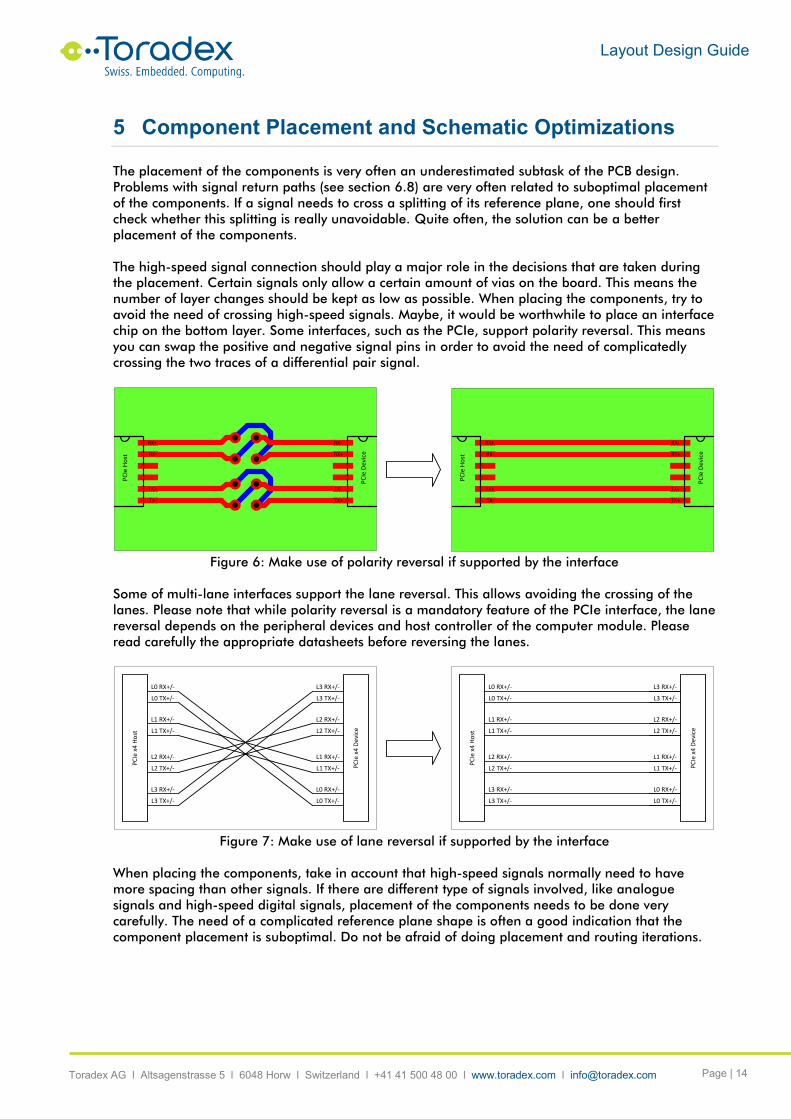
The high-speed signal connection should play a major role in the decisions that are taken during
the placement. Certain signals only allow a certain amount of vias on the board. This means the
number of layer changes should be kept as low as possible. When placing the components, try to
avoid the need of crossing high-speed signals. Maybe, it would be worthwhile to place an interface
chip on the bottom layer. Some interfaces, such as the PCIe, support polarity reversal. This means
you can swap the positive and negative signal pins in order to avoid the need of complicatedly
crossing the two traces of a differential pair signal.
Figure 6: Make use of polarity reversal if supported by the interface
Some of multi-lane interfaces support the lane reversal. This allows avoiding the crossing of the
lanes. Please note that while polarity reversal is a mandatory feature of the PCIe interface, the lane
reversal depends on the peripheral devices and host controller of the computer module. Please
read carefully the appropriate datasheets before reversing the lanes.
Figure 7: Make use of lane reversal if supported by the interface
When placing the components, take in account that high-speed signals normally need to have
more spacing than other signals. If there are different type of signals involved, like analogue
signals and high-speed digital signals, placement of the components needs to be done very
carefully. The need of a complicated reference plane shape is often a good indication that the
component placement is suboptimal. Do not be afraid of doing placement and routing iterations.
RX+
PC
Ie H
ost
PC
Ie D
evic
eRX-
TX+
TX-
RX-
RX+
TX-
TX+
RX+
PC
Ie H
ost
PC
Ie D
evic
eRX-
TX+
TX-
RX-
RX+
TX-
TX+
PC
Ie x
4 H
ost
PC
Ie x
4 D
evic
e
L0 RX+/-
L0 TX+/-
L1 RX+/-
L1 TX+/-
L2 RX+/-
L2 TX+/-
L3 RX+/-
L3 TX+/-
L3 RX+/-
L3 TX+/-
L2 RX+/-
L2 TX+/-
L1 RX+/-
L1 TX+/-
L0 RX+/-
L0 TX+/-
PC
Ie x
4 H
ost
PC
Ie x
4 D
evic
eL0 RX+/-
L0 TX+/-
L1 RX+/-
L1 TX+/-
L2 RX+/-
L2 TX+/-
L3 RX+/-
L3 TX+/-
L3 RX+/-
L3 TX+/-
L2 RX+/-
L2 TX+/-
L1 RX+/-
L1 TX+/-
L0 RX+/-
L0 TX+/-

Layout Design Guide
Toradex AG l Altsagenstrasse 5 l 6048 Horw l Switzerland l +41 41 500 48 00 l www.toradex.com l [email protected] Page | 15
6 High-Speed Layout Considerations
6.1 Power Supply
Digital circuits often draw a non-continuous current from their supply power. Peak current
consumption can be relatively large with high frequency components. If the supply traces are long,
such current peaks can cause high frequency noise emission, which can be introduced into other
signals. As traces have parasitic resistance and inductance, this high frequency noise can be
coupled into supplies for other circuits (see left figure below). Another problem is that the parasitic
inductance of the supply trace reduces the ability for the trace to carry the current peaks, which can
cause voltage drops at the consuming circuit. It is therefore necessary to add bypass capacitors to
the power input pins of digital circuits, which act to provide a reservoir of energy that can be drawn
on to help supply the short term peak currents that may be required.
Figure 8: Add bypass capacitors
If possible, individual bypass capacitors should be placed on every power supply pin of an
integrated circuit. If supply pins are close together, a bypass capacitor may be shared between
both pins. Capacitors should be placed as close as possible to supply pins. Try to enlarge the
supply trace widths. Try to keep the traces short. Current flow direction should also be considered.
It is preferable that the current first passes the bypass capacitor and then enters the supply pin.
Add an adequate amount of vias to the power supply traces. As a rule of thumb, place one via for
one ampere of current consumption. If the decoupling capacitors are placed on the other side of
the PCB and the current needs to go through vias, also consider the peak current. Also, do not
forget about the ground return current. The ground should have at least the same amount of vias
as the supply.
Figure 9: Place Bypass Capacitors close to IC pins
Large capacitors have a limitation in the speed they can provide energy to counter the current
peaks, while small capacitors may not have enough capacity to satisfy the energy demand.
Therefore, often a combination of small and big (e.g. 100nF + 10 µF) capacitors is a good choice
for such supply circuits. Ensure that the smaller capacitor is placed closer to the supply pin than the
bigger one.
Digital Cricuit 1
Digital Cricuit 2
DigitalSupply
ID2+ΔiD2ID1+ΔiD1+ID2+ΔiD2
Parasitic Resistance andIncuctance of Traces
Digital Cricuit 1
Digital Cricuit 2
DigitalSupply
ID2ID1+ID2
Parasitic Resistance andIncuctance of Traces
ΔiD1 ΔiD2
Bypass Capacitor
Bypass Capacitor
GND
VCC
10
0n
F
10
µF
GND
VCC
GND
10
0n
F
10
µF
VCC
GND
VCC
GND GND
VCC
10
0n
F
10
µF
GND
VCC
GND
VCC
GND
Layout Design Guide
Toradex AG l Altsagenstrasse 5 l 6048 Horw l Switzerland l +41 41 500 48 00 l www.toradex.com l [email protected] Page | 16
If buck or boost converters are used on the baseboard, make sure that its layout follows the
recommendations of the supplier.
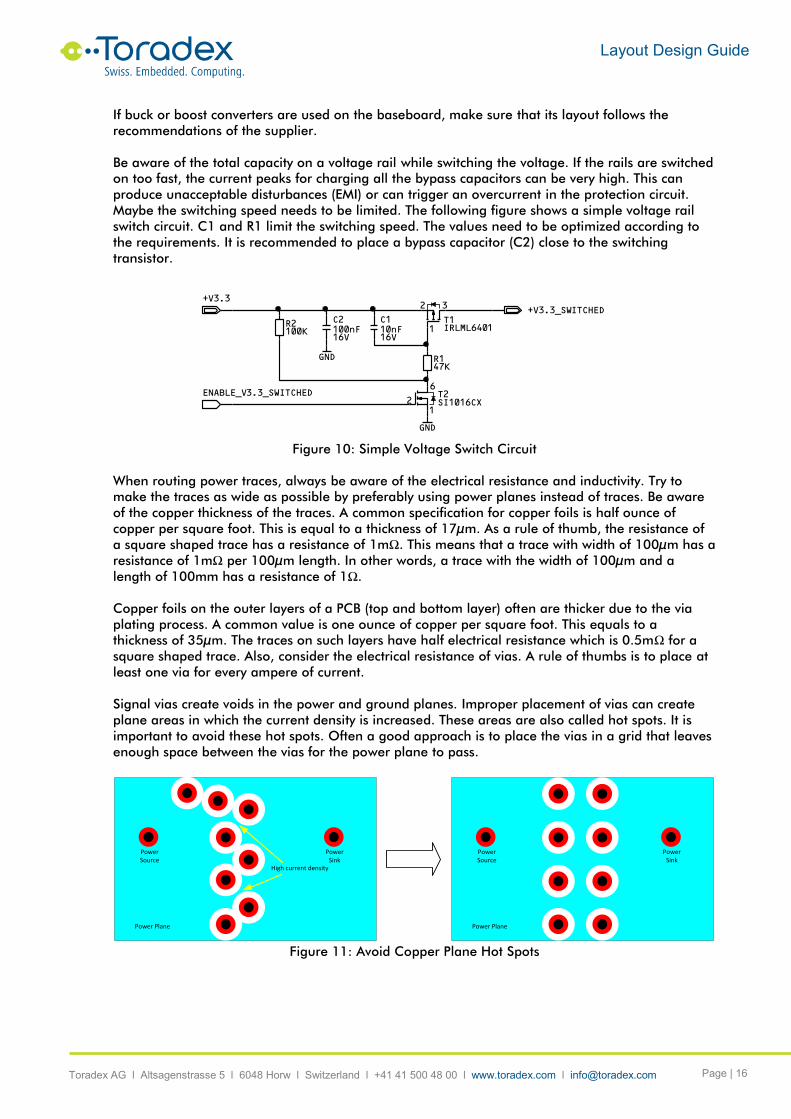
Be aware of the total capacity on a voltage rail while switching the voltage. If the rails are switched
on too fast, the current peaks for charging all the bypass capacitors can be very high. This can
produce unacceptable disturbances (EMI) or can trigger an overcurrent in the protection circuit.
Maybe the switching speed needs to be limited. The following figure shows a simple voltage rail
switch circuit. C1 and R1 limit the switching speed. The values need to be optimized according to
the requirements. It is recommended to place a bypass capacitor (C2) close to the switching
transistor.
Figure 10: Simple Voltage Switch Circuit
When routing power traces, always be aware of the electrical resistance and inductivity. Try to
make the traces as wide as possible by preferably using power planes instead of traces. Be aware
of the copper thickness of the traces. A common specification for copper foils is half ounce of
copper per square foot. This is equal to a thickness of 17µm. As a rule of thumb, the resistance of
a square shaped trace has a resistance of 1mΩ. This means that a trace with width of 100µm has a
resistance of 1mΩ per 100µm length. In other words, a trace with the width of 100µm and a
length of 100mm has a resistance of 1Ω.
Copper foils on the outer layers of a PCB (top and bottom layer) often are thicker due to the via
plating process. A common value is one ounce of copper per square foot. This equals to a
thickness of 35µm. The traces on such layers have half electrical resistance which is 0.5mΩ for a
square shaped trace. Also, consider the electrical resistance of vias. A rule of thumbs is to place at
least one via for every ampere of current.
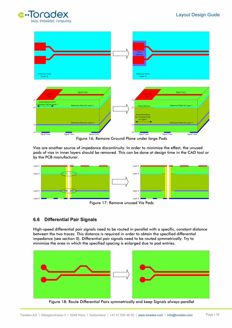
Signal vias create voids in the power and ground planes. Improper placement of vias can create
plane areas in which the current density is increased. These areas are also called hot spots. It is
important to avoid these hot spots. Often a good approach is to place the vias in a grid that leaves
enough space between the vias for the power plane to pass.
Figure 11: Avoid Copper Plane Hot Spots
T2SI1016CX
6
21
R147K
R2100K 10nF
16V
C1
GND
C2
16V100nF
T1IRLML6401
3
1
2+V3.3_SWITCHED
GND
+V3.3
ENABLE_V3.3_SWITCHED
Power Source
Power Sink
Power Plane
Power Source
Power Sink
Power Plane
High current density

Layout Design Guide
Toradex AG l Altsagenstrasse 5 l 6048 Horw l Switzerland l +41 41 500 48 00 l www.toradex.com l [email protected] Page | 17
6.2 Trace Bend Geometry
When routing high-speed signals, bends should be minimized. If bends are needed, use 135°
bends instead of 90°.
Figure 12: Use 135° Bends instead of 90°
Serpentine traces (also called meander) are often needed when a certain trace length needs to be
achieved. Keep a minimum distance of four times the trace width between adjacent copper in a
single trace. The individual segments of the bends should be at least 1.5 times the trace width. A
lot of DRCs in CAD tools do not check these minimum distances as the traces are part of the same
net.
Figure 13: Keep minimum Distance and Segment Length at Bends
6.3 Signal Proximity
Information about the required minimum distance between high-speed signals can be found in
section 0. A minimum distance is required in order to minimize crosstalk between traces. The level
of crosstalk depends on the distance between two traces and the length in which they are closely
routed. Sometimes, bottlenecks can force the routing of traces closer than to what is normally
permitted. Try to minimize such areas and enlarge the distance between the signals outside the
bottleneck. If there is space available, try to enlarge the distance between the high speed-signals
(and between high-speed and low-speed signals) even if the minimum trace separation
requirement has been met.
>4x trace width
>1.5x trace width
>1.5x tracewidth

Layout Design Guide
Toradex AG l Altsagenstrasse 5 l 6048 Horw l Switzerland l +41 41 500 48 00 l www.toradex.com l [email protected] Page | 18
Figure 14: Try to increase Spacing between Traces whenever it is possible
6.4 Trace Stubs
Long stub traces can act as antennas and therefore increase problems complying with EMC
standards. Stub traces can also produce reflections which negatively impacts signal integrity.
Common sources for stubs are pull-up or pull-down resistors on high speed signals. If such
resistors are required, route the signals as a daisy chain.
Figure 15: Avoid Stub Traces by Daisy Chain Routing
As a rule of thumb, stubs longer than a tenth of the wavelength should be considered as
problematic. The following example shows the calculations on a Gen3 PCIe signal:
𝑙𝑀𝐴𝑋 ≪1
10𝜆𝑀𝐼𝑁 =
𝑣
10 ∙ 𝑓𝑀𝐴𝑋
=
𝑐
√𝜀𝑟
10 ∙ 𝑓𝑀𝐴𝑋
=
300 ∙ 106 𝑚𝑠⁄
√4.510 ∙ 4𝐺𝐻𝑧
= 3.5𝑚𝑚
Vias can also act as stubs. For example, in a six layer board, when a signal changes from layer 1 to
3 by using a via, the via creates a stub which reaches layer 6. Back-drilling the vias in order to
avoid such stubs is a quite expensive technology and one which is not supported by most PCB
manufacturers. The only practical solution is to reduce the number of vias in high-speed traces.
6.5 Ground Planes under Pads
The impedance of a trace depends on its width and the distance between trace and reference
plane. A wide trace has lower impedance than a thin one with the same distance. The same effect
also exists for connector and component pads. A large pad has significantly lower impedance than
the trace which is connected to the pad. This impedance discontinuity can cause reflections reduces
signal integrity. Therefore, under large connector and component pads, a plane obstruct should be
placed. In this case, an active reference plane should be placed on another layer. This reference
plane needs to be stitched with vias to the normal reference plane.
Layout Design Guide
Toradex AG l Altsagenstrasse 5 l 6048 Horw l Switzerland l +41 41 500 48 00 l www.toradex.com l [email protected] Page | 19
Figure 16: Remove Ground Plane under large Pads
Vias are another source of impedance discontinuity. In order to minimize the effect, the unused
pads of vias in inner layers should be removed. This can be done at design time in the CAD tool or
by the PCB manufacturer.
Figure 17: Remove unused Via Pads
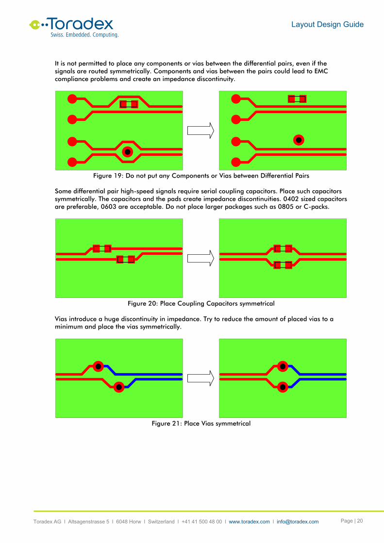
6.6 Differential Pair Signals
High-speed differential pair signals need to be routed in parallel with a specific, constant distance
between the two traces. This distance is required in order to obtain the specified differential
impedance (see section 0). Differential pair signals need to be routed symmetrically. Try to
minimize the area in which the specified spacing is enlarged due to pad entries.
Figure 18: Route Differential Pairs symmetrically and keep Signals always parallel
Reference Plane (Layer 2)
Connector Pad
Signal Trace Signal TraceSignal Trace
Plane Obstruct Reference Plane for Layer 1
Reference Plane for Layer 4
L1
L2
L3
L4
Active Reverence for Connector Pad
on Layer 1
Signal TraceConnector
Pad
Reference Plane (Layer 2)
PlaneObstruct
Connector Pad
Signal Trace Signal TraceSignal Trace
Reference Plane for Layer 1
Reference Plane for Layer 4
L1
L2
L3
L4
Active Reverence for Connector Pad on Layer 1
Signal TraceConnector
Pad
Layer 1
Layer 2
Layer 3
Layer 4
Layer 1
Layer 2
Layer 3
Layer 4
Layout Design Guide
Toradex AG l Altsagenstrasse 5 l 6048 Horw l Switzerland l +41 41 500 48 00 l www.toradex.com l [email protected] Page | 20
It is not permitted to place any components or vias between the differential pairs, even if the
signals are routed symmetrically. Components and vias between the pairs could lead to EMC
compliance problems and create an impedance discontinuity.
Figure 19: Do not put any Components or Vias between Differential Pairs
Some differential pair high-speed signals require serial coupling capacitors. Place such capacitors
symmetrically. The capacitors and the pads create impedance discontinuities. 0402 sized capacitors
are preferable, 0603 are acceptable. Do not place larger packages such as 0805 or C-packs.
Figure 20: Place Coupling Capacitors symmetrical
Vias introduce a huge discontinuity in impedance. Try to reduce the amount of placed vias to a
minimum and place the vias symmetrically.
Figure 21: Place Vias symmetrical

Layout Design Guide
Toradex AG l Altsagenstrasse 5 l 6048 Horw l Switzerland l +41 41 500 48 00 l www.toradex.com l [email protected] Page | 21
In order to meet the impedance requirements of a differential pair, both signal traces need to be
routed on the same layer. Add the same amount of vias to the traces.
Figure 22: Route Pairs on the same Layer, place same Amount of Vias
6.7 Length Matching
High-speed interfaces have additional requirements regarding the time of arrival skew between
different traces and pairs of signals. For example, in a high speed parallel bus, all data signals
need to arrive within a time period in order to meet the setup and hold time requirements of the
receiver. The carrier board designer needs to make sure that such permitted skew is not exceeded.
In order to meet this requirement, length matching is required. In section 0, more information
about the length matching requirements for each interface type can be found. Often, the
requirements are given as a maximum time skew. In order to calculate the maximum trace length
difference, the propagation speed on the PCB needs to be estimated. The following formula can be
used for calculating the speed:
𝑣 =𝑐
√𝜀𝑟
The symbol c stands for the speed of light while εr is the relative permittivity of material between
the trace and the reference plane. The relative permittivity of an FR-4 PCB is around 4.5 while air
has 1. A few of the coupling between Microstrip signals on the outer layer of a PCB and the
reference plane is over the air and the solder mask. Since the relative permittivity of both materials
is lower than the one of the FR-4, the signals are propagated slightly faster than in the inner layers
(Striplines). As a rule of thumb, the signals on a PCB are propagated at half the speed of light. This
equals to a speed of around 150 µm/ps.
𝑣 ≈ 150𝜇𝑚
𝑝𝑠
Layout Design Guide
Toradex AG l Altsagenstrasse 5 l 6048 Horw l Switzerland l +41 41 500 48 00 l www.toradex.com l [email protected] Page | 22
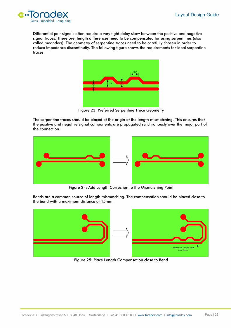
Differential pair signals often require a very tight delay skew between the positive and negative
signal traces. Therefore, length differences need to be compensated for using serpentines (also
called meanders). The geometry of serpentine traces need to be carefully chosen in order to
reduce impedance discontinuity. The following figure shows the requirements for ideal serpentine
traces:
Figure 23: Preferred Serpentine Trace Geometry
The serpentine traces should be placed at the origin of the length mismatching. This ensures that
the positive and negative signal components are propagated synchronously over the major part of
the connection.
Figure 24: Add Length Correction to the Mismatching Point
Bends are a common source of length mismatching. The compensation should be placed close to
the bend with a maximum distance of 15mm.
Figure 25: Place Length Compensation close to Bend
<2S
S
W
<3W
Compensate close to bend (max 15mm)

Layout Design Guide
Toradex AG l Altsagenstrasse 5 l 6048 Horw l Switzerland l +41 41 500 48 00 l www.toradex.com l [email protected] Page | 23
Often two bends compensate each other. If the bends are closer than 15mm, no additional
compensation with serpentines is necessary. The signals should not propagate asynchronously over
a distance greater than 15mm.
Figure 26: Bends can compensate each other
Each segment of a differential pair connection needs to be matched individually. A connection can
be segmented by a connector, serial coupling capacitors or vias. The two bends in the following
figure would compensate each other. Since the vias divide the differential pair into two segments,
the bends need to be compensated individually. This makes sure that the positive and negative
signals are propagated synchronously through the vias. The violation of this rule might need to be
checked manually as the DRC may only check the length difference over the whole connection.
Figure 27: Length Differences need to be compensated in each Segment
The signal speed is not equal for different layers. Since the difference is hard to estimate, it is
preferable to route signals on the same layer if they need to be matched. For example, the LVDS
display interface requires tight matching between the signal pairs and the clock pair. It is
preferable to route all data and clock signals of an LVDS channel on the same layer.
Figure 28: Pairs within same Interface should be routed preferable on same Layer
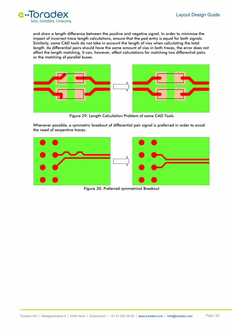
Please be aware that some CAD tools also accounts the trace length inside a pad to its total
length. The following figure shows two layouts which are similar from an electrical point of view.
On the left side, the traces inside the capacitor pads do not have equal length. Even though the
signals are not using the internal traces, some CAD tools use this as part of the length calculation
No compensation needed if distance between two
compensating bends are closer than 15mm
Layout Design Guide
Toradex AG l Altsagenstrasse 5 l 6048 Horw l Switzerland l +41 41 500 48 00 l www.toradex.com l [email protected] Page | 24
and show a length difference between the positive and negative signal. In order to minimize the
impact of incorrect trace length calculations, ensure that the pad entry is equal for both signals.
Similarly, some CAD tools do not take in account the length of vias when calculating the total
length. As differential pairs should have the same amount of vias in both traces, the error does not
affect the length matching. It can, however, affect calculations for matching two differential pairs
or the matching of parallel buses.
Figure 29: Length Calculation Problem of some CAD Tools
Whenever possible, a symmetric breakout of differential pair signal is preferred in order to avoid
the need of serpentine traces.
Figure 30: Preferred symmetrical Breakout

Layout Design Guide
Toradex AG l Altsagenstrasse 5 l 6048 Horw l Switzerland l +41 41 500 48 00 l www.toradex.com l [email protected] Page | 25
If the space between the pads permits, try to add a small loop to the shorter trace. This is the
preferred solution for matching the length difference as opposed to creating a serpentine trace.
Figure 31: Preferred Breakout of Differential Pairs
6.8 Signal Return Path
An incorrect signal return path is one of the most common sources for noise coupling and EMI
problems. The return path of the signal current should always be considered when routing a
signal. Power rails and low speed signals take the shortest (lowest resistance) path for the return
current. In contrast, the return current of high speed signals tries to follow the signal path.
Differential pair signals feature a positive and negative signal trace. Even these signals require a
return path which needs to be considered when routing such signals.
Figure 32: Return Current tries to follow the Signal Path
Source Sink
Reference Plane GND
Source Sink
Reference Plane GND

Layout Design Guide
Toradex AG l Altsagenstrasse 5 l 6048 Horw l Switzerland l +41 41 500 48 00 l www.toradex.com l [email protected] Page | 26
A signal should not be routed over a spit plane as the return path is not able to follow the signal
trace. If a plane is split between a sink and source, route the signal trace around it. If the forward
and return paths of a signal are separated, the area between them acts as a loop antenna.
Figure 33: Avoid Routing over Split Planes
If a signal needs to be routed over two different reference planes, a stitching capacitor between
the two reference planes is needed. The capacitor allows the return current to travel from one
reference plane to the other. The capacitor should be placed close to the signal path in order to
keep the distance between forward and return path small. A good value for the stitching capacitor
is between 10nF and 100nF.
Figure 34: Stitching Capacitor needed when routed over Split Planes
Plane obstructions and plane slots should be avoided in general. Try to avoid routing signals over
such obstructions. If unavoidable, stitching capacitors should be used to minimize the problems
created by a separated return path.
Figure 35: Stitching Capacitor needed when routing over Plane Obstructs
Source Sink
Reference Plane Analogue GND
Source Sink
Reference Plane GND
Reference Plane Analogue GND
Reference Plane GND
Source
Sink
Source
Sink
Reference Plane VCC1
VCC1 VCC2
Reference Plane VCC1
Reference Plane VCC2
Stitching Capacitor
Reference Plane VCC2
Source Sink
Reference Plane GND
PlaneObstruct
Source Sink
Reference Plane GND
PlaneObstruct
Stitching CapacitorGND GND

Layout Design Guide
Toradex AG l Altsagenstrasse 5 l 6048 Horw l Switzerland l +41 41 500 48 00 l www.toradex.com l [email protected] Page | 27
Voids in reference planes can result when placing vias close together. Be aware of such voids when
routing high-speed signals. Try to avoid large void areas by ensuring adequate separation between
vias. Sometimes, it is better to place fewer ground and power vias in order to reduce via voids.
Figure 36: Avoid Via Plane Voids
The return path needs to be considered at the source and sink of a signal. The left figure below
shows a bad example. As there is only one single ground via on the source side, the return current
cannot travel back over the reference ground plane as intended. The return path for the current is
the ground connection on the top layer instead. The problem is that the impedance of the signal
trace is calculated as referenced to the ground plane and not to the ground trace on the top layer.
Therefore, it is necessary to place ground vias at the source and sink side of the signal. This
permits the return current to travel back on the ground plane.
Figure 37: Consider Return Path when placing Ground Vias
When a signal trace uses a power plane as reference, the signal needs to be able to travel back
over the power plane. In the source and sink, the signals are referenced to ground. In order to
change the reference to the power plane, stitching capacitors at the sink and source are needed. If
the sink and source are using the same power rail for their supply, the bypass capacitors can act as
stitching capacitors if they are placed close to the signal entry/exit point. A good value for the
stitching capacitor is between 10nF and 100nF.
Figure 38: Add Stitching Capacitors when using Power Plane as Reference
Source Sink
Reference Plane GND
Source Sink
Reference Plane GND
GND
Out
GND
Out
GND
In
GND
In
GND
GND
Out
GND
Out
GND
In
GND
In
GND
GND
Reference PlaneGND
Reference PlaneGND
Source
Sink
Source
Sink
Reference PlaneVCC
Reference PlaneVCC
VCC
VCC
GND
Stitching Capacitor
Stitching Capacitor
GND

Layout Design Guide
Toradex AG l Altsagenstrasse 5 l 6048 Horw l Switzerland l +41 41 500 48 00 l www.toradex.com l [email protected] Page | 28
If a signal trace switches layer and therefore, also the reference ground plane, stitching vias should
to be added close to the layer change vias. This allows the return current to change ground plane.
For differential signals, switching ground vias should be placed symmetrically.
Figure 39: Place Stitching Vias when Signal changes Ground Reference
If a signal trace switches to a layer which has a different net as reference (e.g. from ground
reference to power plane reference), stitching capacitors are required. This allows the return
current to flow from the ground plane through the stitching capacitor to the power plane. Stitching
capacitor placement and routing should be symmetrical for differential pair signals.
Figure 40: Place Stitching Capacitors when changing Signal Reference Plane
Layer 1
Layer 2
Layer 3
Layer 4
GNDReference for Layer 1
GNDReference for Layer 4
Layer 1
Layer 2
Layer 3
Layer 4
GNDReference for Layer 1
GNDReference for Layer 4
Reference Plane GND (L2)
Reference Plane GND (L3)
Reference Plane GND (L2)
Reference Plane GND (L3)
Reference Plane GND (L2)
Stitching Capacitor
GNDReference for Layer 1
VCCReference for Layer 4
L1
L2
L3
L4
Stitching Capacitor
Stitching Capacitor
Stitching Capacitor
VCC
VCC
GND
GND
GNDReference for Layer 1
VCCReference for Layer 4
L1
L2
L3
L4
Reference Plane VCC (L3)
Reference Plane GND (L2)
Reference Plane VCC (L3)

Layout Design Guide
Toradex AG l Altsagenstrasse 5 l 6048 Horw l Switzerland l +41 41 500 48 00 l www.toradex.com l [email protected] Page | 29
Avoid routing high-speed signals on the edge of reference planes or close to PCB borders.
Otherwise, this can adversely affect the trace impedance.
Figure 41: Do not route High Speed Signals at Plane and PCB borders
6.9 Analogue and Digital Ground
Analogue signals and circuits can be very sensitive to digital noise. There are two main coupling
problems which can introduce digital noise into the analogue part. The first one is the capacitive and inductive coupling of the signals. This coupling can be avoided by separating the signals
from each other. Special care should be taken if analogue and digital signals are routed in parallel
over long distances. Increase the space between such signals as much as possible. Try to keep the
analogue part away from clock signals and high current switching components (e.g. power
supplies).
The second type of coupling is conductive coupling. The left figure shown below explains this
problem. If the digital and analogue share a common return path for the power supply, the current
spikes of the digital circuit can be coupled over the parasitic resistance and inductance to the
analogue supply. The same coupling exists if the return path of signals is common. It is necessary
to separate the return path of the digital circuits from the return path of analogue circuits.
Figure 42: Separate Return Path of Analogue and Digital Supply and Signals
There are two different approaches for the separation of the digital and analogue return path
(ground plane separations). The first physically divides the analogue ground planes from the digital
one, and is referred to as the “Split Plane Approach”. The second divides the grounds virtually, and
is similarly referred to as the “Virtual Split Plane Approach”. Both approaches have their
advantages which make it difficult to judge which one amongst them is better.
Reference Plane GND
Reference Plane GND
VCC Plane VCC Plane
Analogue Cricuit
Digital Cricuit
DigitalSupply
AnalogueSupply
ID
IA
IDIA+ID
Analogue Cricuit
Digital Cricuit
DigitalSupply
AnalogueSupply
ID
IA
ID
IA
Parasitic Resistance andIncuctance of Traces
Parasitic Resistance andIncuctance of Traces
Layout Design Guide
Toradex AG l Altsagenstrasse 5 l 6048 Horw l Switzerland l +41 41 500 48 00 l www.toradex.com l [email protected] Page | 30
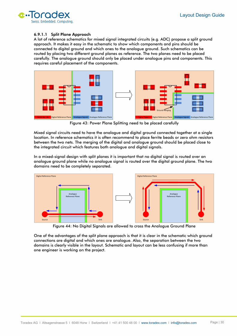
6.9.1.1 Split Plane Approach
A lot of reference schematics for mixed signal integrated circuits (e.g. ADC) propose a split ground
approach. It makes it easy in the schematic to show which components and pins should be
connected to digital ground and which ones to the analogue ground. Such schematics can be
routed by placing two different ground planes as reference. The two planes need to be placed
carefully. The analogue ground should only be placed under analogue pins and components. This
requires careful placement of the components.
Figure 43: Power Plane Splitting need to be placed carefully
Mixed signal circuits need to have the analogue and digital ground connected together at a single
location. In reference schematics it is often recommend to place ferrite beads or zero ohm resistors
between the two nets. The merging of the digital and analogue ground should be placed close to
the integrated circuit which features both analogue and digital signals.
In a mixed-signal design with split planes it is important that no digital signal is routed over an
analogue ground plane while no analogue signal is routed over the digital ground plane. The two
domains need to be completely separated.
Figure 44: No Digital Signals are allowed to cross the Analogue Ground Plane
One of the advantages of the split plane approach is that it is clear in the schematic which ground
connections are digital and which ones are analogue. Also, the separation between the two
domains is clearly visible in the layout. Schematic and layout can be less confusing if more than
one engineer is working on the project.
Digital Signals Analogue SignalsDigital Reference Plane Analogue Reference Plane Digital Signals Analogue SignalsDigital Reference Plane Analogue Reference Plane
Ground Merging
Source Sink Source Sink
Digital Reference Plane
AnalogueReference Plane
Digital Reference Plane
AnalogueReference Plane

Layout Design Guide
Toradex AG l Altsagenstrasse 5 l 6048 Horw l Switzerland l +41 41 500 48 00 l www.toradex.com l [email protected] Page | 31
6.9.1.2 Virtual Split Approach
The virtual split approach does not split the analogue and digital ground in the schematic diagram.
In the layout, the two ground domains are not electrically split. The trick is to implement the layout
as if there is an imaginary separation between the analogue and digital ground. Some CAD tools
allow drawing a help line on an unused mechanical layer. The components need to be placed
carefully on the correct side of the virtual split planes.
Figure 45: Careful Component Placement needed even with Virtual Plane Splitting
The virtual line between the two ground domains needs to be respected during the routing. No
digital or analogue signal trace is permitted to cross the virtual split line. The virtual split line
should not be placed using a very complicated shape as there are no plane obstructs to keep the
analogue and digital return current separated.
Figure 46: No Digital Signals are allowed to cross the Virtual Analogue Ground
Routing can be more challenging with the virtual split plane approach as it is easy to make an
improper separation of the two domains which will not be picked up by the DRC. Special care has
to be taken that the analogue and digital ground parts are correctly split. If the layout is correctly
implemented with this approach, a better solution can be achieved than with the physical split
plane approach.
Digital Signals Analogue Signals Digital and Analogue Reference Plane
Virtual Ground Split
Digital Signals Analogue Signals Digital and Analogue Reference Plane
Source Sink
Analogue Parts
Source Sink
Digital Parts
Virtual Ground Split
Digital and Analogue Reference Plane
Analogue Parts
Digital Parts
Virtual Ground Split
Digital and Analogue Reference Plane
Layout Design Guide
Toradex AG l Altsagenstrasse 5 l 6048 Horw l Switzerland l +41 41 500 48 00 l www.toradex.com l [email protected] Page | 32
7 Layout Requirements of Interfaces
Depending on the type of interface, there are different layout requirements available. This section
provides an overview of the major interfaces that can be found on an Apalis or Colibri module. If
the information is missing for an interface, check the according module datasheet or contact the
Toradex support team.
The differential pair signals normally distinguish between two different length matching
requirements. The first requirement is the maximum intra-pair skew. This is the maximum allowed
length differences between the positive and negative signal of the pairs. As described in section
6.7, not only should the overall length be matched, but also the length within a section of the
signal should be corrected. It is important that the positive and negative signal components are
propagated synchronously. Only if these signals are synchronous, their fields are compensated and
the electromagnetic radiation is reduced.
The second length matching requirement is the maximum allowed skew between the clock and
signal pairs or between different pairs of the same interface. Some of the interfaces (e.g. PCIe,
SATA, and USB3.0) are recovering the clock signal out of the data signals. Therefore, the matching
between the clock and data signals can be quite relaxed (e.g. 240mm). Do not try to overmatch
such interfaces since it is really not required and the additional meander just introduces other
signal quality problems. On the other hand there are interfaces which do not have an embedded
clock signal (e.g. LVDS LCD interface). Please route these signals very carefully. The length
matching between the clock and data signals needs to be met (e.g. 0.5mm).
Vias introduce a major discontinuity of the impedance and can create signal stubs. Therefore, the
amount of vias should be kept as low as possible. Of course, some vias cannot be avoided.
Therefore, some of the interfaces have a budget of maximum amount of vias from in the complete
connection. The following sections show the maximum allowed vias on the carrier board, not in the
complete connection.

Layout Design Guide
Toradex AG l Altsagenstrasse 5 l 6048 Horw l Switzerland l +41 41 500 48 00 l www.toradex.com l [email protected] Page | 33
7.1 PCI Express
The PCIe interface supports the Polarity Inversion. This means the positive and negative signal pins
can be inverted in order to simplify the layout by avoiding crossing of the signals. Some PCIe
devices support additional Lane Reversal for multi-lane interfaces. Since the standard interfaces of
Apalis provide only a single lane PCIe interface, the Lane Reversal feature is not supported in the
Apalis specifications. Some Apalis modules provide additional multi-lane PCIe interface in the type-
specific area. For such modules, Lane Reversal is only applicable if the PCIe device is supporting it.
Parameter Requirement
Max Frequency Gen1: 1.25GHz (2.5GT/s) Gen2: 2.5GHz (5GT/s) Gen3: 4GHz (8GT/s)
Configuration / Device Organization 1 load
Reference Plane GND or PWR (if PWR, add 10nF stitching capacitors between PWR and GND on both sides of the connection for the return current)
Trace Impedance 90Ω ±15% differential; 50Ω ±15% single ended
Max intra-pair skew <1ps ≈150µm
Max trace length skew between clock and data pairs
<1.6ns ≈240mm
Max trace length on carrier board (device-down)
<300mm
Max trace length on carrier board (PCIe slot connector, PCIe Mini card)
<200mm
Minimum pair to pair spacing >500µm
AC coupling capacitors 100nF ±20%, discrete 0402 package preferable
Maximum allowed via 2 vias for TX traces 4 vias for RX traces (device-down) 2 vias for RX traces (PCIe slot connector, PCIe Mini card)
Table 5: PCIe Layout Requirements
7.2 SATA
The SATA interface does not support the Polarity Inversion. This means the positive and negative
signal pins are not allowed to be swapped for layout simplification.
Parameter Requirement
Max Frequency SATA I: 750MHz (1.5GT/s) SATA II: 1.5GHz (3GT/s) SATA III: 3GHz (6GT/s)
Configuration / Device Organization 1 load
Reference Plane GND or PWR (if PWR, add 10nF stitching capacitors between PWR and GND on both sides of the connection for the return current)
Trace Impedance 90Ω ±15% differential; 55Ω ±15% single ended
Max intra-pair skew <1ps ≈150µm
Max trace length skew between data pairs
<0.8ns ≈120mm
Max trace length on carrier board <150mm
Minimum pair to pair spacing >500µm
AC coupling capacitors No coupling capacitors needed on the carrier board
Maximum allowed via 2 vias for RX and TX traces
Table 6: SATA Layout Requirements

Layout Design Guide
Toradex AG l Altsagenstrasse 5 l 6048 Horw l Switzerland l +41 41 500 48 00 l www.toradex.com l [email protected] Page | 34
7.3 Ethernet
The Ethernet MDI signals are analogue differential pair signals which need to be routed carefully.
Try to keep the MDI signals as short as possible and keep them away from digital signals. Try to
avoid any stubs on these signals.
Parameter Requirement
Max Frequency 10Base-T: 10MHz (10Mbit/s) 100Base-TX: 31.25MHz (100Mbit/s) 1000Base-T: 62.5MHz (1Gbit/s)
Configuration / Device Organization 1 load
Reference Plane GND or PWR (if PWR, add 10nF stitching capacitors between PWR and GND on both sides of the connection for the return current)
Trace Impedance 95Ω ±15% differential; 55Ω ±15% single ended
Max intra-pair skew <1.6ps ≈250µm
Max trace length skew between data pairs
<330ps ≈50mm
Max trace length on carrier board between module connector and magnetics
<~100mm, keep it as short as possible
Max trace length on carrier board between magnetics and Ethernet Jack (discrete magnetics)
Place magnetics as close as possible to the Ethernet connector in order to reduce EMC and ESD problems. Separate the reference ground under the traces between magnetics and Ethernet connector. Keep a minimum distance of 2mm between this ground and the common ground.
Minimum pair to pair spacing >450µm
Minimum spacing between MDI signals and other high speed signals
>7.5mm
Minimum spacing between MDI signals and low speed signals
>2.5mm
Maximum allowed via 2 vias for all MDI traces
Table 7: Ethernet Layout Requirements
If discrete magnetics are used instead of a RJ-45 Ethernet jack with integrated magnetics, special
care has to be taken to route the signals between the magnetics and the jack. These signals are
required to be of high voltage and isolated from other signals. It is therefore necessary to place a
dedicated ground plane under these signals which has a minimum separation of 2mm from every
other signal and plane. Additionally, a separate shield ground for the LAN device is needed. Try to
place the magnetics as close as possible to the Ethernet jack. This reduces the length of the signal
traces between the magnetics and jack.
Layout Design Guide
Toradex AG l Altsagenstrasse 5 l 6048 Horw l Switzerland l +41 41 500 48 00 l www.toradex.com l [email protected] Page | 35
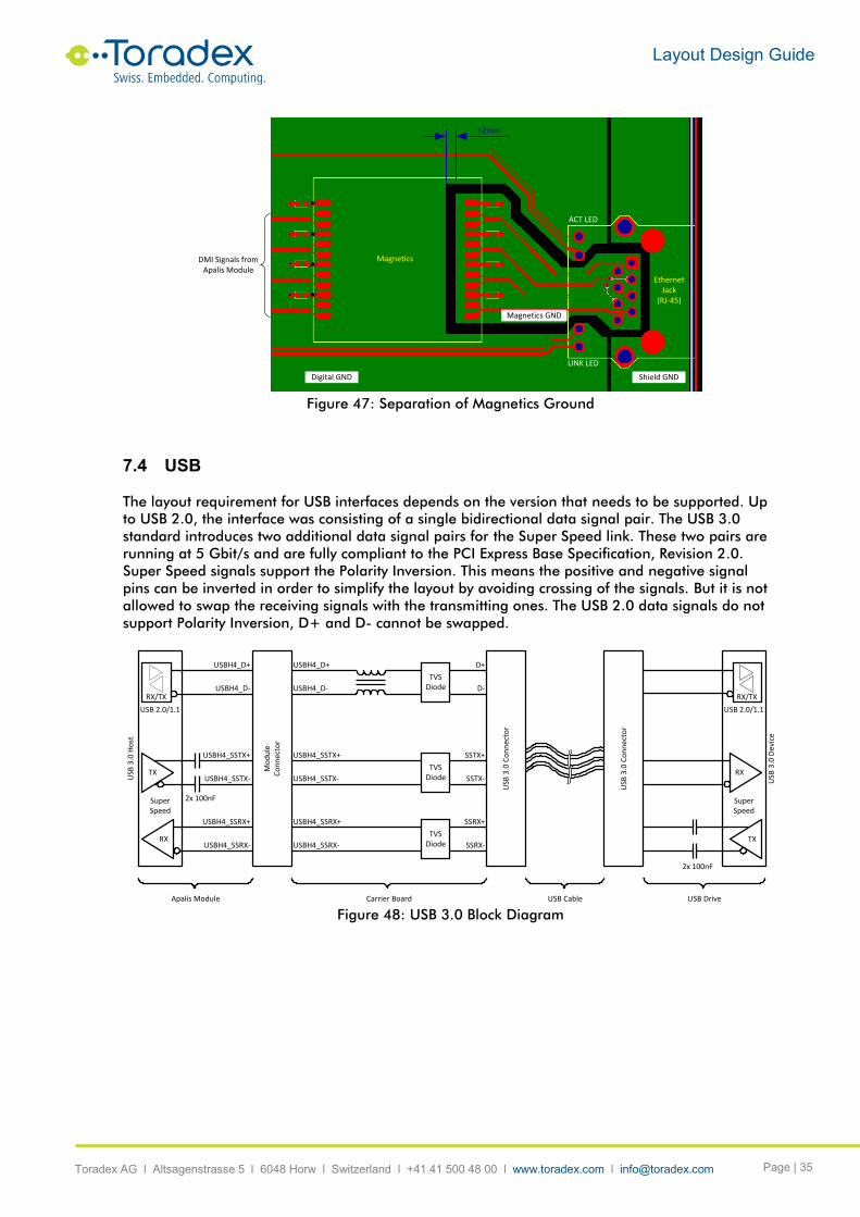
Figure 47: Separation of Magnetics Ground
7.4 USB
The layout requirement for USB interfaces depends on the version that needs to be supported. Up
to USB 2.0, the interface was consisting of a single bidirectional data signal pair. The USB 3.0
standard introduces two additional data signal pairs for the Super Speed link. These two pairs are
running at 5 Gbit/s and are fully compliant to the PCI Express Base Specification, Revision 2.0.
Super Speed signals support the Polarity Inversion. This means the positive and negative signal
pins can be inverted in order to simplify the layout by avoiding crossing of the signals. But it is not
allowed to swap the receiving signals with the transmitting ones. The USB 2.0 data signals do not
support Polarity Inversion, D+ and D- cannot be swapped.
Figure 48: USB 3.0 Block Diagram
Digital GND Shield GND
Magnetics GND
DMI Signals fromApalis Module
Magnetics
EthernetJack
(RJ-45)
LINK LED
ACT LED
>2mm
Apalis Module Carrier Board
TX
RX
RX
TX
USBH4_SSTX+
USBH4_SSTX-
USBH4_SSRX+
USBH4_SSRX-
USBH4_SSTX+
USBH4_SSTX-
USBH4_SSRX+
USBH4_SSRX-
2x 100nF
2x 100nF
SSTX+
SSTX-
SSRX+
SSRX-
USBH4_D+
USBH4_D-
USBH4_D+
USBH4_D-RX/TX
USB
3.0
Ho
st
Super Speed
USB 2.0/1.1
Mo
du
le
Co
nn
ect
or
USB
3.0
Co
nn
ecto
r
D+
D-
USB
3.0
Dev
ice
Super Speed
USB 2.0/1.1
RX/TX
USB
3.0
Co
nn
ecto
r
USB DriveUSB Cable
TVSDiode
TVSDiode
TVSDiode

Layout Design Guide
Toradex AG l Altsagenstrasse 5 l 6048 Horw l Switzerland l +41 41 500 48 00 l www.toradex.com l [email protected] Page | 36
7.4.1.1 USB 2.0 Signals
Parameter Requirement
Max Frequency Low Speed: 750kHz (1.5Mbit/s) Full Speed: 6MHz (12Mbit/s) High Speed 240MHz (480Mbit/s)
Configuration / Device Organization 1 load (10pF High Speed, 150pF Full Speed, 600pF Low Speed)
Reference Plane GND or PWR (if PWR, add 10nF stitching capacitors between PWR and GND on both sides of the connection for the return current)
Trace Impedance 90Ω ±15% differential; 50Ω ±15% single ended
Max intra-pair skew <7.5ps ≈1.1mm
Max trace length on carrier board (USB connector)
<200mm
AC coupling capacitors No coupling capacitors allowed
Maximum allowed via A minimum amount of vias should be used.
Table 8: USB2.0 Layout Requirements
7.4.1.2 USB 3.0 Signals
Parameter Requirement
Max Frequency Super Speed: 2.5GHz (5GT/s)
Configuration / Device Organization 1 load
Reference Plane GND or PWR (if PWR, add 10nF stitching capacitors between PWR and GND on both sides of the connection for the return current)
Trace Impedance 90Ω ±15% differential; 50Ω ±15% single ended
Max intra-pair skew <1ps ≈150µm
Max trace length skew between RX and TX data pairs
<1.6ns ≈240mm
Max trace length on carrier board (USB3.0 connector)
<200mm
Minimum pair to pair spacing <500µm
AC coupling capacitors 100nF ±20%, discrete 0402 package preferable
Maximum allowed via 2 vias for TX traces 4 vias for RX traces (device-down) 2 vias for RX traces (USB3.0 connector)
Table 9: USB3.0 Layout Requirements
Layout Design Guide
Toradex AG l Altsagenstrasse 5 l 6048 Horw l Switzerland l +41 41 500 48 00 l www.toradex.com l [email protected] Page | 37
7.5 Parallel RGB LCD Interface
The layout requirements depend on the pixel clock and therefore on the required display
resolution. The requirements below can be greatly relaxed if lower resolutions such as VGA
640x480 are used. The maximum length restrictions are defined due to electromagnetic radiation
problems associated with the parallel interface. From the timing perspective, the trace length of the
interface is not limited.
Parameter Requirement
Max Frequency Depending on maximum resolution of the module (e.g. 162MHz for VESA 1600x1200@60Hz). Check the datasheet of the Apalis module.
Configuration / Device Organization 1 load (multiple load possible for lower resolutions)
Reference Plane GND or PWR (if PWR, add 10nF stitching capacitors between PWR and GND on both sides of the connection for the return current)
Trace Impedance 50Ω ±15% single ended
Max skew between data signal and clock
<100ps ≈15mm, depends on pixel clock, requirement can be relaxed for lower resolution displays
Max trace length (RGB displays, including flex cable length)
<100mm (long distances only recommended for low resolution displays)
Max trace length (converter on carrier board)
<50mm
Table 10: Parallel RGB LCD Interface Layout Requirements
7.6 LVDS LCD Interface
The LVDS LCD interface does not have the clock embedded in the data signals. Therefore, a proper
length matching between the clock pair and the data signals is essential and depends on the
display resolution.
Parameter Requirement
Max Frequency Depending on maximum resolution of the module. The maximum frequency is 7 times higher than the pixel clock in single channel mode.
Configuration / Device Organization 1 load
Reference Plane GND or PWR (if PWR, add 10nF stitching capacitors between PWR and GND on both sides of the connection for the return current)
Trace Impedance 100Ω ±15% differential; 55Ω ±15% single ended
Max intra-pair skew <1ps ≈150µm
Max trace length skew between clock and data pairs
<3.5ps ≈500µm, depends on LVDS frequency since clock is not embedded, can be relaxed for lower resolutions
Max trace length on carrier board and display cable
<500mm
Minimum pair to pair spacing >2x intra-pair spacing
Maximum allowed via Minimize the number of via in LVDS traces
Table 11: LVDS Layout Requirements
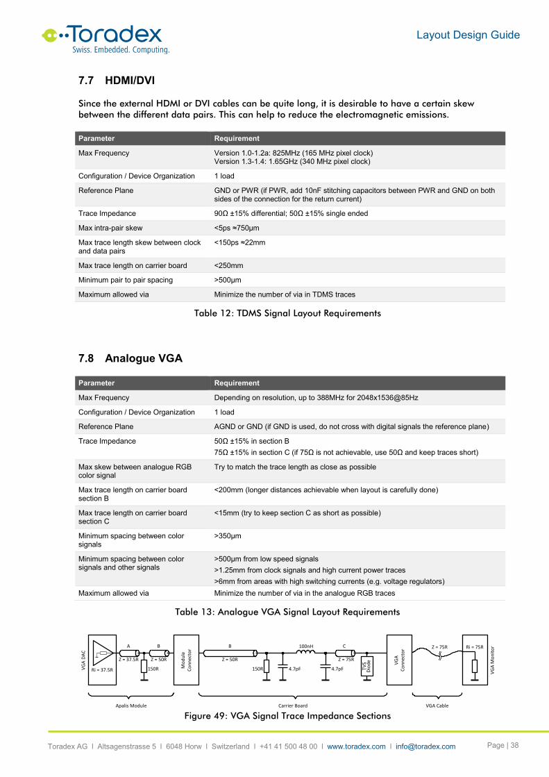
Layout Design Guide
Toradex AG l Altsagenstrasse 5 l 6048 Horw l Switzerland l +41 41 500 48 00 l www.toradex.com l [email protected] Page | 38
7.7 HDMI/DVI
Since the external HDMI or DVI cables can be quite long, it is desirable to have a certain skew
between the different data pairs. This can help to reduce the electromagnetic emissions.
Parameter Requirement
Max Frequency Version 1.0-1.2a: 825MHz (165 MHz pixel clock) Version 1.3-1.4: 1.65GHz (340 MHz pixel clock)
Configuration / Device Organization 1 load
Reference Plane GND or PWR (if PWR, add 10nF stitching capacitors between PWR and GND on both sides of the connection for the return current)
Trace Impedance 90Ω ±15% differential; 50Ω ±15% single ended
Max intra-pair skew <5ps ≈750µm
Max trace length skew between clock and data pairs
<150ps ≈22mm
Max trace length on carrier board <250mm
Minimum pair to pair spacing >500µm
Maximum allowed via Minimize the number of via in TDMS traces
Table 12: TDMS Signal Layout Requirements
7.8 Analogue VGA
Parameter Requirement
Max Frequency Depending on resolution, up to 388MHz for 2048x1536@85Hz
Configuration / Device Organization 1 load
Reference Plane AGND or GND (if GND is used, do not cross with digital signals the reference plane)
Trace Impedance 50Ω ±15% in section B
75Ω ±15% in section C (if 75Ω is not achievable, use 50Ω and keep traces short)
Max skew between analogue RGB color signal
Try to match the trace length as close as possible
Max trace length on carrier board section B
<200mm (longer distances achievable when layout is carefully done)
Max trace length on carrier board section C
<15mm (try to keep section C as short as possible)
Minimum spacing between color signals
>350µm
Minimum spacing between color signals and other signals
>500µm from low speed signals
>1.25mm from clock signals and high current power traces
>6mm from areas with high switching currents (e.g. voltage regulators)
Maximum allowed via Minimize the number of via in the analogue RGB traces
Table 13: Analogue VGA Signal Layout Requirements
Figure 49: VGA Signal Trace Impedance Sections
Apalis Module Carrier Board
VG
A D
AC
Mo
du
le
Co
nn
ecto
r
VG
AC
on
nec
tor
VGA Cable
Z = 37.5R
TVS
Dio
de
VG
A M
on
ito
r
Ri = 37.5R
A B B C100nH Z = 75R
Z = 50R Z = 50R Z = 75R
150R 150R 4.7pF 4.7pF
Ri = 75R

Layout Design Guide
Toradex AG l Altsagenstrasse 5 l 6048 Horw l Switzerland l +41 41 500 48 00 l www.toradex.com l [email protected] Page | 39
7.9 Parallel Camera Interface
The requirements for the layout depends on the pixel clock and therefore on the required camera
resolution and frame rate. The requirements below can be relaxed if lower resolutions such as VGA
640x480@30Hz are used. The maximum length restriction is given due to EMC compliance
problems which otherwise may occur. From the timing perspective, the trace length of the interface
is not limited.
Parameter Requirement
Max Frequency Depending on maximum resolution of the camera and the frame rate.
Configuration / Device Organization 1 source
Reference Plane GND or PWR (if PWR, add 10nF stitching capacitors between PWR and GND on both sides of the connection for the return current)
Trace Impedance 50Ω ±15% single ended
Max skew between data signal and clock
<100ps ≈15mm, depends on pixel clock, requirement can be relaxed for lower resolution displays
Max trace length <50mm
Table 14: Parallel Camera Interface Layout Requirements
7.10 SD/MMC/SDIO
Parameter Requirement
Max Frequency 208MHz (Ultra-High Speed SD, SDR104) 52MHz (MMCplus, eMMC)
Configuration / Device Organization 1 load
Reference Plane GND or PWR (if PWR, add 10nF stitching capacitors between PWR and GND on both sides of the connection for the return current)
Trace Impedance 50Ω ±15% single ended
Max skew between data signal and clock 52MHz MMC
<100ps ≈15mm
Max skew between data signal and clock SDR104
<20ps ≈3mm
Max trace length <100mm
Table 15: SD/MMC/SDIO Layout Requirements

Layout Design Guide
Toradex AG l Altsagenstrasse 5 l 6048 Horw l Switzerland l +41 41 500 48 00 l www.toradex.com l [email protected] Page | 40
7.11 I2C
The I2
C does not need to be routed as differential pair, but it is recommended not to separate data
and clock line too much. It is not required to rout the bus as daisy chain since the stub length is not
a problem. The maximum trace length is limited due to the capacity load of the traces and
attached bus devices. Therefore, try to keep traces as short as possible by using a star topology.
Parameter Requirement
Max Frequency 100kHz (Standard Mode) 400kHz (Fast Mode)
Configuration / Device Organization Multiple load, 400pF (Standard Mode), 100pF (Fast Mode)
Reference Plane GND or PWR (No stitching capacitors required when PWR is used as reference)
Trace Impedance 50Ω ±15% single ended
Max trace length (Standard Mode) <450mm (is mainly limited by the capacitive load)
Max trace length (Fast Mode) <200mm (is mainly limited by the capacitive load)
Table 16: I2
C Layout Requirements
7.12 Display Serial Interface (MIPI/DSI with D-PHY)
Parameter Requirement
Max Frequency 500MHz (1GT/S per data lane)
Configuration/Device Organization 1 load
Reference Plane GND or PWR (if PWR, add 10nF stitching capacitors between PWR and GND on both sides of the connection for the return current)
Trace Impedance 90Ω ±15% differential; 50Ω ±15% single ended
Max Intra-pair Skew <1ps ≈150µm
Max Trace Length Skew between clock and data lanes
<10ps ≈1.5mm
Max Trace Length from Module Connector
200mm
Maximum allowed via Minimize the number of via in each lane
Table 17: DSI Layout Requirements
7.13 Camera Serial Interface (MIPI/CSI-2 with D-PHY)
Parameter Requirement
Max Frequency 500MHz (1GT/S per data lane)
Configuration/Device Organization 1 load
Reference Plane GND or PWR (if PWR, add 10nF stitching capacitors between PWR and GND on both sides of the connection for the return current)
Trace Impedance 90Ω ±15% differential; 50Ω ±15% single ended
Max Intra-pair Skew <1ps ≈150µm
Max Trace Length Skew between clock and data lanes
<10ps ≈1.5mm
Max Trace Length from Module Connector
200mm
Maximum allowed via Minimize the number of via in each lane
Table 18: CSI-2 Layout Requirements

Layout Design Guide
Toradex AG l Altsagenstrasse 5 l 6048 Horw l Switzerland l +41 41 500 48 00 l www.toradex.com l [email protected] Page | 41
DISCLAIMER:
Copyright © Toradex AG. All rights reserved. All data is for information purposes only and not
guaranteed for legal purposes. Information has been carefully checked and is believed to be
accurate; however, no responsibility is assumed for inaccuracies.
Brand and product names are trademarks or registered trademarks of their respective owners.
Specifications are subject to change without notice.