
LATTICE IMAGING IN TRANSMISSION ELECTRON MICROSCOPY … · LATTICE IMAGING IN TRANSMISSION ELECTRON...
14
LATTICE IMAGING IN TRANSMISSION ELECTRON MICROSCOPY Miroslav Karlík Department of Materials, Faculty of Nuclear Sciences and Physical Engineering, Czech Technical University in Prague, Trojanova 13, 120 00 Prague 2, Czech Republic, E-mail: [email protected] Abstract With the resolution becoming sufficient to reveal individ- ual atoms, high-resolution electron microscopy (HREM) can now compete with X-ray and neutron methods to deter- mine quantitatively atomic structures of materials, with the advantage of being applicable to non-periodic objects such as crystal defects. An introduction to the theory and practi- cal aspects of HREM is given. Principles of other lattice imaging techniques in transmission electron microscopy – electron holography and Z-contrast imaging are also de- scribed. Keywords: High-resolution electron microscopy, electron-specimen interactions, electron diffraction, phase contrast, contrast transfer, electron holography, Z-contrast imaging 1. Introduction The last decades are characterized by an evolution from macro- to micro- and more recently to nanotechnology. Ex- amples are numerous, such as nanoparticles, nanotubes, quantum transistors, layered superconducting and mag- netic materials, etc. Since many material properties are strongly connected to the electronic structure, which in turn is considerably dependent on the atomic positions, it is of- ten essential for the materials science to determine atom positions down to a very high precision. Classical X-ray and neutron techniques fail for this task, because of a non-periodic character of nanostructures. Only fast elec- trons are scattered sufficiently strongly with matter to pro- vide local information at the atomic scale. One of the most commonly used high-resolution tech- niques in transmission electron microscopy (TEM) is that of (bright-field) phase-contrast imaging. This relies on the interference between beams scattered by a specimen and is usually performed under parallel beam illumination condi- tions. The main and significant disadvantage of this lattice imaging method is in the difficulty of image interpretation in terms of the atomic structure of the specimen. The inter- pretation is carried out using computer simulations requir- ing input of a specimen structure model, specimen thickness and microscope parameters. Unfortunately, even the best electron microscopes are hampered by the fact that only the intensity (i.e. the square of the amplitude), of the electron wave can be recorded on the photographic film or CCD-camera and an essential part of the electron wave, the phase information, is lost. Holo- graphic recording overcome this problem. The (aberrated) image wave is superimposed with an unscattered plane ref- erence wave resulting in an interference pattern - electron hologram. After acquisition and transfer to a computer sys- tem, amplitude and phase of the electron wave are recon- structed using the laws of Fourier optics by sophisticated image processing. Electron – specimen interaction is then simulated in the same manner as in the case of conventional phase-contrast imaging. On the other hand the Z-contrast technique provides directly interpretable images - maps of scattering power of the specimen. Allowing incoherent imaging of materials, it represents a new approach to high-resolution electron mi- croscopy. The Z-contrast image is obtained by scanning an electron probe of atomic dimensions across the specimen and collecting electrons scattered to high angles. Simulta- neously, spectroscopic techniques can also be used to sup- plement the image, giving information on atomic- resolution chemical analysis and/or local electronic band structure. The resolution of the technique is determined by the size of the electron probe. This paper gives an introduction to the theory and prac- tical aspects of high-resolution electron microscopy. Prin- ciples of electron holography and Z-contrast imaging are also described. 2. Electron – crystal interactions In a transmission electron microscope, a sample in the form of a thin foil is irradiated by electrons having energy of the order of hundreds of keV. In the interior of the crystal the electrons are either undeviated, scattered, or reflected (Fig. 1). Electron scattering may be either elastic or inelastic. In the case of elastic scattering the electrons interact with the electrostatic potential of atomic nuclei. This potential devi- ates the trajectory of incident electrons without any appre- ciable energy loss. In fact a small loss occurs since there is a change in momentum. However, because of the disparity in mass of the scattered electron and the atom the loss is too small (DE/E ~ 10 -9 at aperture angles used in TEM) to affect the coherency of the beam. Ó Krystalografická spoleènost Materials Structure, vol. 8, number 1 (2001) 3 Fig. 1. Interaction of an electron beam with a thin foil
Transcript of LATTICE IMAGING IN TRANSMISSION ELECTRON MICROSCOPY … · LATTICE IMAGING IN TRANSMISSION ELECTRON...
LATTICE IMAGING IN TRANSMISSION ELECTRON MICROSCOPY
Miroslav Karlík
Department of Materials, Faculty of Nuclear Sciences and Physical Engineering, Czech Technical
University in Prague, Trojanova 13, 120 00 Prague 2, Czech Republic,
E-mail: [email protected]
Abstract
With the resolution becoming sufficient to reveal individ-ual atoms, high-resolution electron microscopy (HREM)can now compete with X-ray and neutron methods to deter-mine quantitatively atomic structures of materials, with theadvantage of being applicable to non-periodic objects suchas crystal defects. An introduction to the theory and practi-cal aspects of HREM is given. Principles of other latticeimaging techniques in transmission electron microscopy –electron holography and Z-contrast imaging are also de-scribed.
Keywords:
High-resolution electron microscopy, electron-specimeninteractions, electron diffraction, phase contrast, contrasttransfer, electron holography, Z-contrast imaging
1. Introduction
The last decades are characterized by an evolution frommacro- to micro- and more recently to nanotechnology. Ex-amples are numerous, such as nanoparticles, nanotubes,quantum transistors, layered superconducting and mag-netic materials, etc. Since many material properties arestrongly connected to the electronic structure, which in turnis considerably dependent on the atomic positions, it is of-ten essential for the materials science to determine atompositions down to a very high precision. Classical X-rayand neutron techniques fail for this task, because of anon-periodic character of nanostructures. Only fast elec-trons are scattered sufficiently strongly with matter to pro-vide local information at the atomic scale.
One of the most commonly used high-resolution tech-niques in transmission electron microscopy (TEM) is thatof (bright-field) phase-contrast imaging. This relies on theinterference between beams scattered by a specimen and isusually performed under parallel beam illumination condi-tions. The main and significant disadvantage of this latticeimaging method is in the difficulty of image interpretationin terms of the atomic structure of the specimen. The inter-pretation is carried out using computer simulations requir-ing input of a specimen structure model, specimenthickness and microscope parameters.
Unfortunately, even the best electron microscopes arehampered by the fact that only the intensity (i.e. the squareof the amplitude), of the electron wave can be recorded onthe photographic film or CCD-camera and an essential partof the electron wave, the phase information, is lost. Holo-graphic recording overcome this problem. The (aberrated)image wave is superimposed with an unscattered plane ref-erence wave resulting in an interference pattern - electronhologram. After acquisition and transfer to a computer sys-tem, amplitude and phase of the electron wave are recon-
structed using the laws of Fourier optics by sophisticatedimage processing. Electron – specimen interaction is thensimulated in the same manner as in the case of conventionalphase-contrast imaging.
On the other hand the Z-contrast technique providesdirectly interpretable images - maps of scattering power ofthe specimen. Allowing incoherent imaging of materials, itrepresents a new approach to high-resolution electron mi-croscopy. The Z-contrast image is obtained by scanning anelectron probe of atomic dimensions across the specimenand collecting electrons scattered to high angles. Simulta-neously, spectroscopic techniques can also be used to sup-plement the image, giving information on atomic-resolution chemical analysis and/or local electronic bandstructure. The resolution of the technique is determined bythe size of the electron probe.
This paper gives an introduction to the theory and prac-tical aspects of high-resolution electron microscopy. Prin-ciples of electron holography and Z-contrast imaging arealso described.
2. Electron – crystal interactions
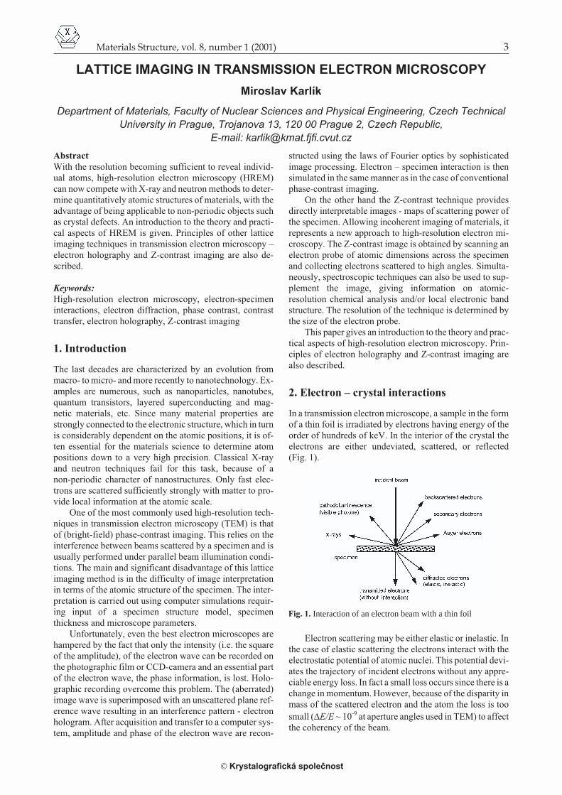
In a transmission electron microscope, a sample in the formof a thin foil is irradiated by electrons having energy of theorder of hundreds of keV. In the interior of the crystal theelectrons are either undeviated, scattered, or reflected(Fig. 1).
Electron scattering may be either elastic or inelastic. Inthe case of elastic scattering the electrons interact with theelectrostatic potential of atomic nuclei. This potential devi-ates the trajectory of incident electrons without any appre-ciable energy loss. In fact a small loss occurs since there is achange in momentum. However, because of the disparity inmass of the scattered electron and the atom the loss is toosmall (�E/E ~ 10-9 at aperture angles used in TEM) to affectthe coherency of the beam.
� Krystalografická spoleènost
Materials Structure, vol. 8, number 1 (2001) 3
Fig. 1. Interaction of an electron beam with a thin foil
� Krystalografická spoleènost
4 M. KARLÍK
In the inelastic case energy of the incident electronmay be transferred to internal degrees of freedom in theatom or specimen in several ways. This transfer may causeexcitation or ionization of the bound electrons, excitationsof free electrons, lattice vibrations and possibly heating orradiation damage of the specimen. The most common in-teractions are those with the electrons in the crystal. In thiscase the energy loss �E is important, because the interact-ing particles have the same mass m. The fraction of energy�E is small as compared to the incident energy E. It is thisprimary process of excitation which is used for the ElectronEnergy Loss Spectrometry (EELS). This kind of spectrom-etry as well as different secondary processes of subsequentdesexcitations of the target – X-ray emission, Auger elec-trons emission, cathodoluminiscence etc. – permit to linkthe structural aspect of the specimen with the informationabout its chemical nature, if the microscope is equippedwith appropriate detectors.
2. 1. Schrödinger equation and the crystalpotential
It seems obvious that the problem of the diffraction of fastelectrons should require the Dirac equation. However, therole of the spin in the interaction is negligible (about onepercent [1,2]) and it is therefore sufficient to use theSchrödinger equation:
��
�
��
�
�
� � � �2
2mV r r E r� ( ) ( ) ( )� �
(1)
where E is the total energy of the electron and V r( )�
its po-tential energy inside the crystal. For fast electrons (E 50keV), it is necessary to take into account the relativistic ef-fects associated with their motion. The solution of theSchrödinger equation in the crystal, where the movingelectron is subjected to the action of a variable potential, isin general very complicated. In case of transmission elec-tron microscopy it is the very high energy of incident elec-trons (~ 105 eV) with respect to the crystal potential (~ 10eV), which enables to simplify the problem. Due to thevery high energy of the incident beam the isotropy of thespace is broken: the majority of electrons propagate in thedirection of the z axis. The space can be divided into the ax-ial direction (z) and two radial directions (x, y). After thisseparation of variables it is possible to modify the equation(1) by introducing:
i) forward (small angle) scattering approximationii) Glauber (projected potential) approximation
The solution of the Schrödinger equation by the multislicemethod is based on these two approximations. Another ap-proach, often used in the TEM for the solution of theSchrödinger equation is the Bloch wave method, intro-duced by Bethe in 1928 [3]. Unfortunately, this method canonly be used for perfect crystals but not for the crystals con-taining grain boundaries, precipitates or other faults. TheBloch waves theory is described in detail in [4].
i) Forward scattering approximation
By introducing the relation between the wave vector�k of
the electron beam and corresponding accelerating potentialE k m �
2 2 2/ to the equation (1) we obtain:
� � � � � ��� k rm
V r r2
2
2� �
�
�
� �( ) (2)
Owing to the high energy of incident electrons it is possibleto consider the action of the crystal potential as a small per-turbation resulting only in a modulation �( )
�r of the primary
electron wave. We are seeking a wave function �( )�r in the
form:� �( ) exp( . ) ( )
� � � �r ik r r (3)
Supposing the expression for the modulation �( )�r , it is pos-
sible to write:
�
�
�
�
�
�
��
��
��
2
2
2
2
2
2 22 2 2
2
x y zik
xik
yik
z
mV rx y z� � � � � �
�
�( ) .
. ( )
�
��
�
�
��r 0
In this equation the term� �
�
��
�
2
22
( ) ( )� �r
zik
r
zz�� may be
neglected since the derivative��
�
( )�r
zchanges only slowly
with z. In other words it is possible to neglect backscatteredelectrons. The equation (1) thus acquires the form of theforward scattering approximation:
��
��
�
�
�
��
��
( )( )
�
�
�r
z
i
k x yik
xik
y
mV r
z
x y � � � �2
2 222
2
2
2 2
�
��
�
� �( )
�r
Two terms in the square brackets may be considered as in-dependent. The first term:
Ax y
ikx
iky
x y � � ��
�
�
�
��
��
2
2
2
22 2
represents the propagation of the electron wave, while thesecond one represents the action of the crystal potential.Therefore:
��
��
( )( ) ( )
�
�
� �r
z
i
kA
mV r r
z
��
���
�2
22
(4)
The physical meaning of these two terms becomes obviousfrom the following: if in the equation (4) we neglect theterm V r( )
�and if we put kx = ky = 0 and k = kz (projection
of k to the directions x a y is very small), we obtain:
��
�
� �
�
� �
�
( ) ( ) ( )� � �r
z
i
k
r
x
i
k
r
y �
2 2
2
2
2
2(5)
This is a 2D equation of heat conduction. Its solution in thepoint (x, y,z) has a form:
��
( , , ) exp ( )x y zk
z
ik
zx y ��
��
�
��
4 22 2
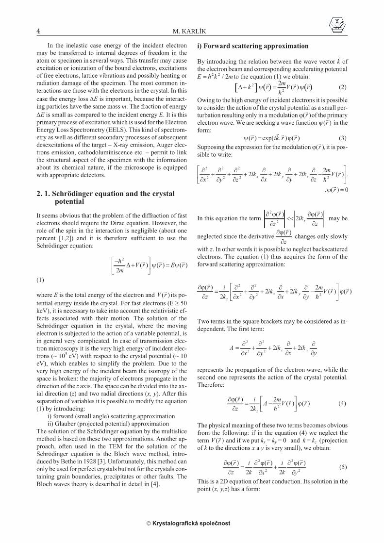
In Fig. 2 A and B there are two point sources of the waves(Huyghens principle) at the level of the plane 1. To find theresult of the interference in the point A' at the level of theplane 2 in the distance z, it is necessary to integrate contri-butions of A, B and all other point sources in the plane 1,represented by the function �( , , )X Y 0 . Thus we obtain anexpression:
� �
�
��
( , , )
( , , )exp ( ) ( )
x y z
k
zX Y
ik
zx X y Y d
� � ��
���
��40
22 2 XdY�
having the form of the convolution integral. Then it is pos-sible to write:
� ��
( , , ) ( , , ) exp ( )x y z X Yk
z
ik
zx y � ��
���
���
!"#
04 2
2 2 (6)
where the term in the complex brackets is the Fresnel prop-agator, describing the propagation of the waves from theplane 1. The result of their interference in the plane 2 isgiven by the convolution.
ii) Glauber aproximation
Neglecting the term A, equation (4) simplifies to the ex-pression:
��
��
( )( ) ( )
�
�
� �r
z
i
k
mV r r
z
�2
22
(7)
from where we obtain (k kz $ ):
��
��
( )( ) ( )
�
�
� �r
z
i
k
mV r r �
2
22
and after integration
ln( )
( )( ) ( , )
��
� % %
�
��
�
�
r
r
iV r dz
iV xy z dz
z z
0 0 0
� �� �
where the constant before the integral was derived from thede Broglie relation & % h m/ (% is the velocity of elec-trons) and relation k 2� &/ . For �( )
�r we obtain Glauber
approximation [5]:
� �%
� '( ) exp ( , ) exp( )�
�r
iV xy z dz i
z
��
��
�
� �0
0
0 (8)
and taking �0 = 1 before the interaction of electrons withthe crystal, the original expression (3) becomes:
� '�( ) exp( )[exp( ]� � �r ik r i$ (
from which it follows that action of the crystal potential re-sults in a phase shift of the incident electron wave. As thepotential energy of electron in the interior of the crystal isnegative, the sign of the phase shift is positive.
2. 2. Multislice method
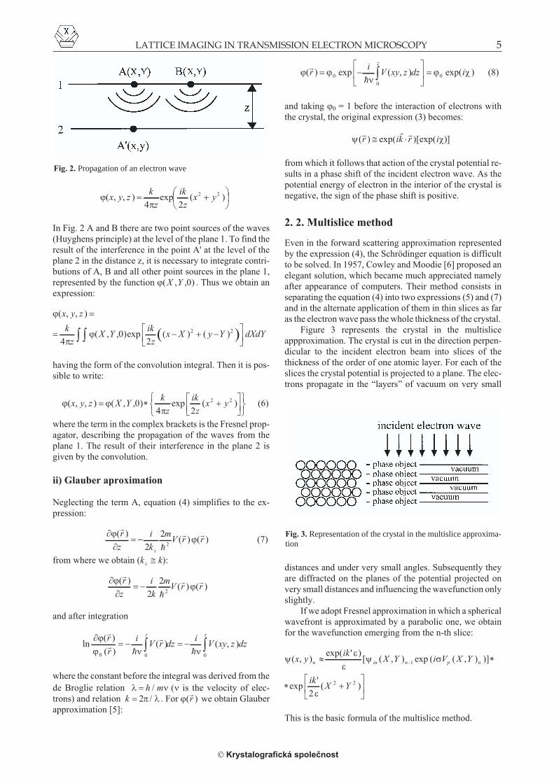
Even in the forward scattering approximation representedby the expression (4), the Schrödinger equation is difficultto be solved. In 1957, Cowley and Moodie [6] proposed anelegant solution, which became much appreciated namelyafter appearance of computers. Their method consists inseparating the equation (4) into two expressions (5) and (7)and in the alternate application of them in thin slices as faras the electron wave pass the whole thickness of the crystal.
Figure 3 represents the crystal in the multisliceappproximation. The crystal is cut in the direction perpen-dicular to the incident electron beam into slices of thethickness of the order of one atomic layer. For each of theslices the crystal potential is projected to a plane. The elec-trons propagate in the “layers” of vacuum on very small
distances and under very small angles. Subsequently theyare diffracted on the planes of the potential projected onvery small distances and influencing the wavefunction onlyslightly.
If we adopt Fresnel approximation in which a sphericalwavefront is approximated by a parabolic one, we obtainfor the wavefunction emerging from the n-th slice:
�)
)�� *( , )
exp( ' )( , ) exp ( ( , ) )]
ex
x yik
X Y i V X Yn in n p n+ �
�
�1
p'( )
ikX Y
22 2
)�
�
��
�
�
This is the basic formula of the multislice method.
� Krystalografická spoleènost
LATTICE IMAGING IN TRANSMISSION ELECTRON MICROSCOPY 5
Fig. 2. Propagation of an electron wave
Fig. 3. Representation of the crystal in the multislice approxima-tion
During calculation of the wavefunction two effects al-ternate. Firstly the phase of the incident electron wave atthe entrance to the given slice is shifted due to the action ofthe projected potential. The phase shift is given by the inte-gral over the thickness ). Subsequent convolution repre-sents the propagation of the wave in a slice of the vacuumof the same thickness ). If ) tends to zero, the result of themultislice simulation tends to the exact solution of theSchrödinger equation. As we are dealing with the slices ofthe finite thickness, it is necessary to determine the largestthickness for which the solution of the Schrödinger equa-tion is still acceptable. Ishizuka and Uyeda [7] give the fol-lowing condition: ) , kd 2 , where k is the wave vector of theelectrons and d is the distance on which the potential doesnot change significantly. As follows from this equation, ifk is of the order of 2.5 1012 m-1 and d ~ 10-11 m, � should belower or equal to 2,5 Å! In fact this condition is strongerthan shows the practice.
The chart of the simulation corresponding to the EMScode written by Stadelmann [8] is shown in Fig. 4. The in-cident wave is firstly multiplied by the phase grating, repre-senting the action of the projected potential Vp(x,y).Subsequently a fast Fourier transform (FFT) of this productis performed, in order to calculate easily the product of con-
volution (multiplication in the Fourier space) with the Fres-nel propagator. After the inverse FFT the calculation eithercontinues or ends and we obtain a wavefunction for a giventhickness of the crystal.
3. Formation and transfer of the contrast byTEM
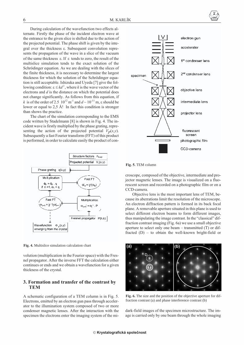
A schematic configuration of a TEM column is in Fig. 5.Electrons, emitted by an electron gun pass through acceler-ator to the illumination system composed of two or morecondenser magnetic lenses. After the interaction with thespecimen the electrons enter the imaging system of the mi-
croscope, composed of the objective, intermediate and pro-jector magnetic lenses. The image is visualized on a fluo-rescent screen and recorded on a photographic film or on aCCD-camera.
Objective lens is the most important lens of TEM, be-cause its aberrations limit the resolution of the microscope.An electron diffraction pattern is formed in its back focalplane. A removable aperture situated in this plane is used toselect different electron beams to form different images,thus manipulating the image contrast. In the “classical” dif-fraction contrast imaging (Fig. 6a) we use a small objectiveaperture to select only one beam – transmitted (T) or dif-fracted (D) – to obtain the well-known bright-field or
dark-field images of the specimen microstructure. The im-age is carried only by one beam through the whole imaging
� Krystalografická spoleènost
6 M. KARLÍK
Fig. 4. Multislice simulation calculation chart
Fig. 5. TEM column
Fig. 6. The size and the position of the objective aperture for dif-fraction contrast (a) and phase interference contrast (b)
system of the microscope. On the other hand phase-contrast lattice imaging relies on the interference betweenthe transmitted and several diffracted beams and so we usea much larger objective aperture (Fig. 6b).
3.1. Transfer of the contrast by the optical system
In order to understand the relation between the wave-function at the exit face of the crystal and its image, it isnecessary to remind the basic principles of the image for-mation under coherent illumination [9-11].
Impulse response and transfer function
A system S assigns to the object defined by a function E r( )�
an image I r S E r( ' ) ( ( ))� �
. If the system is linear, it is possi-ble to decompose the object E r( )
�to a sum of elementary
contributions e ri ( )�
E r c e ri i( ) ( )� �
-having a weight ci and to leave the system to act on each ofthese elements separately. The image I r( ' )
�of the object is
then given by a sum of images of the elementary contribu-tions S e ri( ( ))
�:
I r S E r c S e ri i
i
( ' ) ( ( )) ( ( ))� � �
-If the function entering to the system is an elementary im-pulse (Dirac function .), we obtain:
E r E r r r dr( ) ( ) ( )� � � � �
��/
/
� 1 1 1. , and
I r S E r E r r r dr E r h r( ' ) ( ( )) ( ) ( ) ( ) (� � � � � � � �
� �/
/
� 1 1 1 1. ' , )� �r dr1 1
�/
/
�
where h r r( ' , )� �
1 , the image of the point .( )� �r r� 1 , is the im-
pulse response function.In consequence a linear optical system is fully charac-
terized by point sources in the object plane and by the im-pulse response function, which describes how the image ofany point is influenced by the system. Furthermore, if thesystem is invariant in the space (isoplanar), its impulse re-sponse function h r r( ' , )
� �1 depends only on distances ( ' )
� �r r� 1 .
In other words, the image of a point source (impulse re-sponse to the Dirac function . ) change only its position anddoes not change either its shape or its intensity, if this pointis moved in the object plane. Then it is possible to puth r r( ' , )
� �1 = h( ' )
� �r r� 1 and simplify the preceding expression,
which takes the form of a convolution integral:
I r E r h r r E r h r( ' ) ( ) ( ' ) ( ) ( ' )� � � � � �
� ��/
/
� 1 1 (9)
If we apply a Fourier transform on this expression, we ob-tain a simple equation which links the spectra
~( )I q�
and~
( )E q�
of the image I r( ' )�
and object E r( )�
:
~( )
~( )
~( )I q E q h q
� � � (
Fourier transform of the impulse response function in thisequation,
~( ) ( )exp( ) ( )h q h r iqr dr T q� � �� � �
�/
/
� (10)
is the transfer function of the system which acts in the do-main of spatial frequencies
�q .
Scherzer theory [12] permits to describe the transmis-sion electron microscope as a linear, space invariant systemwithout noise, which is characterized by a transfer func-tion:
T q z i q z q z i q z( , ) exp( ( , )) cos ( , ) sin ( , )� � � � �' ' '� � �
(11)
where �z is the defocus of the objective lens. The real termdescribes the transfer of the amplitude, while the imaginaryterm describes the transfer of the phase contrast (this termis often abbreviated as CTF: "Contrast Transfer Function").Here '( , )
�q z� represents the phase shift of the wave as a
function of the defocus �z and the spatial frequency�q. Spa-
tial frequency in the argument of the transfer function is of-ten replaced by the angle of deviation from the optical axis,which is linked with the spatial frequency by the relation:0 & | |
�q , where 0 0 2 Bragg .
3. 2. Image forming by a lens without aberrations
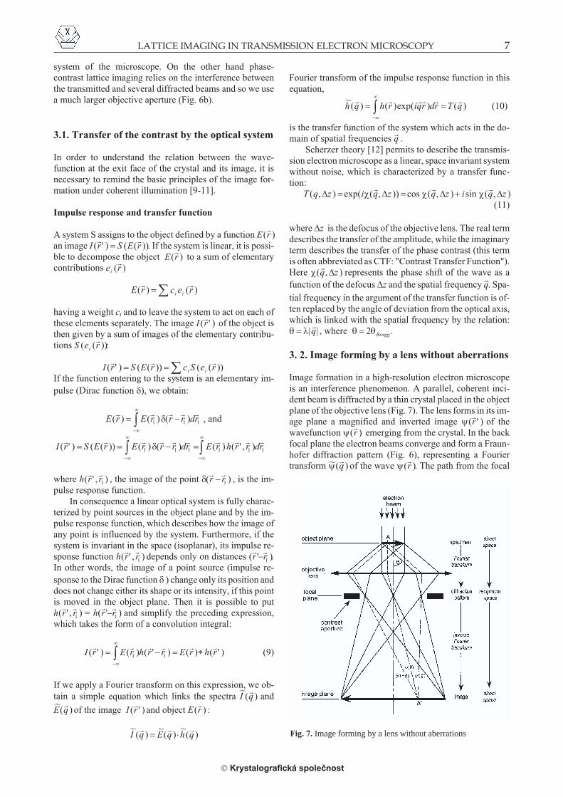
Image formation in a high-resolution electron microscopeis an interference phenomenon. A parallel, coherent inci-dent beam is diffracted by a thin crystal placed in the objectplane of the objective lens (Fig. 7). The lens forms in its im-age plane a magnified and inverted image �( ' )
�r of the
wavefunction �( )�r emerging from the crystal. In the back
focal plane the electron beams converge and form a Fraun-hofer diffraction pattern (Fig. 6), representing a Fouriertransform ~( )�
�q of the wave �( )
�r . The path from the focal
� Krystalografická spoleènost
LATTICE IMAGING IN TRANSMISSION ELECTRON MICROSCOPY 7
Fig. 7. Image forming by a lens without aberrations
plane to the image plane may be described as an inverseFourier transform. Thus, for the overall relation betweenthe object and the image we obtain:
� � �( ' ) {~( )} { { ( )}}� � �r q r F F F
-1 -1 (12)
As the illumination of the object is coherent, the image A'of each of the points A results from an interference of sev-eral (spherical) waves admitted by the opening of the con-trast aperture (Fig. 6b).
The effect of aberrations intervenes at the level of thefocal plane through the action of the transfer function of themicroscope T q z( , )
�� (11). The relation (16) takes a more
precise form:
� �( ' ) { ( ) ( , ) { ( )}}� � � �r D q T q z r ( (F F
-1 � (13)
Where D q( )�
is an aperture function (equal to unity in theopening of the aperture and zero in the rest of the plane),which describes the limitations due to the insertion of theobjective aperture [13, 14].
3. 3. Real lenses and their aberrations
The aberrations of real lenses deform the electron wavesand decrease the resolution of the microscope. Fortunately,in the transmission electron microscopy the electron beamspropagate close to the optical axis and under small angles.Thus we can neglect higher order aberrations, common inthe photon optics. Nevertheless we have to take into ac-count these “axial” aberrations: defocus, spherical aberra-tion, chromatic aberration, astigmatism and coma. The lasttwo aberrations – astigmatism and coma - can be corrected.
3. 3. 1. Spherical aberration
The effect of the spherical aberration (defined by a spheri-cal aberration constant Cs) is to draw the marginal elec-trons (electrons more distant from the optical axis) more tothe optical axis than other ones. Consequently the phaseshift of the beams propagating under a different angle �
with respect to the optical axis is given [12] by:
' 0�&
01
42
4( ) � Cs (14)
3. 3. 2. Defocus
The focal distance of the electron lenses depends on the ex-citation current. The variation of the focal distance resultsin another phase shift
' 0�&
02
22
2( , )� �z z � (15)
which can in certain manner compensate the phase shiftdue to the spherical aberration, if �z is negative (lower cur-rent = weaker lens).
3. 3. 3. Coherent transfer function
If we consider illumination conditions as perfectly coher-ent, the incident beam is:
- monochromatic (temporal coherence) and- parallel (spatial coherence)
there are both phase shifts ' 01( , )�z (14) and ' 02 ( , )�z
(15) in the argument of the coherent transfer function Tc:
T z i C zc s( , ) exp ( ) exp0 ' '�&
0 0� � � �
�
���
�
���
��
!1 2
4 22
4 2"#
(16)
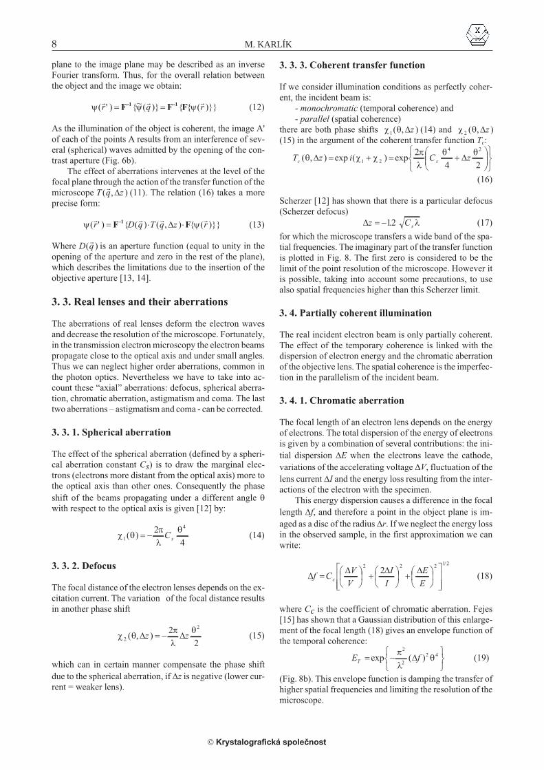
Scherzer [12] has shown that there is a particular defocus(Scherzer defocus)
�z Cs �12. & (17)
for which the microscope transfers a wide band of the spa-tial frequencies. The imaginary part of the transfer functionis plotted in Fig. 8. The first zero is considered to be thelimit of the point resolution of the microscope. However itis possible, taking into account some precautions, to usealso spatial frequencies higher than this Scherzer limit.
3. 4. Partially coherent illumination
The real incident electron beam is only partially coherent.The effect of the temporary coherence is linked with thedispersion of electron energy and the chromatic aberrationof the objective lens. The spatial coherence is the imperfec-tion in the parallelism of the incident beam.
3. 4. 1. Chromatic aberration
The focal length of an electron lens depends on the energyof electrons. The total dispersion of the energy of electronsis given by a combination of several contributions: the ini-tial dispersion �E when the electrons leave the cathode,variations of the accelerating voltage �V, fluctuation of thelens current �I and the energy loss resulting from the inter-actions of the electron with the specimen.
This energy dispersion causes a difference in the focallength �f, and therefore a point in the object plane is im-aged as a disc of the radius �r. If we neglect the energy lossin the observed sample, in the first approximation we canwrite:
�� � �
f CV
V
I
I
E
Ec �
��
�
�� ��
��
�
�� ��
��
�
��
�
���
�
�
2 2 2 1 2
2/
(18)
where Cc is the coefficient of chromatic aberration. Fejes[15] has shown that a Gaussian distribution of this enlarge-ment of the focal length (18) gives an envelope function ofthe temporal coherence:
E fT ���
!"#
exp ( )�
&0
2
2
2 4� (19)
(Fig. 8b). This envelope function is damping the transfer ofhigher spatial frequencies and limiting the resolution of themicroscope.
� Krystalografická spoleènost
8 M. KARLÍK
3. 4. 2. Convergence of the incident beam
The convergence of the incident beam (spatial coherence)limits the resolution of the microscope in a similar manneras the chromatic aberration does [16]. The envelope func-tion of the spatial coherence 1 for a semi-angle of conver-gence is given by the expression:
EJ x
xS
2 1( )(20)
where J1(x) is the Bessel function of the first order and thefirst kind, and x is given by :
� �x z C i fs � ���
!"#
2 23
2�1
0&
& �0
&� �( ) (21)
The spatial coherence envelope is plotted in Fig. 8c.
3. 4. 3. Real transfer function
Real transfer function is given by the product of the expres-sions (16) (19) and (20):
T T E ER C T S ( ( (22)
Its imaginary part is plotted in Fig. 8d. The parameters: Cs
= 0.5 mm, �f = 10 nm and 1 = 1 mrad correspond to the mi-croscope Philips CM20 UltraTwin with a thermoemissionLaB6 gun.
3. 4. 4. Amplitude and intensity transfer
Let us consider a wavefunction � E r( )�
at the exit of thecrystal and its Fourier transform ~ ( )� E q
�. The influence of
the microscope is given by the transfer function:
~ ( ) ( , )� E q T q z� �
� .
In order to obtain the amplitude of the image � IM r( ' )�
, it isnecessary to perform an inverse Fourier transform:
2 3� �IM Er q T q z( ' ) ~ ( ) ( , )� � �
(�F
1 �
Owing to the fact that Fourier transform of a product is aconvolution of Fourier transforms of individual functions,it is possible to write (using the relationF
� 1{ ( , )} ( ' )T q z h r� �� ):
� �IM Er r h r( ' ) ( ) ( ' )� � �
� � (23)
It is the same linear relation as the expression (9), andtherefore the amplitude transfer by the microscope is lin-
ear. However, since the quantity that we detect on the pho-tographic film or on a camera is intensity, we have to studythe intensity transfer.
The intensity of the wave emerging from the crystal isI r rE E( ) | ( )|
� � � 2 , the intensity of its image I rIM ( ' )
�can be
expressed with the aid of the relation (23):
I r r r h rIM IM E( ' ) | ( ' )| | ( ) ( ' )|� � � �
� �� �2 2
Since the functions � E r( )�
and h r( ' )�
are generally com-plex, the relation between the intensity of the object I rE ( )
�
and the intensity of the image I rIM ( ' )�
is not simple.The intensity transfer under the coherent illumination
is not linear. The relation between the object and its imagecan be established only by the calculation.
However, in special cases the non-linearity of thetransfer in intensity is overbalanced by the nature of the ob-ject. This is true for isolated atoms or "weak phase objects"- objects of several nanometers thick only [17]. For a de-tailed analysis of these special cases see [13, 17-19].
If the imaging is incoherent, we obtain an expressionI r I r h rIM E( ' ) ( ) | ( ' )|
� � � � 2which is similar to (23). Therefore
the intensity transfer in this case is linear and thus theZ-contrast imaging gives directly interpretable images (see§ 8).
4. Interpretation of the interference image
The interpretation of interference images with an atomicresolution consists in the exact determination of the posi-tions of atomic columns with respect to the black and whitecontrast on the micrograph. A direct interpretation is possi-ble only in very special cases of "weak-phase objects",where the final image corresponds to the projected poten-tial of the whole specimen.
Real crystals are "strong-phase objects". Neither theirinteraction with the incident electron beam, nor the transferof the intensity of the image are linear. It is not possible to
� Krystalografická spoleènost
LATTICE IMAGING IN TRANSMISSION ELECTRON MICROSCOPY 9
Fig. 8. Contrast transfer function and its envelopes (Scherzerdefocus) for a 200 kV microscope with LaB6 gun, Cs = 0.5 mm.(a) contrast transfer function, (b) spatial coherence envelope, (c)temporal coherence envelope, (d) product (a)*(b)*(c) – amplitudetransfer function, (e) intensity transfer function with the positionsof spatial frequencies corresponding to hkl planes of aluminium.
assign intuitively a crystal structure that diffracted the elec-trons to an experimental image.
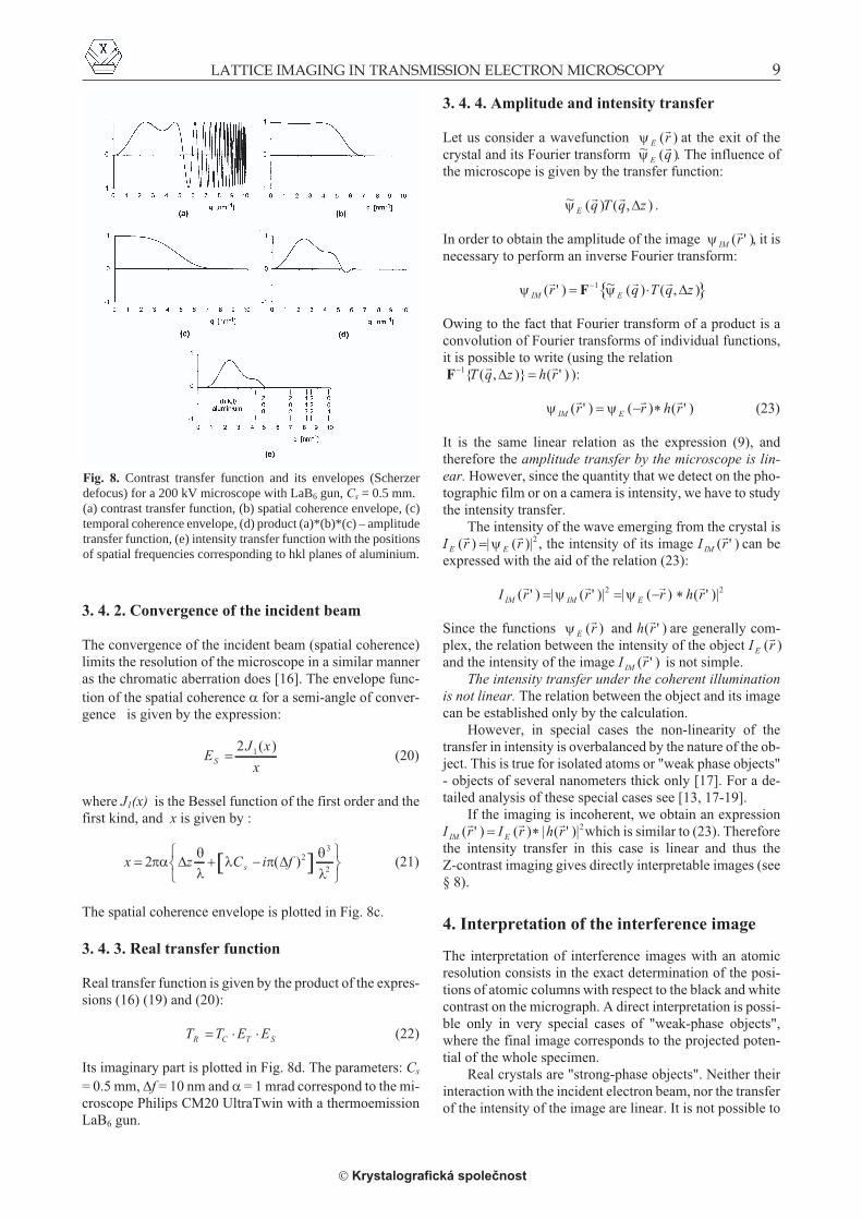
The main problem is that the positions of maxima andminima of interference with respect to atomic columns de-pend at the same time on the crystal thickness and on thedefocus of the objective lens. Furthermore, it is often verydifficult to determine the values of both these experimentalparameters. Fig. 9 shows distribution of minima and max-ima of interference with respect to the positions of atomiccolumns for a wave emerging from a perfect crystal. Inde-pendently on the transfer of the contrast by the microscope,the maxima are placed at the position of atomic columns(z1) or at the "tunnels" between them (z3). However thereare certain thicknesses (z2) for which the emerging wavehas an intermediate form and another series of "supplemen-tary" maxima appears. These three forms of the waves re-peat periodically with the crystal thickness.
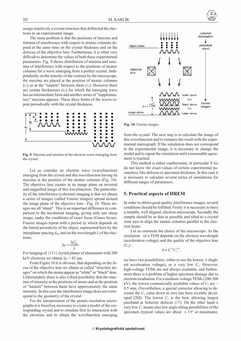
Let us consider an electron wave (wavefunction)emerging from the crystal and this wavefunction having itsmaxima at the position of the atomic columns (Fig. 10).The objective lens creates in its image plane an invertedand magnified image of this wavefunction. The particular-ity of the interference (coherent) imaging is that we obtaina series of images (called Fourier images) spread aroundthe image plane of the objective lens - Fig. 10. These im-ages are all "sharp". This is an important difference in com-parison to the incoherent imaging, giving only one sharpimage, under the conditions of exact focus (Gauss focus).Fourier images repeat with a period �z which depends onthe lateral periodicity of the object, represented here by theinterplanar spacing dhkl and on the wavelength & of the elec-trons:
�zd hkl
2 2
&For imaging of {111} crystal planes of aluminium with 200keV electrons we obtain �z = 43 nm.
From Figure 10 it is obvious, that depending on the fo-cus of the objective lens we obtain so called "structure im-ages" on which the atoms appear as "white" or "black" dots.Unfortunately there is also a third possibility that the max-ima of intensity at the positions of atoms and at the positionof "tunnels" between them have approximately the sameintensity. In this case the interference image does not corre-spond to the geometry of the crystal.
For the interpretation of the atomic resolution micro-graphs it is therefore necessary to create a model of the cor-responding crystal and to simulate first its interaction withthe electrons and to obtain the wavefunction emerging
from the crystal. The next step is to calculate the image ofthis wavefunction and to compare the result with the exper-imental micrograph. If the simulation does not correspondto the experimental image, it is necessary to change themodel and to repeat the simulation until a reasonable agree-ment is reached.
This method is rather cumbersome, in particular if wedo not know the exact values of certain experimental pa-rameters, like defocus or specimen thickness. In this case itis necessary to calculate several series of simulations fordifferent ranges of parameters.
5. Practical aspects of HREM
In order to obtain good quality interference images, severalconditions should be fulfilled. Firstly it is necessary to havea suitable, well aligned, electron microscope. Secondly thesample should be as thin as possible and tilted to a crystalzone axis to align the atomic columns parallel to the elec-tron beam.
Let us comment the choice of the microscope. As theresolution of a TEM depends on the electron wavelength(acceleration voltage) and the quality of the objective lens(Cs) :
. &+ 3 4 1 4/ /Cs ,
we have two possibilities: either to use the lowest & (high-est acceleration voltage), or a very low Cs. However,high-voltage TEMs are not always available, and further-more there is a problem of higher specimen damage due toelectron irradiation. For a medium-voltage TEMs (200-300kV), the lowest commercially available values of Cs are ~0.5 mm. (Nevertheless, a special corrector allowing to de-crease the Cs value down to zero has been recently devel-oped [20]). The lowest Cs is the best, allowing largestpassband at Scherzer defocus (17). On the other hand avery low Cs means also low angle tilting possibilities of thespecimen (typical values are about ± 15° at maximum).
� Krystalografická spoleènost
10 M. KARLÍK
Fig. 9. Maxima and minima of the electron wave emerging fromthe crystal
Fig. 10. Fourier images
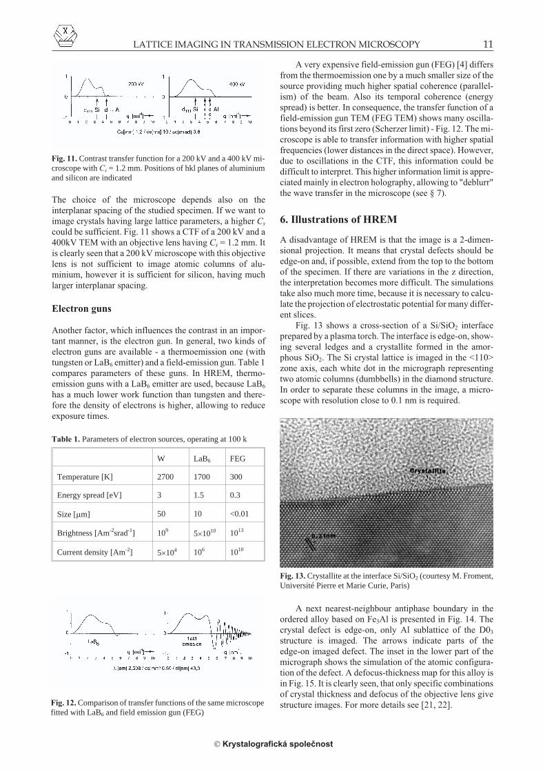
The choice of the microscope depends also on theinterplanar spacing of the studied specimen. If we want toimage crystals having large lattice parameters, a higher Cs
could be sufficient. Fig. 11 shows a CTF of a 200 kV and a400kV TEM with an objective lens having Cs = 1.2 mm. Itis clearly seen that a 200 kV microscope with this objectivelens is not sufficient to image atomic columns of alu-minium, however it is sufficient for silicon, having muchlarger interplanar spacing.
Electron guns
Another factor, which influences the contrast in an impor-tant manner, is the electron gun. In general, two kinds ofelectron guns are available - a thermoemission one (withtungsten or LaB6 emitter) and a field-emission gun. Table 1compares parameters of these guns. In HREM, thermo-emission guns with a LaB6 emitter are used, because LaB6
has a much lower work function than tungsten and there-fore the density of electrons is higher, allowing to reduceexposure times.
A very expensive field-emission gun (FEG) [4] differsfrom the thermoemission one by a much smaller size of thesource providing much higher spatial coherence (parallel-ism) of the beam. Also its temporal coherence (energyspread) is better. In consequence, the transfer function of afield-emission gun TEM (FEG TEM) shows many oscilla-tions beyond its first zero (Scherzer limit) - Fig. 12. The mi-croscope is able to transfer information with higher spatialfrequencies (lower distances in the direct space). However,due to oscillations in the CTF, this information could bedifficult to interpret. This higher information limit is appre-ciated mainly in electron holography, allowing to "deblurr"the wave transfer in the microscope (see § 7).
6. Illustrations of HREM
A disadvantage of HREM is that the image is a 2-dimen-sional projection. It means that crystal defects should beedge-on and, if possible, extend from the top to the bottomof the specimen. If there are variations in the z direction,the interpretation becomes more difficult. The simulationstake also much more time, because it is necessary to calcu-late the projection of electrostatic potential for many differ-ent slices.
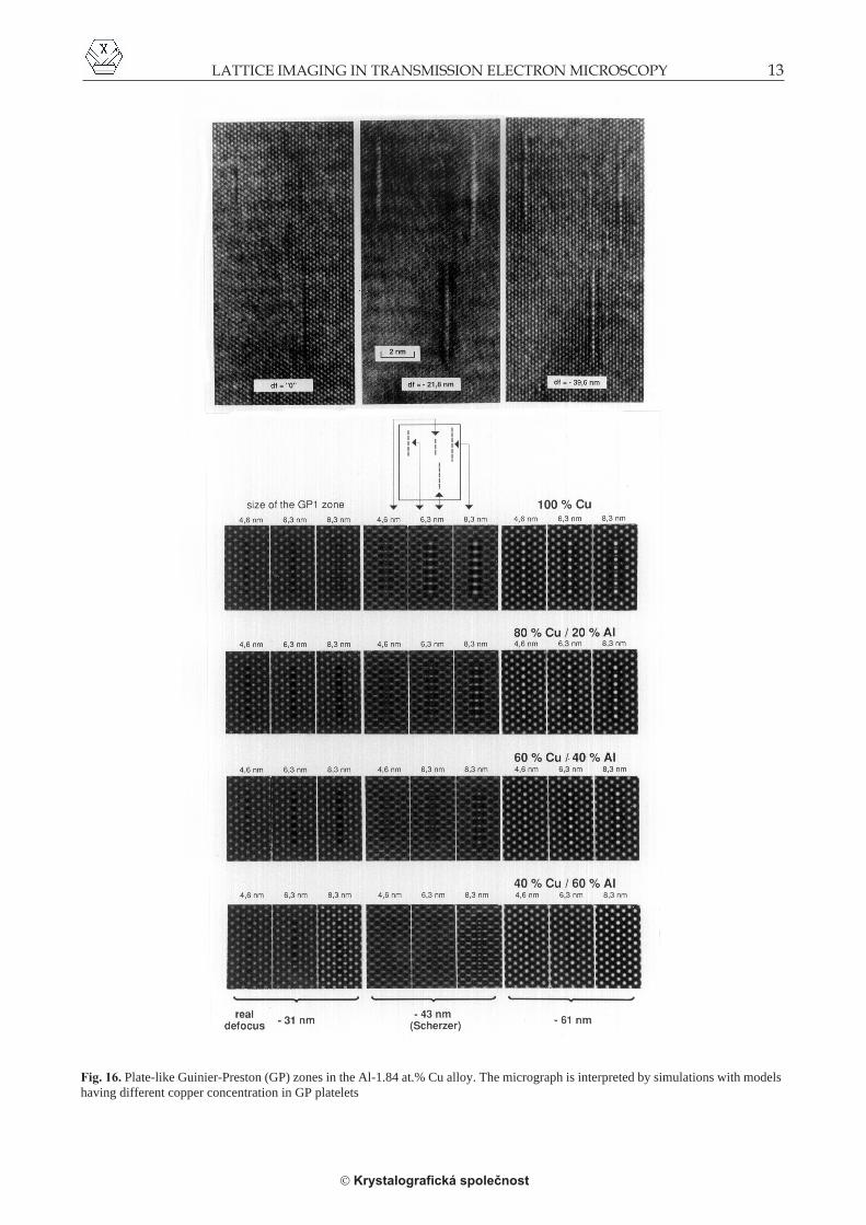
Fig. 13 shows a cross-section of a Si/SiO2 interfaceprepared by a plasma torch. The interface is edge-on, show-ing several ledges and a crystallite formed in the amor-phous SiO2. The Si crystal lattice is imaged in the <110>zone axis, each white dot in the micrograph representingtwo atomic columns (dumbbells) in the diamond structure.In order to separate these columns in the image, a micro-scope with resolution close to 0.1 nm is required.
A next nearest-neighbour antiphase boundary in theordered alloy based on Fe3Al is presented in Fig. 14. Thecrystal defect is edge-on, only Al sublattice of the D03
structure is imaged. The arrows indicate parts of theedge-on imaged defect. The inset in the lower part of themicrograph shows the simulation of the atomic configura-tion of the defect. A defocus-thickness map for this alloy isin Fig. 15. It is clearly seen, that only specific combinationsof crystal thickness and defocus of the objective lens givestructure images. For more details see [21, 22].
� Krystalografická spoleènost
LATTICE IMAGING IN TRANSMISSION ELECTRON MICROSCOPY 11
Fig. 11. Contrast transfer function for a 200 kV and a 400 kV mi-croscope with Cs = 1.2 mm. Positions of hkl planes of aluminiumand silicon are indicated
Fig. 12. Comparison of transfer functions of the same microscopefitted with LaB6 and field emission gun (FEG)
Fig. 13. Crystallite at the interface Si/SiO2 (courtesy M. Froment,Université Pierre et Marie Curie, Paris)
W LaB6 FEG
Temperature [K] 2700 1700 300
Energy spread [eV] 3 1.5 0.3
Size [4m] 50 10 <0.01
Brightness [Am-2srad-1] 109 551010 1013
Current density [Am-2] 55104 106 1010
Table 1. Parameters of electron sources, operating at 100 k
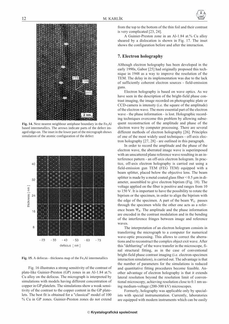
Fig. 16 illustrates a strong sensitivity of the contrast ofplate-like Guinier-Preston (GP) zones in an Al-1.84 at.%Cu alloy on the defocus. The micrograph is interpreted bysimulations with models having different concentration ofcopper in GP platelets. The simulations show a weak sensi-tivity of the contrast to the copper content in the GP plate-lets. The best fit is obtained for a "classical" model of 100% Cu in GP zones. Guinier-Preston zones do not extend
from the top to the bottom of the thin foil and their contrastis very complicated [23, 24].
A Guinier-Preston zone in an Al-1.84 at.% Cu alloysheared by a dislocation is shown in Fig. 17. The insetshows the configuration before and after the interaction.
7. Electron holography
Although electron holography has been developed in theearly 1990s, Gabor [25] had originally proposed this tech-nique in 1948 as a way to improve the resolution of theTEM. The delay in its implementation was due to the lackof sufficiently coherent electron sources - field-emissionguns.
Electron holography is based on wave optics. As wehave seen in the description of the bright-field phase con-trast imaging, the image recorded on photographic plate orCCD-camera is intensity (i.e. the square of the amplitude)of the electron wave. The more essential part of the electronwave - the phase information - is lost. Holographic record-ing techniques overcome this problem by allowing subse-quent reconstruction of the amplitude and phase of theelectron wave by computer processing. There are severaldifferent methods of electron holography [26]. Principlesof one of the most widely used techniques - off-axis elec-tron holography [27, 28] - are outlined in this paragraph.
In order to record the amplitude and the phase of theelectron wave, the aberrated image wave is superimposedwith an unscattered plane reference wave resulting in an in-terference pattern - an off-axis electron hologram. In prac-tice, off-axis electron holography is carried out using afield-emission gun TEM (FEG TEM) equipped with abeam splitter, placed below the objective lens. The beamsplitter is made by a metal coated glass fiber < 0.5 4m in di-ameter, assembled to give electron biprism (Fig. 18). Thevoltage applied on the fiber is positive and ranges from 10to 150 V. It is important to have the possibility to rotate thebiprism or the specimen, in order to align the biprism withthe edge of the specimen. A part of the beam 6G passesthrough the specimen while the other one acts as a refer-ence beam 6R. The amplitude and the phase informationare encoded in the contrast modulation and in the bendingof the interference fringes between image and referencewaves.
The interpretation of an electron hologram consists intransferring the micrograph to a computer for numericalwave-optic processing. This allows to correct the aberra-tions and to reconstruct the complex object exit wave. Afterthis "deblurring" of the wave transfer in the microscope, fi-nal structural fitting, as in the case of conventionalbright-field phase contrast imaging (i.e. electron-specimeninteraction simulation), is carried out. The advantage is thatthe number of parameters for the simulations is reducedand quantitative fitting procedures become feasible. An-other advantage of electron holography is that it extendslateral resolution beyond the resolution limit of conven-tional microscopy, achieving resolution close to 0.1 nm us-ing medium-voltage (200-300 kV) microscopes.
Formerly, holography was applicable only by special-ists with special instrumentation. Currently, laboratoriesare equipped with modern instruments which can be easily
� Krystalografická spoleènost
12 M. KARLÍK
Fig. 15. A defocus - thickness map of the Fe3Al intermetallics
Fig. 14. Next nearest neighbour antiphase boundary in the Fe3Albased intermetallics. The arrows indicate parts of the defect im-aged edge-on. The inset in the lower part of the micrograph showssimulation of the atomic configuration of the defect
� Krystalografická spoleènost
LATTICE IMAGING IN TRANSMISSION ELECTRON MICROSCOPY 13
Fig. 16. Plate-like Guinier-Preston (GP) zones in the Al-1.84 at.% Cu alloy. The micrograph is interpreted by simulations with modelshaving different copper concentration in GP platelets
adapted for off-axis holography. Basic requirements are ahighly-coherent field-emission gun and an electronbiprism.
The range of applications is wide. Off-axis electron ho-lography is used for the analysis of structures with atomicresolution. However there are more applications with
lower resolution, such as measurements of doping profilesin pn-junctions, imaging of electric and magnetic fieldswith lateral resolution of a few nanometers, doping analy-sis in interfaces etc. [29].
8. Z-contrast imaging
Allowing incoherent imaging, the Z-contrast techniquerepresents a new approach to atomic resolution electronmicroscopy. It provides directly interpretable images -maps of scattering power of the specimen [30]. This tech-nique is most easily implemented in a (dedicated) scanningtransmission electron microscope (STEM) [4]. Many con-ventional TEMs are also equipped with scanning facilitiesand electron detectors and they can be used also in a scan-ning transmission mode [31]. The STEM image is obtainedby scanning an electron probe of atomic dimensions acrossthe specimen and collecting electrons by a post-specimendetector (Fig. 19). Scan coils raster the probe across thespecimen and their current is used to raster simultaneouslythe beam of a cathode ray tube (CRT). The signal propor-tional to intensity of electrons scattered and detected by anelectron detector is then displayed on CRT, each pixel onthe CRT showing intensity of a part of the image. The per-sistence of the screen phosphor fluorescence, or frame-store electronics allow the operator to see the whole image.Digital image acquisition is a natural consequence of thismode of operation.
Magnification of the image is given by the ratio of theCRT viewing area dimensions and dimensions of thescanned area. If the scanned area on the specimen is 1 4m 5
� Krystalografická spoleènost
14 M. KARLÍK
Fig. 18. Principle of off-axis electron holography
Fig. 17. A Guinier-Preston zone sheared by a dislocation
Fig. 19. Principle of a scanning-transmission electron microscope(STEM)
1 4m and the resulting image is displayed on a CRT withthe area of 10 cm 5 10 cm, the magnification is 100 000 5.Resolution of the technique is determined by the size of thefocused electron probe.
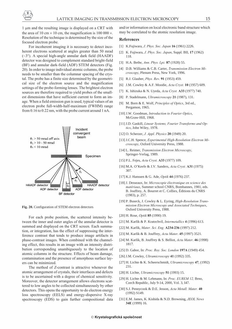
For incoherent imaging it is necessary to detect inco-herent electrons scattered at angles greater than 50 mrad(~3°). A special high-angle annular dark field (HAADF)detector was designed to complement standard bright-field(BF) and annular dark-field (ADF) STEM detectors (Fig.20). In order to image individual atomic columns, the probeneeds to be smaller than the columnar spacing of the crys-tal. The probe has a finite size determined by the geometri-cal size of the electron source and the magnificationsettings of the probe-forming lenses. The brightest electronsources are therefore required to yield probes of the small-est dimensions that have sufficient current to form an im-age. When a field emission gun is used, typical values of anelectron probe full-width-half-maximum (FWHM) rangefrom 0.16 to 0.22 nm, with the probe current around 1 nA.
For each probe position, the scattered intensity be-tween the inner and outer angles of the annular detector issummed and displayed on the CRT screen. Each summa-tion, or integration, has the effect of suppressing the inter-ference contrast that tends to produce image artifacts inphase-contrast images. When combined with the channel-ing effect, this results in an image with an intensity distri-bution corresponding unambiguously to the location ofatomic columns in the structure. Effects of beam damage,contamination and the presence of amorphous surface lay-ers can be minimized.
The method of Z-contrast is attractive whenever theatomic arrangement of crystals, their interfaces and defectsis to be ascertained with a degree of chemical sensitivity.Moreover, the detector arrangement allows electrons scat-tered to low angles to be collected simultaneously by otherdetectors. This opens the opportunity to do electron energyloss spectroscopy (EELS) and energy-dispersive X-rayspectroscopy (EDS) to gain further compositional data
and/or information on local electronic band structure whichmay be correlated to the atomic resolution image.
References
[1] K.Fujiwara, J. Phys. Soc. Japan 16 (1961) 2226.
[2] K. Fujiwara, J. Phys. Soc. Japan, Suppl. BII, 17 (1962)118.
[3] H.A. Bethe, Ann. Phys. Lpz. 87 (1928) 55.
[4] D.B. Williams & C.B. Carter, Transmission Electron Mi-
croscopy, Plenum Press, New York, 1996.
[5] R.J. Glauber, Phys. Rev. 91 (1953) 459.
[6] J.M. Cowley & A.F. Moodie, Acta Cryst. 10 (1957) 609.
[7] K. Ishizuka & N. Uyeda, Acta Cryst. A33 (1977) 740.
[8] P. Stadelmann, Ultramicroscopy 21 (1987), 131.
[9] M. Born & E. Wolf, Principles of Optics, 3rd ed.,Pergamon, 1965.
[10] J.W. Goodman, Introduction to Fourier Optics,McGraw-Hill, 1968.
[11] J.D. Gaskill, Linear Systems, Fourier Transforms and Op-
tics, John Wiley, 1978.
[12] O. Scherzer, J. Appl. Physics 20 (1949) 20.
[13] J.C.H. Spence, Experimental High-Resolution Electron Mi-
croscopy, Oxford University Press, 1988.
[14] L. Reimer, Transmission Electron Microscopy,Springer-Verlag, 1989.
[15] P.L. Fejes, Acta Cryst. A33 (1977) 109.
[16] M.A. O’Keefe & J.V. Sanders, Acta Cryst. A31 (1975)307.
[17] K.J. Hanssen & G. Ade, Optik 44 (1976) 237.
[18] J. Desseaux, In: Microscopie électronique en science des
matériaux, Summer school CNRS, Bombannes, 1981, eds.B. Jouffrey, A. Bourret et C. Colliex, Éditions du CNRS(1983), p. 257.
[19] P. Buseck, J. Cowley & L. Eyring, High-Resolution Trans-
mission Electron Microscopy and Associated Techniques,Oxford University Press, 1988.
[20] H. Rose, Optik 85 (1990) 19.
[21] M. Karlík & P. Kratochvíl, Intermetallics 4 (1996) 613.
[22] M. Karlík, Mater. Sci. Eng. A234-236 (1997) 212.
[23] M. Karlík & B. Jouffrey, Acta Mater. 45 (1997) 3521.
[24] M. Karlík, B. Jouffrey & S. Belliot, Acta Mater. 46 (1998)1817.
[25] D. Gabor, In: Proc. Roy. Soc. London 197A (1949) 454.
[26] J.M. Cowley, Ultramicroscopy 41 (1992) 335.
[27] H. Lichte & K. Scheerschmidt, Ultramicroscopy 47, (1992)231.
[28] H. Lichte, Ultramicroscopy 51 (1993) 15.
[29] H. Lichte & M. Lehmann, In: Proc. EUREM 12, Brno,Czech Republic, July 9-14, 2000, Vol. 3, I47.
[30] S.J. Pennycook & D.E. Jesson, Acta Metall. Mater. 40
(1992) S149.
[31] E.M. James, K. Kishida & N.D. Browning, JEOL News
34E (1999) 16.
� Krystalografická spoleènost
LATTICE IMAGING IN TRANSMISSION ELECTRON MICROSCOPY 15
Fig. 20. Configuration of STEM electron detectors

� Krystalografická spoleènost
16 M. KARLÍK