Latest Developments in X-ray Photoelectron Spectroscopy ... · (Auger electron spectroscopy,...
48
A Shimadzu Group Company A Shimadzu Group Company www.kratos.com D. Surman Ph.D., Kratos Analytical Inc., Chestnut Ridge, NY 10977 Latest Developments in X-ray Photoelectron Spectroscopy and their Application to Nanosurfaces
Transcript of Latest Developments in X-ray Photoelectron Spectroscopy ... · (Auger electron spectroscopy,...

A Shimadzu Group CompanyA Shimadzu Group Company
www.kratos.com
D. Surman Ph.D., Kratos Analytical Inc., Chestnut Ridge, NY 10977
Latest Developments in X-ray Photoelectron Spectroscopy and their Application to Nanosurfaces
A Shimadzu Group CompanyA Shimadzu Group Company
Outline of Presentation
• Brief discussion of the technique– Relationship of the technique with other analytical methods– Relevance of the technique to nano-applications– Fundamentals of the technique
• What types of information does the technique provide
– Developments and Applications of the technique• General information
• Nano-scale information– Application of Angle Resolved XPS to provide nano-scale depth
information
– Extension to macro-scale depth information
• Lateral information– 2D imaging
• 3D information– Sputter depth profiling
A Shimadzu Group CompanyA Shimadzu Group Company
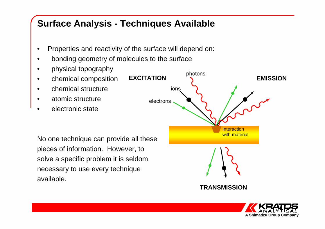
• Properties and reactivity of the surface will depend on:
• bonding geometry of molecules to the surface
• physical topography• chemical composition
• chemical structure
• atomic structure• electronic state
No one technique can provide all these
pieces of information. However, to
solve a specific problem it is seldom necessary to use every technique
available.
photons
ions
electrons
EMISSION
TRANSMISSION
Interaction with material
EXCITATION
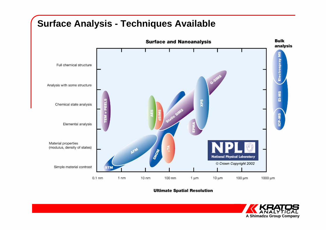
Surface Analysis - Techniques Available
A Shimadzu Group CompanyA Shimadzu Group Company
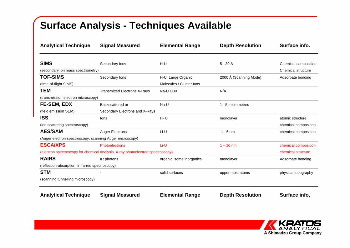
Analytical Technique Signal Measured Elemental Rang e Depth Resolution Surface info.
SIMS Secondary Ions H-U 5 - 30 Å Chemical composition
(secondary ion mass spectrometry) Chemical structure
TOF-SIMS Secondary Ions H-U, Large Organic 2000 Å (Scanning Mode) Adsorbate bonding
(time-of-flight SIMS) Molecules / Cluster Ions
TEM Transmitted Electrons X-Rays Na-U EDX N/A
(transmission electron microscopy)
FE-SEM, EDX Backscattered or Na-U 1 - 5 micrometres
(field emission SEM) Secondary Electrons and X-Rays
ISS Ions H- U monolayer atomic structure
(ion scattering spectroscopy) chemical composition
AES/SAM Auger Electrons Li-U 1 - 5 nm chemical composition
(Auger electron spectroscopy, scanning Auger microscopy)
ESCA/XPS Photoelectrons Li-U 1 – 10 nm chemical composition
(electron spectroscopy for chemical analysis, X-ray photoelectron spectroscopy) chemical structure
RAIRS IR photons organic, some inorganics monolayer Adsorbate bonding
(reflection-absorption infra-red spectroscopy)
STM - solid surfaces upper most atoms physical topography
(scanning tunnelling microscopy)
Analytical Technique Signal Measured Elemental Range Depth Resolution Surface info,
Surface Analysis - Techniques Available
A Shimadzu Group CompanyA Shimadzu Group Company
Surface Analysis - Techniques Available
A Shimadzu Group CompanyA Shimadzu Group Company
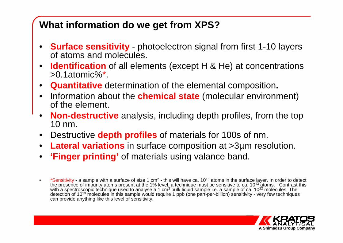
What information do we get from XPS?
• Surface sensitivity - photoelectron signal from first 1-10 layers of atoms and molecules.
• Identification of all elements (except H & He) at concentrations >0.1atomic%*.
• Quantitative determination of the elemental composition.• Information about the chemical state (molecular environment)
of the element.• Non-destructive analysis, including depth profiles, from the top
10 nm.• Destructive depth profiles of materials for 100s of nm.• Lateral variations in surface composition at >3µm resolution.• ‘Finger printing’ of materials using valance band.
• *Sensitivity - a sample with a surface of size 1 cm2 - this will have ca. 1015 atoms in the surface layer. In order to detect the presence of impurity atoms present at the 1% level, a technique must be sensitive to ca. 1013 atoms. Contrast this with a spectroscopic technique used to analyse a 1 cm3 bulk liquid sample i.e. a sample of ca. 1022 molecules. The detection of 1013 molecules in this sample would require 1 ppb (one part-per-billion) sensitivity - very few techniques can provide anything like this level of sensitivity.
A Shimadzu Group CompanyA Shimadzu Group Company
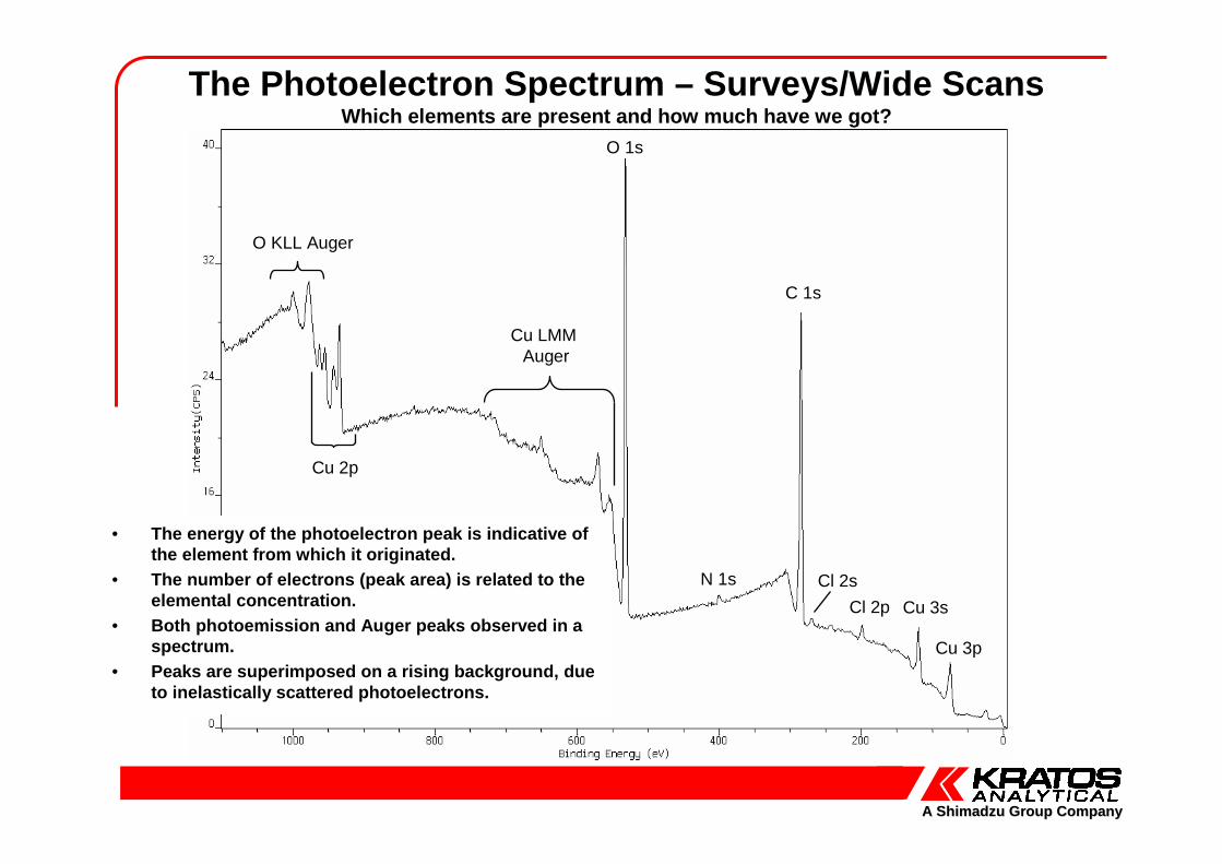
The Photoelectron Spectrum – Surveys/Wide ScansWhich elements are present and how much have we got ?
Cu 2p
O KLL Auger
O 1s
N 1s
C 1s
Cu LMM Auger
Cu 3p
Cu 3sCl 2p
Cl 2s
• The energy of the photoelectron peak is indicative of the element from which it originated.
• The number of electrons (peak area) is related to t he elemental concentration.
• Both photoemission and Auger peaks observed in a spectrum.
• Peaks are superimposed on a rising background, due to inelastically scattered photoelectrons.
A Shimadzu Group CompanyA Shimadzu Group Company
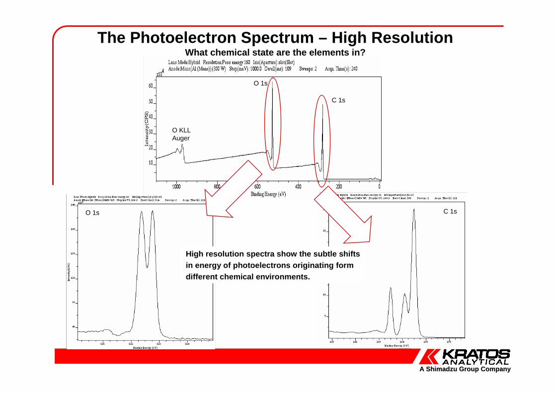
O 1s
C 1s
O KLLAuger
O 1s C 1s
The Photoelectron Spectrum – High ResolutionWhat chemical state are the elements in?
High resolution spectra show the subtle shiftsin energy of photoelectrons originating formdifferent chemical environments.
A Shimadzu Group CompanyA Shimadzu Group Company
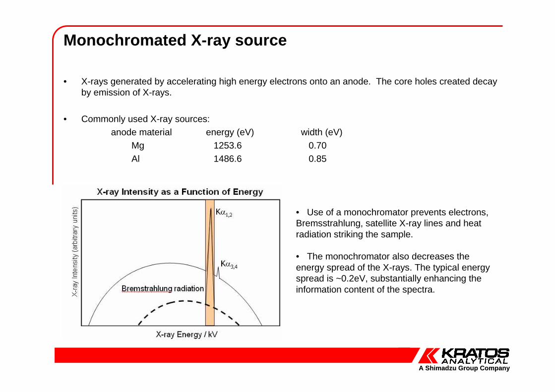
• X-rays generated by accelerating high energy electrons onto an anode. The core holes created decay by emission of X-rays.
• Commonly used X-ray sources:anode material energy (eV) width (eV)
Mg 1253.6 0.70Al 1486.6 0.85
• Use of a monochromator prevents electrons, Bremsstrahlung, satellite X-ray lines and heat radiation striking the sample.
• The monochromator also decreases the energy spread of the X-rays. The typical energy spread is ~0.2eV, substantially enhancing the information content of the spectra.
Monochromated X-ray source

A Shimadzu Group CompanyA Shimadzu Group Company
Developments in Monochromator technology
Toroidal quartz backplane
Electron gun & x-ray anode
Rowland circle diameter
Enhancements to the source design to improve small area intensity include filament design and power dissipation technology.These increase flux and therefore sensitivity (detection levels)
Modifications to the crystal geometry improve focusing of the optics for smaller irradiated areas. This increased x-ray flux density at the sample enhances sensitivity.
Changes to the Rowland circle modifies the performance of the monochromator to match energy resolution or spatial resolution requirements
A Shimadzu Group CompanyA Shimadzu Group Company
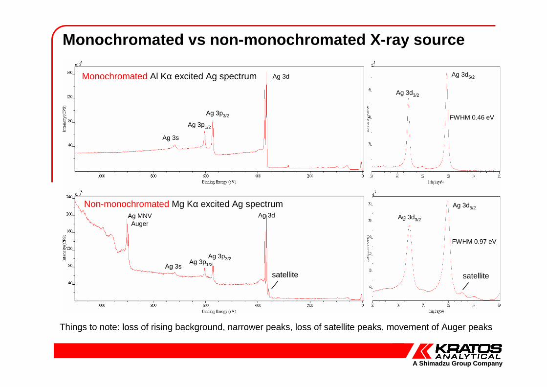
Monochromated vs non-monochromated X-ray source
Monochromated Al Kα excited Ag spectrum
Non-monochromated Mg Kα excited Ag spectrum
FWHM 0.97 eV
FWHM 0.46 eV
satellite
Things to note: loss of rising background, narrower peaks, loss of satellite peaks, movement of Auger peaks
Ag 3d
Ag 3p3/2
Ag 3p1/2
Ag 3p3/2Ag 3p1/2
Ag 3d5/2
Ag 3d3/2
Ag 3d5/2
Ag 3d3/2Ag 3d
Ag 3s
Ag 3s
Ag MNV Auger
satellite
A Shimadzu Group CompanyA Shimadzu Group Company
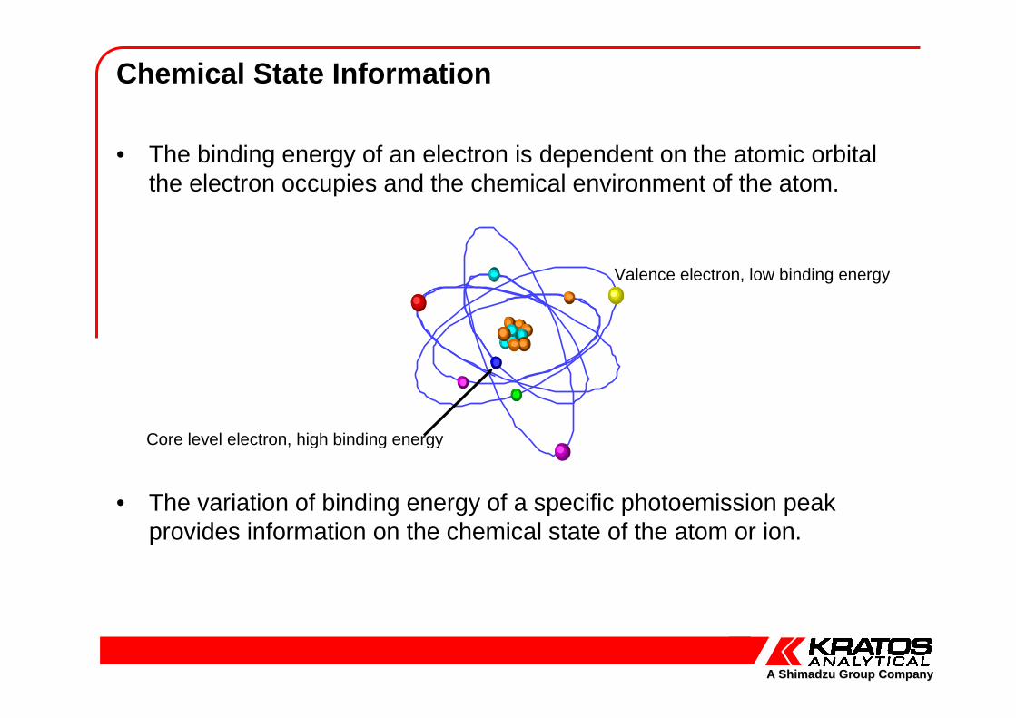
Chemical State Information
• The binding energy of an electron is dependent on the atomic orbital the electron occupies and the chemical environment of the atom.
• The variation of binding energy of a specific photoemission peakprovides information on the chemical state of the atom or ion.
Core level electron, high binding energy
Valence electron, low binding energy
A Shimadzu Group CompanyA Shimadzu Group Company
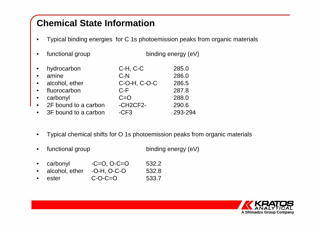
Chemical State Information
• Typical binding energies for C 1s photoemission peaks from organic materials
• functional group binding energy (eV)
• hydrocarbon C-H, C-C 285.0• amine C-N 286.0• alcohol, ether C-O-H, C-O-C 286.5• fluorocarbon C-F 287.8• carbonyl C=O 288.0• 2F bound to a carbon -CH2CF2- 290.6• 3F bound to a carbon -CF3 293-294
• Typical chemical shifts for O 1s photoemission peaks from organic materials
• functional group binding energy (eV)
• carbonyl -C=O, O-C=O 532.2• alcohol, ether -O-H, O-C-O 532.8• ester C-O-C=O 533.7
A Shimadzu Group CompanyA Shimadzu Group Company
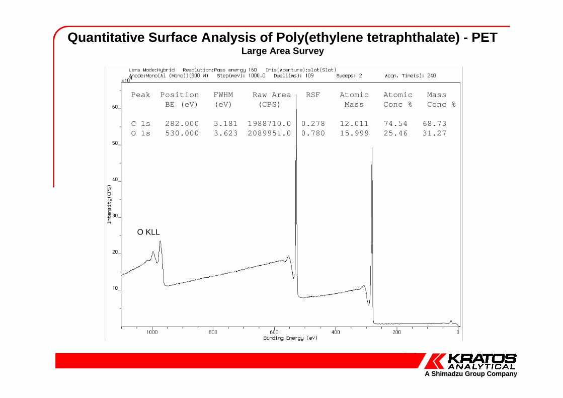
Quantitative Surface Analysis of Poly(ethylene tetraph thalate) - PET Large Area Survey
O KLL
Peak Position FWHM Raw Area RSF Atomic Atomic Mass BE (eV) (eV) (CPS) Mass Conc % Conc %
C 1s 282.000 3.181 1988710.0 0.278 12.011 74.54 68.73 O 1s 530.000 3.623 2089951.0 0.780 15.999 25.46 31.27
A Shimadzu Group CompanyA Shimadzu Group Company
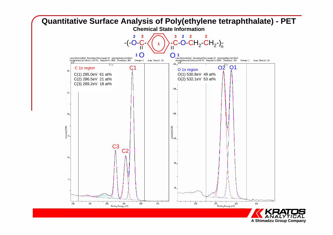
Quantitative Surface Analysis of Poly(ethylene tetraph thalate) - PETChemical State Information
C 1s region O 1s regionO(1) 530.8eV 49 at% O(2) 532.1eV 53 at%
C(1) 285.0eV 61 at%C(2) 286.5eV 21 at%C(3) 289.2eV 18 at%
C3C2
C1 O1O2
-(-O-C- -C-O-CH2-CH2-)-= =
O On
2223
1
32
1
1
A Shimadzu Group CompanyA Shimadzu Group Company
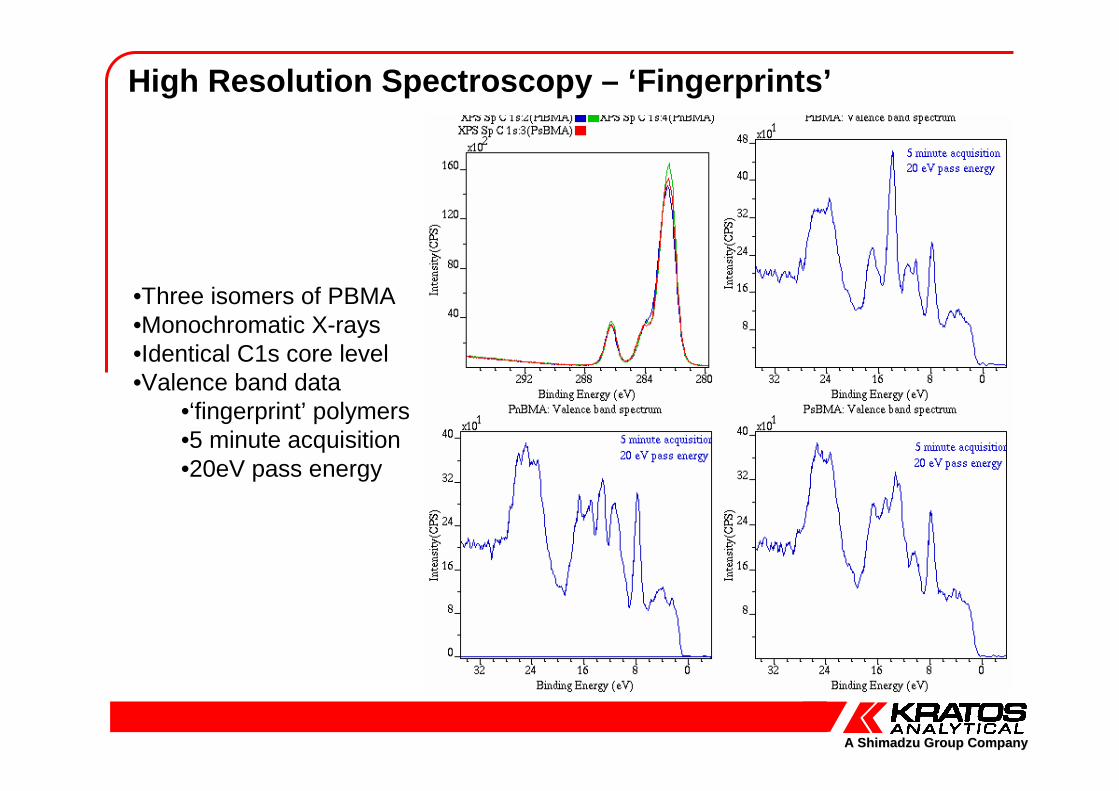
High Resolution Spectroscopy – ‘Fingerprints’
•Three isomers of PBMA•Monochromatic X-rays•Identical C1s core level•Valence band data
•‘fingerprint’ polymers•5 minute acquisition•20eV pass energy
A Shimadzu Group CompanyA Shimadzu Group Company
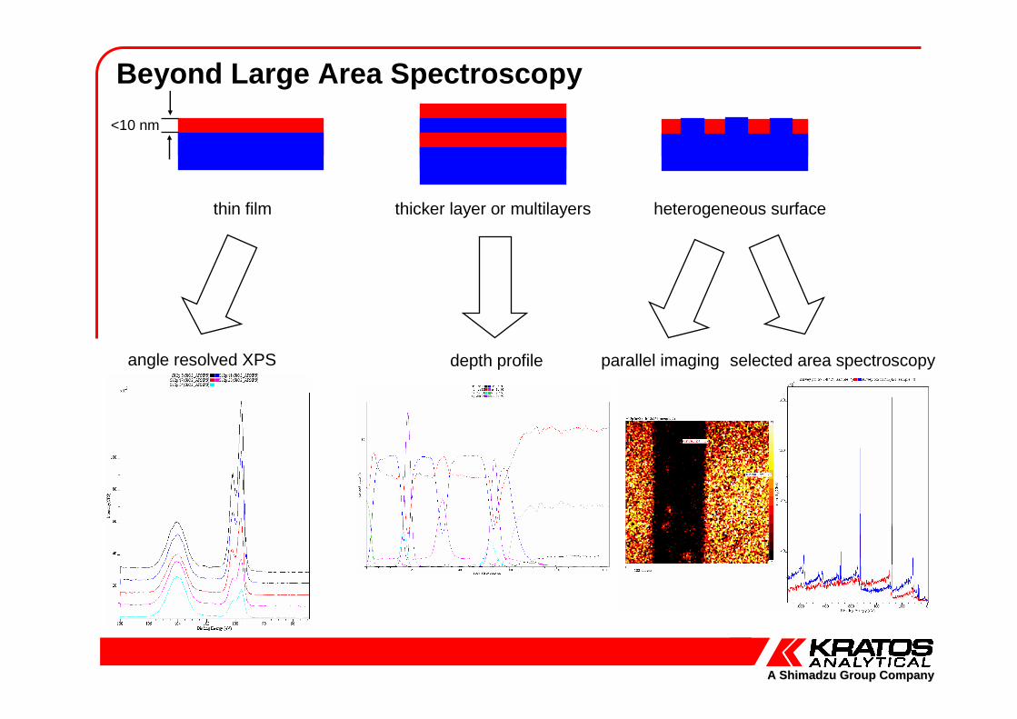
Beyond Large Area Spectroscopy
thin film
<10 nm
thicker layer or multilayers heterogeneous surface
angle resolved XPS depth profile parallel imaging selected area spectroscopy
A Shimadzu Group CompanyA Shimadzu Group Company
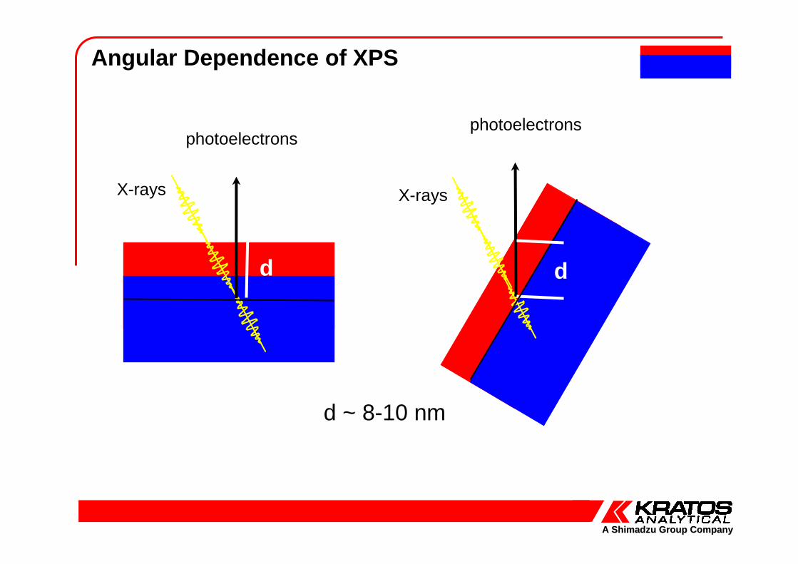
Angular Dependence of XPS
d
d ~ 8-10 nm
d
photoelectrons
X-rays
photoelectrons
X-rays

A Shimadzu Group CompanyA Shimadzu Group Company
Angular Dependence of XPS - SiO 2 on Si wafer
0 deg (bulk sensitive)
60 degrees
45 degrees
75 degrees(surface sensitive)
Si elemental
Si oxide
A Shimadzu Group CompanyA Shimadzu Group Company
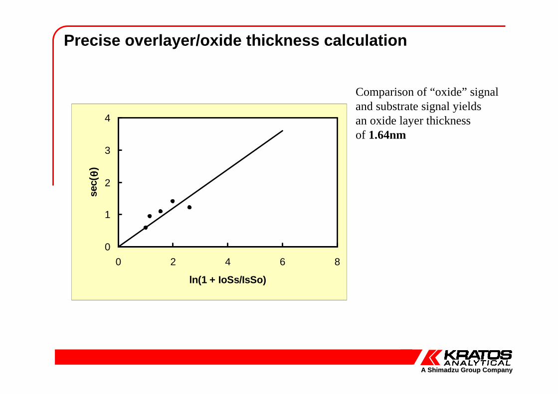
Precise overlayer/oxide thickness calculation
0
1
2
3
4
0 2 4 6 8
ln(1 + IoSs/IsSo)
sec(
θθ θθ)Comparison of “oxide” signal and substrate signal yields an oxide layer thickness of 1.64nm
A Shimadzu Group CompanyA Shimadzu Group Company
Development of ARXPS for nano-scale information
• Application of MEM’s methodology to ARXPS results– assumptions postulated by the model used in MEM calculations :
• the electron transport in the sample must be determined by the inelastic scattering with the constant mean free path throughout the sample and the material density must be constant throughout the sample.
• The necessary condition for the consistency of experimentally measured data with the MEM model (successful fit) is that the Laplace transform of the compositional depth profile (LTCDP) calculated from the experimentally measured normalized intensity is a monotonically decreasing function for all measured elements.
– Enhancements to the MEM’s methodology
• Development of an efficient algorithm which can estimate the LTCDP for elements with different inelastic mean free paths and thus provide an independent estimate of the noise scaling calculated by the MEMSYS algorithm and verify whether the MEM model is appropriate for the measured data.
A Shimadzu Group CompanyA Shimadzu Group Company
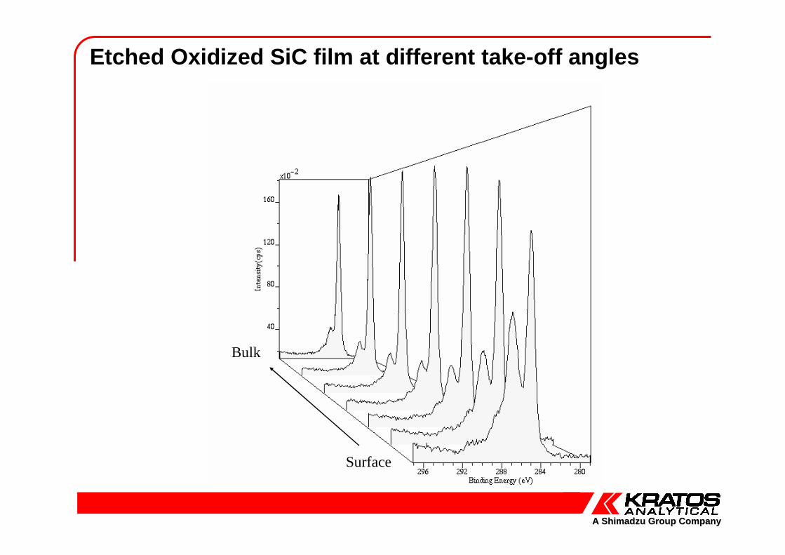
Etched Oxidized SiC film at different take-off angle s
Surface
Bulk
A Shimadzu Group CompanyA Shimadzu Group Company
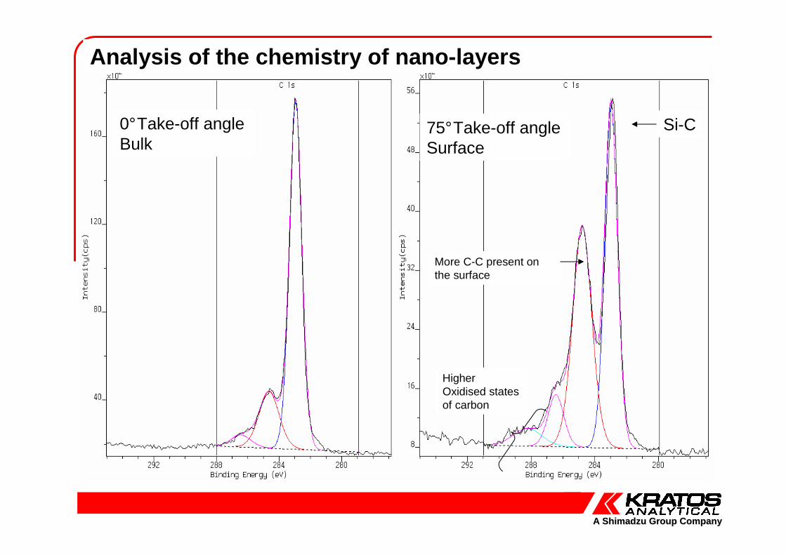
0°Take-off angleBulk
75°Take-off angleSurface
More C-C present on the surface
Higher Oxidised states of carbon
Si-C
Analysis of the chemistry of nano-layers
A Shimadzu Group CompanyA Shimadzu Group Company
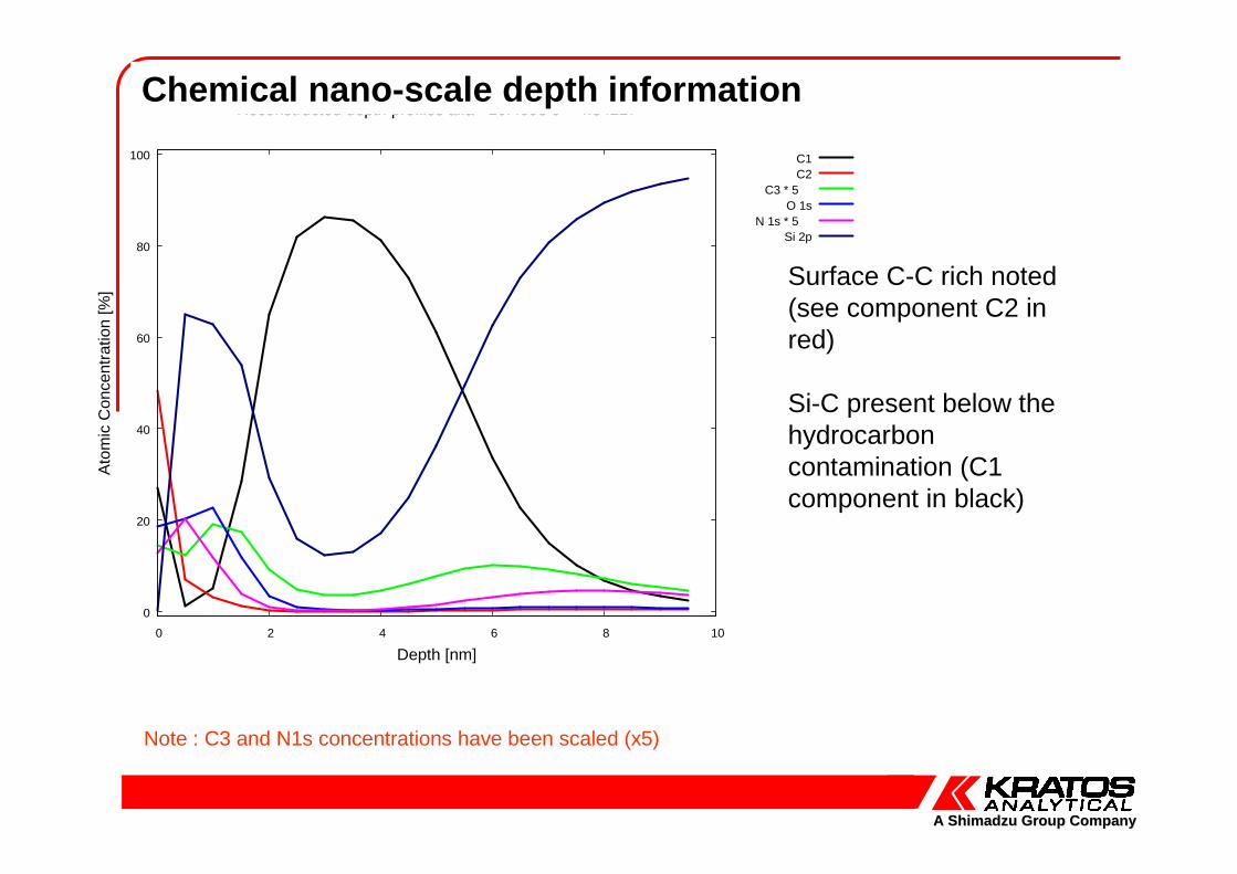
Surface C-C rich noted (see component C2 in red)
Si-C present below the hydrocarbon contamination (C1 component in black)
Note : C3 and N1s concentrations have been scaled (x5)
0
20
40
60
80
100
0 2 4 6 8 10
Ato
mic
Con
cent
ratio
n [%
]
Depth [nm]
Reconstructed depth profiles alfa =10.4093 c = 4.34217
C1C2
C3 * 5 O 1s
N 1s * 5 Si 2p
Chemical nano-scale depth information
A Shimadzu Group CompanyA Shimadzu Group Company
Development of lateral information
• Implementation of spherical mirror analyzer opened up new avenues for the detection of laterally resolved information– Spherical mirror provides a real-time energy resolved image of the
distribution of photoelectrons from the surface.• Initial detection systems provided only a qualitative distribution
• Development and implementation of the Delay Line Detector enabled directly quantifiable images to be obtained
• Development and implementation of mathematical models have enhanced the information content of the images to provide quantitative information from single pixels.
A Shimadzu Group CompanyA Shimadzu Group Company
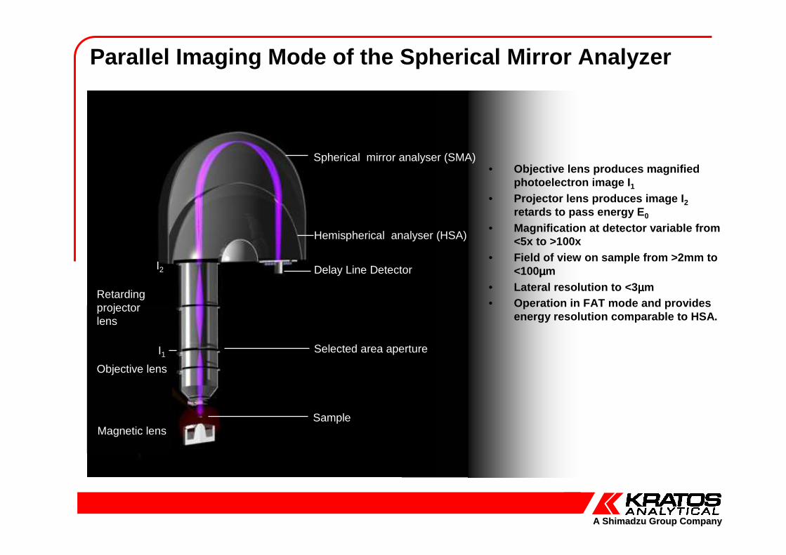
Parallel Imaging Mode of the Spherical Mirror Analy zer
Outer hemisphere of HSA
Charge neutraliser
Spherical mirror analyser (SMA)
Hemispherical analyser (HSA)
Magnetic lensSample
Selected area aperture
Objective lens
Delay Line Detector
Retarding projectorlens
• Objective lens produces magnified photoelectron image I 1
• Projector lens produces image I 2retards to pass energy E 0
• Magnification at detector variable from <5x to >100x
• Field of view on sample from >2mm to <100µµµµm
• Lateral resolution to <3 µµµµm• Operation in FAT mode and provides
energy resolution comparable to HSA.
I1
I2
A Shimadzu Group CompanyA Shimadzu Group Company
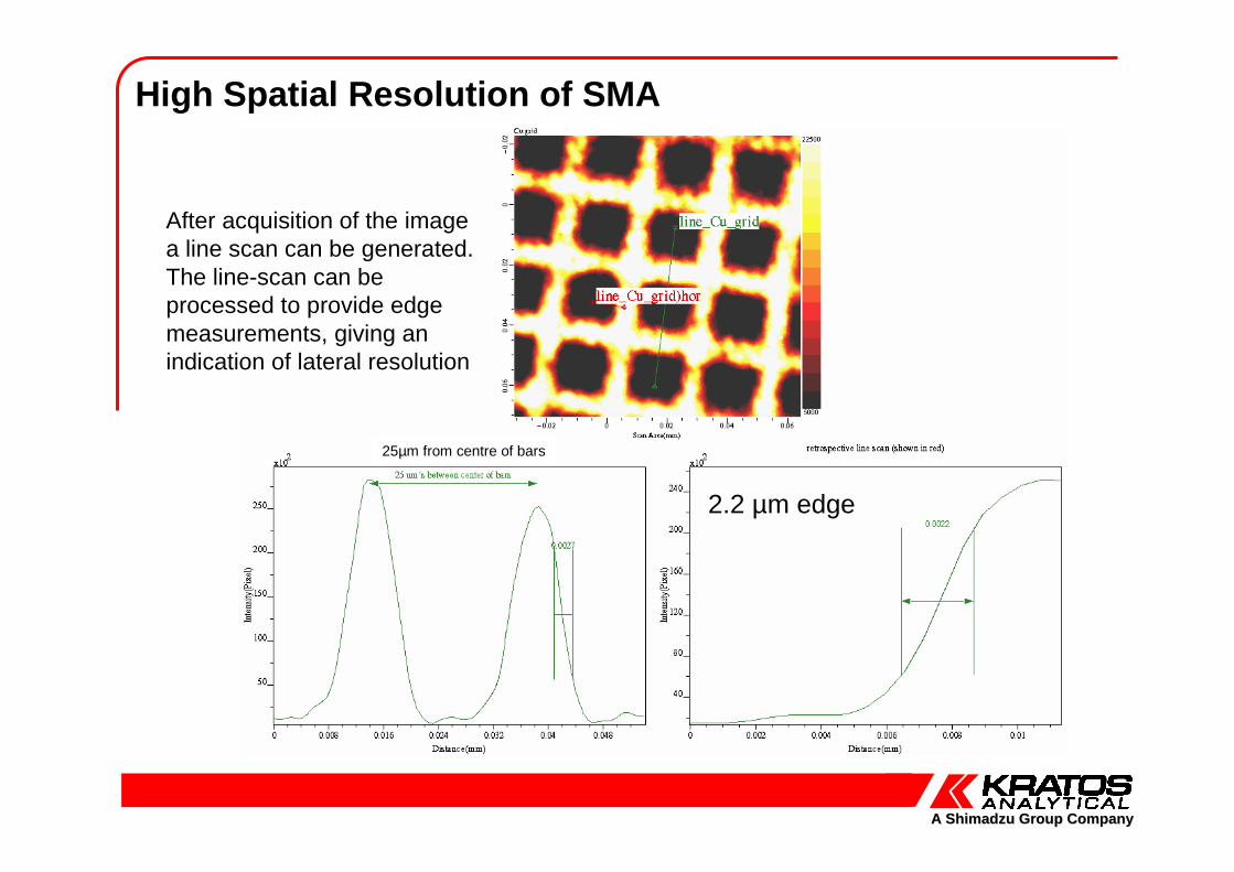
High Spatial Resolution of SMA
2.2 µm edge
25µm from centre of bars
After acquisition of the image a line scan can be generated. The line-scan can be processed to provide edge measurements, giving an indication of lateral resolution
A Shimadzu Group CompanyA Shimadzu Group Company
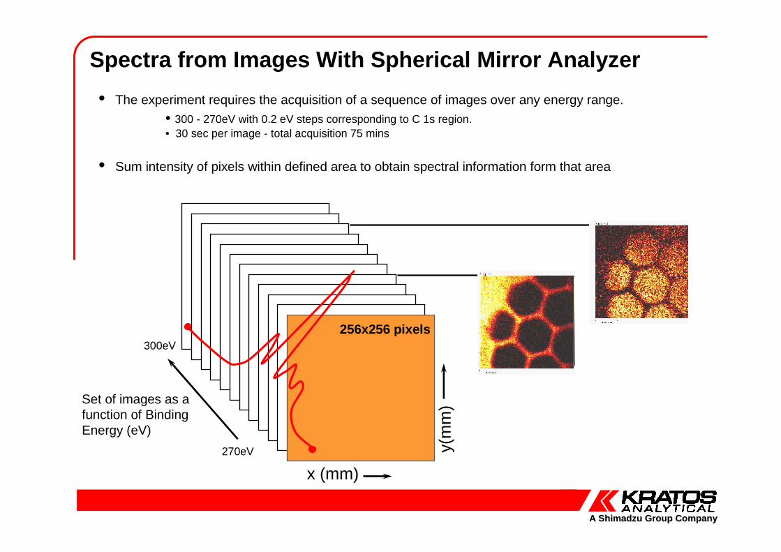
Set of images as a function of Binding Energy (eV)
x (mm)
y(m
m)
256x256 pixels
270eV
300eV
Spectra from Images With Spherical Mirror Analyzer
• The experiment requires the acquisition of a sequence of images over any energy range.• 300 - 270eV with 0.2 eV steps corresponding to C 1s region.• 30 sec per image - total acquisition 75 mins
• Sum intensity of pixels within defined area to obtain spectral information form that area
A Shimadzu Group CompanyA Shimadzu Group Company
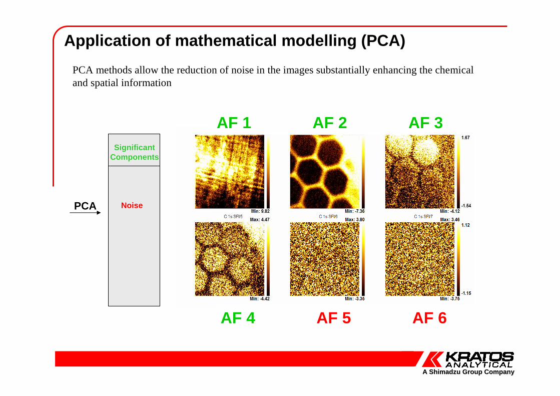
Application of mathematical modelling (PCA)
SignificantComponents
Noise
AF 1 AF 2 AF 3
AF 4 AF 5 AF 6
PCA
PCA methods allow the reduction of noise in the images substantially enhancing the chemical and spatial information
A Shimadzu Group CompanyA Shimadzu Group Company
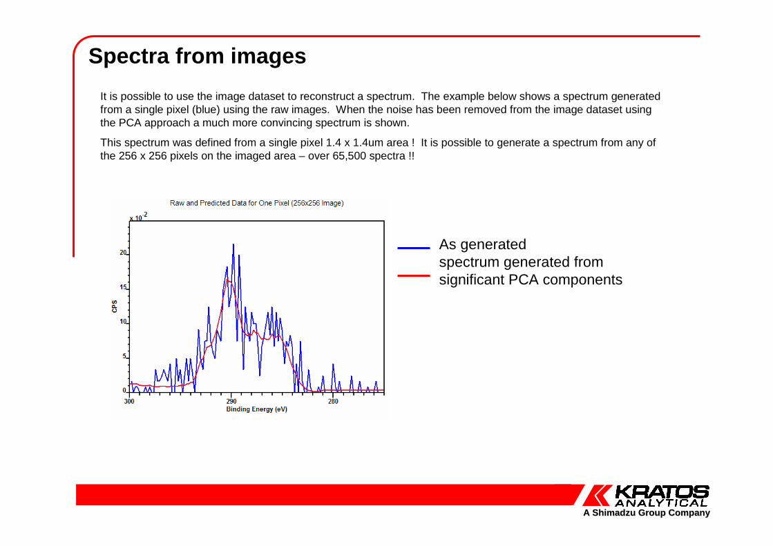
Spectra from images
As generatedspectrum generated from significant PCA components
It is possible to use the image dataset to reconstruct a spectrum. The example below shows a spectrum generated from a single pixel (blue) using the raw images. When the noise has been removed from the image dataset using the PCA approach a much more convincing spectrum is shown.
This spectrum was defined from a single pixel 1.4 x 1.4um area ! It is possible to generate a spectrum from any of the 256 x 256 pixels on the imaged area – over 65,500 spectra !!
A Shimadzu Group CompanyA Shimadzu Group Company
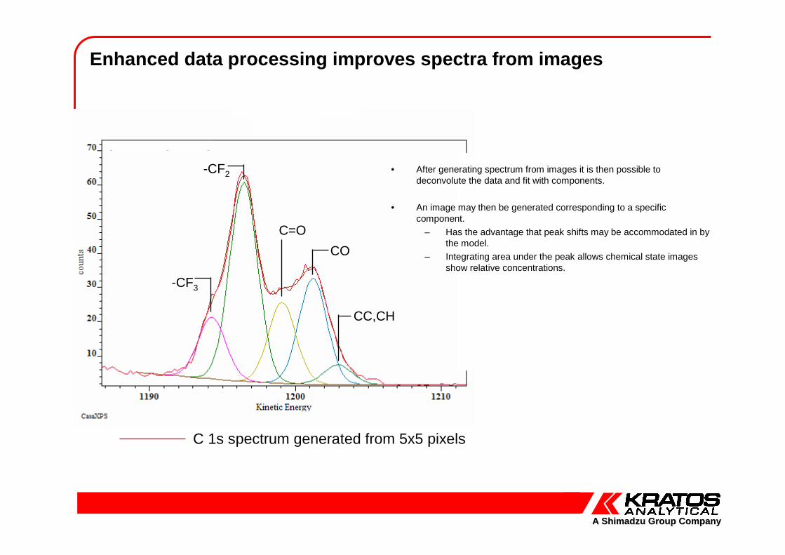
C 1s spectrum generated from 5x5 pixels
CC,CH
CO
C=O
-CF2
-CF3
Enhanced data processing improves spectra from images
• After generating spectrum from images it is then possible to deconvolute the data and fit with components.
• An image may then be generated corresponding to a specific component.
– Has the advantage that peak shifts may be accommodated in by the model.
– Integrating area under the peak allows chemical state images show relative concentrations.
A Shimadzu Group CompanyA Shimadzu Group Company
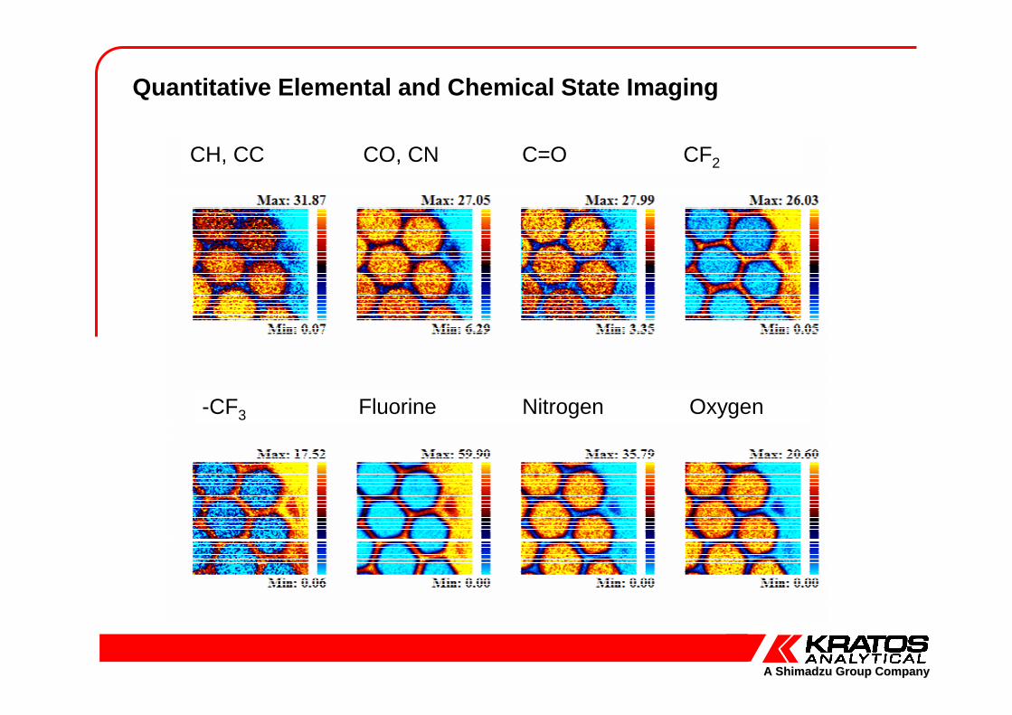
Quantitative Elemental and Chemical State Imaging
CH, CC CO, CN C=O CF2
-CF3 Fluorine Nitrogen Oxygen
A Shimadzu Group CompanyA Shimadzu Group Company
Advantages of imaging for biologically active surfa ces
• Surface and bulk compositions not always the same– Micro-contact angle measurements produce different results from
that predicted by bulk composition– Surface properties are critical in determining bonding of proteins
etc.– Imaging XPS can detect and indicate subtle changes in the surface
composition which lead to changes in the material’s ability to separate different proteins
A Shimadzu Group CompanyA Shimadzu Group Company
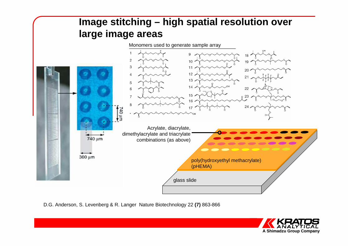
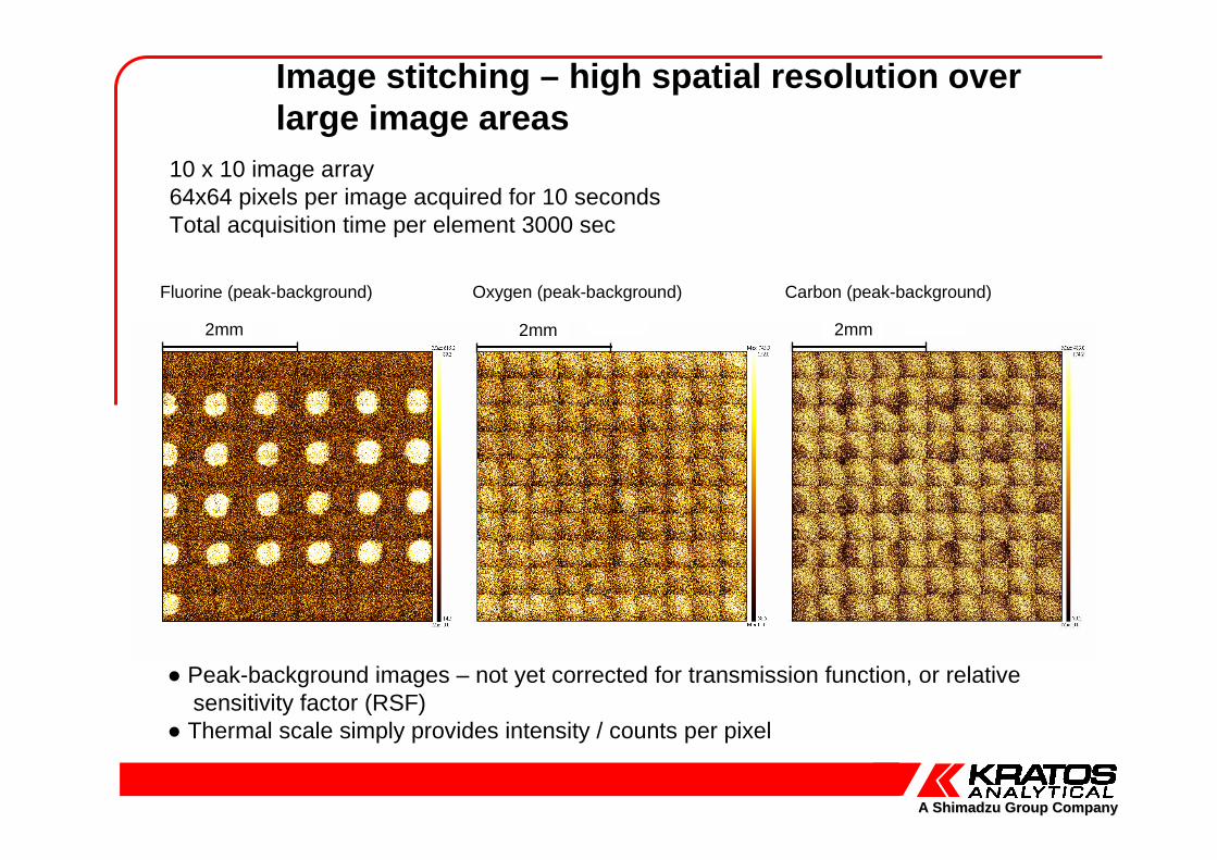
Image stitching – high spatial resolution over large image areas
glass slide
poly(hydroxyethyl methacrylate)(pHEMA)
Acrylate, diacrylate, dimethylacrylate and triacrylate
combinations (as above)
D.G. Anderson, S. Levenberg & R. Langer Nature Biotechnology 22 (7) 863-866
Monomers used to generate sample array
A Shimadzu Group CompanyA Shimadzu Group Company
2mm 2mm 2mm
Fluorine (peak-background) Oxygen (peak-background) Carbon (peak-background)
Image stitching – high spatial resolution over large image areas
● Peak-background images – not yet corrected for transmission function, or relativesensitivity factor (RSF)
● Thermal scale simply provides intensity / counts per pixel
10 x 10 image array 64x64 pixels per image acquired for 10 secondsTotal acquisition time per element 3000 sec
A Shimadzu Group CompanyA Shimadzu Group Company
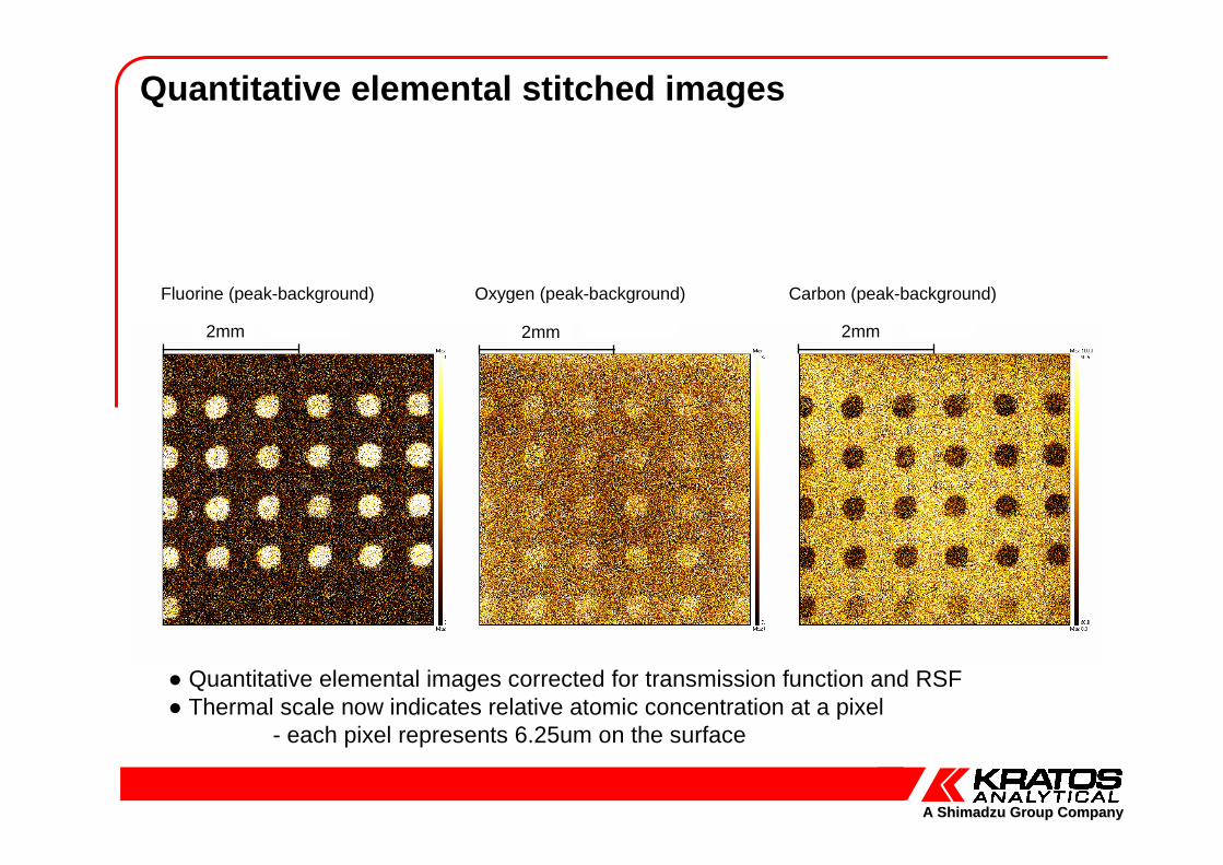
Quantitative elemental stitched images
2mm 2mm 2mm
Fluorine (peak-background) Oxygen (peak-background) Carbon (peak-background)
● Quantitative elemental images corrected for transmission function and RSF● Thermal scale now indicates relative atomic concentration at a pixel
- each pixel represents 6.25um on the surface
A Shimadzu Group CompanyA Shimadzu Group Company
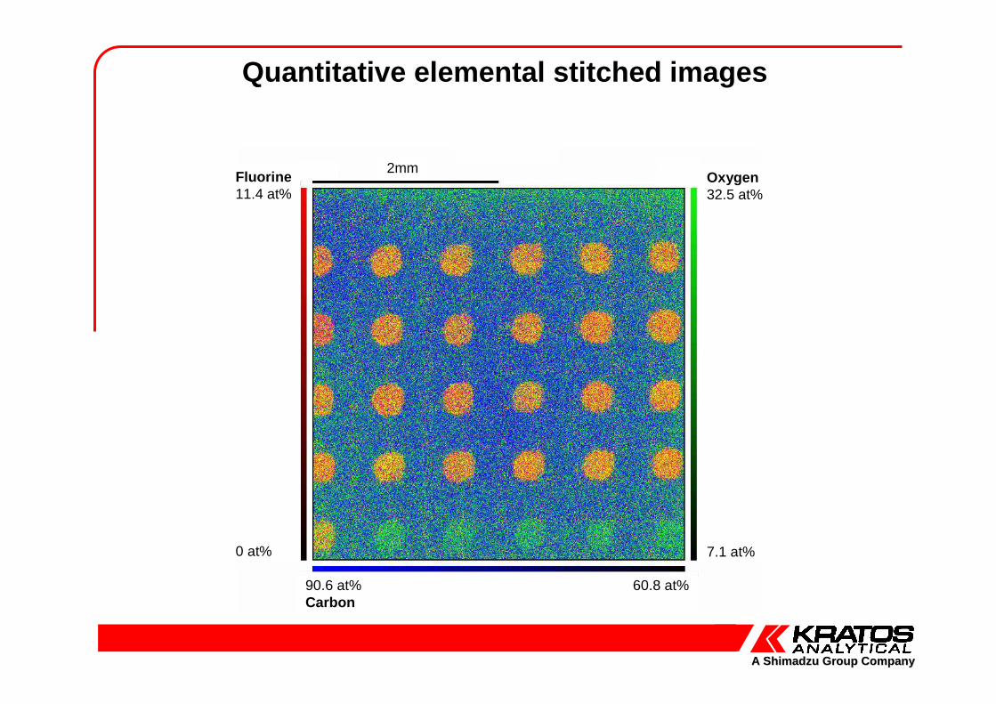
Quantitative elemental stitched images
Fluorine11.4 at%
0 at%
90.6 at% 60.8 at%Carbon
Oxygen32.5 at%
7.1 at%
2mm
A Shimadzu Group CompanyA Shimadzu Group Company
Extending 2D information into 3D
• Several methods available for extending the top surface information into 3D
– Sputter depth profiling• Most common method used
• Utilizes either inorganic or organic molecules as the sputtering agent– Ar ions are typically used for inorganic materials– Organic molecules such as Coronene or C60 are used for organic
materials
• This method enables nanometer information to be extended to 100’s of nm’s or even into the µm range
– Mechanical methods• Not precise but can be used to investigate large depths
A Shimadzu Group CompanyA Shimadzu Group Company
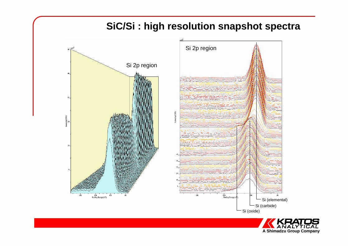
Si 2p region
Si (elemental)
Si (carbide)Si (oxide)
Si 2p region
SiC/Si : high resolution snapshot spectra
A Shimadzu Group CompanyA Shimadzu Group Company
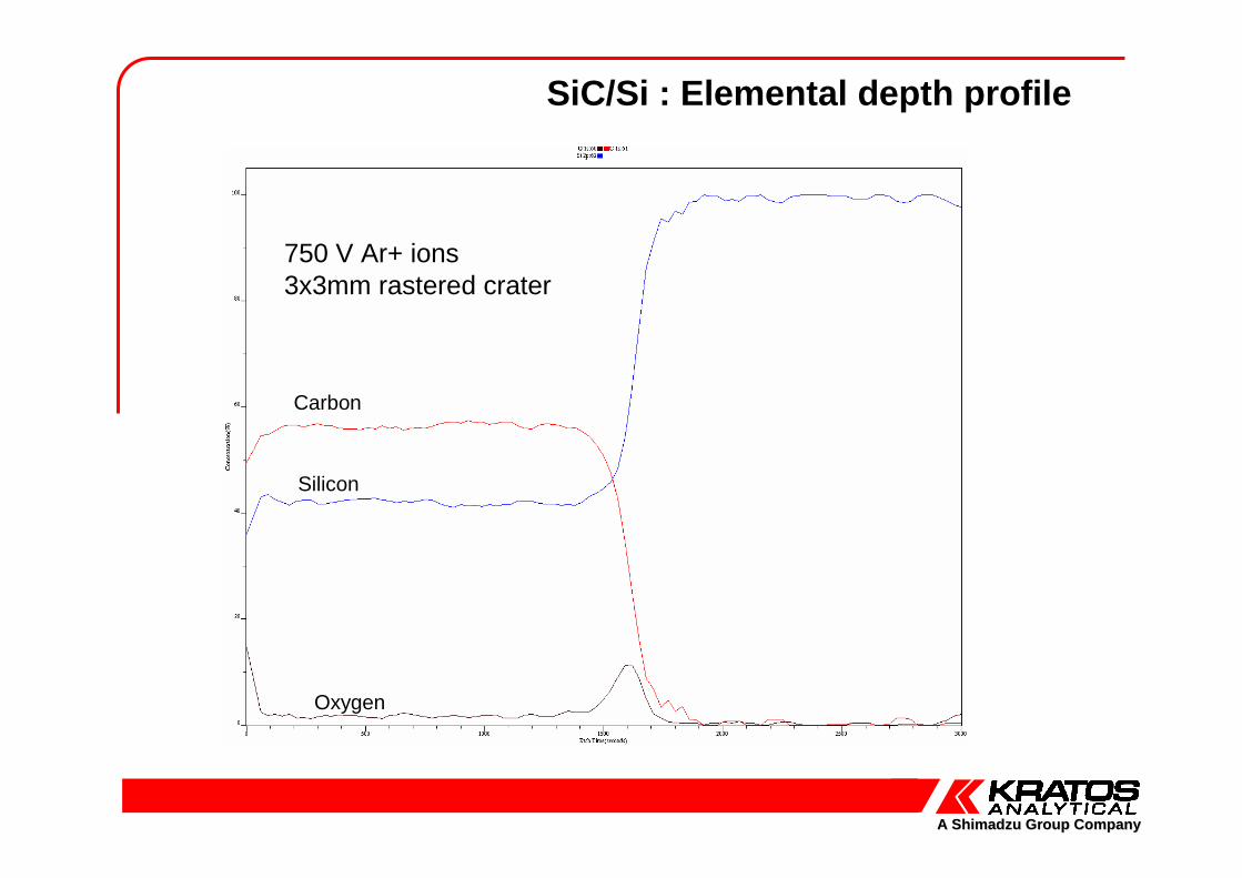
SiC/Si : Elemental depth profile
Oxygen
Silicon
Carbon
750 V Ar+ ions3x3mm rastered crater
A Shimadzu Group CompanyA Shimadzu Group Company
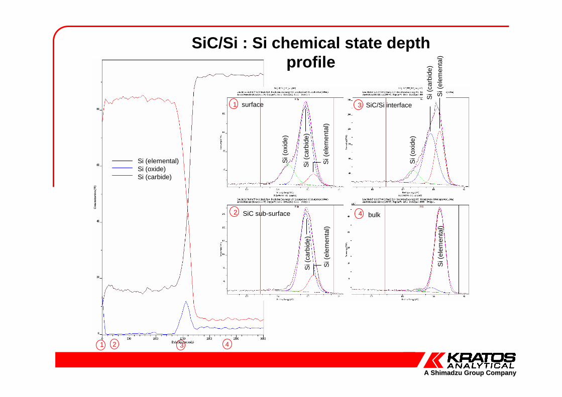
SiC/Si : Si chemical state depth profile
Si (
elem
enta
l)
Si (
carb
ide)
Si (
oxid
e)
Si (
elem
enta
l)
Si (
carb
ide)
Si (
oxid
e)
Si (
elem
enta
l)
Si (
elem
enta
l)
Si (
carb
ide)
2 41 3
1
2
3
4
Si (elemental)Si (oxide)Si (carbide)
surface
bulk
SiC/Si interface
SiC sub-surface
A Shimadzu Group CompanyA Shimadzu Group Company
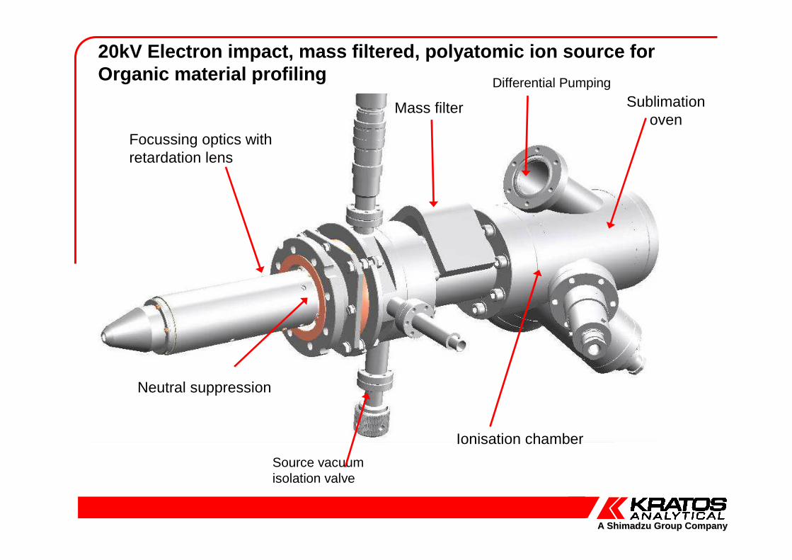
20kV Electron impact, mass filtered, polyatomic ion source for Organic material profiling
Mass filter
Focussing optics with retardation lens
Source vacuum isolation valve
Ionisation chamber
Differential Pumping
Sublimation oven
Neutral suppression
A Shimadzu Group CompanyA Shimadzu Group Company
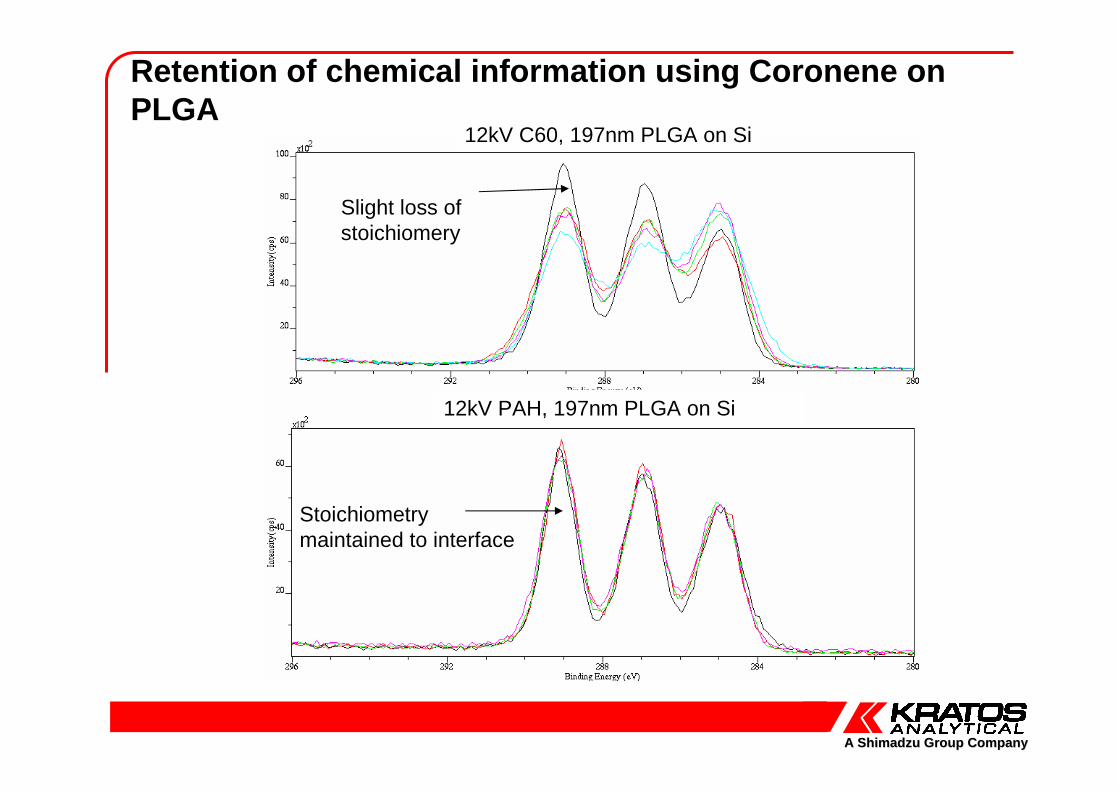
12kV PAH, 197nm PLGA on Si
12kV C60, 197nm PLGA on Si
Retention of chemical information using Coronene on PLGA
Slight loss of stoichiomery
Stoichiometrymaintained to interface
A Shimadzu Group CompanyA Shimadzu Group Company
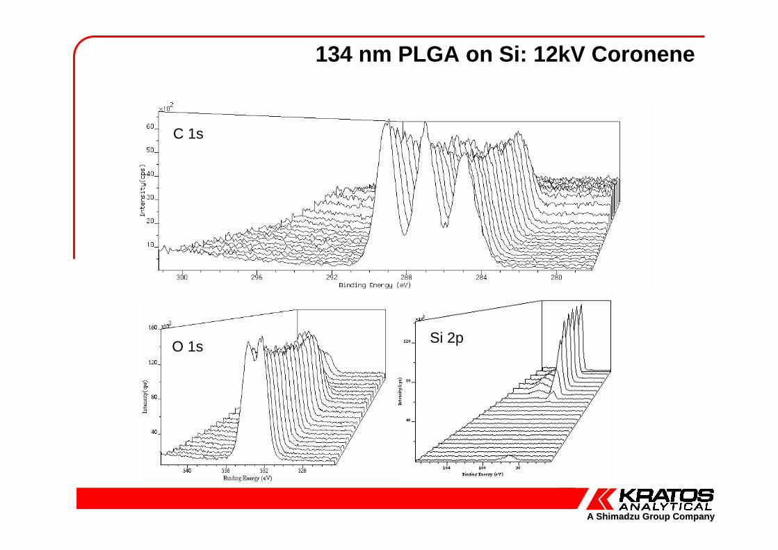
134 nm PLGA on Si: 12kV Coronene
C 1s
O 1sSi 2p
A Shimadzu Group CompanyA Shimadzu Group Company
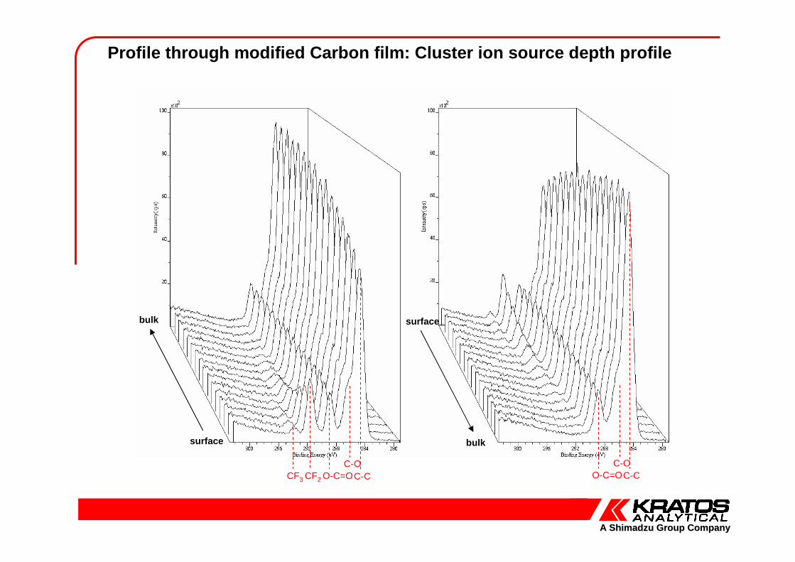
Profile through modified Carbon film: Cluster ion s ource depth profile
surface
bulk
bulk
surface
CF3 CF2 O-C=OC-O
C-C O-C=OC-O
C-C
A Shimadzu Group CompanyA Shimadzu Group Company
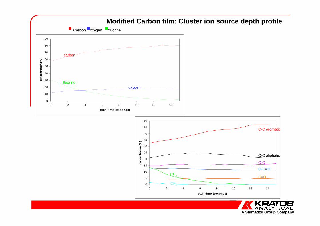
Modified Carbon film: Cluster ion source depth prof ile
0
10
20
30
40
50
60
70
80
90
0 2 4 6 8 10 12 14
etch time (seconds)
conc
entra
tion
(%)
carbon
oxygenfluorine
Carbon oxygen fluorine
0
5
10
15
20
25
30
35
40
45
50
0 2 4 6 8 10 12 14
etch time (seconds)
conc
entra
tion
(%)
C-C aromatic
C-C aliphatic
C-O
O-C=O
C=OCF2
CF3
A Shimadzu Group CompanyA Shimadzu Group Company
Conclusions
• XPS is an ideal technique for the investigation of material surfaces providing information on the nanometer scale
– It provides elemental information– Chemical information– Quantitative information– Detection levels on the order of 1ppb (cf bulk analysis techniques)– Spatially resolved information at the micron level
• Quantitative imaging
– 3D distributions of both elements and chemical states• Use of Polyatomic species enhances organic material information

A Shimadzu Group CompanyA Shimadzu Group Company
Acknowledgements
• All my colleagues at Kratos Analytical for their contributions both to this talk and the continued development of the instrumentation that makes this all possible.
• Neil Fairley – CASA XPS
• Dr. Morgan Alexander – Nottingham University, UK
• Dr. Alex Shard – NPL, Teddington, UK