Reliability improvement of InGaZnO thin film transistors ...

Lateral And Vertical Organic Thin Film Transistors
1
LATERAL AND VERTICAL
ORGANIC THIN FILM
TRANSISTORS
Research Thesis
Submitted in Partial Fulfilment of The Requirements for the Degree of
Master of Science
Oded Globerman
Submitted to the Senate of the Technion-Israel Institute of technology
Nisan 5766 HAIFA April 2006

Lateral And Vertical Organic Thin Film Transistors
2
The research thesis was done under the supervision of Prof. Nir Tessler in electrical
engineering faculty in the Technion.
I wish to express my deepest respect to Prof. Nir Tessler, for his devoted supervision.
I thank Prof. Nir Tessler for introducing me with the field of organic and polymer
electronics.
I thank PhD. Roy Shenhar for his contribution to this thesis, by exposing the exciting
field of block co-polymer, and for spending long hours at the organic lab.
I wish to thank Vlad Medevdev, Yair Gannot, Dr. Olga Solomeshch and Alexey
Razin for the great help in the organic lab.
I thank my colleagues, Noam Rapaport, Yhoram Bar, Michal Soreni and Evgeni
Preezant for the assistance through this thesis.
Neta, my wonderful wife, I wish to thank you for your love and support in the last
four years. I wish to thank my dear parents, Yossef and Rayia, my sister and brother,
Nechama and Israel, and all the family for their love and support.
Lateral And Vertical Organic Thin Film Transistors
3
Contents List of figures ................................................................................................................................................................ 6
List of tables .................................................................................................................................................................. 9
Abstract ......................................................................................................................................................................... 1
List of Symbols ............................................................................................................................................................. 2
1. INTRODUCTION ................................................................................................................................................... 5
1.1 Organic Thin Film Transistor OTFT .................................................................................................................. 5
1.2 C60 Buckminster-Fullerene ................................................................................................................................... 8
1.3 Organization of Thesis ........................................................................................................................................ 10
2. ELECTRONIC STRUCTURE OF ORGANIC MATERIALS ........................................................................ 11
2.1 Introduction .......................................................................................................................................................... 11
2.2 SP2 bonding of Carbon atoms ............................................................................................................................ 12
2.3 2D Carbon Chain (Benzene Ring) ..................................................................................................................... 14
2.4 Small Organic molecule (C60) ............................................................................................................................. 16
2.5 Molecular vibrations ........................................................................................................................................... 17
2.6 Electronics excited states ..................................................................................................................................... 18
2.7 Charge transfer in small organic molecular ..................................................................................................... 20
2.7.1 Intra site transfer (inside the organic molecular) .......................................................................................... 20
2.7.2 Inter site transfer (between organic molecules) ............................................................................................ 20
2.8 Metal Organic Semiconductor Contact ............................................................................................................. 23
2.8.1 Work function Model .................................................................................................................................... 23
2.8.2 Ohmic Contact ............................................................................................................................................... 27
2.8.3 Schottky Contact ........................................................................................................................................... 29
3. LATERAL THIN FILM TRANSISTOR ............................................................................................................ 35
3.1 introductions ......................................................................................................................................................... 35
3.2 Lateral OTFT structure ...................................................................................................................................... 36
3.3 C60 OTFT – literature survey ............................................................................................................................. 38
3.4 Metal Oxide Semiconductor Capacitor ............................................................................................................. 41

Lateral And Vertical Organic Thin Film Transistors
4
3.4.1 Flat band ........................................................................................................................................................ 42
3.4.2 Depletion Mode & Inversion Mode .............................................................................................................. 45
3.4.3 Accumulation Mode ...................................................................................................................................... 47
3.5 Lateral Metal Oxide Semiconductor TFT ......................................................................................................... 48
3.5.1 Current Voltage relationship ......................................................................................................................... 48
3.5.2 Equivalent circuit ........................................................................................................................................... 52
3.5.3 Threshold Voltage ......................................................................................................................................... 54
3.5.4 Trap Effect ..................................................................................................................................................... 57
3.5.5 Mobility ......................................................................................................................................................... 58
4. LATERAL OTFT PROCESSING & CHARACTERIZATION ...................................................................... 61
4.1 introduction .......................................................................................................................................................... 61
4.2 Device processing ................................................................................................................................................. 62
4.2.1 Silicon platform ............................................................................................................................................. 62
4.2.2 C60 Organic Semiconductor Evaporation ...................................................................................................... 63
4.2.3 Metal Top Contact Evaporation .................................................................................................................... 64
4.3 Measurements and Characterizations ............................................................................................................... 66
4.3.1 Measurement techniques ............................................................................................................................... 66
4.4 Lateral OTFT I-V Characterization .................................................................................................................. 68
4.4.1 Ids – Vds characteristic .................................................................................................................................... 68
4.4.2 Ids - Vgs characteristic .................................................................................................................................... 70
4.4.3 Threshold Voltage & Effective Mobility ...................................................................................................... 76
4.5 Contact Effect on Threshold Voltage & Effective Mobility ............................................................................ 80
4.5.1 Contact Effect (Ag, Cu, Au) .......................................................................................................................... 80
4.5.2 Ids - Vds characteristic .................................................................................................................................... 81
4.5.3 Threshold Voltage & Effective Mobility ...................................................................................................... 83
4.6 scanning probe micrograph (SEM) images ....................................................................................................... 86
4.7 Summary ............................................................................................................................................................... 88
5. NOVEL VERTICAL ORGANIC THIN FILM TRANSISTOR ...................................................................... 91
5.1 introduction .......................................................................................................................................................... 91
5.2 Vertical OTFT ...................................................................................................................................................... 92

Lateral And Vertical Organic Thin Film Transistors
5
5.2.1 Benefit of Vertical TFT ................................................................................................................................. 92
5.2.2 Vertical OTFT in literature ........................................................................................................................... 92
5.3 Patterned Source Vertical Organic Thin Film Transistor ............................................................................ 101
5.3.1 Block Co Polymers (BCP) .......................................................................................................................... 101
5.3.2 PS-VOTFT Structure ................................................................................................................................... 104
5.3.3 Patterned Source electrode .......................................................................................................................... 105
5.4 Work function model ......................................................................................................................................... 108
5.5 Two dimension Poisson’s equation simulation ............................................................................................... 111
5.6 Equivalent circuit ............................................................................................................................................... 114
5.7 Schottky Contact Effect .................................................................................................................................... 115
6. PS-VOTFT PROCESSING & CHARACTERIZATION .............................................................................. 117
6.1 introduction ........................................................................................................................................................ 117
6.2 Device processing ............................................................................................................................................... 118
6.2.1 Block Co-Polymer layer .............................................................................................................................. 118
6.2.2 Metal Source Evaporation ........................................................................................................................... 119
6.2.3 C60 Organic Semiconductor Evaporation ................................................................................................... 121
6.2.4 Metal Top Contact Evaporation .................................................................................................................. 121
6.2.5 Buffer lithium fluoride (LIF) layer Evaporation ........................................................................................ 122
6.3 PS-VOTFT I-V Characterization .................................................................................................................... 124
6.3.1 I- Vds ............................................................................................................................................................ 124
6.3.2 I- Vgs ............................................................................................................................................................ 128
6.4 Summary ............................................................................................................................................................. 130
7. SUMMARY & FUTURE WORK ...................................................................................................................... 131
7.1 Summary ............................................................................................................................................................. 131
7.2 Future Work ....................................................................................................................................................... 132
8. REFERENCE ....................................................................................................................................................... 133

Lateral And Vertical Organic Thin Film Transistors
6
List of figures
Figure 1: Organic and polymer electronics product ...................................................................................................... 5
Figure 2: Mobility of N-type and P-type organic and polymers TFT devices [69] ...................................................... 6
Figure 3: Structure of C60 molecule with 60 carbon atoms .......................................................................................... 8
Figure 4: Single C60 molecule Transistor reported by H. Park et al. [41] ..................................................................... 9
Figure 5: Two carbon atoms with SP2 orbital ............................................................................................................. 12
Figure 6: Coupling of degenerate SP2 ......................................................................................................................... 13
Figure 7: Ring of six carbon atoms creating the benzene ring.. .................................................................................. 14
Figure 8: Benzene ring energetically-different orbital. ............................................................................................... 15
Figure 9: Structure of C60 football molecule with Double and single bond. [45]. ..................................................... 16
Figure 10: Absorption process between the electronic ground state and first excited state. ...................................... 18
Figure 11: Absorption and emission spectrum of two electronic state. ...................................................................... 19
Figure 12: Stable and unstabl Pyracylene C60 unit [49]. ............................................................................................. 20
Figure 13: localized energy levels site [54]. ................................................................................................................ 21
Figure 14: Hopping probability versus energy changes between two tied sites [54] ................................................. 22
Figure 15: Partly empty valence band and partly full conductive band.. ................................................................... 23
Figure 16: Fermi-Dirac distribution function. ............................................................................................................. 24
Figure 17: Fermi-Dirac distribution function [54]. .................................................................................................... 25
Figure 18: Intrinsic Semiconductor energy levels. ...................................................................................................... 25
Figure 19: Doped semiconductor energy levels .......................................................................................................... 26
Figure 20: Metal, semiconductor and insulator energy levels and work function ...................................................... 26
Figure 21: Ohmic contact between Low work function metal,and organic LUMO level ........................................ 28
Figure 22: Schottky contact phenomenon ................................................................................................................... 29
Figure 23: lowering of the contact barrier [57]. ......................................................................................................... 30
Figure 24: Schottky barrier lowering φΔ by applying reverse electric field [57]. ................................................. 33
Figure 25: Top gate lateral FET [56]. .......................................................................................................................... 36
Figure 26: Bottom gate coplanar OTFT. ..................................................................................................................... 36
Figure 27: Bottom gate staggered OTFT. .................................................................................................................... 37
Figure 28: Two types of synthesis soluble C60 materials for OTFT devices. [69] [68]. ............................................ 39
Figure 29: Channel negative charges induced by the gate potential .......................................................................... 41
Figure 30: Metal, insulator and semiconductor energy levels before physical contact [56]. ..................................... 42
Figure 31: Fermi level alignment and the energy levels bending of the semiconductor at equilibrium state............ 42

Lateral And Vertical Organic Thin Film Transistors
7
Figure 32: Flat band conditions ................................................................................................................................... 45
Figure 33: Depletion mode .......................................................................................................................................... 45
Figure 34: Inversion mode ........................................................................................................................................... 46
Figure 35: Accumulation mode. .................................................................................................................................. 47
Figure 36: Conductance characteristic for thin film transistor [56]. ........................................................................... 51
Figure 37: Equivalent circuit for lateral staggered OTFT device. .............................................................................. 52
Figure 38: Different view of figure 37. ....................................................................................................................... 52
Figure 39: DH4T OTFT [72]. ...................................................................................................................................... 53
Figure 40: Channel resistance and total resistance for staggered Pentacene TFT [73]. ............................................. 54
Figure 41: Calculated potential distribution at the channel interface [97]. ................................................................ 56
Figure 42: Threshold voltage increase with Pentacene thickness[74]. ....................................................................... 56
Figure 43: Trap’s state located at the insulator-semiconductor interface filled by Fermi level rises [77]. ............... 57
Figure 44: Schematic of the evaporation chamber ...................................................................................................... 63
Figure 45: Picture of doped Si/SiO2 wafer after C60 thermal evaporation ................................................................. 64
Figure 46: Picture of lateral C60 OTFT ....................................................................................................................... 65
Figure 47: OTFT measurements setup. ....................................................................................................................... 66
Figure 48: Scanning probe micrograph (SPM). .......................................................................................................... 67
Figure 49: Conductance characteristic for C60 OTFT ................................................................................................. 68
Figure 50: Logarithmic linear conductance characteristic for C60 OTFT. .................................................................. 69
Figure 51: Transconductance characteristic for C60 OTFT ......................................................................................... 70
Figure 52: Logarithmic linear transconductance characteristic for C60 OTFT ........................................................... 71
Figure 53: Contact, channel and total transistor resistance for constant drain-source voltage Vds=2[V]. ................. 73
Figure 54: Contact, channel and total transistor resistance for constant gate-source voltage Vgs=12[V]. ................ 74
Figure 55: Fitting equation 4.4, 3.25 to part of the logarithmic linear conductance characteristic .......................... 75
Figure 56: Threshold voltage for C60 OTFT ............................................................................................................... 76
Figure 57: Effective mobility factor dependence on drain-source voltage for C60 OTFT ......................................... 77
Figure 58: Effective saturation mobility value dependence on gate-source voltage. ................................................ 78
Figure 59: Effective linear mobility value dependence on gate-source voltage. ........................................................ 78
Figure 60: Work function model of metal contacts and C60 semiconductor before real contact ............................... 81
Figure 61: Conductance characteristic for C60 OTFT with silicon dioxide and silver , copper or gold contacts. ..... 82
Figure 62: Comparison between silver, copper or gold contact C60 OTFT ................................................................ 83
Figure 63: Threshold voltage for C60 OTFT with silicon dioxide insulator and silver , copper or gold contacts .... 84
Figure 64: Effective mobility factor dependence on gate-source voltage for silver, copper or gold contacts. ......... 85

Lateral And Vertical Organic Thin Film Transistors
8
Figure 65: SPM scan for Si/SiO2/block-copolymer/ C60 (~10[nm]). .......................................................................... 87
Figure 66: SPM scan for Si/SiO2/ C60 (~10[nm]) ........................................................................................................ 87
Figure 67: Fabrication steps for the self-aligned vertical channel polymer FET [30] ................................................ 93
Figure 68: Conductance characteristics for F8T2 self-aligned vertical channel polymer FET [30] .......................... 94
Figure 69: Conductance characteristics for P3HT self-aligned vertical channel polymer FET [30] ......................... 94
Figure 70: Parashkov Vertical-channel fabrication process [86] ................................................................................ 95
Figure 71: Parashkov Vertical-channel Conductance and transconductance characteristics [86]. ............................ 95
Figure 72: Kudo et. al. Static induction transistor (SIT) structure [87] ...................................................................... 96
Figure 73: SIT energy band diagram [32] ................................................................................................................... 97
Figure 74: SIT conductance characteristics [32]. ........................................................................................................ 97
Figure 75: Nakayama et. al. charge injection controlled transistor (CICT) structure [90] ......................................... 98
Figure 76: CICT collector current and current amplification factor (hFE) [90]. ........................................................ 98
Figure 77: Ma et. al. gate-source-drain vertical organic field effect transistor (VOFET) [33] .................................. 99
Figure 78: VOFET band diagram [33] ........................................................................................................................ 99
Figure 79: VOFET conductance characteristicse [33] .............................................................................................. 100
Figure 80: OLED driven by the VOFET device [33] ................................................................................................ 100
Figure 81: Chemical structure for donor-acceptor diblolck copolymer PPV-b-P(S-stat- C60MS) [94]. .................. 101
Figure 82: Structural 3D pattern of block copolymer [100]...................................................................................... 102
Figure 83: Block copolymer boundary conditions influence by film thickness [102] ............................................. 103
Figure 84: PS-b-PMMA of the proposed novel patterned source vertical OTFT (PS-VOTFT) .............................. 104
Figure 85: PS-b-PMMA Block copolymer transmission electron microscopy (TEM) [103] .................................. 106
Figure 86: Metal nano particles formation on PS-b-PMMA at different stages [103] ............................................. 107
Figure 87: Work function model for separated silver and C60 .................................................................................. 108
Figure 88: Work function model after thermal equilibrium ...................................................................................... 109
Figure 89: Work function model after applying external voltage ............................................................................. 109
Figure 90: Work function model after applying gate voltage ................................................................................... 110
Figure 91: PS-VOTFT Poisson’s equation simulation Vgs=0[V] and Vds=5[V] ...................................................... 111
Figure 92: Potential and electric field across the source layer when Vg=0[V] ........................................................ 112
Figure 93: PS-VOTFT Poisson’s equation simulation with Vgs=5[V] and Vds=5[V] .............................................. 112
Figure 94: Potential and electric field across the source layer when Vg=5[V ........................................................ 113
Figure 95: PS-VOTFT Poisson’s equation simulation comparison between Vgs=0[V] and Vgs=5[V] ................... 113
Figure 96: PS-VOTFT Equivalent circuit ................................................................................................................. 114
Figure 97: A scanning probe micrograph imaging of PS-b-PMMA block copolymer template ............................. 118

Lateral And Vertical Organic Thin Film Transistors
9
Figure 98: A scanning electron micrograph (SEM) image of ~10[nm] thick silver nano-scale particles. .............. 120
Figure 99: A scanning electron micrograph (SEM) image of ~20 [nm] thick silver nano-scale conductive grids . 121
Figure 100: PS-VOTFT image. ................................................................................................................................. 122
Figure 101: PS-VOTFT I-V semi-logarithmic curve ............................................................................................... 124
Figure 102: Conductance characteristic for PS-VOTFT device. .............................................................................. 126
Figure 103: Semi-logarithmic conductance characteristic for PS-VOTFT device ................................................... 127
Figure 104: PS-VOTFT transconductance characteristic.. ....................................................................................... 128
Figure 105: A semi logarithmic fit to the PS-VOTFT transconductance characteristic. ......................................... 129
List of tables Table 1: Threshold voltage and saturated effective mobility values for silver contacts SiO2/BCP insulator
transistor………………………………………….…………………………………………………………………79
Table 2: Threshold voltage and saturated effective mobility values for silver, copper and gold contacts SiO2
insulator transistor. …………………………………...…………………………………………………………….85
Table 3: Summary of lateral transistors shown in this thesis…………………………………………….89
Table 4: m1 and m2 Coefficient from figure 103, according to equation 6.4.………………………………..….….127


Lateral And Vertical Organic Thin Film Transistors
1
Abstract
Organic and polymer electronics have been the subject of intense research for the
past 30 years, after the discovery of Heeger, MacDiarmid and Shirakawa, that
polyacetylene can be rendered conductive by reaction with bromine or Iodine
vapours. At the year 2000 when Heeger, MacDiarmid and Shirakawa were granted the
Nobel prize in Chemistry for foundering of the “conjugated polymer science” few
organic electronics products have emerged in the market, first as organic or polymer
display (OLED and PLED) and recently as organic or polymer transistors (OTFT or
PTFT). Future applications promise large area flexible organic flat display, derived by
active matrix organic transistors (AM-OTFT). To realize this idea there is a need to
boost the performance of today organic transistor by few factors.
This thesis was aimed to research the effect of structural and materials on the
performance of OTFT. We chose to use C60 “Bucky Ball” as the active semiconductor
material throughout the research. We first inspected the effect of using different
contacts and insulator material upon the performance of “standard “ lateral OTFT
structure.
The second part of the thesis, deals with novel vertical transistor structure, which
target to increase the device performance. In order to implement the proposed vertical
structure we needed to be exposed to the new science of nano scale patterning based
on block co-polymer (BCP) materials. This technology enables us to assemble and
demonstrate the PS-VOTFT device.

Lateral And Vertical Organic Thin Film Transistors
2
List of Symbols
Symbol Meaning a-Si:H hydrogenated amorphous Silicon
AM-TFT Active Matrix TFT
BCP Block co-polymer
BOC Bottom contact
CICT Charge injection controlled transistor
CMOS Complementary Metal Oxide Semiconductor
CV Capacitance voltage
Cins Insulator capacitance
DOS Density of states
E Electric field
EC Conductance band edge
EF Fermi level
EV Valence band edge
gE Band gap Energy
( ) ( ), ,f fε η ε Distribution function
)(Ef probability to find a charge at energy E
FET Field effect transistor
( )g ε Density of states
HOMO Highest Occupied Molecular Orbital
Ids The drain source current
K Boltzmann coefficient
KPFM Kelvin probe force microscopy
Lch Channel length
LED Light Emitting Diode
LIF Lithium fluoride
Leff The effective channel length
LUMO Lowest Unoccupied Molecular Orbital
MBT Metal base transistor
MEH-PPV Polymethoxy-Ethyl-Hexyloxy-Phenylen-Vinylene
Lateral And Vertical Organic Thin Film Transistors
3
Symbol Meaning MIS Metal Insulator Semiconductor
MOS Metal Oxide Semiconductor
)(En charge density
OLED Organic Light Emitting Diode
OTFT Organic Thin Film Transistor
P Probability vector
p Charge concentration
)(Ep charge density
PS Poly-Styrene
PMMA Poly-Methyl-Meth-Acrylate
PT Poly-Thiophene
PFET Polymer Field Effect Transistor
PS-VOTFT Pattern Source Vertical OTFT
PS-b-PMMA Polystyrene-block-Polymethylmethacrylate
Q Total charge in the channel
q Charge carrier charge, electron charge
Rij State to state distance
RFID Radio Frequency identification Tag
Rtot The transistor total resistance
Rch The channel resistance
Rcon The contact resistance
SIT Static Induction Transistor
T Temperature
Tg Glass transition temperature
tox Oxide width
tins The insulator layer thickness
TFT Thin Film Transistor
TOC Top Contact
TOF Time Of Flight
UHV Ultra High Vacuum
VT Threshold Voltage

Lateral And Vertical Organic Thin Film Transistors
4
Symbol Meaning VOTFT Vertical OTFT
Vgs The gate to source potential
Vds The drain to source potential
Wch Channel width
ε Energy, dielectric constant
oxε Permittivity of oxide
iε Energy of state i
sε Semiconductor permittivity.
oε The free space permittivity
insε The insulator relative permittivity
oiε Permittivity of organic insulator
σ The channel conductivity, Carbon conjugated orbital
μ Mobility
π Carbon conjugated orbital
mΦ Metal work function
Fφ The potential difference between the intrinsic Fermi level and the doped Fermi level
ijυ Transfer rate
χ Electron affinity
Sχ The semiconductor electron affinity
Lateral And Vertical Organic Thin Film Transistors
5
11.. IINNTTRROODDUUCCTTIIOONN
1.1 Organic Thin Film Transistor OTFT
Organic thin film transistors (OTFT) have gained high interest in the last years due
to their potential applications in small as well as in large area electronics. Their less
complex processing procedures, utilizing low temperature deposition and solution
processing methods, hold promise for cheaper, lightweight and flexible products.
The promising applications for OTFT include active matrix drivers for large area
display [1-4], large area sensor matrix [5-8], active matrix drivers for electronics
paper [9-12] and basic element for logic circuit in Radio Frequency Identification
(RFID) tags [13-16].
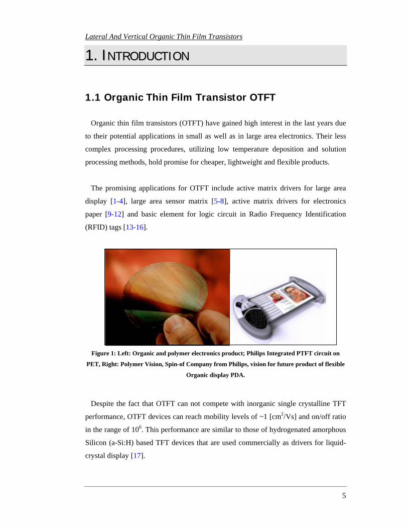
Figure 1: Left: Organic and polymer electronics product; Philips Integrated PTFT circuit on
PET, Right: Polymer Vision, Spin-of Company from Philips, vision for future product of flexible
Organic display PDA.
Despite the fact that OTFT can not compete with inorganic single crystalline TFT
performance, OTFT devices can reach mobility levels of ~1 [cm2/Vs] and on/off ratio
in the range of 106. This performance are similar to those of hydrogenated amorphous
Silicon (a-Si:H) based TFT devices that are used commercially as drivers for liquid-
crystal display [17].
Lateral And Vertical Organic Thin Film Transistors
6
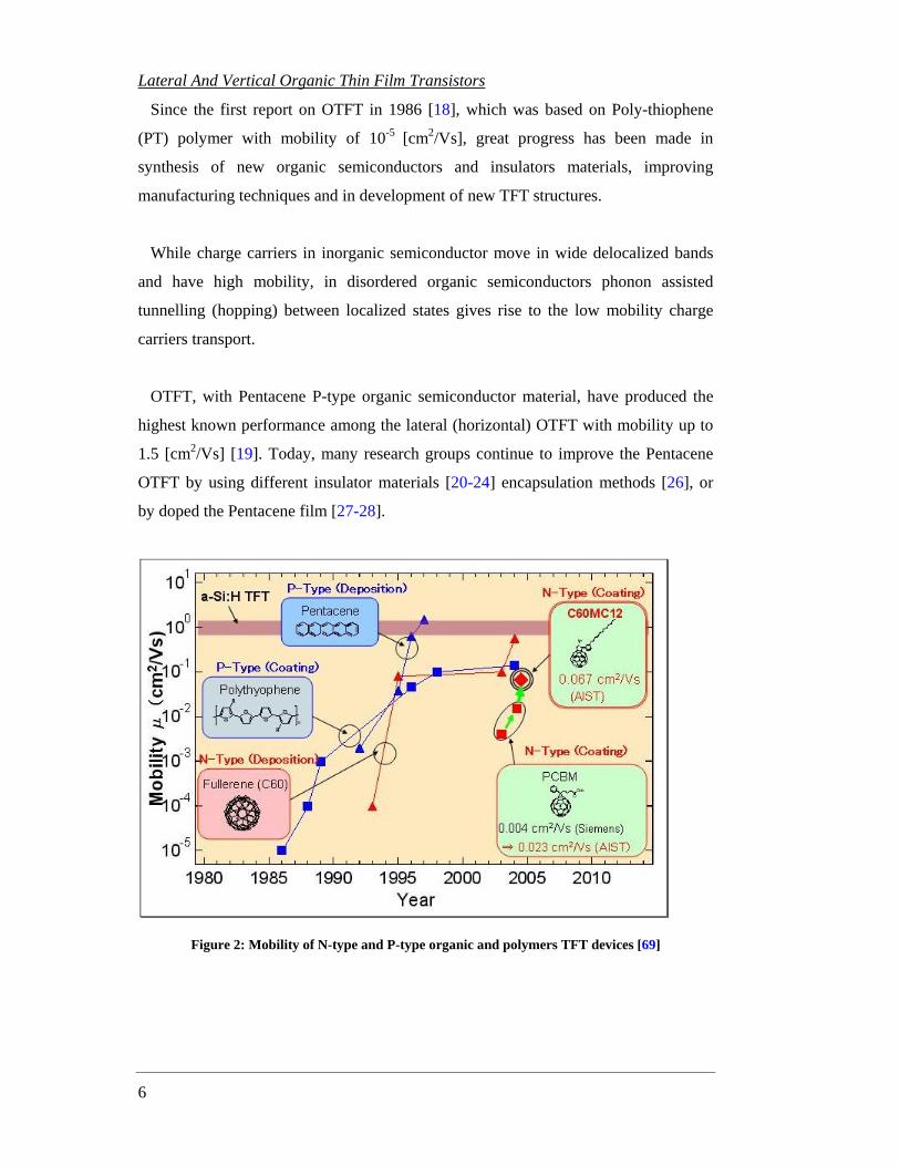
Since the first report on OTFT in 1986 [18], which was based on Poly-thiophene
(PT) polymer with mobility of 10-5 [cm2/Vs], great progress has been made in
synthesis of new organic semiconductors and insulators materials, improving
manufacturing techniques and in development of new TFT structures.
While charge carriers in inorganic semiconductor move in wide delocalized bands
and have high mobility, in disordered organic semiconductors phonon assisted
tunnelling (hopping) between localized states gives rise to the low mobility charge
carriers transport.
OTFT, with Pentacene P-type organic semiconductor material, have produced the
highest known performance among the lateral (horizontal) OTFT with mobility up to
1.5 [cm2/Vs] [19]. Today, many research groups continue to improve the Pentacene
OTFT by using different insulator materials [20-24] encapsulation methods [26], or
by doped the Pentacene film [27-28].
Figure 2: Mobility of N-type and P-type organic and polymers TFT devices [69]

Lateral And Vertical Organic Thin Film Transistors
7
The microscopic mobility upper limits of organic molecular crystal tested by time of
flight experiments at room temperature [29] is between 1 to 10 [cm2/Vs], impose by
the weak intermolecular force between neighbouring molecules. There are also large
efforts in pushing disordered polymers semiconductors, which are inherently more
stable [25], toward the high mobility regime, but values higher then 0.1 seem to be out
of reach at the moment.
Reducing the OTFT micron size channel, which contains large number of
molecules, to Nano size channel, with fewer molecules between the TFT contacts,
may improve the OTFT performance. To reach this target few vertical OTFT
structures were designed with channel length in the nanometre dimension. Among
these structures are V-shape channel OTFT [30], SIT OTFT [31-32] and VOTFT
structure proposed by Liping Ma and Yang Yang [33].
The new VOTFT structure described in [33] provides very short channel length and
extremely large cross sectional area between the source and the drain contacts,
allowing low working voltage (gate voltage in the range of few volts) and high current
output (In the range of milliamp for 0.25 mm2 device area). To reach this superior
performance the VOTFT requires unique structural properties, like very thin and
rough source electrode and high capacitance for the bottom cell capacitor, which in
our opinion is significantly lowering the VOTFT manufacturing yield.
In this thesis we are using the C60 fullerene as an active organic semiconductor
material for lateral OTFT and for novel pattern source vertical OTFT (PS-VOTFT)
structures. The PS-VOTFT includes block co-polymer (BCP) as insulator material
and as pattering layer for the source and drain electrode (more detail in chapter 5)

Lateral And Vertical Organic Thin Film Transistors
8
1.2 C60 Buckminster-Fullerene
In 1985 during a research to understand the absorption spectra of interstellar dust,
which was suspected to be related to some kind of long-chained carbon molecules,
R.E. Smalley, H.W. Kroto, J.R. Heath, S.C. O’Brien and R.F. Carl reported [34] the
discovery of a new carbon structure. The new structure, a closed hollow cage of 60
carbon atoms arranged in SP2 hybrid state (Figure 3 left), become the third known
carbon form after the hard, transparent, insulating diamond form and the soft, black,
conductive graphite form.
This discovery, which was followed by winning of the 1996 Nobel Prize, was given
the name “Buckminster-fullerene” after the architect of the Disney-world dome in
Florida design, using the same geometrical structure (Figure 3 right).
Figure 3: Left: C60 molecule with 60 carbon atoms, Right: and Buckminster Fuller's Dome in
Montreal Expo 1967.
In general, the name “Fullerene” is now used to describe all close cages forms of pure
carbon, having from 20 to 1,000,000 and more (nanotubes) carbon atoms, which is the
largest stable molecule, made of a single element.
Fullerene family in general and C60 in particular, have remarkable interesting
chemical and physical properties, Ranging from superconductivity [35-38] to
ferromagnetism [39]. This material shows promising future application in solar cell
devices. Currently Organic solar cells with C60 are the most efficient Organic solar cells
Lateral And Vertical Organic Thin Film Transistors
9
known today, with power conversion efficiency of 4.25% [40]. In the last decade, few
research groups have published articles on C60 OTFT with mobility up to 0.5 [cm2/Vs].
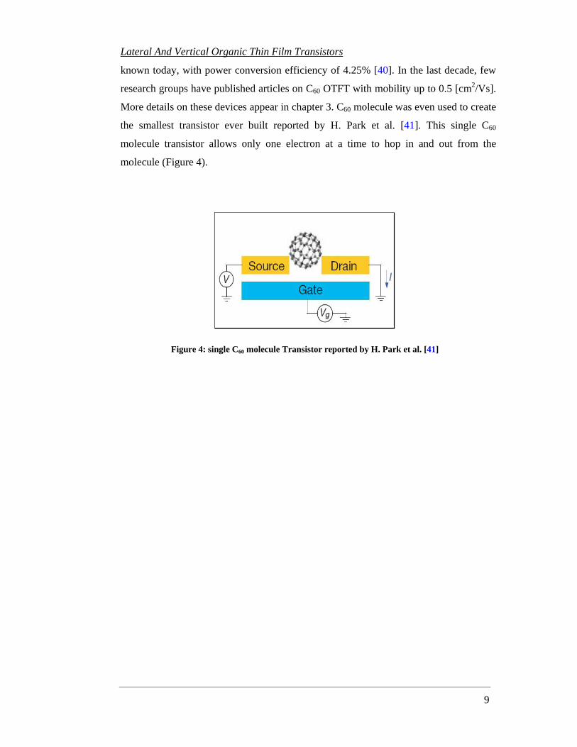
More details on these devices appear in chapter 3. C60 molecule was even used to create
the smallest transistor ever built reported by H. Park et al. [41]. This single C60
molecule transistor allows only one electron at a time to hop in and out from the
molecule (Figure 4).
Figure 4: single C60 molecule Transistor reported by H. Park et al. [41]

Lateral And Vertical Organic Thin Film Transistors
10
1.3 Organization of Thesis Chapter 2 gives general background for SP2 organic conductive materials, with
emphasis on fullerene C60, which we choose as the active semiconductor materials
used throughout this thesis. In addition it deals with two metal semiconductor contact
types, Ohmic and Schottky contacts.
Chapter 3 gives general background for organic thin film transistor (OTFT). This
chapter focuses on C60 OTFT, and includes literature survey for published C60 OTFT.
The basic TFT principles are discusses and the definitions for threshold voltage, trap
effect and effective mobility coefficient are explained.
Chapter 4 shows fabrication process of lateral C60 organic TFT. We characterize the
current-voltage response, the threshold voltage, and the effective mobility value. In
the second part of the chapter, we characterize the performance of different contact
types OTFT. We use a work function model to explain the performance variation.
Chapter 5 discusses the benefit of vertical OTFT compared to lateral OTFT and
relevant published contributions by other groups are presented. In the second part of
the chapter, we deal with the Basic theory for the PS-OVTFT operation, and discuss
the technology that utilize block co-polymer.
Chapter 6 discusses the fabrication process of vertical PS-OTFT. It deals with the
nano pattering of the source electrode and the deposited steps of this device. It shows
the characterize current-voltage measurements. In this chapter we are demonstrating
the idea of PS-OVTFT, and the effect of the gate electric field on the drain-source
current.
Chapter 7 Summary and future work.

Lateral And Vertical Organic Thin Film Transistors
11
22.. EELLEECCTTRROONNIICC SSTTRRUUCCTTUURREE OOFF OORRGGAANNIICC
MMAATTEERRIIAALLSS
2.1 Introduction
This chapter gives general background for SP2 organic conductive
materials, with emphasis on Buckminster- fullerene (C60), which we
choose as the active semiconductor material used during this thesis.
Two types of metal-semiconductor contacts, Ohmic and Schottky, are
discussed.

Lateral And Vertical Organic Thin Film Transistors
12
2.2 SP2 bonding of Carbon atom
Carbon atom with six electrons has electronic configuration of 1S22S22P2. Carbon can
bond with other atoms via hybridization of the outer four 2S and 2P state electrons. In
conjugated materials SP2 hybridization between neighbouring atoms is formed, where 2S,
2Px and 2Py orbital are combined in trigonal planar formation. This strong covalent bond
is called a Sigma (σ ) bond, which forms the backbone of the chain. Electrons in this
orbital are highly localized between the atoms. The energy differences between the low
energy (σ ) state and the excited ( *σ ) state is quite large and well beyond the visible
spectral range. Thus the electronic properties associated with this bond are that of an
insulating material.
The fourth orbital (2Pz) does not take part in this hybridization and is perpendicular to
the σ bond. Neighbouring atoms with 2PZ orbital form together molecular PAI (π )
orbital. Electrons in this bond are less localized to the carbon atoms and more mobile
(figure 5).
Figure 5: Two carbon atoms with SP2 orbital, σ and π bonds. The σ bonds appear in the x-y
plane while π bond appears in Z plane.
The coupling of two degenerate 2Pz orbitals generates two new energetically-different
orbitals: bonding (π - or π ) which is lower in energy compare to original 2Pz orbital,
and anti-bonding (π + or π *) which is higher in energy compared to the isolated 2Pz
orbital (figure 6). Because of the lower energy of the bonding (π -) orbital both of the

Lateral And Vertical Organic Thin Film Transistors
13
2Pz electrons will occupy this orbital, leaving the anti bonding (π +) orbital empty of
electrons. This can be seen in figure 6.
Figure 6: coupling of degenerate SP2 and Pz orbital generates new energetically-different orbital
σ - , σ +, π - and π +. The electrons occupy the lower energy bonding orbital while leaving
the high energy anti boding orbital free of charges.
In this case the bonding orbital is the highest energy occupied molecular orbital
(HOMO), while the anti bonding orbital is the lowest unoccupied molecular orbital
(LUMO). In addition, the energy difference between the π - orbital and π + orbital is
much smaller compared to the energy difference of σ coupling. This band gap has
absorption in the visible range and the delocalized nature of the π orbital leads to
semiconductor properties.
Lateral And Vertical Organic Thin Film Transistors
14
2.3 2D Carbon Chain (Benzene Ring)
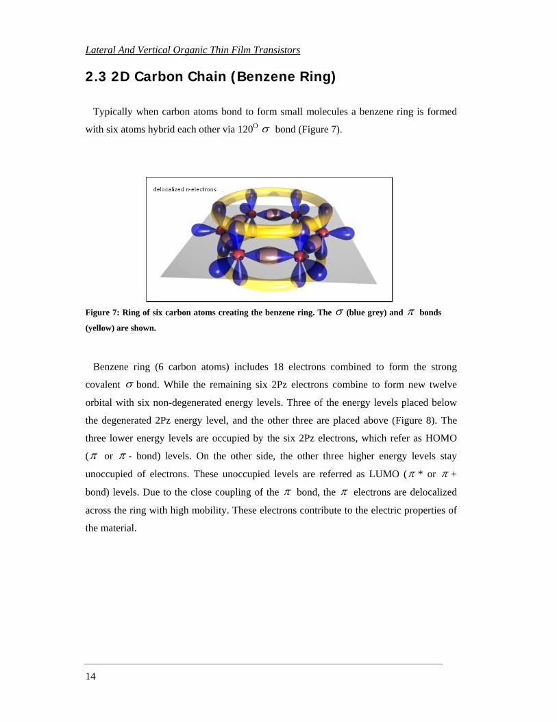
Typically when carbon atoms bond to form small molecules a benzene ring is formed
with six atoms hybrid each other via 120O σ bond (Figure 7).
Figure 7: Ring of six carbon atoms creating the benzene ring. The σ (blue grey) and π bonds
(yellow) are shown.
Benzene ring (6 carbon atoms) includes 18 electrons combined to form the strong
covalent σ bond. While the remaining six 2Pz electrons combine to form new twelve
orbital with six non-degenerated energy levels. Three of the energy levels placed below
the degenerated 2Pz energy level, and the other three are placed above (Figure 8). The
three lower energy levels are occupied by the six 2Pz electrons, which refer as HOMO
(π or π - bond) levels. On the other side, the other three higher energy levels stay
unoccupied of electrons. These unoccupied levels are referred as LUMO (π * or π +
bond) levels. Due to the close coupling of the π bond, the π electrons are delocalized
across the ring with high mobility. These electrons contribute to the electric properties of
the material.

Lateral And Vertical Organic Thin Film Transistors
15
Figure 8: Left up: Schematic view of benzene ring with six junctions, representing carbon and
hydrogen atoms in each junction. Double and single bonds can be seen. Main: benzene ring new
energetically-different orbital crating HOMO level (bonding orbital) and LUMO level (anti-
bonding orbital).
The terms for organic HOMO and LUMO are analogous to valence and conductive
bands used for inorganic solid state physics. According to this analogy electrons or
negative charges are mobile across the LUMO level, while holes or positive charges are
mobile across the HUMO level. Upper left side of figure 8 shows benzene ring format
with single and double bonds. Each edge in the ring defines by carbon atom with
hydrogen atom. Single band (C-C) representing only σ bond, while double bond (C=C)
representing σ bond with π bond.
Lateral And Vertical Organic Thin Film Transistors
16
2.4 Small Organic molecule (C60)
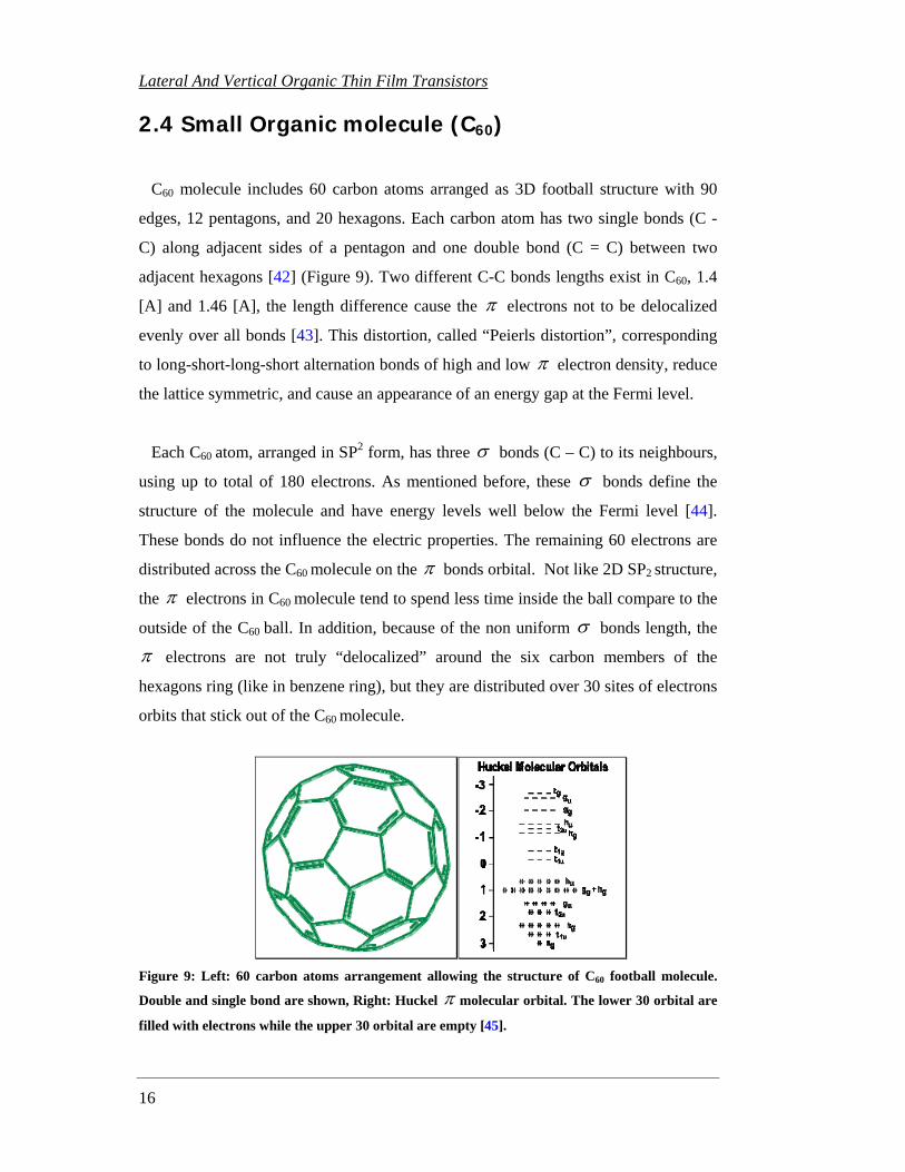
C60 molecule includes 60 carbon atoms arranged as 3D football structure with 90
edges, 12 pentagons, and 20 hexagons. Each carbon atom has two single bonds (C -
C) along adjacent sides of a pentagon and one double bond (C = C) between two
adjacent hexagons [42] (Figure 9). Two different C-C bonds lengths exist in C60, 1.4
[A] and 1.46 [A], the length difference cause the π electrons not to be delocalized
evenly over all bonds [43]. This distortion, called “Peierls distortion”, corresponding
to long-short-long-short alternation bonds of high and low π electron density, reduce
the lattice symmetric, and cause an appearance of an energy gap at the Fermi level.
Each C60 atom, arranged in SP2 form, has three σ bonds (C – C) to its neighbours,
using up to total of 180 electrons. As mentioned before, these σ bonds define the
structure of the molecule and have energy levels well below the Fermi level [44].
These bonds do not influence the electric properties. The remaining 60 electrons are
distributed across the C60 molecule on the π bonds orbital. Not like 2D SP2 structure,
the π electrons in C60 molecule tend to spend less time inside the ball compare to the
outside of the C60 ball. In addition, because of the non uniform σ bonds length, the
π electrons are not truly “delocalized” around the six carbon members of the
hexagons ring (like in benzene ring), but they are distributed over 30 sites of electrons
orbits that stick out of the C60 molecule.
Figure 9: Left: 60 carbon atoms arrangement allowing the structure of C60 football molecule.
Double and single bond are shown, Right: Huckel π molecular orbital. The lower 30 orbital are
filled with electrons while the upper 30 orbital are empty [45].

Lateral And Vertical Organic Thin Film Transistors
17
The order of the π bonds energy level based on Huckel model showed in figure 9
[45]. This model includes 60 orbital with different levels of degeneracy energy. In
which, 30 lower orbital are filled with 60 π electrons. In this case, Hu level is
completely filled by the 10 highest energy electrons, becoming the highest occupied
molecular orbit (HOMO), while the next energy level, t1u, become the lowest
unoccupied molecular orbit (LUMO). This molecular orbit can be partially or fully
filled by injecting electron to the C60 molecule. The HOMO-LUMO band gap is about
2eV to 2.5eV, well inside the visible spectrum and leads to semi conductor properties.
Kelvin probe measurements (KPM) [46, 47] done on C60 film showed that the
electron affinity (the energy needed to pull electron from LUMO level to the vacuum
level) was measured as 3.57 [eV], while the ionization threshold energy (the energy
needed to pull electron from HOMO level to the vacuum level) was measured as 6.17
[eV]. Leading to a HOMO-LUMO band gap of 2.6 [eV].
2.5 Molecular vibrations
Each atom in the C60 molecule can have three vibration modes, leading to a total of
60*3-6=174 intra-molecular vibration mode (-6 sit for the inter-molecule six vibration
modes, when all the molecule’s atoms move at the same direction and phase, three
translational and three rotational). Because of the C60 symmetry a degenerate energy
appears for the intra-molecular vibration. These vibration energies are between
0.03[eV] to 0.2[eV]. In addition, the C60 molecule vibrates and rotates freely. These
inter-molecular motion leads to vibration excitations (Phonons). The phonon energy
are up to ~0.007[eV] [48].This vibration modes excitation are lower by two orders of
magnitude in energy compare to the electron excitation.

Lateral And Vertical Organic Thin Film Transistors
18
2.6 Electronics excited states
While Molecular vibration are excited at the thermal energy spectrum (about
0.007[eV] to 0.2[eV] at room temperature), electronic excitation involve higher
energy, mostly at the visible energy spectrum (about 2[eV] to 2.5[eV]). The electronic
excitation could be created by photons or by charge injection. Figure 10 shows two
discrete electronic levels (ground state and excited state) with supplementary
vibrational energy levels at each electronic level.
Figure 10: Absorption process between the electronic ground state and first excited state. Each
electric state is being assembled by few vibronic states.
When a molecule is excited with photons, fast electronic transitions (~10-15 [Sec])
occur from the ground state to the excited state. This represented by the absorption
process (figure 11 left side). At this point, the system relaxes towards its lowest
vibronic excited state where thermal energy, in the form of molecular vibration or
rotation, is released. From this excited state the system can move to one of the
vibronic excited states of the electronic ground state. This is represented by the
emission process (figure 11 right side).
Lateral And Vertical Organic Thin Film Transistors
19
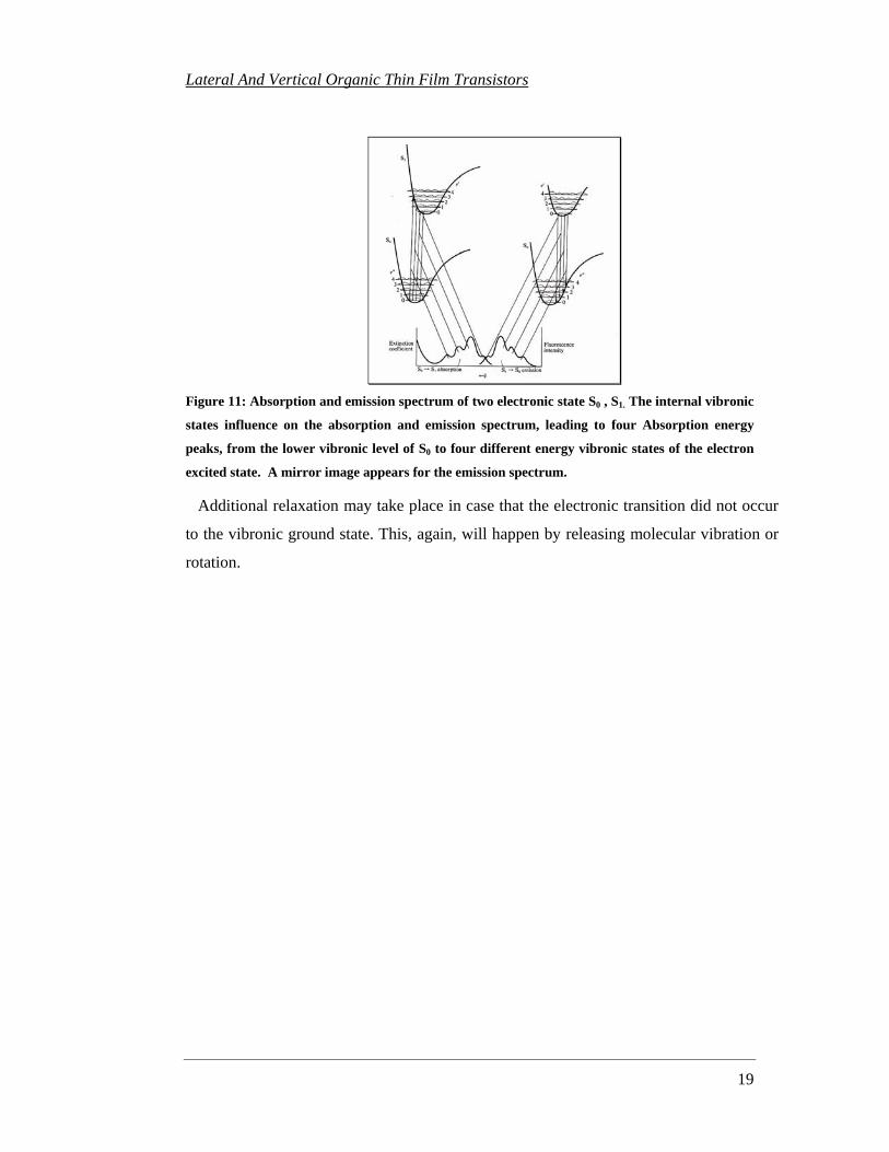
Figure 11: Absorption and emission spectrum of two electronic state S0 , S1. The internal vibronic
states influence on the absorption and emission spectrum, leading to four Absorption energy
peaks, from the lower vibronic level of S0 to four different energy vibronic states of the electron
excited state. A mirror image appears for the emission spectrum.
Additional relaxation may take place in case that the electronic transition did not occur
to the vibronic ground state. This, again, will happen by releasing molecular vibration or
rotation.
Lateral And Vertical Organic Thin Film Transistors
20
2.7 Charge transfer in small organic molecular
2.7.1 Intra site transfer (inside the organic molecular)
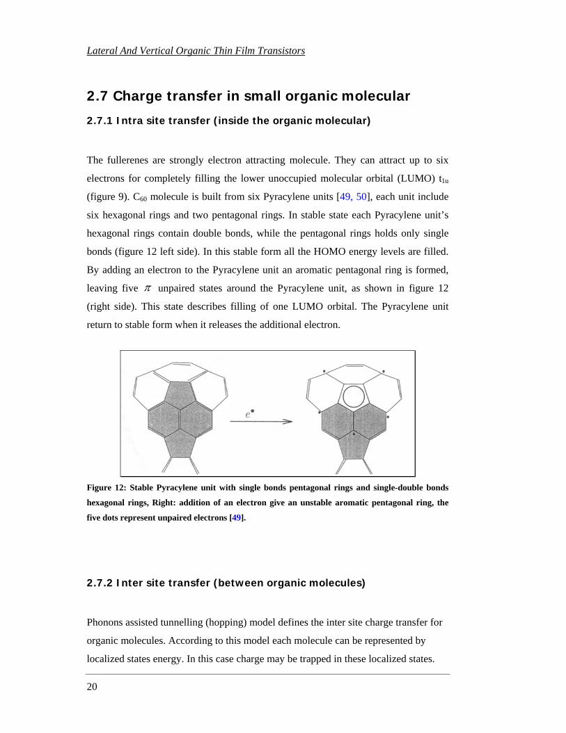
The fullerenes are strongly electron attracting molecule. They can attract up to six
electrons for completely filling the lower unoccupied molecular orbital (LUMO) t1u
(figure 9). C60 molecule is built from six Pyracylene units [49, 50], each unit include
six hexagonal rings and two pentagonal rings. In stable state each Pyracylene unit’s
hexagonal rings contain double bonds, while the pentagonal rings holds only single
bonds (figure 12 left side). In this stable form all the HOMO energy levels are filled.
By adding an electron to the Pyracylene unit an aromatic pentagonal ring is formed,
leaving five π unpaired states around the Pyracylene unit, as shown in figure 12
(right side). This state describes filling of one LUMO orbital. The Pyracylene unit
return to stable form when it releases the additional electron.
Figure 12: Stable Pyracylene unit with single bonds pentagonal rings and single-double bonds
hexagonal rings, Right: addition of an electron give an unstable aromatic pentagonal ring, the
five dots represent unpaired electrons [49].
2.7.2 Inter site transfer (between organic molecules)
Phonons assisted tunnelling (hopping) model defines the inter site charge transfer for
organic molecules. According to this model each molecule can be represented by
localized states energy. In this case charge may be trapped in these localized states.

Lateral And Vertical Organic Thin Film Transistors
21
The amorphous structure nature of organic solids affects the hopping transport [51,
52] mechanism. The charge hopping can be facilitated by molecular thermal
vibration, which changes the relative inter site energy level and assist “trapped”
charge to hop from one localized site to the next localized site.
By applying external electric field across the organic solid the relative localized
energy levels are being shifted. This effect lowers the activation energy (energy
difference between sites) according to the electric field vector, and raises the
probability of charge hopping from traps sites along the field vector. Figure 13 shows
the relative localized inter site energy level for zero and none zero electric field.
x (physical location)
Energy
V=0v
x (physical location)
Energy
V>0v
x (physical location)
Energy
V=0v
x (physical location)
Energy
V=0v
x (physical location)
Energy
V>0v
x (physical location)
Energy
V>0v
Figure 13: localized energy levels site for, Left: zero fields, Right: positive field [54].
Miller and Abrahams proposed hopping model [53] based on single phonon jump
rate (or an effective phonon frequency). In this model the hopping rate depends on the
vibration phonon rate, the tunnelling probability, and the probability of the occupation
level:
⎟⎟⎠
⎞⎜⎜⎝
⎛ −−−=
TkEE
RB
jiijij exp)2exp(0 γνν for ji EE < (2.1)
And: )2exp(0 ijij Rγνν −= for ji EE > (2.2)
Where: ν0 is the vibration phonon rate
)2exp( ijRγ− is the tunnelling probability between two localized energy states
i and j

Lateral And Vertical Organic Thin Film Transistors
22
Rij is the distance between the two sites
γ -1 quantifies the wave function overlap between the sites
⎟⎟⎠
⎞⎜⎜⎝
⎛ −−
TkEE
B
jiexp is the occupation probability of energy difference ji EE −
Left side of figure 14 describes the Miller Abrahams hopping probability
(Frequency) [54]. This figure shows how energy differences jiE effects hoping
probability (with constant vibration phonon rate, wave function, distance and
temperature). It is easy to see, that for situation where the initial energy is higher
compare to the final energy (according to formula 2.2) the hopping probability is
equal to 1.
hoping frequency versus dE
00.20.40.60.8
11.21.4
-0.2 -0.1 0 0.1 0.2
energy change [V]
hopi
ng fr
eque
ncy
Figure 14: Hopping probability versus energy changes between two tied sites [54]; Left:
According to Miller-Abrahams theory, Right: According to Marcus-Mott theory.
There is another form of hopping rate theory which account for the molecular
electron-phonon coupling (Marcus-Mott theory). In this model the transfer of charge
from one molecule to another will occur only when the energy levels are almost
equal, which lead to maximum hopping probability when the energy difference
between two neighbours sites is close to zero energy. Marcus-Mott theory probability
versus energy change appears in the right side of figure 14.
hopping frequency versus dE
0
0.2
0.4
0.6
0.8
1
1.2
-0.05 0 0.05 0.1 0.15 0.2
energy change [V]
hopp
ing
freq
uenc
y
Lateral And Vertical Organic Thin Film Transistors
23
2.8 Metal Organic Semiconductor Contact
2.8.1 Work function Model
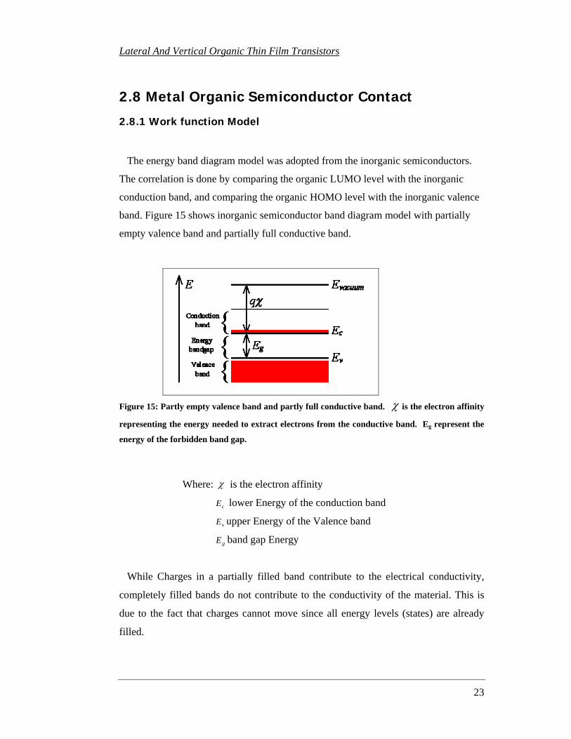
The energy band diagram model was adopted from the inorganic semiconductors.
The correlation is done by comparing the organic LUMO level with the inorganic
conduction band, and comparing the organic HOMO level with the inorganic valence
band. Figure 15 shows inorganic semiconductor band diagram model with partially
empty valence band and partially full conductive band.
Figure 15: Partly empty valence band and partly full conductive band. χ is the electron affinity
representing the energy needed to extract electrons from the conductive band. Eg represent the
energy of the forbidden band gap.
Where: χ is the electron affinity
cE lower Energy of the conduction band
vE upper Energy of the Valence band
gE band gap Energy
While Charges in a partially filled band contribute to the electrical conductivity,
completely filled bands do not contribute to the conductivity of the material. This is
due to the fact that charges cannot move since all energy levels (states) are already
filled.
Lateral And Vertical Organic Thin Film Transistors
24
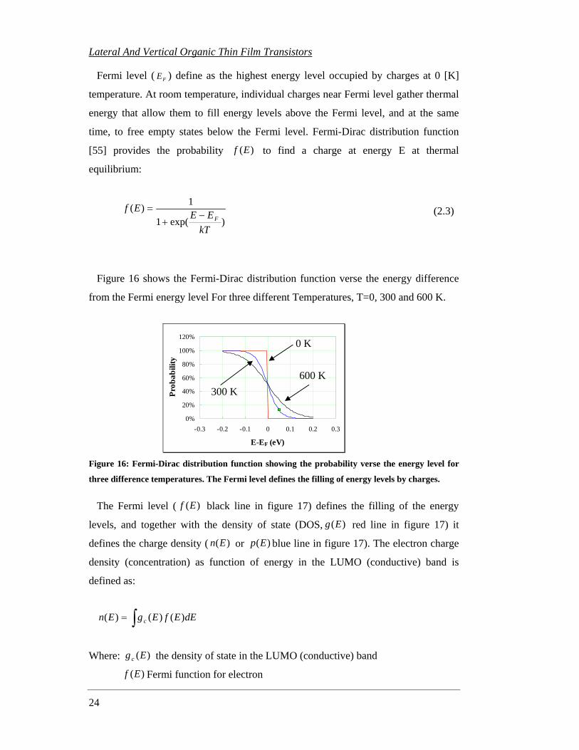
Fermi level ( FE ) define as the highest energy level occupied by charges at 0 [K]
temperature. At room temperature, individual charges near Fermi level gather thermal
energy that allow them to fill energy levels above the Fermi level, and at the same
time, to free empty states below the Fermi level. Fermi-Dirac distribution function
[55] provides the probability )(Ef to find a charge at energy E at thermal
equilibrium:
)exp(1
1)(
kTEE
EfF−
+= (2.3)
Figure 16 shows the Fermi-Dirac distribution function verse the energy difference
from the Fermi energy level For three different Temperatures, T=0, 300 and 600 K.
0%
20%
40%
60%
80%
100%
120%
-0.3 -0.2 -0.1 0 0.1 0.2 0.3
E-EF (eV)
Prob
abili
ty
Figure 16: Fermi-Dirac distribution function showing the probability verse the energy level for
three difference temperatures. The Fermi level defines the filling of energy levels by charges.
The Fermi level ( )(Ef black line in figure 17) defines the filling of the energy
levels, and together with the density of state (DOS, )(Eg red line in figure 17) it
defines the charge density ( )(En or )(Ep blue line in figure 17). The electron charge
density (concentration) as function of energy in the LUMO (conductive) band is
defined as:
∫= dEEfEgEn c )()()(
Where: )(Egc the density of state in the LUMO (conductive) band
)(Ef Fermi function for electron
0 K
600 K 300 K

Lateral And Vertical Organic Thin Film Transistors
25
On the other side, the holes charge density (concentration) as function of energy in
the HOMO (valence) band is defined as:
∫ −= dEEfEgEp v )](1)[()(
Where: )(Egv the density of state in the HOMO (valence) band
)(1 Ef− Fermi function for holes
DOS(E)
f(E)
E
Ef
DOS(E)
f(E)
E
Ef
Figure 17: Fermi-Dirac distribution function (black) and Density of state (red) effecting on the
charge density (blue) [54].
The Fermi level for intrinsic semiconductor ( FiE ) (figure 18) is found at
approximately the mid point between the conduction and valence bands. In this case
the free electrons densities equal to the free holes densities.
HOMO
LUMO
FiE2
sEg
Figure 18: Intrinsic Semiconductor with Fermi level located at the mid band gap between the
LUMO and HOMO levels.

Lateral And Vertical Organic Thin Film Transistors
26
By doping the semiconductor, new energy levels are inserted in the band gap. The
new energy levels are formed below the conduction band for N type doping or above
the valence band for P type doping. This new states push the Fermi level up for N
type dope. On the other hand, the new states push down the Fermi level for P type
dope [figure 19 left, right].
HOMO
LUMO
FiEFdE
HOMO
LUMO
FiEFaE
Figure 19: Doped semiconductor, Left: N-type semiconductor with new states below the LUMO
level pushing the doped Fermi level up, Right: P-type semiconductor with new states above the
HOMO level pushing the doped Fermi level down.
In metals the Fermi level is placed inside one of the bands (figure 20a, b). Most of
highly conducting metals like Copper (Cu), Gold (Au) and Silver (Ag) has one
electron per atom (group 1B at the periodic table) that is free to contribute to the
electrical conductivity [56]. Insulators are materials with high band gap and full
valence gap (figure 20d). The energy needed to extract electrons from the valence
band to the conductive band is much higher compare to semiconductor materials.
Figure 20: Metal, semiconductor and insulator work function; a, b: Fermi level placed inside one
of the bands allows metals charge to move freely inside the band. c: Partially empty valence
band and partially filled conductive band with 1-3[eV] energy band-gap give the specially
properties of semiconductors materials. d: Full valence band with high energy band gap prevents
from charge to move inside the insulator bands or to jump to the conductive band.

Lateral And Vertical Organic Thin Film Transistors
27
When metal and organic semiconductors are brought in unity, a charge adjustment
takes place, in order to get the two materials into common thermal equilibrium. This
equilibrium is reached once the Fermi levels of both materials align. This matching
cause an energy levels banding of the organic semiconductor. Two types of junction
can appear between the metal and the organic semiconductor:
1. Ohmic contact: contact that allow free charge to flow from both materials,
with negligible resistance.
2. Schottky contact: contact that allow unidirectional charge to flow from one
material to the other. This restriction is caused by potential barrier between the
metal and the organic semiconductor.
2.8.2 Ohmic Contact
One way to define an Ohmic contact between metal and organic semiconductor is
that such a contact will not add significant resistance relative to the device bulk
resistance. Other definitions involve equilibrium between the metal and the
semiconductor or that the contact will not significantly change the equilibrium carrier
densities around the contact zone [57]. An Ohmic contact should have negligible
voltage drop across it and linear current voltage relationship. One of the ways to get
this phenomenon in inorganic materials is by heavily doping the semiconductor
surface layer between the bulk semiconductor and the metal contact. This heavy
doping (marks as P++ or N- - for P type or N type respectively) allows free charge
concentrations at the interface, and reduce the potential barrier to a minimum. This
effect allows free charge injection from one material to the other.
The common approach used in organic semiconductor research involve the use of
low work function metal (like Calcium) for negative charge injection to the LUMO
energy level, and high work function metal (like Gold) for positive charge injection to
the HOMO energy level. When the work function of the metal coincide with the
energy of HOMO or LUMO energy levels a thermal equilibrium will allow a net
Lateral And Vertical Organic Thin Film Transistors
28
charge to inject from the metal surface to the organic semiconductor and doped the
interface. In this case an Ohmic contact will exist between the metal and the
semiconductor.
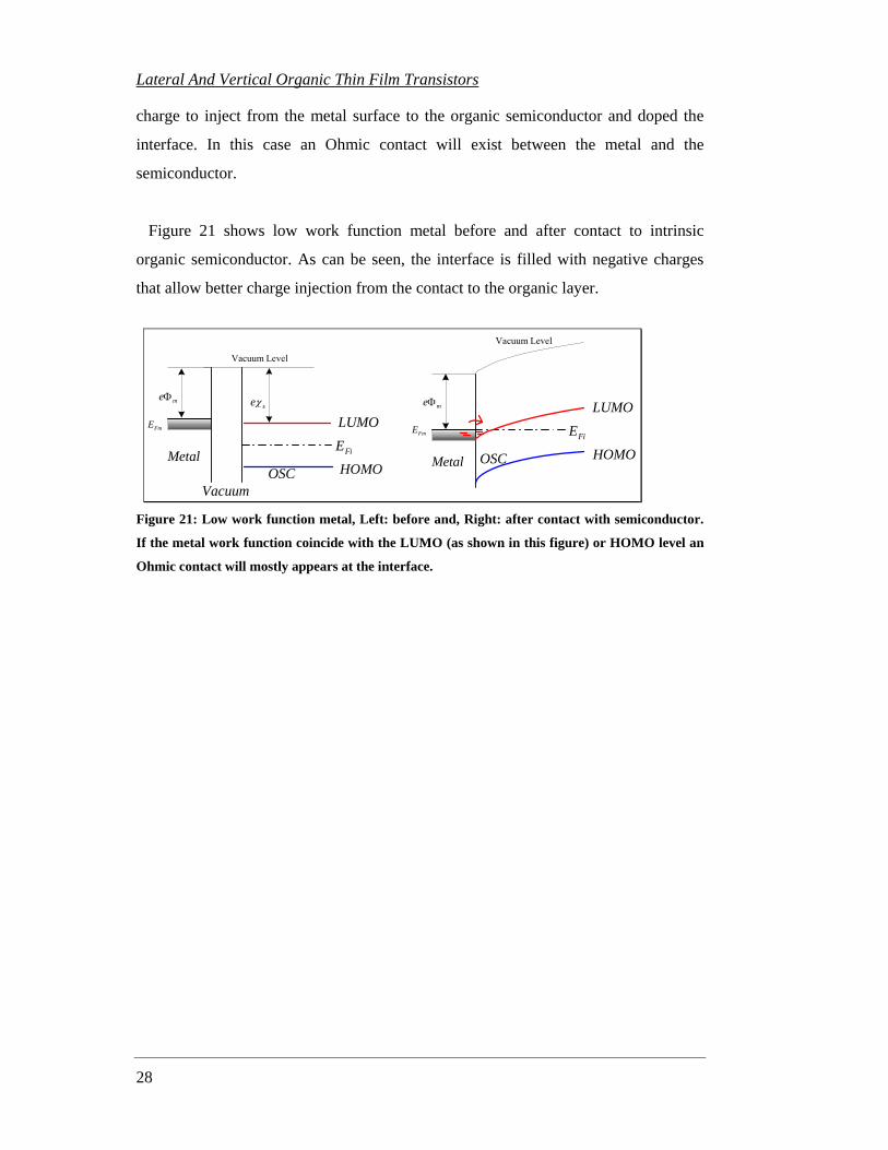
Figure 21 shows low work function metal before and after contact to intrinsic
organic semiconductor. As can be seen, the interface is filled with negative charges
that allow better charge injection from the contact to the organic layer.
Vacuum Level
FmE
meΦseχ
Metal
VacuumOSC
LUMO
HOMOFiE
Vacuum Level
FmE
meΦ
Metal OSC
LUMO
HOMOFiE
Figure 21: Low work function metal, Left: before and, Right: after contact with semiconductor.
If the metal work function coincide with the LUMO (as shown in this figure) or HOMO level an
Ohmic contact will mostly appears at the interface.

Lateral And Vertical Organic Thin Film Transistors
29
2.8.3 Schottky Contact
A Schottky contact appears at metal organic semiconductor interface when the
metal work function is located inside the organic semiconductor band gap. In this case
an energy barrier ( 0Bφ ) is form between the metal contact and the organic
semiconductor (figure 22):
χφ −Φ= mB0 (2.4)
Where: χ Organic Semiconductor electron affinity
mΦ Metal work function
Vacuum Level
FmE
meΦseχ
MetalVacuum
OSC
LUMO
HOMOFiE
0Beφ
Figure 22: When a metal work function is located inside the semiconductor an energy barrier of
size 0Bφ is form between the metal contact and the organic semiconductor, causing a Schottky
contact phenomenon.
This barrier is lowered by the image force induced on the metal surface when
charge (q) is located at distance ( x ) from the metal. The force of attraction between
the charge and the inducted metal charge (-q) define as:
2
2
2
2
16)2(4 xq
xqF
ssi πεεπ
−=
−= (2.5)
Where: sε is the Semiconductor permittivity.

Lateral And Vertical Organic Thin Film Transistors
30
The work needed (Electric potential) to transfer charge from infinity to point x is:
xqdxFxU
s
x
ii πε16)(
2
∫∞
== (2.6)
By applying external field E the electric potential is modified to:
xs
qEx
qxP +=πε16
)(2
(2.7)
Figure 23 shows the image potential energy (black dotted line) as define by formula
2.6 and the energy band diagram effect by the electric field (red line) as define by
formula 2.7.
Vacuum Level
xqEFmE
meΦ seχ
Metal OSCmX
φΔ
iUBneφ
Figure 23: Energy band of metal contact and a vacuum. Image charge line and electric field line
influence on the lowering of the contact barrier. In this figure the Schottky barrier lowering φΔ
and the peak distance from the interface mX can bee seen [57].
The Schottky barrier lowering )( φΔ and the peak distance from the interface )( mX
can be extruded by the condition 0/)( =dxxdP :
EeX
sm πε16= (2.8)
s
eEπε
φ4
=Δ (2.9)

Lateral And Vertical Organic Thin Film Transistors
31
The thermionic emission theory by Bethe [57] is used to describe the charge injects
at Schottky barrier. This theory assumes thermal equilibrium at the interface and
barrier’s height that is much larger compare to thermal energy kT. Two types of
current exist in the interface:
1. Forward current: Electron current density from the semiconductor into the metal
msJ >−
2. reverse current: Electron current density from the metal into the semiconductor
smJ >−
The current density msJ >− is given by the electron concentration which has higher
energy compare to the potential barrier BnFE φ+ :
∫∞
+
>− =BnFE
xms dneJφ
ν (2.10)
Where: xν is the charge velocity in the transport direction.
The electron density nd is defined as the density of state )(EN multiplex with the
distribution function )(EF :
( )
dEkT
EEEcE
hmdEEFENd F
n ⎥⎦
⎤⎢⎣
⎡ −−−== exp*)2(4)()( 3
2/3π (2.11)
Where: m* is the semiconductor effective mass
By determination that the charge energy is defined only by kinetic energy we can
rewrite the following relation:
2*
21 νmEcE =− (2.12)
The net current density in the metal to semiconductor junction can be rewrite as:
smms JJJ >−>− −= (2.13)
Lateral And Vertical Organic Thin Film Transistors
32
This lead to net current density:
]1))[exp(exp(*4 23
2
−−=kTeV
kTeT
hkqmJ aBnφπ
(2.14)
Where: aV is the applied forward voltage
Bnφ is the Schottky barrier height define as: φφφ Δ−= 0BBn (2.15)
By defining 0J (reverse saturation current) as:
)exp(* 20 kT
eTAJ Bnφ−= (2.16)
And A* as the Richardson constants
3
2*4*h
kqmA π= (2.17)
We can rewrite formula 2.14 as:
]1)[exp(0 −=kTeVJJ a (2.18)
Formula 2.18 shows that the forward current will increase exponential as the applied
forward voltage increase.
The reverse saturation current can be rewrite using 2.15 and 2.16 as:
)exp()exp(* 020 kT
ekT
eTAJ B φφ Δ−= (2.19)
Formula 2.19 shows that the reverse saturation current is define by the energy
barrier 0Bφ , but could be increase exponential by reducing the Schottky barrier ( By
increasing φΔ ). Figure 24 shows the energy band diagram of metal and
semiconductor under different reverse bias voltage. By increasing the reverse voltage

Lateral And Vertical Organic Thin Film Transistors
33
from V1 to V3 the Schottky barrier lowering value increase from 1φ to 3φ . This effect
increases the electron injection from the metal into the semiconductor.
Vacuum Level
FmE
meΦ seχ
Metal
1φe3φe
321 VVV <<
OSC1V
2V
3V
Figure 24: Schottky barrier lowering φΔ by applying reverse electric field for different voltage
condition. This figure shows the reduction of the barrier (moving from 1φΔ to 3φΔ ) as the
reverse potential rise (moving from V1 to V3) [57].

Lateral And Vertical Organic Thin Film Transistors
34

Lateral And Vertical Organic Thin Film Transistors
35
33.. LLAATTEERRAALL TTHHIINN FFIILLMM TTRRAANNSSIISSTTOORR
3.1 introductions
This chapter deals with lateral OTFT structure and its basic
operation principles. We briefly describe the state of the art C60
OTFTs thus showing the high quality and the relevance of
understanding the unique features of these devices. This chapter
includes literature survey for published C60 OTFT. The basic TFT
principles are included with definitions for threshold voltage, trap
effect and effective mobility coefficient

Lateral And Vertical Organic Thin Film Transistors
36
3.2 Lateral OTFT structure
Lateral structure is the common architecture found in the semiconductor industry.
This architecture includes horizontal alignment of the source and drain electrodes
while the gate electrode is placed below or above the active semiconductor. Top gate
lateral FET is illustrated in figure 25. This device structure is been used as the basic
element for inorganic CMOS integrate digital circuit.
Figure 25: Top gate lateral FET. This structure is used frequency in CMOS integrated digital
circuit [56].
Figure 26 shows Bottom Gate TFT that is mostly used in amorphous silicon TFT
(ai-Si TFT) and in OTFT.
InsulatorSource Drain
OrganicSemiconductor
GateInsulator
Source Drain
OrganicSemiconductor
Gate
Cd W
InsulatorSource Drain
OrganicSemiconductor
GateInsulator
Source Drain
OrganicSemiconductor
Gate
Cd W
Figure 26: Bottom gate coplanar OTFT. This structure is the common structure for ai-Si TFT
and for OTFT devices. In this structure, the active semiconductor is deposited or spin-coated
over the insulator and source & drain contacts. This process allows inspecting different type
active semiconductor materials while using standard substrate structure.

Lateral And Vertical Organic Thin Film Transistors
37
The TFT architectures consisting of Bottom gate can be divided into coplanar or
staggered structures [22, 58, 59]. The coplanar structure is shown in figure 26. This
device structure includes bottom source and drain contacts, which are evaporated on
top of the insulator layer, before the deposition of the active organic layer. Most of the
C60 transistors in literature are built in coplanar architecture. In this structure the
effective contact area Ca, through which charge is injected into the channel, is
determined by the metal contact thickness (~50 to 100nm) multiplied by the contact
width, Ca=Cd*W (see figure 26). This area is significantly smaller compare to the
contact area found in the staggered structure.
The staggered structure includes top source and drain contacts that are evaporated
over the active organic layer (figure 27).
GateInsulator
OrganicSemiconductor
DrainSource
GateInsulator
OrganicSemiconductor
DrainSource
Figure 27: Bottom gate staggered OTFT. In this structure the drain and source contacts are
evaporated over the active semiconductor layer. This structure was used in this thesis as lateral
OTFT devices.
In the staggered architecture, the contact area is determined by metal contacts area
that overlaps the gate. In this thesis, we used the staggered architecture. In our design
the gate area underlines the channel, source, and drain contacts. This create a
theoretical contact area larger by three orders of magnitude (contact length ~100um
compare to contact thickness ~100nm) compared to the coplanar architecture. This
architecture may be better choice when the contact resistance is the limiting parameter
of the TFT performance [60, 97].

Lateral And Vertical Organic Thin Film Transistors
38
3.3 C60 OTFT – literature survey
First attempt to use Fullerene as active semiconductor in OTFT [61] showed low
mobility in the range of 10-4 [cm2/Vs]. In 1995, work by R.C. Haddon et al. [62]
showed mobility of 0.08 [cm2/Vs] and threshold voltage of 15[V] for C60 evaporated
on N--Si/SiO2 substrate in ultra high vacuum (UHV) system (<10-8 Torr). In addition,
the authors managed to boost the mobility up to 0.3 [cm2/Vs] with negative threshold
voltage of -2.7[V] by using N--Si/SiO2 substrate treatment with tetrakis-
dimethylamino-ethylene (TDAE). TDAE can form 1:1 compound with C60 [63, 64].
The boost in the performance is explained by the formation of C60/TDAE thin layer
complex at the C60/SiO2 interface. The role of this complex was suggested to be in
lowering the barrier to electron injection from the gold electrode to the C60 LUMO
levels. This is supported by the fact that high contact barriers are known to enhance
the effective threshold voltage and reduce the effective mobility [97].
Kobayashi et al. [65] work showed even better mobility of up to 0.5 [cm2/Vs] and
on/off ratio larger then 108. They fabricated and measured C60 OTFT in UHV
(fabrication at <10-9 Torr, measurement at <10-10 Torr). The reported threshold
voltage was still high, VT=17[V] due to Au/ C60 high barrier contacts. In addition,
this group has controlled the C60 film grain size by controlling the substrate
temperature during the evaporation stage. They did not find any correlation between
the grain size and the mobility values.
Exposure of C60 OTFT to ambient air destroyed the field effect current and causes
bulk resistance enlargement by 4 to 5 magnitude order [62]. This suggests that oxygen
penetrate into the film and react with the C60 lattice to create electron traps. These
deep traps are efficient recombination centres for electrons and holes, causing
decreasing in the free carrier density [66]. Konenkamp et. al. [85] shows that the
electronic transport properties are strongly affected when C60 is exposed to oxygen.
Both, hole and electron drift mobilities were found to decrease with oxygen uptake,
while the recombination lifetime increases due to the slower transport.
As the oxygen does not react with the C60 molecule it is possible to extract it under
vacuum. A work that was done by Tapponnier et al. [67] showed that the C60 OTFT

Lateral And Vertical Organic Thin Film Transistors
39
mobility was boosted by one order of magnitude, from 0.08 [cm2/Vs] to 0.5 [cm2/Vs],
by UHV (5*10-7 [mBar]) annealing at temperature of 1200 [C] for two hours. This
indicated that high vacuum annealing could reduce the oxygen traps in the C60 film.
Another group, Kanbara et al. [13], has fabricated “NOT” logic gate from N type
C60 OTFT with mobility of 0.1 [cm2/Vs] and P type Pentacene OTFT with mobility of
0.3 [cm2/Vs]. This group showed that the best C60 OTFT performance was achieved
for 10nm C60 film. Increasing or decreasing the C60 film thickness cause decreased in
the mobility value and increase in the threshold voltage. The best threshold voltage
achieved in this research was 11[V]. In all the above publishing a coplanar shape C60
OTFT devices were used with gold source and drain electrodes. The C60 film was
evaporated on the gold electrode.
Large efforts were invested in synthesis good soluble C60 derivatives. [6,6]-Phenyl
C61 butyric acid methyl ester (PCBM) OTFT has yield mobility of up to 0.023
[cm2/Vs] with 104 on/off ratio [68] (figure 29, right). In 2004, a Japanese AIST group
succeeded in synthesis C60 -fused Pyrrolidine meta-C12 pheryl (C60MC12) with
crystalline micro grain thin film for OTFT. This OTFT has tripled the PCBM mobility
to 0.067 [cm2/Vs] with 105 on/off ratio [69] (figure 28, left).
Figure 28: Two types of synthesis soluble C60 materials for OTFT devices. Left: C60-fused
Pyrrolidine Meta-C12 Pheryl (C60MC12) showing crystalline micro grain gave effective mobility
values of 0.067 [cm2/Vs] [69]. Right: [6,6]-Phenyl C61 Butyric Acid Methyl Ester (PCBM) OTFT
has yield effective mobility of up to 0.023 [cm2/Vs] [68].
Another interesting soluble C60 OTFT was present by Y.Hayashi et al. [70]. This
device includes blend of C60 with P type MEH-PPV conjugated polymer. The device

Lateral And Vertical Organic Thin Film Transistors
40
behaviour, influenced by the MEH-PPV: C60 concentration, changed from P type to N
type properties. Concentration of 1:1 between the MEH-PPVand the C60 gave
ambipolar behaviour with N type and P type mobility in the range of 10-4 [cm2/Vs]
and 10-5 [cm2/Vs], respectively.

Lateral And Vertical Organic Thin Film Transistors
41
3.4 Metal Oxide Semiconductor Capacitor
The core of the TFT is the metal-insulator-semiconductor (MIS) capacitor. One sub-
technology of MIS is the metal-silicon dioxide (SiO2)-semiconductor (MOS)
capacitor, which is used frequently in the industry, and has been used extensively in
this thesis. We used SiO2 insulator due to better leakage performances and better
homogeneity compared to other alternatives.
The OTFT is basically an active organic material (C60 in this Thesis), with source
and drain contacts, which are part of the MIS capacitor as shown in figure 29. By
changing the gate voltage, the MIS capacitor modulates the charge carrier density
near the semiconductor insulator junction. The gate bias induces bending of the
HOMO and LUMO levels relative to the Fermi level near the semiconductor-insulator
interface. In other words, the gate-source voltage attract charge carriers at the
semiconductor-insulator interface, which are induced by the opposite charges carrier
at the gate electrode. The charge carriers inducted at the interface (Channel) reduce
the resistance between the source and the drain electrode and form a conducting
channel. By changing the MIS capacitor voltage polarity or magnitude, we can control
the charge carrier concentration at the interface and by that we control the resistance
between the source and drain electrodes, as shown in figure 29. The region occupied
by charge carriers near the interface and between the source and drain electrodes is
defined as the channel area.
Gate
Ids
Source Drain
Vds
Vgs Gate
Ids
Source Drain
Vds
Vgs Figure 29: Negative charges in the channel induced by positive charge in the gate electrode
reduce the resistance between the source and drain contacts. The external connection includes
Vgs and Vds supply.

Lateral And Vertical Organic Thin Film Transistors
42
3.4.1 Flat band
When metal, insulator and semiconductor materials are joint together to form MIS
capacitor an equilibrium state occurs by Fermi level alignment between the metal
work function and the semiconductor Fermi level (a short between the semiconductor
bulk and the metal contact may be needed to promote this equilibrium). This
equilibrium and the associated charging, causes the HOMO and LUMO levels to bend
near the interface between the semiconductor and the insulator. In addition, it causes a
shift in the vacuum levels of the metal and the semiconductor. Figure 30 shows the
individual MIS materials work function with N type semiconductor before the
contacts.
Metal Insulator Semiconductor
Vacuum Level
SeχLUMO
HOMO
FsEFiE
FmE
meΦ
ieχ
iEg
FeφsEg
Figure 30: Metal, insulator and semiconductor energy levels before physical contact [56].
Figure 31 shows the Fermi level alignment and the energy levels bending of the
semiconductor and the insulator after equilibrium state is achieved.
Metal Insulator Semiconductor
LUMO
HOMOQ−
FmE FsEFiE Q+
Metal Insulator Semiconductor
Figure 31: Fermi level alignment and the energy levels bending of the semiconductor and the
insulator at equilibrium state.

Lateral And Vertical Organic Thin Film Transistors
43
The existence of nonzero potential between the gate material and the semiconductor
cause net charge to appear on both sides of the insulator. The metal-semiconductor
work function difference is equal to:
)2
( Fgs
SMMS qE
φχφφ −+−= (3.01)
Where: Mφ is the metal work function
Sχ is the semiconductor electron affinity
gsE is the semiconductor gap energy
Fφ is the potential difference between the intrinsic Fermi level and the
doped Fermi level. In the case of non-degenerate semiconductors, it is defined by:
i
dtF n
NV ln=φ (3.02)
Where: tV is the thermal voltage ( ekTVt /= , for T=300 K tV =0.00259[V])
dN is the donor doping concentration
in is the intrinsic carrier concentration
The contact potential effect (The different energy levels of the metal and
semiconductor) is not the only one that causes net concentration of charges. A
“Parasitic” charge may exist in the insulator and influence the charge concentration in
the MIS device. This charge consists of the three parts:
1. Interface trap charges exist at the insulator semiconductor interface. It is
caused by defects or dangling covalent bonds at the interface. These
defects trap mobile carriers in the channel, and act as donors or acceptors
points.
2. Insulator trapped charge can exist throughout the insulator bulk. This
charge can be acquired during the insulator fabrication, or through
radiation, photoemission or high-energy injection.
3. Mobile ionic charge. These mobile charges can move through the insulator
bulk by the influences of electric field.

Lateral And Vertical Organic Thin Film Transistors
44
If we will define the “trapped” charge as ssQ and assume it is concentrated close to
the insulator semiconductor interface (as appear in figure 32) then the induced
potential drop across the insulator is:
ins
ssins C
QV −= (3.03)
Where Cins is the Insulator capacitance and is equal to:
ins
insoins t
C εε= (3.04)
Where: oε is the free space permittivity
insε is the insulator relative permittivity
Going back to figure 31, in which the MIS capacitor is in equilibrium without
external potential, we can sum the energy levels as:
00 inssMS V+=− φφ (3.05)
If a gate voltage Vg is applied then the potential drop across the insulator and the
surface potential changes to:
)()( 000 ssinsinssinsg VVVV φφφ −+−=Δ+Δ= (3.06)
By inserting equation 3.05 into 3.06, we get:
mssinsg VV φφ ++= (3.07)
Flat band conditions exist when no charge is present in the semiconductor, and the
Semiconductor energy bands are flat. In this condition, the surface potential equals to
zero, and the charge density on the gate metal should cancel the parasitic charge exist
in the insulator:
0=+ ssm QQ (3.08)
Therefore in flat band condition the gate potential is equal to:

Lateral And Vertical Organic Thin Film Transistors
45
ins
ssmsinsmsg C
QVFBV +=+= φφ)( (3.09)
Metal Insulator SemiconductorMetal Insulator Semiconductor
LUMO
HOMOFmE
FsEFiE
FBVQ+
ssQ−
Figure 32: Flat band conditions after applying external potential VFB needed in order to cancel
any charge in the semiconductor. Left: Flat LUMO & HOMO levels at flat band condition.
Right: Charge distribution appears at flat band condition.
3.4.2 Depletion Mode & Inversion Mode
Surface depletion occurs when the majority charge carriers in the semiconductor
material (electrons in the N type semiconductor) depleted away by the negative gate
voltage. Figure 33 shows the depletion mode.
Metal Insulator Semiconductor
LUMO
HOMOQ−
FmE
FsEFiE
dQ+
Metal Insulator Semiconductor
depV
dX
dX
FeφssQ
Figure 33: Depletion mode appears when the majority charge carriers in the semiconductor
depleted away by the gate voltage. Left: LUMO & HOMO band bending causing depletion of
negative charge from the semiconductor-insulator interface. Right: Charge distribution appears
at depletion condition.
When the Fermi level in the insulator-semiconductor junction is equal to the
intrinsic Fermi level then the depletion layer thickness is equal to:

Lateral And Vertical Organic Thin Film Transistors
46
d
Fsod eN
X φεε2= (3.10)
Where: sε is the semiconductor relative permittivity
Increasing the gate negative voltage also attracts holes (the minority carriers in N
type semiconductor) to the junction, which form the so-called inversion layer. In this
case the Fermi level is crossed by the intrinsic Fermi level, and inversion of the carrier
type appear between the cross point and the insulator-semiconductor junction.
When the holes concentration at the surface and the electron concentration in the
bulk are equal, or in other words, when the HOMO and LUMO levels bend by Feφ2 ,
the maximum depletion layer length is equal to:
d
FsdT eN
X φε4= (3.11)
Metal Insulator Semiconductor
LUMO
HOMOQ−
FmE
FsEFiE
invQ+
Metal Insulator Semiconductor
invV
dX
dX
dQ+Feφ2 ssQ
Figure 34: Inversion mode start to appear when the majority and minority charges concentration
in the semiconductor are equals. Carriers in the Semiconductor depleted away by the gate
voltage. Left: LUMO & HOMO band bending by Feφ2 , Right: Charge distribution at Inversion
mode where inverted charge Qinv carriers added to the depletion charge Qd.
This point known as the threshold inversion point and the applied gate voltage
creating this condition called as the “Threshold Voltage” (VT). Any gate voltage
increscent above this voltage will increase only the inverted charge carrier +Qinv near

Lateral And Vertical Organic Thin Film Transistors
47
the insulator-semiconductor junction and will not affect the depletion layer length
(figure 34).
3.4.3 Accumulation Mode
While inorganic TFT works in inversion mode, organic TFT works in accumulation
mode, where the majority charge carrier are accumulated near the insulator-
semiconductor junction.
For C60 OTFT, negative charge carriers are accumulated in the junction by the
positive gate charge as shown in figure 35.
Metal Insulator Semiconductor
LUMO
HOMOQ−FmE
FsEFiE aQ+
Metal Insulator Semiconductor
VassQ−
Figure 35: Accumulation mode, where the majority charge carrier are accumulated near the
insulator-semiconductor junction. Left: LUMO & HOMO band bending causing accumulation of
negative charge into the semiconductor-insulator interface. Right: Charge distribution appears
at accumulation condition.

Lateral And Vertical Organic Thin Film Transistors
48
3.5 Lateral Metal Oxide Semiconductor TFT
3.5.1 Current Voltage relationship
The linear model describes TFT behavior with small drain source voltage. If we
negligible the drain and source contact effect we could refer to the TFT as linear
device, with channel resistance modulated by the gate source voltage.
In this model we used the following assumptions:
1. The current in the channel is due to drift current, while the diffusion current is
being neglected.
2. There isn’t any current leakage through the insulator layer.
3. We assume that xE
yE xy
∂∂
>>∂
∂. This means we could assume constant electric
field across the channel.
4. Any Insulator charge is being equivalent by charge density at the insulator-
semiconductor interface.
5. The charge carrier mobility in the channel is constant.
The current density across the channel according to Ohm law is:
xx EJ σ= (3.12)
Where σ is the channel conductivity.
For unipolar charge carrier (electrons) the channel conductivity is defined as:
( )yneμσ = (3.13)
Where: ( )yn is the electron concentration in the channel
μ is the electron mobility defined as the charge velocity divided by the
electric field:
Eνμ = (3.14)
The channel charge per unit area is equal to:

Lateral And Vertical Organic Thin Film Transistors
49
∫−=y
ch dyyenQ )( (3.15)
The total channel current is:
∫ ∫∫ ∫ ==y z
x
y z
xx dzdyyenEdydzJI )(μ (3.16)
Integration equation 3.16 and inserting equation 3.15 we get:
xchx WEQI μ−= (3.17)
Where: W is the channel width accepted by integration over z axis.
dxdVE x
x = (3.18)
The channel charge chQ per unit area is assumed to be constant across the channel.
And it is accumulated across the channel after flat band has achieved (the flat band
appears, as define in 3.3.1):
)( )(FBinsmsxgsinsch VVVCQ −−−−= φ (3.19)
Where: Vgs is the gate to source potential
Vx is the potential in the channel at a point x
And the Insulator capacitor per unit area is:
ins
insins t
C εε 0= (3.20)
Where: insεε ,0 are the permittivity of free space and relative insulator permittivity
And tins is the insulator layer thickness
We will define a threshold voltage VT (more in section 3.5.3) as:
)(FBinsmsins
ssmsT V
CQV +=+= φφ (3.21)
Now we can rewrite equation 3.19 as:

Lateral And Vertical Organic Thin Film Transistors
50
)( Txgsinsch VVVCQ −−−= (3.22)
Substituted equation 3.22 in 3.17 gives:
dxdVxWVVxVCI Tgsinsx )( −−= μ (3.23)
Integration 3.23 over the channel length L and the drain source potential Vds gives:
∫∫ −−=d
s
V
V
xTxgsins
L
x WdVVVVCdxI )(0
μ (3.24)
The current Ix is constant and equal to the drain source current Ids:
⎥⎦
⎤⎢⎣
⎡−−==
2)(
2ds
dsTgsinsxdsVVVV
LWCII μ (3.25)
Equation 3.25 can be used as long as | Vds |<| Vgs -VT|. This region is called the
linear region.
However, when drain-source voltage increases above this limit, section of the
channel (near the drain electrode) will move to depletion state, cancelling charge
accumulation at this zone. By increasing the drain-source voltage the channel
depletion zone enlarge. This bottleneck section limits the channel current by
increasing the channel resistance associate with increasing the channel depletion that
is affected by the drain-source voltage. In turn, this dependence causes the channel
current to get into saturation region.
For this case, equation 3.24 integration boundaries are:
∫∫−
−−=Teff VVg
Tgins
L
ds ydVVyVVWCdyyI00
)(])([)( μ (3.26)
Where: Leff is the effective channel length
Vg-VT is the voltage boundaries inside Leff
For long channel transistor (L>>d in lateral transistors) the depletion section is
small compare to channel length (L-Leff <<L). So we can rewrite Leff as L. Integration
of 3.26 gives: (3.27)

Lateral And Vertical Organic Thin Film Transistors
51
⎥⎦
⎤⎢⎣
⎡ −−−=⎥
⎦
⎤⎢⎣
⎡−−=
−
2)(
)(2
)(2
2
0
2T
Tgsins
VVg
TginsdsVVgs
VVWCVVVVWCLIT
μμ
Or: 2)(
2 Tgsinsds VVL
WCI −= μ (3.28)
Equation 3.28 can be used as long as |Vds|>|Vgs-VT|. This region defines as the
“saturation region”. Figure 36 shows the linear (left) and saturation regions (right).
Figure 36: Conductance characteristic for thin film transistor. This conductance figure shows the
linear relations between the drain-source voltage and the channel current for low drain voltage.
For higher drain-source voltage, the channel current enters into saturated region [56].

Lateral And Vertical Organic Thin Film Transistors
52
3.5.2 Equivalent circuit
Staggered shape OTFT can be equivalent to three-region circuit [60, 71] (figure 38):
1. Source contact region – reverse Schottky diode (Ds) with serial resistor (Rs)
2. Channel region – Resistor (Rc) and capacitor (Ci) distributed path
3. Drain contact region – forward Schottky diode (Dd) with serial resistor (Rd)
In addition, parasite capacity (Cp) and insulator leakage resistance (Rl) completing
the equivalent circuit, as appear in figure 37.
Si (G)
SC
Ag (D)Ag (S)
SiO2
L
WSchottkyContact
RchRconDcon
RconDcon
Cch
Si (G)
SC
Ag (D)Ag (S)
SiO2
L
WSchottkyContact
RchRconDcon
RconDcon
Cch
Figure 37: Equivalent circuit for lateral staggered OTFT device. This circuit include non-Ohmic
contacts with serial resistance and channel resistance. In addition the channel capacitance and
contacts parasitic capacitance are shown.
The metal-semiconductor contact energy barrier causes a nonlinear effect that
appears at the contact region. This nonlinear effect can be equivalent to a Schottky
diode with serial contact resistor.
Source
LUMOLevel
C60
Vg
FermiLevel
Drain
FermiLevel
Vs Vd
Rs Rd
DdDsCi, Rc
Source
LUMOLevel
C60
Vg
Drain
FermiLevel
Vs Vd
Rs Rd
DdDsCi, Rc
FermiLevel
Source
LUMOLevel
C60
Vg
FermiLevel
Drain
FermiLevel
Vs Vd
Rs Rd
DdDsCi, Rc
Source
LUMOLevel
C60
Vg
Drain
FermiLevel
Vs Vd
Rs Rd
DdDsCi, Rc
FermiLevel
Figure 38: different view of figure 37 showing the serial components influencing the channel
current of OTFT device. In this figure we have neglect parasitic effects.

Lateral And Vertical Organic Thin Film Transistors
53
The ratio between the contact serial resistor (Rs, Rd), the channel resistor (Rc) and
the diode voltage drop (V(Ds + Dd) gives the Ids- Vds conductance characteristic:
RdLRcRsVVVdsI BDdBDs
ds ++−−
=),(
),(),(μ
ηφηφ (3.29)
Figure 39 shows the conductance characteristic of dihexylquaterthiophene (DH4T)
OTFT [72] with variable channel length (L=2, 0.4, 0.2, 0.1 [um]). By reducing the
channel length the channel resistance reduced, and the nonlinear effect caused by the
contacts become more prominent.
Figure 39: DH4T OTFT [72] with variable channel length. By reducing the channel length the
channel resistance reduced and the non-linear effect caused by the contacts become more
prominent.
Work done by H. Klauk et al. [73] showed that for Pentacene TFT with palladium
contacts, the contact resistance can be about 5 to 10 times greater than the channel
resistance. In this case, the OTFT dynamic performance is limited more by the contact
resistance than the Pentacene carrier mobility. Figure 40 shows the total contact
resistance and channel resistance dependence on the gate-source and drain-source
voltage.

Lateral And Vertical Organic Thin Film Transistors
54
Figure 40: Channel resistance and total resistance for staggered Pentacene TFT as function of
gate source voltage for two different drain-source voltages [73].
The channel resistance decreases with increasing gate-source voltage, due to the
increasing of the gate inducted charge carrier at the channel. Moreover, the contact
resistance decreases, due to the contact-semiconductor barrier lowering, or in other
words, is due to increase of charge carrier density near the contacts that act as contact
doping.
3.5.3 Threshold Voltage
Typically, the threshold voltage is determined as the applied gate voltage needed to
achieve measurable channel current flow. In inversion mode inorganic transistor, the
threshold voltage (in the case of N type semiconductor) defines as the voltage needed
for bending the Fermi level by Fnφ2 :
FnTinsmsT VV φφ 2)( ++= (3.30)
Where Fnφ is the potential difference between EFi to EFn for N type
semiconductor.
)(TinsV is the voltage drop across the insulator at the threshold inversion
point.
Accumulation mode organic transistor does not have exact threshold voltage
determination. The charge accumulation at the channel appears after Flat band

Lateral And Vertical Organic Thin Film Transistors
55
condition achieved. Therefore, few articles define the flat band voltage as the
threshold voltage. The flat band condition depends on the metal-semiconductor work
function difference and on the density of charges trapped in the insulator bulk and
interface (for Ohmic contacts):
ins
ssmsT C
QV +=Ω φ)( (3.31)
As showed in the previous chapter the contact effects are not negligible for OTFT
devices. Because of the intrinsic characteristic of organic semiconductor, most of the
accumulated channel charge carriers are injected from the contacts. In cases where
non ohmic contacts exist, the gate-source voltage need to exceed a critical value to
over come the injected limit caused by the contact energy barrier. And therefore, the
Threshold Voltage includes additional parameter that depends on the contact-
semiconductor energy barrier smsφ and on the organic semiconductor thickness ts:
),()()( ssmsins
ssmsTTT tV
CQinjVVV φφ ++=+Ω= (3.32)
Figure 41 shows the calculated potential, using a 2D device simulation [97],
distribution at the channel. The device was biased in the linear regime (Vgs=-5[V],
Vds=-3 [V]) and the potential and current distributions were calculated. We note that
for the 0.5 [eV] barrier height the potential at the channel underneath the source shifts
towards the gate potential by 0.7 [V]. Since the transistor performance are dictated by
the potential at the channel interface this will also manifest itself as an apparent
increase of the threshold voltage. Matching the source contact work function to the
organic semiconductor bands, and reducing the potential needed for flat band
condition, will cause a reduction in the threshold voltage.

Lateral And Vertical Organic Thin Film Transistors
56
-3.5
-3
-2.5
-2
-1.5
-1
-0.5
0
-2 0 2 4 6 8
VP_T= 0.7V=0.2eV
=0.5eV
Length (μm)
Pote
ntia
l at t
he C
hann
el (V
)
0Bφ
0Bφ
Drain
InsulatorOSC
Source
-3.5
-3
-2.5
-2
-1.5
-1
-0.5
0
-2 0 2 4 6 8
VP_T= 0.7V=0.2eV
=0.5eV
Length (μm)
Pote
ntia
l at t
he C
hann
el (V
)
0Bφ
0Bφ
Drain
InsulatorInsulatorOSC
Source
Figure 41: Calculated potential distribution at the channel interface [97]. The applied bias is
Vgs=-5[V], Vds=-3[V]. The top and bottom lines were calculated for barrier heights of 0.2[eV] and
0.5[eV], respectively.
Schroeder, Majewski and Grell [74] measured the threshold voltage influenced by
the Pentacene semiconductor thickness (figure 42). They showed that the threshold
voltage increase with the Pentacene thickness. This is caused due to electric field
reduction at the contacts-semiconductor interface.
Figure 42: Threshold voltage increase with Pentacene thickness. Transfer characteristic of six
Pentacene OTFT with different Pentacene thickness. The lower threshold voltage was measured
as VT=-0.67[V] for 30[nm] thin Pentacene (plus), while the higher threshold voltage was
measured as VT =-2.69[V] for 930[nm] thin Pentacene (stars) [74].
C60 and Pentacene OTFT are well behaved square law devices. In order to calculate
the VT, we have extract the threshold voltage from the gsd VI ~ transconductance
characteristic when the device was at deep saturation zone (Vds>> Vgs).

Lateral And Vertical Organic Thin Film Transistors
57
3.5.4 Trap Effect
Disorder, defects and impurities located at the OTFT channel and at the insulator-
semiconductor interface are forming trapping states.
Improving deposited conditions, semiconductor purification and insulator substrate
treatment with self-organizing material like octadecyltrichlorosilabe (OTS) leads to
decrease at the traps concentration, and lead to improvement in the OTFT mobility
factor. At poly crystalline organic semiconductor, Like Pentacene and Perylene, traps
mostly appear at the grain boundaries. Insulator treatment with self organizing
material leads to improved surface characteristics and to larger grains size, in which
reduce the grain boundaries traps [75, 76].
Horowitz et al. [77] assumed that when OTFT operating at the threshold voltage,
part of the charges are trapped in the surface traps and only portions of the carriers
participate in the current conduction. When the gate bias is increased, the Fermi level
moves up and more traps are filled. In this case more induced carriers will move
across the channel until a point where all the traps are filled. At this point carrier
charges moves with a constant mobility. Figure 43 shows the traps states located at
the insulator-semiconductor interface filled by the Fermi level rise.
Figure 43: Fermi level rises cause trap’s state located at the insulator-semiconductor interface to
be filled. Left: Without gate bias the Fermi level located in the band gap is far from the
conductive band. In this case the trap’s state below the conductive band is empty of charge.
Right: Rising of the gate bias cause rising in the Fermi level towards the conductive band. This
effect fills the interface traps close to the conductive band [77].

Lateral And Vertical Organic Thin Film Transistors
58
3.5.5 Mobility
The mobility is one of the important parameters that define the TFT quality. The
mobility is defined as the charge velocity divided by the electric field:
Eνμ = (3.33)
Two powerful experiments are used to define the material charge mobility. The
first is time of flight (TOF), where mobile charges are generated by photonic
excitation. The charges are accelerated by external electric field (E). The mobility can
be measured by the time ( tΔ ) it takes the charges to move through a path of distance
(L):
tEL
TOF Δ=μ (3.34)
Other approach is to extract the mobility by current-voltage conductance or
transconductance characteristics of field effect transistor (or TFT in our case) using
equation 3.25 for linear region:
2)(
12,
dsdsTgs
insdslinFE VVVV
WCLI
−−=μ (3.35)
And equation 3.28 for saturation region:
2, )(1
2 TgsinsdssatFE VVWC
LI−
=μ (3.36)
OTFT effective mobility depends on device design materials and geometry and not
only on the Semiconductor intrinsic mobility. This effective mobility depends on the
non-linear contact resistance, traps filling at the insulator-semiconductor interface and
on the electric field existing at the channel.
Many published articles tried to fit equation 3.25 and 3.28 with contact effect [72,
73], trap filling [77, 78] and electric field dependence mobility [60, 79]. Still most of

Lateral And Vertical Organic Thin Film Transistors
59
the publish papers on OTFT characteristics are leaning on equation 3.35 and 3.36 to
calculate the device mobility. In this thesis, we focus on quantity comparison with
other C60 TFT and OTFT publish papers. Therefore, we used equation 3.35 and 3.36
to define the devices mobility. These equations allow us to get variation plot of the
OTFT field effect mobility as a function of the gate and drain voltage obtained from
the trans-conductance graphs.

Lateral And Vertical Organic Thin Film Transistors
60

Lateral And Vertical Organic Thin Film Transistors
61
44.. LLAATTEERRAALL OOTTFFTT PPRROOCCEESSSSIINNGG &&
CCHHAARRAACCTTEERRIIZZAATTIIOONN
4.1 introduction
In this chapter we show the fabrication process of lateral C60 organic TFT. This
process include insulator coated, C60 thermal evaporation, and metal electrodes
evaporation. We characterize the current-voltage response, the threshold
voltage, and the effective mobility value. In the second part, we characterize the
performance of different contact types OTFT. We use a work function model to
explain the performance variation.

Lateral And Vertical Organic Thin Film Transistors
62
4.2 Device processing
4.2.1 Silicon platform
As described in chapter 3, lateral OTFT includes gate electrode, insulating material,
semiconductor organic material, and conducting source & drain electrodes. Due to the
simplicity of the bottom gate staggered shape (figure 28), we used this shape to
fabricate our C60 lateral OTFT. All the fabrication process and measurements are done
in a glove box with a nitrogen atmosphere due to oxygen sensitivity of the C60 organic
material.
The devices are prepared on top of a P-doped silicon substrate with thermally grown
silicon dioxide, which we used as a gate insulator. The thickness of the silicon dioxide
is 50[nm]. This thickness allows us to get low voltage operation, but on the other
hand, this thin oxide layer cause high leakage current and low breakdown voltage
(mostly around Vg~25[V]). These substrates were kept in the glove box until the TFT
evaporating stages.
During the work on this thesis we inspected different types of organic insulators.
For the device that we characterize in chapter 4.2 we used double insulator. The
doped silicon/silicon dioxide substrates were spin coated with PS-b-PMMA
(polystyrene-block-polymethylmethacrylate) insulator. The thickness of the organic
insulator layer was 45 to 50 [nm]. This thickness is adjustable by controlling the
viscosity of the solution and the spin coating rotation speed. We used 1% weight
solution ratio. The rotation speed was 2000 [RPM]. The substrates were rotated for 80
[sec] with 1 [sec] acceleration time. Following the coating process the substrates were
annealed for 12 [hours] at 2500 [C] under dry vacuum condition. This additional
organic insulator double the insulator thickness layer from 50 [nm] to 95-100 [nm].
We refer to the double insulator layer as two serial capacitors with theoretical total
capacity of:
oiox
oioxins CC
CCC+
=*
(4.1)
Where: oxC Silicon dioxide capacity

Lateral And Vertical Organic Thin Film Transistors
63
oiC Organic insulator capacity
The theoretical capacity for SiO2 ( oxε =3.9) devices with 50 [nm] insulator
thickness was calculated as 69 [nF/cm2]. While the theoretical capacity for SiO2/BCP
( oiε =2.5) devices with 100[nm] insulator thicknesses was calculated as 28.3
[nF/cm2]. In parallel, we have inspected the insulator capacity of a SiO2/BCP device
by evaporating metal contact on the insulator layer and inspecting the capacity by
quasi static capacity meter (Agilent 4192A) at frequency of 1[Mhz] and 0.1 [V] AC
swing at 10 [V] DC voltage. The results gave capacity range from 8[nF/cm2] to
17[nF/cm2]. One of the reasons for the incompatibility could arise from defects in the
measurement device contacts. We decided to use the theoretical calculation in order to
get more conservative effective mobility result.
4.2.2 C60 Organic Semiconductor Evaporation
The C60 organic semiconductor was thermally evaporated through a shadow mask
on top of the insulator layer. The doped silicon/silicon dioxide substrates (with or
without the additional polymer insulator layer) were placed in rotate platform with
rectangular mask inside the bell jar evaporator system (EDWARDS, figure 44).
VacuumBell jar
Ceramicboat
for C60
DeviceSubstrate
Motor
Stainless Mask
Mask holder
CryoHead
Tungstenbeddingfor metal
Figure 44: Schematic of the evaporation chamber. The devices are faced down through stainless
mask. The metal or C60 sources are placed at the bottom of the evaporation chamber.

Lateral And Vertical Organic Thin Film Transistors
64
As the vacuum in the bell jar reached 1-6*10-7 [mBar], we started to evaporate the
C60 molecules. The C60 powder, which was placed in ceramic cup below the sample
platform, was heated up to the C60 melting point (~550 [C]). Above this temperature
the C60 molecules start to evaporate from the powder. The temperature was controlled
to result in evaporation rate of 0.05-0.1 [nm/sec], which was monitored with quartz
crystal microbalance. The C60 layer was evaporated to 180-200 [nm] thickness. Figure
45 shows the C60 thin layer on doped silicon/silicon dioxide substrate.
Figure 45: Doped Si/SiO2 wafer (Grey area) after C60 thermal evaporation (Green).
4.2.3 Metal Top Contact Evaporation
An interpenetrating structure mask was used to define the lateral source and drain
contacts. These structure shapes allow us to achieve high channel width (W) to length
(L) ratio. Two masks were used, both with the same channel length of 100 [um]. The
first mask with channel width of 25,000 [um], leading to W/L ratio of 250. The
second mask with channel width of 3,000 [um], leading to W/L ratio of 30.
After replacement of the shadow mask (used to evaporate the C60) with the
interpenetrating structure mask and placing a metal wire (silver, gold or copper) the
platform was evacuated again to 1-6*10-7 [mBar]. After reaching the base pressure the
top metal electrodes were evaporated.

Lateral And Vertical Organic Thin Film Transistors
65
The last stage includes grooving the doped silicon/silicon dioxide substrates at one
corner to expose the silicon bulk. By covering this slit with silver paint we created the
gate contact point. Figure 46 shows the OTFT with the C60 thin layer and the source
& drain & gate (silver paint) contacts.
Figure 46: Two lateral C60 OTFT after top metal contact thermal evaporation (Gray).
No photolithographic procedures were involved during the OTFT fabrication. Most
of the semiconductor organic materials are sensitive to solvent and polymers used
during lithographic process. This fact limit the use of lithographic process only for
bottom contacts organic TFT. On the other hand the uses of mask evaporation
simplify the fabrication process, but limit the lateral channel dimensions to tens of
micrometers

Lateral And Vertical Organic Thin Film Transistors
66
4.3 Measurements and Characterizations
4.3.1 Measurement techniques
Quantifications of the OTFT performance were done by the current-voltage (IV)
characteristics of the conductance and transconductance. The threshold voltage and
the mobility values were estimated from these curves. This measurement allows us
exact measurement of the drain, source and gate current. The measurements were
done with semiconductor parameter analyzer (Agilent 4155B) connected to three
Probes heads (KarlSuss PH100, Figure 47) located inside the glove box with a
nitrogen atmosphere.
60C
Drain Source
Insulator
dV dI
sI
Agilent 4155B
OTFT
gV gI
SiP ++
obeheadPr obeheadPr
Figure 47: Left: OTFT measurements setup. Three probe-heads connected to source, drain and
gate electrodes. The SPA monitor the three channels current while changing two channels, drain
& gate, bias voltage. Right: OTFT in measurement process. The OTFT and the probes heads can
be seen.
All measurements were done in the dark in order to avoid photo-generation of
charges. We used 5 [sec] hold time (the time before the measurement start) and
medium sampling rate during the measurement in order to reduce parasitic charging
effects.
The thickness and roughness of the prepared layers were inspected using scanning
probe micrograph (SPM, Veeco Dimension 3100). The measurements were done in
tapping mode. Tapping mode imaging is implemented by oscillating the cantilever

Lateral And Vertical Organic Thin Film Transistors
67
with nano size tip assembly at or near the cantilever’s resonance frequency using a
piezoelectric crystal (figure 48). The oscillating tip is then moved toward the surface
until it begins to lightly touch, or ”tap” the surface. As the oscillating cantilever
begins to intermittently contact the surface, the cantilever oscillation is necessarily
reduced due to energy loss caused by the tip contacting the surface. The oscillation
amplitude of the tip is measured by the optical detector and input to the SPM
controller electronics.
The feedback loop then adjusts the tip-sample separation to maintain constant
amplitude. The reduction in oscillation amplitude is used to identify and measure
surface features.
Figure 48: Scanning probe micrograph (SPM) at tapping mode. The cantilever’s tip taps at
resonance frequency. The reduction in oscillation amplitude is used to identify and measure
surface features.

Lateral And Vertical Organic Thin Film Transistors
68
4.4 Lateral OTFT I-V Characterization Here we will show result for C60 TFT with SiO2/organic insulator and silver
contacts. The device was fabricated as described in chapter 4.2
4.4.1 Ids – Vds characteristic
First the conductance characteristic was measured. This is done by continuously
varying the source-drain voltage (0[V]<Vds<12[V]) for constant gate source voltage.
This measurement repeat for different gate-source voltage (Vgs=0, 2, 4, 6, 8, 10, 12
[V]). The results appear in figure 49. This figure shows the linear and saturation
regions. The linear slope can be seen for low drain-source voltage, where the TFT is
in the linear region. For higher drain-source voltage the current start to saturate, where
the channel current does not increase with the drain-source voltage.
0
0.05
0.1
0.15
0.2
0.25
0 2 4 6 8 10 12
Vgs=12[V]Vgs=10[V]Vgs=8[V]Vgs=6[V]Vgs=4[V]Vgs=2[V]Vgs=0[V]
Vds [V] Figure 49: Conductance characteristic for C60 OTFT with silicon dioxide/block copolymer
insulator and silver contacts. Drain-source voltage was swap between 0[V] to 12[V] while gate-
source voltage was kept constant. Vgs = 0, 2, 4, 6, 8, 10, 12[V]. (Tr. A)
Additional information that can be extracted from the conductance characteristic is
the contact behaviour. The linear slope from zero drain-source voltage up to

Lateral And Vertical Organic Thin Film Transistors
69
saturation region implies that the contact behaves close enough to an Ohmic contact.
Non-ohmic contacts typically show diode shape character (more on that in 4.5). This
conductance characteristic, shown in figure 49, is typical to inorganic as well as to
high quality organic TFT devices.
By using log-linear conductance graph the “On”/”Off” ratio can be deduced. Figure
50 shows a semi-logarithmic conductance characteristic. By monitoring the gate
current we were able to deduce that most of the “Off” current (green dots where
Vgs=0[V]) was due to bulk conductivity of the C60 film and only very small part of it
was due to gate leakage. As gate-source voltage increased the OTFT switches to the
“On” state where Vgs >VT (here VT < 2[V]). The second conductance line (azure
triangle where Vgs =2[V]) was measured when the OTFT was in the “On” state. We
note that two volt difference in the gate voltage gave one order of magnitude in the
device current (from ~15[nA] to 250[nA]).
10-7
10-6
10-5
10-4
10-3
10-2
10-1
100
0 2 4 6 8 10 12
Vgs=12[V]Vgs=10[V]Vgs=8[V]Vgs=6[V]Vgs=4[V]Vgs=2[V]Vgs=0[V]
Vds [V] Figure 50: Logarithmic linear conductance characteristic for C60 OTFT with silicon dioxide/block
copolymer insulator and silver contacts. (Tr. A)
Increasing the gate-source voltage (up to 12[V]) added another three order
magnitude to the device current (from ~250[nA] to 220[uA]). In general this device
holds “On”/”off” ratio of 104, which is common result compared to other published
OTFT results.

Lateral And Vertical Organic Thin Film Transistors
70
4.4.2 Ids - Vgs characteristic
Secondly the transconductance characteristic was inspected. Here the gate-source
voltage is continuously changed (0[V]< Vgs <18[V]) while the drain-source voltage is
kept constant. This measurement is repeated for different drain-source voltages
(Vds=2, 6, 10, 14, 18 [V]). The results are shown in figure 51.
0
0.1
0.2
0.3
0.4
0 5 10 15
Vds=2[V]Vds=6[V]Vds=10[V]Vds=14[V]Vds=18[V]Fit vt=1.7
Vgs[V]
Figure 51: Transconductance characteristic for C60 OTFT with silicon dioxide/block copolymer
insulator and silver contacts. Gate-source voltage was swap between 0[V] to 15[V] while drain-
source voltage was kept constant. Vds = 2, 6, 10, 14, 18[V]. A theoretical calculation using
equation 3.25 & 3.28 was added (red dots) with threshold voltage 1.7[V] and effective mobility of
1.5[cm2/Vs]. Note that an incompatibility can be seen for Vgs >> Vds the measured currents are
lower then the predicted ones. (Tr. A)
For small gate voltage values the OTFT operates in the saturation region (Where
Vgs-VT< Vds). In this case the channel current depends only on the gate-source voltage
according to equation 3.28, leading to identical current for different drain-source
voltage curve. As gate-source voltage increase, the OTFT operation shifts from the
saturation to the linear region (where Vg-VT>Vds) in which the channel current
depends on the drain-source voltage as well as on the gate-source voltage according to
equation 3.25. At the linear region the different curves are separated due to different

Lateral And Vertical Organic Thin Film Transistors
71
drain-source voltage. A theoretical calculation using equation 3.25 & 3.28 was added
(red dots) with threshold voltage 1.75[V] and effective mobility of 1.5[cm2/Vs] to
figure 51. From this comparison it is clear to see the fit between the theoretical
calculation and the device measurements. While there is good agreement at the
saturation region, a deviation starts to appear at the linear region. The incompatibility
increases as the device operation moves deeper into the linear region (Vgs>>Vds).
A semi-logarithmic graph (Figure 52) can give brighter picture of the different
transconductance regions. After gate-source voltage reaches the threshold limit, the
channel start to build up as indicated by the exponential increase of the device current.
At certain point, the channel extends all the way from the source to the drain (Where
the device moves from saturation region into linear region) and the transfer curves
become linear. At this point incompatibility begins to appear between the theoretical
and measured carves (noticeable for Vds=2, 6[V] where the device enter to deep linear
region).
10-6
10-5
10-4
10-3
10-2
10-1
0 5 10 15
Vds=2[V]Vds=6[V]Vds=10[V]Vds=14[V]Vds=18[V]Fit vt=1.7
Vgs[V]
Figure 52: Logarithmic linear transconductance characteristic for C60 OTFT with silicon
dioxide/block copolymer insulator and silver contacts. Drain-source voltage was kept constant at
Vds =18[V]. A theoretical calculation using equation 3.25 & 3.28 was added (red dots) with
threshold voltage 1.7[V] and effective mobility of 1.5[cm2/Vs]. An incompatibility can be seen for
Vgs >> Vds. (Tr. A)

Lateral And Vertical Organic Thin Film Transistors
72
We need to remember that equation 3.25 & 3.28 deals with ideal transistor
characteristics, which do not refer to the contact resistance, non constant mobility
value and to non constant threshold voltage. If we neglect the last two factors (non
constant mobility value and threshold voltage), we can derive the channel and contact
resistance by inspecting the variation between the theoretical curve and the measured
one.
According to equation 3.29, the device resistance for constant drain-source voltage is:
)()()()(
VgsIdsVdsVgsRVgsRVgsR conchtot =+= (4.2)
Where: Rtot is the transistor total resistance
Rch is the channel resistance and Rcon is the contact resistance
We can calculate the channel and total resistance from the fit current and the
measurements carve that appears in figure 51. In order to get the contacts resistance
we can use the next equation:
)()()(
gsfit
ds
gsds
dsgscon VI
VVI
VVR −= (4.3)
Where: Ifit is the transistor current as defined by equation 3.25 & 3.28
Figure 53 shows the result calculation for resistance value versus gate-source
voltage (0<Vgs<15[V]) and a constant drain-source voltage (Vds =2[V]). The channel
(Rch) and total (Rtot) resistance were calculated directly from theoretical and measured
data, respectively. The contact resistance (Rcon) was calculated using equation 4.3.

Lateral And Vertical Organic Thin Film Transistors
73
103
104
105
106
107
108
2 4 6 8 10 12 14
RchRconRtot
Vgs[V] Figure 53: Contact, channel and total transistor resistance for constant drain-source voltage
Vds=2[V]. While for low gate-source voltage, when the transistor is working in saturation region,
the total resistance is affected only by the channel resistance. At higher gate-source voltage the
contact resistance scale up with the channel resistance. (Tr. A)
For lower gate source voltage(above the threshold voltage), where the transistor is
operating at the saturation region, the total transistor resistance is being influenced
only by the channel resistor due to the high resistance of a depletion zone at the
channel near the drain contact (chapter 3.4). When the transistor working mode is
moving from the saturation region into the linear region the functional form of the
channel resistance is moving from exponential decay into linear decay. The channel
resistance continue to reduce until it become close to the value of the contact
resistance. At this point, the transistor’s total resistance stops to decrease and is being
dominated by both resistors. We could inspect the channel and contacts resistance as
function of drain-source voltage for constant gate-source. Figure 54 shows the
channel, contact and total resistance for Vgs =12[V] and Vds =2, 6, 10, 14, 18[V] that
was extracted using equations 4.2 and 4.3.

Lateral And Vertical Organic Thin Film Transistors
74
0
20
40
60
80
2 4 6 8 10 12 14 16 18
RconRchRtot
Vds[V]
Saturation regionLinear region
Figure 54: Contact, channel and total transistor resistance for constant gate-source voltage
Vgs=12[V]. While for low drain-source voltage, when the transistor is working in linear region,
the total resistance is affected by the contacts and channel resistance. At higher drain-source
voltage, while the contacts resistance is reduce due by barrier lowering the channel resistance
increase. This linear increase halts the saturated current to increase with the rising drain-source
voltage. (Tr. A)
According to the above information, if we assume that the transistor, which works
in deep linear region, is limited by the contact barrier, we could fit Schottky barrier
equation to the conductance characteristic. The channel current and the barrier
lowering can be fitted by equation 3.25 and 2.19 (With fixed Richardson constant) as:
⎥⎦
⎤⎢⎣
⎡−−
Δ−
2)()
)(exp()exp(~)(
20 ch
chTgsconB
dsdsVVVV
kTVe
kTeVI
φφ (4.4)
Where: Schottky barrier lowering φΔ is dependent on the contact potential drop
root conV , and chV is the channel lateral potential drop, leading to:
chconds VVV += (4.5)
We used the following fitting curve:
⎥⎦
⎤⎢⎣
⎡ −−−−=
2)())(()exp(
23
3321mXmXVVmmmY Tgs (4.6)
Where the Schottky barrier lowering )( φΔ can be extracted by:

Lateral And Vertical Organic Thin Film Transistors
75
))/( 32 mmekT=Δφ (4.7)
We have fitted equation 4.6 to one of figure 50 curves (Vgs =12[V] curve, where the
device is working in deep linear region). The fit (black dots) appears in figure 55.
From these curves we can find the barrier lowering for each point as well as the
voltage that drops across the contact. From this fit we could find that the barrier
lowering for Vds =2.5[V] is ][01.0~ eVφΔ and that 35.0~/ dscon VV or that
Vcon~0.87V.
2 10-2
4 10-2
6 10-2
8 10-2
10-1
1 2 3 4 5
Vgs=12[V]
Vds[V]
y = m1*(10.3*m0-((m0) ̂2/2))ErrorValue
3.5134e-050.0027931m1 NA0.00018895Chisq
NA0.96835R2
y = m1*exp(m2*((0.35*m0) ̂0....ErrorValue
7.9733e-060.0028245m1 0.0031030.42023m2
NA1.2211e-07Chisq
NA0.99998R2
Figure 55: Fitting equation 4.4 (black dots) and equation 3.25 (blue dotted line) to part of the
logarithmic linear conductance characteristic taken from figure 50. The red dotted line is the
measured current for Vgs =12[V] and 0.5[V]< Vds <4[V]. In this region the transistor is working
in deep linear zone where the ideal transistor equation 3.25 does not fit well to the measured
data. Including Schottky barrier effect improves the fitting parameters. (Tr. A)
According to figure 52 we learned that when the transistor is working in deep linear
region the classic linear equation does not fit well. We can observe this phenomenon
by fitting equation 3.25, which represent ideal transistor without any contact effects, to
figure 55. This fit (blue dotted line) have high variance R2=0.968. While the black
dotted line represent curve fit according to equation 4.6, which include the Schottky
barrier lowering, with R2=0.999 variance.

Lateral And Vertical Organic Thin Film Transistors
76
4.4.3 Threshold Voltage & Effective Mobility
From the conductance characteristic, it was shown that the threshold voltage lay
between zero to 2[V]. We used the common method for OTFT threshold voltage
extraction. This method includes fitting a linear curve to the square root of the
channel current versus gate voltage in the range where Vds >> Vgs. The linear fit is
presented, according to equation 3.28, in figure 56.
0 100
5 10-4
1 10-3
1.5 10-3
2 10-3
2.5 10-3
1 1.5 2 2.5 3 3.5
Ids^0.5
Vgs[V]
y = -0.0026224 + 0.0014914x R= 0.99966 V
T=1.75[V]
Figure 56: Threshold voltage for C60 OTFT with silicon dioxide/block copolymer insulator and
silver contacts was defined as VT=1.75[V], by fitting linear curve to Ids0.5 Vs. Igs
transconductance graph where Vds =18[V] according to equation 3.28. (Tr. A)
According to figure 56, the threshold voltage is equal to VT=1.75[V]. Extraction of
the threshold voltage allows us to calculate the effective OTFT mobility value* using
equation 3.35 for linear region. Figure 57 shows the OTFT effective mobility value
dependency on the source-drain voltage.
* We define the effective mobility as the value extracted by applying the ideal transistor equation to the
measured currents. This would correspond to the true field effect mobility only in the absence of
contact barriers or any other problem.

Lateral And Vertical Organic Thin Film Transistors
77
0
0.2
0.4
0.6
0.8
1
1.2
1.4
1.6
0 2 4 6 8 10
Vgs=4[V]Vgs=6[V]Vgs=8[V]Vgs=10[V]Vgs=12[V]
Vds[V] Figure 57: Effective mobility factor dependence on drain-source voltage for C60 OTFT with
silicon dioxide/block copolymer insulator and silver contacts. The mobility was calculated using
equation 3.35 for linear region. (Tr. A)
The effective mobility is calculated for each drain-source and gate source
measurement point. One can see that the effective field effect mobility increase with
increasing drain source voltage or with reduction of the gate-source voltage. At both
cases the transistor working region is transferred from deep linear region into
saturation region. The reason for this phenomenon appears due to the reduction of the
contact resistance (barrier) compare to the channel resistance at higher electric fields
or at lower gate-source voltage. This phenomenon was shown in figures 53 and 54. In
order to get a better picture of the mechanisms involved we used equation 3.35 and
3.36 to calculate linear and saturation effective mobility values as a function of the
gate-source voltage. Figures 58 and 59 show the results, respectively.

Lateral And Vertical Organic Thin Film Transistors
78
0
0.4
0.8
1.2
1.6
4 6 8 10 12 14
Vds=18[V]Vds=14[V]Vds=10[V]Vds=6[V]
Vgs[V] Figure 58: Effective mobility value dependence on gate-source voltage. The mobility was
calculated using equation 3.36 for saturation region. (Tr. A)
0
0.4
0.8
1.2
1.6
4 6 8 10 12 14
Vds=10[V]Vds=6[V]Vds=2[V]
Vgs[V] Figure 59: Effective mobility value dependence on gate-source voltage. The mobility was
calculated using equation 3.35 for linear region. (Tr. A)
Figure 58 shows almost constant saturated effective mobility value of 1.5±0.1
[cm2/Vs]. It is clear that the drain-source voltage has no effect in this, saturation

Lateral And Vertical Organic Thin Film Transistors
79
region. While the linear effective mobility for small drain-source voltage (Vds =2[V])
(according to figure 59) seem to reduce from 1.6 [cm2/Vs] to 0.77 [cm2/Vs] as a
function of Vgs. This reduction in the effective mobility value is due to the contact
resistance becoming more significant as the channel resistance goes down. When
dealing with non ideal contacts, which occur often in organic transistor, we should use
the effective mobility parameters extracted from the saturation region in order to get
better realistic information regarding the device performance.
SiO2/BCP insulator and Silver
contacts
VT[V] 1.72
Mobility[cm2/Vs] 1.5+0.1
Table 1: Threshold voltage and saturated effective mobility values for silver contacts SiO2/BCP
insulator transistor. The mix insulator thickness is 100[nm]. (Tr. A)

Lateral And Vertical Organic Thin Film Transistors
80
4.5 Contact Effect on Threshold Voltage & Effective Mobility
4.5.1 Contact Effect (Ag, Cu, Au)
In this part we investigated the influence of the contact type on the OTFT
performance. It is well known that whenever the work function of the metal electrode
does not coincide with the conductive band or in our case with the C60 LUMO level
an injection barrier with non-ohmic electrical behaviour is formed at the metal
semiconductor interface (Chapter 2.8.3). This barrier controls the injection of charges
from the source electrode into the semiconductor channel. In addition it should affect
the device threshold voltage and the device mobility [97]. For this investigation, we
used three different metals as source and drain electrodes: silver, copper and gold,
with work function of 4.3[eV], 4.6[eV] [46, 57] or 4.4-5.4[eV] [111, 112],
respectively, below vacuum level. The metal work function should reach thermal
equilibrium with the C60 semiconductor Fermi level. Because the C60 have intrinsic
characteristics the Fermi level lies close to the mid point at the C60 LUMO & HOMO
band gap. According to that, the C60 Fermi level placed at 4.87 [eV] below vacuum.
When we evaporated the top metals electrodes on the C60 layer, the semiconductor
is slightly doped by the metal until the semiconductor Fermi level matches the metal
work function. This situation appears for the silver and the copper, while it almost
doesn’t appear for the gold evaporation due to similar energy levels between the gold
work function and the C60 Fermi level (Where we define the gold work function as
~4.8[eV]). Figure 60 shows the energy levels of the C60 semiconductor and the work
function values of Silver, Copper, and gold electrodes.

Lateral And Vertical Organic Thin Film Transistors
81
Vacuum Level
Source60C
][57.360 eVC LUMO =
][17.660 eVC HOMO =
FiE
Drain
][3.4 eVe Ag =Φ
A B
A B
60C
Drain Source][6.4 eVe Cu =Φ*][8.4 eVe Au =Φ
gA
uAuC
Figure 60: Left: Work function model of metal contacts and C60 semiconductor before real
contact (*note that the gold work function is known to be very sensitive to its surface properties
and it can move between 4.4 and 5.4[eV] below the vacuum level [111, 112] Right: cross section of
the metal contacts and C60 before real contact.
These figures show the energy barrier between the electrode and the semiconductor.
The barrier between silver and C60 LUMO level is 0.73[eV], the barrier between
copper and C60 LUMO level is 1[eV] and the barrier between gold and C60 LUMO is
0.83-1.83[eV]. According to the work function model we expected to have the
performance drop as we move from silver contact to gold contact.
4.5.2 Ids - Vds characteristic
The OTFTs were fabricated as described in chapter 4.2. Three substrates passed the
same fabricated process up to the source & drain evaporation. At this stage we
evaporated one metal type on each device, leading to three devices having three
different metal electrodes.
We fabricated several batches similar to these devices. The results for the silver and
copper contacts devices repeated themselves, while the gold contacts devices results
were not stable. Few of the gold contacts devices gave strong Schottky effect (like the
device described here), while others gave results that show nearly ohmic effect
behaviour. Explanation appears in chapter 4 summary. The devices were measured in
the same manner as described in chapter 4.3.1. Figure 61 shows the results for
conductance measurements of silver, copper and gold contacts.

Lateral And Vertical Organic Thin Film Transistors
82
0
0.05
0.1
0.15
0.2
0.25
0.3
0 2 4 6 8 10 12
Vgs=12[V]Vgs=10[V]Vgs=8[V]Vgs=6[V]Vgs=4[V]Vgs=2[V]Vgs=0[V]
Vds[V]
Ag contacts
0
0.05
0.1
0.15
0.2
0.25
0.3
0.35
0 2 4 6 8 10 12
Vgs=12[V]Vgs=10[V]Vgs=8[V]Vgs=6[V]Vgs=4[V]Vgs=2[V]Vgs=0[V]
Vds[V]
Cu contacts
0
0.01
0.02
0.03
0.04
0.05
0.06
0 2 4 6 8 10 12
Vgs=12[V]Vgs=10[V]Vgs=8[V]Vgs=6[V]Vgs=4[V]Vgs=2[V]Vgs=0[V]
Vds[V]
Au contacts
Figure 61: Conductance characteristic for C60 OTFT with silicon dioxide and silver (grey, Tr. B),
copper (red, Tr. C) or gold (orange, Tr. D) contacts. Drain-source voltage was swap between 0[V]
to 12[V] while gate-source voltage was kept constant at Vgs = 0, 2, 4, 6, 8, 10, 12[V].

Lateral And Vertical Organic Thin Film Transistors
83
The conductance characteristics of silver and copper contacts show almost ohmic
contacts, while the gold contacts show non-ohmic characteristics. In addition, when
the devices are in saturation region (for example, when Vds >10[V]) the channel
current for the gold contact device is about 15-20% compare to the silver or copper
contacts devices. See figure 62.
0
0.05
0.1
0.15
0.2
0.25
0.3
0.35
0 2 4 6 8 10 12
Ag contactsCu contactsAu contacts
Vds[V] Figure 62: Comparison between silver (grey, Tr. B), copper (red, Tr. C) or gold (orange, Tr. D)
contact devices. Drain-source voltage was swap between 0[V] to 12[V] for constant gate-source
voltage Vgs = 12[V]. The gold contact device current is about 15-20% compare to silver or cupper
devices current.
4.5.3 Threshold Voltage & Effective Mobility
According to the procedure described in chapter 4.4.3 we used fit linear function to
the channel current root versus gate voltage where Vds =18[V]>> Vgs. Due to non
ideal gold contacts pattern line we used fit line from higher voltage (VAu(fit)>5[V])
compare to the other two contacts devices (VAg(fit)>1.5[V] and VCu(fit)>2.5[V]).
The results are shown in figure 63.

Lateral And Vertical Organic Thin Film Transistors
84
The silver contacts threshold voltage equal to VT=1.06[V], the copper contacts
threshold voltage equal to VT=1.68[V] and the gold contacts threshold voltage is
VT=2.48[V]. All the VT fit carve were done with variance higher than R2=0.996.
0
0.001
0.002
0.003
0.004
0.005
0.006
0.007
0 2 4 6 8 10
Ag(I^0.5) Cu(I^0.5) Au(I^0.5)
Vgs[V]
y = -0.0022163 + 0.0020861x R= 0.99863
y = -0.0033697 + 0.0019963x R= 0.99947
y = -0.0018893 + 0.00076135x R= 0.99983
Ag_fitCu_fitAu_fit
y = -0.0022163 + 0.0020861x R= 0.99863
y = -0.0033697 + 0.0019963x R= 0.99947
y = -0.0018893 + 0.00076135x R= 0.99983
Figure 63: Threshold voltage for C60 OTFT with silicon dioxide insulator and silver (grey, Tr. B),
copper (red, Tr. C) or gold (orange, Tr. D) contacts was defined as VT=1.06[V], VT=1.68[V],
VT=2.48[V] respectively. The linear carve fit was done to Ids0.5 Vs. Igs transconductance graph
where Vds=18[V] according to equation 3.28
From the definition of the threshold voltage we could calculate the OTFT effective
mobility versus the contact type. The effective mobility calculation was done in
similar manner as described in chapter 4.4.3. Figure 64 shows the saturation regions
OTFT effective mobility.

Lateral And Vertical Organic Thin Film Transistors
85
0
0.2
0.4
0.6
0.8
6 8 10 12 14
Ag_Vds=6[V]
Ag_Vds=10[V]
Ag_Vds=14[V]
Ag_Vds=16[V]
Cu_Vds=6[V]
Cu_Vds=10[V]
Cu_Vds=14[V]
Cu_Vds=18[V]
Au_Vds=6[V]
Au_Vds=10[V]
Au_Vds=14[V]
Au_Vds=18[V]
Vgs[V]
18[V]
Figure 64: Effective mobility factor dependence on gate-source voltage for silver (grey, Tr. B),
copper (red, Tr. C) or gold (orange Tr. D) contacts. The mobility was calculated using equation
3.36 for saturation region. Drain source voltage kept constant for Vds =2, 6, 10, 14, 18[V]
The effective mobility figures for each device show similarity to the mobility
figures describe in chapter 4.4.3. A small reduction in the effective mobility can be
seen for silver and copper contact devices. As expected, the gold contact effective
mobility is significantly lower compared to silver or copper contact devices. This can
be explained by the higher barrier existing at the interface between the gold source
electrode and the C60 semiconductor. On the other hand, according to the work
function model we expected that the silver contact device would show better effective
mobility compare to the copper device. Summary of the threshold voltage and
efficiency mobilities values are shown in the next table.
Silver contacts Copper contacts Gold contacts
VT[V] 1.06 1.68 2.48
Mobility[cm2/Vs] 0.37+0.08 0.4+0.07 0.06+0.013 Table 2: Threshold voltage and saturated effective mobility values for silver (Tr. B), copper (Tr.
C) and gold (Tr. D) contacts SiO2 insulator transistor. The insulator thickness is 50[nm]

Lateral And Vertical Organic Thin Film Transistors
86
4.6 scanning probe micrograph (SEM) images
One of the reasons for the superior performance of the block copolymer insulated
device compare with the SiO2 insulated device could be related to the C60 film
morphology growth in the channel during the evaporation process. C60 crystal grains
increases due to better order influence by insulator layer means better order OTFT
channel morphology, and could enhanced the device performance. For Pentacene
OTFT there is direct correlation between the semiconductor grains size to the device
performance [21, 24, 73, 77, 80b], while in C60 OTFT Kobayashi et al [65] tried to
inspect the coronation between C60 grain size (by controlling the substrate temperature
during the evaporation stage) and the device performance. No correlation was found.
To check the different C60 film morphology evaporated on block copolymer or SiO2
we used scanning probe micrograph working in tapping mode. Figures 65 and 66
show the scan thickness and phase images results for Si/SiO2/block-copolymer and
Si/SiO2 substrate evaporated with ~10[nm] C60 thin films, respectively. The scan size
was 1[um]. Both devices gave more or less the same film morphology, with average
grain size of 100[nm]. There is no evidence for larger or rigidity C60 grains size for the
block copolymer model.

Lateral And Vertical Organic Thin Film Transistors
87
Figure 65: SPM scan for Si/SiO2/block-copolymer/ C60 (~10[nm]). Left: Roughness image, Right:
Phase image.
Figure 66: SPM scan for Si/SiO2/ C60 (~10[nm]). No variation in grain size or rigidity compare
with figure 65.

Lateral And Vertical Organic Thin Film Transistors
88
4.7 Summary
The C60 lateral OTFT presented in this chapter showed good similarity to the ideal
transistor theoretical formulas using Schottky effect barrier correction. We showed
that for the saturation region, where the contact resistance are much lower compare to
the channel resistance, we could use the ideal transistor theoretical formulas.
However, as the transistor operating conditions are changed towards the linear region,
where the contacts resistance aren’t negligible any more, we need to take in to
account the effect of the contacts. This is essential for non ohmic contacts.
Threshold voltage and effective mobilities values were extracted using only the
ideal transistor formulas. For our best knowledge the block copolymer insulator C60
OTFT results (shown in part 4.4.3) are the best performance C60 OTFT ever
published. The effective mobility is three times larger compare to the best publish C60
OTFT [65, 67]. These effective mobility and threshold voltage put the N type C60
OTFT in the same performance level as amorphous silicon TFT or Pentacene OTFT.
Block copolymer insulator C60 OTFT effective mobility was three times larger
compare to silicon dioxide insulator. The device mobility increase can be explained
by reducing trap states or/and better ordering of the C60 molecules in the
semiconductor channel. In part 4.6 we tried to show relations between the superior
performance devices and the C60 thin layer grains sizes. Larger grains size will cause
better order in each grain domains and reduce the charge carrier scattering at the
grains boundaries between the contacts. According to SPM scan there wasn’t any
morphology difference between the better performance block copolymer insulated
device compare with the SiO2 insulated device. It could be that the differences are
confined to the channel surface and require farther investigations.
Silver and copper contacts C60 OTFT gave better performance compared to gold
contacts devices. Most of the published C60 OTFT devices used gold contacts, which
lower the device performance due to high source contact barrier. By suitable choice of
metal which forms a lower Schottky energy barrier, like silver or copper, the
transistor performance was improved. We tried to show direct relationship between

Lateral And Vertical Organic Thin Film Transistors
89
the device contact barrier and the device mobility and threshold voltage according to
the work function model. This relationship wasn’t clear enough. We have fabricated
several batches with silver, copper and gold contacts. The results for the silver or
copper contacts devices were reproducible, while the gold contacts devices results
vary from strong Schottky parameters, like the transistor presents here, up to almost
ohmic parameters. In addition, according to the work function model, we expected to
get better device result using silver contacts compared to copper contacts. But both
contacts devices performance were similar. The reason for that can be attributed to
various factors, including the built in stress in the semiconductor due to the metal
evaporation, causing damage to the organic film ordering and increasing the interface
traps states, other influence could rise due to interpenetration of the metal inside the
active layer, influencing the interface dipole parameters.
The effective devices mobility increases with increasing drain-source voltage. This
phenomenon can be explained by source contact barrier reduction, due to stronger
source drain electric field. On the other hand, when the device is working in linear
region the effective mobility decreases as the gate-source voltage increases. This
happened due to the increased influence of the contact on the total resistance. We
showed that as we entered deeper into the linear region the channel resistance reduce
to minimum, in this region the contact resistance become more dominant and the total
device conductivity do not increase as excepted, leading to deviation from the ideal
curve as can be seen in figure 51.
Tr.
Ins.
Type
Contact
Type
Tox
[nm]
Vt
[V]
Mobility
[cm2/Vs]
A SiO2/BCP Ag 100 1.72 1.5+-0.1
B SiO2 Ag 50 1.06 0.37+-0.08
C SiO2 Cu 50 1.68 0.4+-0.07
D SiO2 Au 50 2.48 0.06+-0.013 Table 3: Summary of lateral transistors shown in this thesis.

Lateral And Vertical Organic Thin Film Transistors
90

Lateral And Vertical Organic Thin Film Transistors
91
55.. NNOOVVEELL VVEERRTTIICCAALL OORRGGAANNIICC
TTHHIINN FFIILLMM TTRRAANNSSIISSTTOORR
5.1 introduction
This chapter discusses the benefit of vertical OTFT compared to
lateral OTFT and relevant published contributions by other groups
are presented. The basic theory for the operation of our new
structure, PS-OVTFT, and background on the technology that utilize
block co-polymer is discussed.

Lateral And Vertical Organic Thin Film Transistors
92
5.2 Vertical OTFT
5.2.1 Benefit of Vertical TFT
The organic TFT performances are still poor compared to inorganic devices. Most
of the efforts are still focused on the traditional lateral TFT structure. Among the
efforts we can find approaches that try to reduce the contacts resistance or the
trapping states of the insulator-semiconductor interface. Other common directions
include efforts to increase the dielectric constant of the gate dielectrics or reduce the
channel length [80-84].
In the margins of the OTFT research few academic groups are trying different
approaches by using vertical shape OTFT, in which the channel length is defined by
the thickness of the organic layer and not by the high resolution photo lithography
process needed for lateral OTFT. Apart from the fabrication price reduction, these
devices should have enhanced DC performance and better switching speed. In the
following pages we will describe five reports of attempts to boost the OTFT
performance by utilizing a vertical structure.
The common feature of all the reported device structures is that the source and drain
are vertically stacked and are separated by the thickness of the semi-conducting or the
insulating organic layer. The differences are in the location of the semiconductor layer
and of the gate electrode.
5.2.2 Vertical OTFT in literature
Stutzmann et. al. produced self-aligned Vertical channel polymer FET [30] which is
similar to the V-groove FET [57]. The unique fabrication procedure in that paper is
the use of solid state embossing to produce the device. Embossing is non lithographic
patterning technique capable of imprinting nano scale patterns into polymer thin layer.
The process was done with micro cutting tool having sharp wedges that could
penetrate into a multilayer of metals contacts and semiconductor film.

Lateral And Vertical Organic Thin Film Transistors
93
First, they fabricated a tri-layer structure consisting of a polymer insulator layer
bounded between two electrode layers (figure 67a). These layers were evaporated or
spin coated on a PET substrate. Secondly, they pressed the emboss mold Forming a V
shape inside the tri layer structure (figure 67b). Finally, they coated the V shape
channel with polymer semiconductor, polymer gate insulator and gate electrode
(figure 67c). The channel length was defined by the insulator layer thickness (between
700 to 1200 [nm]).
Figure 67: Fabrication steps for the self-aligned vertical channel polymer FET [30] design by
Stutzmann et. al: a) The substrate with the source and drain electrode before the embossment
process; b)The substrate after the embossment; C) The device include the source and drain
contacts, semiconductor, insulator and gate electrode.
F8T2 polymer semiconductor was used as the active layer. The mobility extract for
this device gave 2-3*10-3 [cm2/Vs], which is similar to mobility extract from lateral
F8T2 TFT. On the other hand, the conductance characteristics (figure 68) include
linear relationship between the drain-source voltages to the channel current, and lack
the typical lateral structure saturation zone.
a)
b)
c)

Lateral And Vertical Organic Thin Film Transistors
94
Figure 68: Conductance characteristics for F8T2 self-aligned vertical channel polymer FET [30]
L=900[nm], W~500[um]; inset: F8T2 chemical structure.
The Schottky barrier between the source contact and the F8T2 HOMO Level
(F8T2HOMO~5.5[ev] compare to Auwork function~4.8[eV]) limited the injected current and
the device performance. By replacing the active polymer to P3HT
(P3HTHOMO~4.9[ev]) the contact resistance was reduce to minimum and the mobility
factor was enhancement to 1*10-2 [cm2/Vs]. Figure 69 shows the P3HT device
conductance characteristics. The relatively high off currents (when Vg=0) are
attributed by the authors to unintentional P3HT doping.
Figure 69: Conductance characteristics for P3HT self-aligned vertical channel polymer FET [30]
L=900[nm], W~500[um]; Inset: P3HT chemical structure.
R. Parashkov et. al. organic vertical channel transistor structure [86] is similar to
Stutzmann et. al device. This group used excimer laser in order to define the source
and drain contact pattern (figure 70).

Lateral And Vertical Organic Thin Film Transistors
95
Figure 70: Parashkov Vertical-channel [86] fabrication process: (a) Drain electrode deposition;
(b) insulating layer deposition; (c) source electrode deposition; (d) formation of the vertical
channel by excimer laser ablation through Cu mask; (e) schematic of the vertical channel; W-
channel width, L-channel length.
Channel length was estimated to be 2.3 [um], dictated by the thickness of the PVP
insulator layer. This thickness was necessary because of the high average roughness
of the gold contacts and the need to get an insulated layer free of pinholes. After the
definition of the source & drain contacts a Pentacene active organic layer was
evaporated following by gate insulator layer coated and casting of PEDOT/PSS stripe
as gate electrode (not seen in figure 70). Figure 71 shows the vertical OTFT
characteristics for PEDOT/PSS contacts (a, b) and for gold contacts (c, d). The
mobility was estimated to be 3.42*10-3 [cm2/Vs] and 1*10-3[cm2/Vs] for PEDOT/PSS
and gold contacts, respectively.
Figure 71: Parashkov Vertical-channel Conductance and transconductance characteristics [86]
for: a-b) Conductive polymer source-drain electrodes; c-d) Gold source-drain electrodes.

Lateral And Vertical Organic Thin Film Transistors
96
The third structure, K. Kudo group’s static induction transistor (SIT) [31-32, 87] is
based on an inorganic thyristor structure [88] proposed in 1975. The roots for this
structure go even further to 1904 and are based on the electric vacuum tube principle
patent by John Ambrose Fleming. The SIT is based on combination of organic diode
with Schottky gate electrode. Kudo et. al. used copper phthalocyanine (CuPc) film as
an active layer. CuPc make an ohmic contact with the Au source & drain electrodes,
and form a Schottky barrier contact with the Al gate electrode. Figure 72 shows the
SIT structure, CuPc chemical structure and the device top & side view. SIT side
profile expose (fig 72) the gate electrode striped shape. Much of Kudo group’s efforts
are invested in pattering this shape. Still this structure cause fabrication difficulty and
limit the current modulation.
Figure 72: Kudo et. al. Static induction transistor (SIT) structure [87]: a) SIT structure; b) CuPc
chemical structure; c) SIT upper and side view
In this device the injected carriers from the source flow toward the drain region
through the potential barrier near the gate stripes electrodes. The carriers flow is
controlled by the potential barrier height depending on the gate voltage. Figure 73
shows the SIT potential diagram. Increasing the gate electrode potential creates a
barrier and reduces the charge carrier flow between the source and drain electrodes.

Lateral And Vertical Organic Thin Film Transistors
97
Figure 73: SIT energy band diagram [32], with positive gate voltage.
As seen before, the conductance characteristic (figure 74) shows diode
characteristics controlled by the gate field effect. The channel current reduces as the
gate potential increase, and no current saturation appears. The mobility extracted from
this device [87] is still low (4*10-6 [cm2/Vs]). The author claims for low leakage
current smaller then 10-8 [A] when Vg<0.8 [V]. At this dynamic range
(0[V]<Vg<1[V]) the On/Off ratio is lower than 10.
Figure 74: SIT conductance characteristics [32] for different gate voltage.
Nakayama et. al. charge injection controlled transistor (CICT) [89, 90] has similar
structure to SIT structure but includes flat gate electrode. According to Nakayama the
CICT mechanism is based on hot electrons, where the emitter current flows through
the base electrode to the collector electrode, and is modulated by base voltage. This
structure is similar to the metal base transistor (MBT) used in in-organic electronics.
Figure 75 shows the CICT structure and the measurement circuit. C60 and N’-

Lateral And Vertical Organic Thin Film Transistors
98
b)
dimethyl-3,4,9,10-perylene tetracarboxylic diimide (Me-PTC) organic
semiconductors gave the best performance for this structure.
Figure 75: Nakayama et. al. charge injection controlled transistor (CICT) [90] structure include
the measurements circuits
Increase of the base potential will cause the base and collector currents to rise.
Figure 76 shows the collector current and the current amplification factor (hFE), define
as the ratio between the output (collector) current to the input (base) current.
Figure 76: CICT: a) Collector current Vs. Collector Voltage, b) Current amplification factor
(hFE), define as the ratio between the output (collector) current to the input (base) current under
different base voltage [90].
The last structure is, Liping Ma et. al. gate-source-drain vertical organic field effect
transistor (VOFET) [33]. Like SIT this structure includes horizontal active layer and
gate electrode. But here the gate electrode is placed below the source electrode. The
authors define this structure as active cell on top of a capacitor cell. Figure 77 shows
the schematic diagram of the VOFET.

Lateral And Vertical Organic Thin Film Transistors
99
a)
Figure 77: Ma et. al. gate-source-drain vertical organic field effect transistor (VOFET) [33]: left:
VOFET structure and schematics of the common source electrode roughness; right: Atomic force
microscope image of the source electrode surface
Ma et. al. state two important conditions needed for operation of the VOFET device:
1. Thin and rough common source electrode.
2. High capacitance for the bottom capacitor cell.
The common source electrode is formed from evaporating of 20[nm] copper and
10[nm] aluminium. Figure 77 right shows AFM image of the common source
electrode, which emphasize the roughness of this layer. The model described in the
paper defines that electric field produced by the bottom charged capacitor cell is not
totally shielded at the source/organic interface due to the rough interface and net
charges at the surface. This electric field inducted negative charge on the top surface
of the source electrode, as well as, positive charge in the organic layer, near the
source/organic interface result in lowering the barrier height (figure 78) between the
source and the organic layer.
Figure 78: VOFET band diagram as describe by Ma et. al [33]: a) without gate voltage; b)With
positive gate voltage

Lateral And Vertical Organic Thin Film Transistors
100
Ma et. al. device impressive performance include 10[mA] channel current at Vds
=4[V] and Vgs =5[V] with On/Off ratio close to 4*106. Figure 79 shows the
conductance characteristics for this device.
Figure 79: VOFET [33] conductance characteristics for difference gate-source voltage
The channel current is sufficient to drive an organic light-emitting diode (OLED).
Figure 80 shows a 1000 cd/m2 bright OLED driven by this VOFET.
Figure 80: OLED driven by the VOFET device [33]. The OLED and the VOFET circuit appear
in the inset. When the gate-source voltage is 0[V] then most of the 8[V] fall on the high resistance
active cell. When the gate-source voltage is 4[V] the active cell resistance drops to 3[V], allowing
light emission from the OLED cell.

Lateral And Vertical Organic Thin Film Transistors
101
5.3 Patterned Source Vertical Organic Thin Film
Transistor
5.3.1 Block Co Polymers (BCP)
The ability to obtain two or three dimensions nano scale self-assembly
patterns makes block copolymer a candidate to various applications. The block
copolymer provides access to scales that are not available to traditional lithographic
techniques, and can be considered as nano lithographic masks. These patterns have
inspired a variety of new applications as nano filters for fuel cells, structured blocks
for memory stack capacitors [91-93], solid electrolyte batteries, membrane for drug
delivery, and structured blocks for optoelectronic devices.
An interesting use of the block copolymer concept is to better mix N type and
P type organics semiconductor materials. These boundaries boost the separation
process of electrons and holes in photovoltaic cells. On the contrary, it could boost the
efficiency of the recombination sites in a light emitting diode. In one of the interesting
works done in the science of integration between block copolymer and organic
semiconductor, Hadziioannou et al. demonstrated [94-96] the formation of
photovoltaic cells made from electron donating (PPV) and electron accepting (C60)
block copolymers. The PPV-b-P(S-stat-C60MS) diblock copolymer synthesis by
Hadziioannou group for the photovoltaic cell appears in figure 81.
Figure 81: Chemical structure for donor-acceptor diblolck copolymer PPV-b-P(S-stat- C60MS)
synthesis by Hadziioannou group for the photovoltaic cell [94].
A block copolymer consists of two or more polymeric chains (blocks), which
are covalently attached to each other. When the constituent polymers are

Lateral And Vertical Organic Thin Film Transistors
102
incompatible, phase separation will take place, leading to segregation of
the different blocks to distinct domains (phases) [98]. The covalent bond
between the blocks prevents phase separation on a macroscopic scale, thus
the phase separation process leads to materials that feature nano-scale periodic
morphologies. Moreover, the tendency of phase-separated systems to minimize
the interfacial energy leads in block copolymers to the formation of
lamellae, cylinders, and spheres depending on the relative volumes ( if ) of the
blocks [99, 100]. When the volume fraction of block A ( Af ) is small, the resulting
structure is of spheres made of block A surrounded by block B material. As the
volume ratio of block A ( Af ) increase towards ratio of 0.5, cylinders in a hexagonal
lattice (figure 82: C cubic), bicontinuous double gyroid (figure 82: G cubic), and
finally lamellae (figure 82: L cubic) structures are formed respectively. When the
ratio ( Af ) is above 0.5 a mirror structure appears, in these structures block A become
the dominant material (figure 82: G’, C’, S’ cubic).
Figure 82:Structural 3D pattern of block copolymer [100]: a) Theoretical phase diagram
predicted by self-consistent meanfield theory; b) Experimentally phase diagram; c) Block
copolymer geometries as a function of relative lengths of the two blocks.
The patterns assumed by the block copolymers are influenced by the boundary
conditions as well the films interface or thickness. Work done by R. Magerle et
al.[102] shows the effect of film thickness on the copolymer structure. Figures 83 a, b
are SPM images, taken in phase mode, of a thin poly(styrene-b-butadiene-b-styrene)
tri-block copolymer film as a function of its thickness. Figure 83c shows the

Lateral And Vertical Organic Thin Film Transistors
103
schematic profile of a & b images, and figure 83d gives a simulation image of the
block copolymer structure.
Figure 83: Block copolymer boundary conditions influence by film thickness [102]; a-b) Phase
SPM images of a thin poly (styrene-b-butadiene-b-styrene) triblock copolymer which
reconstructs as a function of film thickness.; c) Schematic height profile of the phase images; d)
Simulation of the block copolymer.

Lateral And Vertical Organic Thin Film Transistors
104
5.3.2 PS-VOTFT Structure
The structure we propose to use is patterned source vertical OTFT (PS-VOTFT)
which looks similar to the one used in Liping Ma VOFET device [33]. The main
obstacle in constructing this structure is the possible shielding of semiconductor film
from the gate voltage by the source electrode. The solution that we chose for this
problem was the use of a grid like source electrode, which will allow the gate field
flux pass through the grid at the regions which are not covered by metal. As we will
see below, this unique choice of electrode makes the device operation very different
to that reported by Ma et. al. [33].
In our structure the field flux should attract charge carrier from the source metal to
the exposed regions at the semiconductor-insulator interface in a manner very similar
to that of filling the channel in a lateral OFET. Since the choice of metal is such that
there is barrier to charge injection into the semiconductor, such injection will be
accompanied by bending of the semiconductor HOMO & LUMO levels. The current
injection from the source metal thus is being controlled by the level bending, which is
adjusted by the gate electrode potential.
Figure 84: Schematics of the proposed novel patterned source vertical OTFT (PS-VOTFT)
including the Gate electrode, Insulator, source grid, semiconductor and drain electrode.
When dealing with film layers measured at the tens of nanometer scale, we need to
understand that the grid segment should be shorter then the semiconductor layer
thickness. For our best knowledge, block copolymer is the only simple technique that
enables nano scale two dimension patterns. The main problem was to find way to

Lateral And Vertical Organic Thin Film Transistors
105
transfer the block copolymer pattern into conductive metal electrode that will be used
as the source electrode. An article published at Nature magazine [103] by Lopes &
Jaeger unroll us the path for patterning nano scale conductive metal surface using
block copolymer film.
5.3.3 Patterned Source electrode
5.3.3.1 BCP Pattern
The idea behind Pattern Source contact used in our PS-VOTFT device was to use
bottom up method in which the block copolymer layer guide a metal source layer.
This technique is based on work done by W. A. Lopes and H. M. Jaeger [103, 104].
The technique is based on the different wetting properties of the block copolymer
materials, and the use of these properties to guide diffusing metal atoms to aggregate
selectively. This process produce highly organized metal nanostructure.
We used asymmetric polystyrene-block-polymethylmethacrylate (PS-b-PMMA)
that formed parallel cylindrical domains PMMA blocks surrounded by PS blocks with
repeat spacing of 40-50 [nm]. Mansky et al. showed [105-108] that a PS–PMMA
block copolymer could be attached to the substrate surface and would induce
perpendicularly lamellar-forming structures. In this case, smooth films are observed
only when the original, spun-cast film thickness matches a natural thickness of NL,
where N is an integer number, and L is the bulk repeat spacing. Figure 85 shows
transmission electron microscopy (TEM) image of the PS-b-PMMA block copolymer
layer [103] with repeat spacing of 50 [nm] . Simulation of the thin layer cross section,
at the bottom right side of figure 85, illustrates the nano-structure alignment of the
two polymers: PS (dark) and PMMA (light)

Lateral And Vertical Organic Thin Film Transistors
106
Figure 85: 84K PS-b-PMMA Block copolymer transmission electron microscopy (TEM) [103];
inset image include large image showing the repeat spacing, L=50[nm], which corresponding to
the film thickness. The lower image shows the polymer nano-structure alignment of the two
polymers, PS (dark) and PMMA (light)
To get this block copolymer structure we first spin coated the asymmetric PS-b-
PMMA diblock copolymer in toluene onto the doped silicon/silicon dioxide substrate.
The second step includes annealing above the copolymer glass temperature, which
allows a phase separation between the copolymer blocks (as shows in figure 85). This
annealing not only removes solvents and minimizes surface-induced non-equilibrium
effects, but also allows the copolymer to reach its thermodynamic equilibrium
morphology.
5.3.3.2 Source Contact Evaporation
Lopes and Jaeger [103, 104] obtained metal patterned by block copolymer thin
layer for gold, indium, tin, lead and bismuth. All the above metals were patterned by
the block copolymer to form nano particles with thickness up to 3 [nm], while silver
was found to form continuous conducting nano wires at thicker layers above 10 [nm].
We used patterned silver based on this technique to form the Source contact for the
PS-VOTFT devices.

Lateral And Vertical Organic Thin Film Transistors
107
Figure 86: Metal nano particles formation on PS-b-PMMA at different stages [103]; a) 3[nm] Au
vapor deposited; b) After annealing at 1800 [C] for 1[min]; c) Repeated Au deposition and
annealing, similar results were obtained for Ln, Sn, Pb and Bi; d) Larger TEM scan; e) 12[nm]
Ag vapor deposited formation on PS-b-PMMA.
The technique includes thermal evaporating of metal atoms onto the copolymer
layer. In the case of silver, the silver atoms were diffuse [109, 110] above the
copolymer layer preferring the PS domains. Very high mobility contrast between the
two copolymer domains, force the silver atoms to clear one domain (the PMMA
domain) and aggregate on the other (the PS domain) before surface tension stabilizes
the aggregate structure.

Lateral And Vertical Organic Thin Film Transistors
108
5.4 Work function model
Interpretation of the PS-VOTFT model by the work function model can be seen in
the next figures. Figure 87 shows the C60 work function as reported by N. Hayashi et.
al. [46]. The LUMO & HOMO levels are located at 3.57 [eV] and 6.17 [eV] below
the vacuum level, respectively. Because of the intrinsic nature of the organic materials
we have define the C60 Fermi level location at the mid point between the LUMO &
HOMO Levels (i.e. EFiC60=4.87[eV]). The work function of silver is located at about
4.3 [eV] [57].
Vacuum Level
FmE
][3.4 eVe Ag =Φ
AgSource
OSC
][57.360 eVC LUMO =
][17.660 eVC HOMO =
FiE FmE
AgDrain
][3.4 eVe Ag =Φ
A
BA B
OSC
Drain
Source
Figure 87: Work function model for separated silver and C60; Left: C60 LUMO & HOMO levels
are 3.57[eV] and 6.17[eV] [46] below the vacuum level, silver work function is 4.3[eV] below
vacuum level [57]; Right: structure of the separated silver electrodes and C60 semiconductor. A-
B defines the cut curve through the model.
Figure 88 shows the Fermi level adjustment between the metal work function and
the C60 semiconductor Fermi level. In order to establish this Fermi adjustment a net
charge from the metal is injected to the semiconductor, formatting shift in the vacuum
level with dipole layer right at the interface [46]. In equilibrium state, a potential
barrier at the size of few hundreds millivolts exist between the silver contacts and the
C60 semiconductor.

Lateral And Vertical Organic Thin Film Transistors
109
Vacuum Level
FmE
AgSource
OSC
LUMOC60
HOMOC60
FmE
AgDrain
A
B
A B
OSC
Drain
Source
U
Figure 88: Work function model after thermal equilibrium; Left: Adjustment between the
semiconductor Fermi level with the silver work function, resulting in charge injection to the
semiconductor with vacuum level shift and dipole formatting in the interface; Right: structure of
the silver electrodes and C60 semiconductor. A-B defines the cut curve through the model.
Applying positive drain-source voltage will cause the drain contact potential to
shift down by eVds. This will cause a levels bending inside the semiconductor as
appear in figures 89. Yet, the potential barrier near the source contact will prevent
injection of negative charge into the C60 semiconductor.
Vacuum Level
FmE
AgSource
OSC
LUMOC60
HOMOC60FmE
AgDrain
A
B
A B
OSC
Drain
Source
dseV
dsV
Figure 89: Work function model after applying external voltage; Left: C60 LUMO & HOMO
levels shift due to the external voltage Vds. The Drain electrode is lowered by eVds. No current
flow between the source and drain electrodes due the high barrier between the source and the C60
LUMO level; Right: structure of the silver electrodes and C60 semiconductor with external Vds
voltage. A-B defines the cut curve through the model
When the gate electrode is bias positively compare to the source electrode, a
negative charge will be induced at the insulator-semiconductor interface in the regions
that are not covered by the source metal. This negative charge is accompanied by
additional levels bending near the source contact, and effectively reduces the barrier
between the source contact and the C60 LUMO level. When this barrier is sufficiently

Lateral And Vertical Organic Thin Film Transistors
110
small a significant current will be injected into the semiconductor. This defines the
threshold voltage point. Any additional gate voltage should enhance the levels
bending, reduce the injection barrier and amplify the current injected to the interface
from the source metal. Figure 90 shows the negative charges near the source electrode
inducted by the positive charges in the gate electrode, and the LUMO level bending
cause by it.
Vacuum Level
FmE
AgSource
OSC
LUMOC60
FiE FmE
AgDrain
A
B
A B
OSC
Drain
Source
dseV
dsV
InsSource
GategsV
Metal
1φe3φe
1313 φφ >=>> gsgs VV
OSC
1gsV
3gsVe
Gate Figure 90: Work function model after applying gate voltage; Upper left: C60 LUMO & HOMO
levels bend near the source electrode due to the charge induced by the gate. These bend lower the
barrier and allow negative charge to inject to the C60 LUMO level; Right: structure of the silver
electrodes and C60 semiconductor with gate & drain voltage. This schematics show the charges
induced in the C60 near the source electrode and the negative charge current flows from the
source to the drain (Electric current is from the drain to the source). A-B defines the cut curve
through the model; Bottom left: Zoom in of metal semiconductor interface showing the Schottky
effective barrier lowering (green) due to gate electric field. The barrier lowering increases the
negative charge injection into the semiconductor.

Lateral And Vertical Organic Thin Film Transistors
111
5.5 Two dimension Poisson’s equation simulation
In order to investigate the potential across the source-insulator layer, a two
dimension Poisson’s equation simulation was done∗. The simulation includes Gate
electrode that is placed at Y=0 (Y is the depth dimension). The insulator layer
thickness is 100 [nm]. According to that the source electrode are placed at Y=100 and
are 25[nm] wide with 25[nm] space separation. In this simulation the source electrode
thickness is 0[nm]. A 200 [nm] bulk representing the semiconductor is placed
between Y=100 to Y=300. The Drain electrode is placed at Y=300. Figure 91 shows
the potential image when the gate-source voltage is Vgs =0[V] and the drain-source
voltage is Vds =5[V]. The boundary conditions are such that at any metal interface
(gate, source-grid or drain) the potential is set by the metal. At the right and left
boundaries we set 0=∂∂ Vx
.
Figure 91: PS-VOTFT Poisson’s equation simulation with Vgs=0[V] and Vds =5[V]. The Gate
electrode placed at Y=0, the source electrode is placed at Y=100 and 150<X<175 and 200<X<225
and the drain electrode placed at Y=300. The simulation show the potential drop between the
drain and the source electrodes, and a small potential lift off between the source electrodes
Examination of the source and the semiconductor-insulator stripe (where Y=100)
shows [figure 92] that the potential at this layer increase up to 0.17[V] between the
∗ The Poisson’s equation simulations were done by Prof. Nir Tessler

Lateral And Vertical Organic Thin Film Transistors
112
well define zero potential source electrode, and the electric field near the source-
semiconductor interface is equal to 6*105[V/cm].
Figure 92: Potential and electric field across the source layer (Y=0) when Vg=0[V]: left: potential
level Vs. X position showing the potential lift-off between the source electrodes; right: Electric
field Vs. X position showing the strength and the direction of the field.
When the gate voltage is being enlarged to Vgs=5[V] the potential across the
semiconductor-insulator stripe is increased as well, this can be seen at figure 93 and
figure 94. Figure 94 shows that the potential at the semiconductor-insulator layer
(Y=100) increase up to 0.5[V], and that the electric field near the source-
semiconductor interface increase to 2*106[V/cm].
Figure 93: PS-VOTFT Poisson’s equation simulation with Vgs=5[V] and Vds=5[V]. The simulation
show the potential drop across the insulator layer (0<Y<100) and across the semiconductor layer
(100<Y<300). Larger potential lift off appears between the source electrodes.

Lateral And Vertical Organic Thin Film Transistors
113
Figure 94: Potential and electric field across the source layer (Y=0) when Vg=5[V]; Left:
potential level Vs. X position showing larger potential lift off between the source electrodes;
Right: Electric field Vs. X position showing the strong field compare to the case when Vg=0[V].
Poisson’s equation shows that the gate voltage can influence the potential position
of the source-semiconductor interface. This potential value should change the charge
density near the source electrode, and by that will control the current injected through
the source electrode into the semiconductor layer. Figure 95 shows the potential
across enlarged device images with Vgs =0[V] or Vgs =5[V], respectively, while
Vds=5[V].
Figure 95: PS-VOTFT Poisson’s equation simulation with Vds =5[V] and; Left: Vgs =0[V] where
small potential lift off appears between the source electrodes; Right: Vgs =5[V] where larger
potential lift off appears between the source electrodes

Lateral And Vertical Organic Thin Film Transistors
114
5.6 Equivalent circuit
PS-VOTFT equivalent circuit is shown in figure 96. It includes four regions:
1. Source semiconductor contact region- Schottky diode (Ds).
2. Pseudo channel at the insulator interface.
3. Channel region- serial resistor (Rc).
4. Semiconductor drain contact region- ohmic contact (Dd).
In this equivalent circuit we neglected any parasitic capacity and insulator leakage.
Figure 96: PS-VOTFT Equivalent circuit showing the source-semiconductor Schottky diode (Ds),
Channel region resistors (Rc) and semiconductor-drain contacts diode (Dd). In additional the
insulator capacitor appears as (Ci).
By controlling the charge density near the source electrode, or in other words, by
controlling the potential value of diode Ds anode electrode (Vc) we can control the
current injected through diode Ds to the semiconductor. By charging up capacitor Ci,
the gate-source voltage controls the potential value of point Vc, near the source
electrode. The current injection into the semiconductor is inversely proportional to the
potential drop across the diode DscVΔ :
))(
exp(~))(
exp(~)(kT
VkT
VVVI gsBngsDsc
gs
φ−Δ− (5.1)
A well define Schottky source contacts are essential in order to fabricate PS-
VOFET device. In addition, a good ohmic drain contact and high bulk conductivity
organic semiconductor will improve the device performance. In this device the gate
potential should control the current flow between the drain contacts to the source

Lateral And Vertical Organic Thin Film Transistors
115
contact (while the electron direction is between the source electrode to the drain
electrode).
5.7 Schottky Contact Effect
According to equation 1.19 the reverse saturation current injection into the
semiconductor is:
)exp()exp(* 020 kT
ekT
eTAJ B φφ Δ−= (1.19)
Formula 1.19 shows that the injected current is defined by the energy barrier 0Bφ ,
between the source metal electrode and the semiconductor band. This current
injection can be controlled by the Schottky barrier lowering φΔ cause by the image
force and electric field induced on the interface. By reducing Schottky barrier (or
increasing of φΔ ) the injected current could be increased exponential. We adopt this
theory to explain the gate field effect influence on the current injected into the
semiconductor layer. In our model φΔ include two parts. The first part depends on
drain-source voltage, while the second one leans on gate-source voltage. This relation
is shown in the next equation:
))(
exp())(
exp()exp(*~ 2
kTVe
kTVe
kTeTAI gsdsBo φφφ
− (5.2)

Lateral And Vertical Organic Thin Film Transistors
116

Lateral And Vertical Organic Thin Film Transistors
117
66.. VVEERRTTIICCAALL PPSS--OOTTFFTT PPRROOCCEESSSSIINNGG &&
CCHHAARRAACCTTEERRIIZZAATTIIOONN
6.1 introduction
This chapter discuss the fabrication process of vertical PS-OTFT. It deals with
the nano pattering of the source electrode and the deposited steps of this device.
It shows the characterize current-voltage measurements. In this chapter we are
demonstrating the idea of PS-OVTFT, and the effect of the gate field on the
drain-source current. Future work is needed to be done in order to improve the
performances of this device, to a level that can reach its full potential.

Lateral And Vertical Organic Thin Film Transistors
118
6.2 Device processing
6.2.1 Block Co-Polymer layer
The source electrode patterning was produced as describe in chapter 5.3.3. The
block copolymer (BCP) layer was spin coated from an asymmetric PS-b-PMMA (PS
Mw=68K – PMMA Mw=38K) di-block copolymer solute in toluene (1% weight)
onto the silicon/ silicon dioxide substrate. The substrate was rotated at speed of
2000[RPM] in order to get the desire layer thickness. The spinner speed should be
match to the BCP concentration in order to get film layer thickness equal to the BCP
repeat spacing. In our case the BCP film was control to be 45-50[nm] matching to the
film periodicity. The spin cast process was followed by 12 hours 2500 [C] annealing
step in vacuum. Annealing above the BCP glass temperature allows phase separation
while equilibrium conditions has achieved. The images reveal after the annealing
process [figure 97] show clear separation between the PS blocks and the PMMA
blocks leading to a 10-20[nm] cylinders in a hexagonal lattice structures. We used this
technique to create surface energy patterned films. In addition, the BCP layer also
serves as an insulator layer in parallel to the silicon dioxide layer.
Figure 97: A scanning probe micrograph imaging of PS-b-PMMA block copolymer template
after annealing at 2500 [C] for 12 hours; Left: roughness image; Right: Phase image showing PS
domains (Dark) and PMMA domains (Bright); Inset: 2D Fourier Transform showing periodicity
of ~47[nm] .
Figure 97 shows the block copolymer template of roughness and phase scanning by
SPM working in tapping mode. The left figure shows the BCP roughness with Z

Lateral And Vertical Organic Thin Film Transistors
119
dynamic range limited to 2[nm], this figure show that the average thickness is lower
than 2[nm], which was obtained only for film thickness matching to the film
periodicity. The right figure shows the phase separation between the PS domains
(Dark lines) and the PMMA domains (bright lines). The inset picture shows the 2D
Fourier Transform of the phase image showing clear periodical circle of 47 [nm].
6.2.2 Metal Source Evaporation
Thermal evaporation of metal atoms onto block copolymer film results in
preferential segregation of the metal atoms on top of one type of the block copolymer
domains, forming a metal islands or a grid type electrode. The amount of the
evaporated metal dictates the morphology and conductivity of the resulting layer. The
metal source evaporation process is the critical stage of the PS-VOTFT fabrication
process. The thickness and the pattern of the source electrode will influence on the
working condition of the device. Lower metal thickness reduces the electrode
connectivity up to a point that the layer becomes insulated. Higher metal layer
thickness will reduce the pattern follow-up of the metal, and by that, will reduce the
metal-semiconductor-insulator interface area. Reducing of the interface area will
reduce the device efficacy up to a point that the field effect is lower than the noise
level (leakage current).
Much effort was done to inspect the layer thickness. We first try to monitor the
layer thickness by the quartz crystal microbalance placed in the vacuum chamber. But
due to the instability of this monitor, most of the evaporated samples gave non
conductive layer (meaning that the aggregates metals are still isolated) or highly
conductive layer (meaning that most of the source electrode is cover with metal layer,
reducing the effective interface area). After few months of calibration effort we
started to use new mask that includes flexible contacts between the mask window.
This mask allows us to get real time conductive measurement, and improve our
control over the evaporation source layer characteristics.

Lateral And Vertical Organic Thin Film Transistors
120
In this thesis we used only silver for the source electrode. We tried to evaporate
copper as well, but in spite of our effort we didn’t succeeded in getting well pattern
copper layer above the BCP substrate. More research is needed in order to get other
metal type pattern by BCP layer. We evaporated silver onto the doped silicon/silicon
dioxide substrate coated with PS-b-PMMA block copolymer layer. This process was
done immediately after the block copolymer layer annealing step with minimum
possible exposure time to ambient atmosphere. The evaporating rate was the
minimum rate possible by the evaporator monitor system.
Figure 98 shows scanning electron micrograph (SEM) image of nano-scale metal
particles network that reflect the underlying block copolymer thin film. The particles
are 30-40 [nm] wide which are bounded by the Polystyrene cylinder dimensions. This
figure was obtained by evaporating a smaller amount of metal (~ 10 [nm]) onto the
polymer film, resulting in non conductive silver layer.
Figure 98: A scanning electron micrograph (SEM) image of ~10[nm] thick silver nano-scale
particles. The particles diminutions are ~50x50[nm]. Due to the non-continuity between the
particles this layer doesn’t conduct.
An additional silver evaporation will result in aggregation of the silver particles into
conductive metal grid. This grid still mimics the block copolymer pattern beneath it.
The image in Figure 99 shows a scanning electron micrograph image of ~ 20 [nm]
thick silver conductive grids. Most of our efforts during the pattern source electrode
evaporation were concentrated in controlling the structure of the electrode, aiming to
retain large area free of metal grid while ending with conductive thick metal layer.

Lateral And Vertical Organic Thin Film Transistors
121
Figure 99: A scanning electron micrograph (SEM) image of ~20 [nm] thick silver nano-scale
conductive grids. The silver mimics the BCP pattern beneath it. This layer resistance is about
~10[Ohm].
6.2.3 C60 Organic Semiconductor Evaporation
The C60 organic semiconductor was thermally evaporated through a shadow mask
on top of the substrate with the source electrode. The substrates were placed in rotate
platform with rectangular mask inside the bell jar evaporator. As the vacuum in the
bell jar has reached 1-6*10-7 [mBar], we started to evaporate the C60. The C60 powder,
which was placed in ceramic cup below the device platform, was heated up to the C60
melting point (~550 [C]). The temperature was controlled to result in evaporation rate
of 0.05-0.1 [nm/sec], which was monitored with quartz crystal microbalance. The C60
layer was evaporated to 200-400 [nm] thickness.
6.2.4 Metal Top Contact Evaporation
After evaporation of the C60 layer the devices were taken out of the vacuum in order
to replace the shadow mask to match for the drain electrode. The devices with the
mask were placed again in the ball jar for the last evaporation process. The platform
was evacuated again to 1-6*10-7 [mBar]. After reaching this pressure the top metal
electrodes were evaporated. We have used two metal types, silver or gold, as drain
electrode. The overlapping area between the top electrode and the bottom source

Lateral And Vertical Organic Thin Film Transistors
122
electrodes is Ss=3.8e-3[cm2]. The top electrode was cut near the cross section with the
source electrode boundary in order to conceal any current leakage. The last stage
includes grooving the silicon/silicon dioxide and covering this slit with silver paint to
create gate contact point with the doped silicon. Figure 100 shows PS-VOTFT
structure.
Figure 100: PS-VOTFT image. In this image the silver pattern source (Yellow stripe), C60
(Green) layer, silver (Grey) drain electrodes and (white) silver point contact to the gate electrode
can be seen. The PS-VOTFT device was test after the drain electrode was cut across the pattern
source stripe to reduce any current leakage.
6.2.5 Buffer lithium fluoride (LIF) layer Evaporation
One of the options that we inspected was using a wide band gap material like
lithium fluoride (LIF) as buffer thin dialectic layer between the source contact and the
active semiconductor layer. Lithium fluoride is insulator material with 12 [eV] band-
gap [101], well behind the conductive band of C60 or silver metal work function. We
evaporated few devices with 1-5[nm] thick LIF layers. This dialectic layers should
buffer between the active semiconductor layer and the metal contact. This buffer layer
should prevent chemical reaction at the interface between the C60 and the silver metal
and by that increase the Schottky effect. We needed to evaporate thin LIF layer in
order to allow the mobile charges to tunnel through the dialectic layer, but still keep
minimum thickness in order to get uniform layer without pinholes.
When we tried to evaporate few nanometer LIF layer we almost didn’t observed any
changes in the device performance, meaning that the LIF layer doesn’t cover most of
the source electrode. While higher evaporated layer have lead to devices with high

Lateral And Vertical Organic Thin Film Transistors
123
turn-on voltage and without any field effect phenomenon. More study is needed in
order to find the best dialectic material and the preferred thickness in order to increase
the PS-VOTFT performance.

Lateral And Vertical Organic Thin Film Transistors
124
6.3 PS-VOTFT I-V Characterization
6.3.1 I- Vds
The following measurements were done on PS-VOTFT with gold drain electrode.
First of all, PS-VOTFT structure is assembled from vertical Schottky diode placed on
gate electrode insulator. Figure 101 shows the PS-VOTFT current-voltage
characterization with zero gate-source voltage. The received characterizations
resemble non ideal diode with reverse saturation current due to electron injection from
the Schottky barrier source electrode into the semiconductor (figure 101 where
Vd>0[V]).
10-9
10-8
10-7
10-6
10-5
-5 -4 -3 -2 -1 0 1 2 3 4 5
| Id |
Vd[V]
y = m1*exp(m2*((m0) ̂0.5))ErrorValue
5.0506e-109.3882e-09m1 0.0329111.1976m2
NA1.3959e-15Chisq
NA0.96882R2
Figure 101: I-V semi-logarithmic curve showing exponential current between the source and
drain electrode while gate electrode was unconnected. This curve represents non ideal diode with
positive voltage reverse saturation current. A fit curve according to equation 6.1 Show poor
fitting result with variance value R2=0.968. From this fit we found that the barrier height is
0.75[eV] and the barrier lowering at Vds =5[V] is about 0.07[eV].

Lateral And Vertical Organic Thin Film Transistors
125
To find the barrier height we have used the following fit function according to
reverse saturation current equation 2.19:
)exp( 21 XmmY = (6.1)
Where:
)exp(* 021 kT
eSTAm BS
φ−= (6.2)
ekTV
Vm dd /
)()(2
φ= (6.3)
Despite the low correlation between the data and the fit equation we can get rough
figures for the source Schottky contact parameters. From this data we found that the
barrier height (We used room temperature thermal voltage kT=0.0259[eV], and
Richardson effective constant for free electrons 120[A/T2cm2]) is 0.75[eV] and the
barrier lowering at Vds =5[V] is about 0.07[eV]. The 0.75 [eV] value is with a very
large error bar due to the bad fit and the unknown Richardson constant for organic
materials.
By applying electric field between the gate and the source electrodes we have
controlled the Schottky diode conductance curve as shown in figure 102. The
conductance measurements shows field effect, where the channel current was
increased by raising the gate-source potential. In this figure the drain-source voltage is
continuously changing (0[V]< Vds <10[V]) for constant gate source voltage. This
measurement is repeated for different gate-source voltage (Vgs =0, 2, 4, 6, 8 [V]). A
negative current leakage from the drain electrode that become larger for higher gate-
source voltage, prevented us from continue increasing gate-source potential.

Lateral And Vertical Organic Thin Film Transistors
126
0
2 10-6
4 10-6
6 10-6
8 10-6
0 2 4 6 8 10
Id(Vgs=0[V])-Is(Vgs=0[V])Id(Vgs=4[V])-Is(Vgs=4[V])Id(Vgs=8[V])-Is(Vgs=8[V])
Vds[V] Figure 102: Conductance characteristic for PS-VOTFT device. Drain-source voltage was swap
between 0[V] to 10[V] while gate-source voltage was kept constant at Vgs = 0, 2, 4, 6, 8[V]. Weak
field effect phenomenon is shown, where cannel current increasing by gate-source voltage. This
graph shows the source and drain currents in order to identical charging or leaking region, that
appears mostly at low gate-source voltage due to leakage current between the gate to the drain.
We believe that these leakage currents located around the drain electrode and source stripe
boundary (where the drain electrode was cut).
Semi-logarithmic conductance characteristic graph reveals the field effect influence
for different drain-source and gate-source voltage. The effect of the source-drain and
gate voltages may very likely follow equation 5.2:
))(
exp())(
exp()exp(*~ 2
kTVe
kTVe
kTeTAI gsdsBo φφφ
− (5.2)
This motivates us to use the following fit equation for figure 104:
)exp( 21 XmmY = (6.4)
Where m1 depends on Vgs only and m2 on Vds only.

Lateral And Vertical Organic Thin Film Transistors
127
10-9
10-8
10-7
10-6
10-5
0 2 4 6 8 10
-Is(vgs=8[V])-Is(vgs=6[V])-Is(vgs=4[V])-Is(vgs=2[V])-Is(vgs=0[V])
Vds[V]
Y=m1*exp(m
2*X0.5)
Figure 103: semi-logarithmic conductance characteristic for PS-VOTFT device. Drain-source
voltage was swap between 0[V] to 10[V] while gate-source voltage was kept constant at Vgs = 0, 2,
4, 6, 8[V]. The dash lines are fitting curves according to equation 6.4
Examining figure 103 we suggest that current leakage from the source electrode is the
primary cause for the weak fit for lower drain-source. m1 and m2 results parameters
appear in table 3. According to these results the gate source dependent coefficient
(m1) is enhanced by a factor of 360, while the drain-source depended term hardly
changes (decreases by a factor of 2) for different gate source voltage.
Vgs =0[V] Vgs =2[V] Vgs =4[V] Vgs =6[V] Vgs =8[V]
m1
Error
1.65e-11
+9.28e-13
1.07e-10
+5.26e-12
2.9e-10
+1.32e-11
1.3e-9
+7.72e-11
5.8e-9
+3.97e-10
m2
Error
4.03
+0.018
3.51
+0.016
3.22
+0.015
2.74
+0.019
2.3
+0.023
R2 0.998 0.998 0.998 0.996 0.992 Table 4: m1 and m2 result from figure 103, according to equation 6.4. According to this fit m1
coefficient increases and m2 coefficient decrease as gate source voltage is been rise.

Lateral And Vertical Organic Thin Film Transistors
128
6.3.2 I- Vgs
In order to inspect the influence of the gate-source potential we measured the
transconductance curve for constant drain-source voltage (Vds =5[V]) and varying
gate-source voltage. We have define the channel current during increasing gate-source
voltage (red and blue lines in figure 104) and during decreasing gate-source voltage
(green and black lines in figure 104). From figure 104 it is clear to understand that
this device suffer from charging phenomenon. In this case the channel current during
reduction of the gate-source voltage didn’t reach the initial value. This charging effect
vanishes after few minutes when the power to the device is cut-out.
2 10-7
4 10-7
6 10-7
8 10-7
1 10-6
1.2 10-6
1.4 10-6
0 2 4 6 8
Is(0->8[V])Id(0->8[V])Is(8->0[V])Id(8->0[V])
Vgs[V] Figure 104: PS-VOTFT transconductance characteristic. Drain-source voltage was kept constant
at Vds =5[V] while gate-source voltage was swap forward between 0->8[V] (red and blue lines
represent source and drain currents) and backward between 8->0[V] (green and black lines
represent source and drain currents). This curve show the charging phenomenon appears in this
device.
When plotting the data in figure 104 on a logarithmic scale (figure 105) a linear line
appears suggesting an exponential dependence. We can fit the data using the next
equation:
)exp( 21 XmmY = (6.9)
Where: m1 and m2 are constants.

Lateral And Vertical Organic Thin Film Transistors
129
Figure 105 shows the exponential fit done to transconductance graph with constant
drain-source voltage (Vds =5[V]) and increasing gate-source voltage
(0[V]<Vgs<8[V]). We can attribute m1 to the source-drain leakage current and m2X to
the effective barrier height reduction. Our data again shows weak barrier height
lowering by 0.05[eV] as the gate-source voltage is equal to 8[V] and a large leakage
current that deteriorates the On/Off ratio.
10-7
10-6
0 2 4 6 8
Id[A]
Vgs[V]
y = 1.9155e-07 * e (̂0.23632x) R= 0.99987 y = 1.9155e-07 * e (̂0.23632x) R= 0.99987
Figure 105: A semi logarithmic fit to the PS-VOTFT transconductance exponential current
where drain source voltage was kept constant at Vds =5[V]. From this fit we can extract the
Schottky barrier lowering due to the gate felid effect. According to this fit the barrier is lowered
by 0.01 [eV].

Lateral And Vertical Organic Thin Film Transistors
130
6.4 Summary
Our results are still far from showing good performance PS-VOTFT devices. First
of all a good Schottky barrier is needed between the source electrode and the
semiconductor in order to reduce to minimum the “off” leakage current and increase
the On/Off ratio of such device. According to the working function model silver and
C60 interface should create a barrier to electron injection from the metal into the
semiconductor. At reverse voltage this barrier should keep low leakage current up to
breakdown voltage. Our results have showed a high leakage current and non ideal
Schottky interface between the silver electrode and the semiconductor. In spite of that,
we continue to use silver for the pattern source electrode. The reasons for that are due
to the enormous research time needed to calibrate the metal evaporation process in
order to get electrode that fit the need for PS-VOTFT. Our research with PS-b-
PMMA block copolymer has result with good silver electrode. Inspection of other
metal types for pattern source electrode, that could create better Schottky contact with
C60, gave poor results due to less mimics properties of these metals. The reasons for
that, according to our understanding, result from surface tension properties
compatibility between the metal and the block copolymer [103, 104].
Our measurements have shown weak barrier lowering. The reasons, in our
opinion, appear due to low source-insulator-semiconductor area and non ideal
Schottky interface existing in the measured device.

Lateral And Vertical Organic Thin Film Transistors
131
77.. SSUUMMMMAARRYY && FFUUTTUURREE WWOORRKK
7.1 Summary
This thesis work was intended to increase organic transistors performance. During
this work, we decided to focus on one of the interesting and promising organic
semiconductor in use today, C60 molecule. C60 in spite of strong sensitivity to oxygen
is promising candidate for photovoltaic [40] and transistor application. Its properties
that allow good electron mobility increase its appeals for organic logic circuits where
complementary transistors are needed.
We first inspected lateral C60 TFT with different insulator materials, and different
metal contacts types. Compared with most of the published C60 OTFT devices, that
use silicon dioxide insulator layer and gold contact, Our devices using block
copolymer insulator and silver contact have shown superior performance with
mobilities up to 2 [cm2/Vs] and threshold voltage below 1[V]. Our results are well
above the best C60 OTFT results reported in literature (mobility~0.5[cm2/Vs]) [65,
67], and are among the best N-type organic transistors known in publication. These
performances are comparable to amorphous silicon (a-Si:H) TFT devices
performances, that are commercially used as drivers for liquid-crystal displays.
Most of our research time was invested in fabrication of the novel pattern source
vertical OTFT structure. Vertical organic transistors should solve one of the main
problems of organic transistors. By using vertical channel and scaling down the
channel length to nano-meter level this device architecture should increase the poor
performance related to organic transistors. But vertical architectures contain
drawbacks which deal mainly with the problem of placing the gate electrode. We
decided to fabricate device with bottom gate electrode and patterned grid source
electrode. The integration with block copolymer allowed us to create this device with
nano-scale source electrode grid. During the thesis work we confronted with
processing problems, which at first observation look elementarily for fabricated. But,
few elementarily stages have “drawn” long months before we could continue to the

Lateral And Vertical Organic Thin Film Transistors
132
next stage. Our results are still far from fulfilling the potential existing in PS-VOTFT
devices. Much work still needed in order to find the best combination between the
source metal electrode and the organic semiconductor.
7.2 Future Work
During this thesis we used C60 and silver source contact pattern by PS-b-PMMA
BCP in order to produce PS-VOTFT. In order to improve the PS-VOTFT
performance there is a need for proper metal and organic semiconductor that will
form ideal Schottky barrier. In order to reach this ideal properties the manufacturing
equipment, especially the evaporator, should prevent any contamination penetrates
into the device organic film during the evaporation or other process. Contamination
could increase leakage current and by that reduce the effective Schottky barrier. The
organic semiconductor should contains high bulk connectivity in order to reduce the
over all device resistance. Uses of very thin insulator layer between the source
electrodes and the semiconductor could increase the barrier effect due to better
separation between the semiconductor layer and the contact layer. And what’s equally
important, the block copolymer should meet the need to pattern the source electrode
by proper surfaces tension that will cause rejection of the metal particles from one
BCP domain to the other one.
Proper design and inspection of different metal and organic semiconductor will lead
to PS-VOTFT with capability to drive high current organic flat displays.

Lateral And Vertical Organic Thin Film Transistors
133
88.. RREEFFEERREENNCCEE
1. J.A. Rogers et al., Proc. Natl Acad, Sci. USA 98 , 4835-4840 (2001).
2. Chih-Wei Chu et al., Appl. Phys. Lett. 86 ,253503 (2005).
3. A. Dodabalapur et al., Appl. Phys. Lett. 73, 142 (1998).
4. H. Sirringhaus, N. Tessler, D.S. Thomas, P.J. Brown and R.H. Friend, Adv. Solid
State Phys 39, 101 (1999).
5. K.S. Narayan, A.G. Manoj, Th.B Singh, A.A. Alagiriswamy, Thin Solid Films
417, 75-77 (2002).
6. K.S. Narayan, N. Kumar; Appl. Phys. Lett. 79, 1891-1893 (2001).
7. Z. T. Zhu et al., Appl. Phys. Lett. 81(24), 4643 (2002).
8. B. K. Crone et al., J. Appl. Phys. 91(12), 10140 (2002).
9. G. H. Gelinch et al, Nature materials 3 ,106-110 (2004).
10. J. A. Rogers et al., Proc. Nat. Acad. Sci. USA 98, 4835 (2001).
11. G. H. Gelinck et al., Nat. Mater. 3 , 106 (2004).
12. C. D. Sheraw et al., appl. Phys. Lett. 80(6), 1088 (2002).
13. T. Kanbara et al,Chem. Phy. Lett. 379, 223-229 (2003).
14. D. Voss, Nature 407, 442 (2000).
15. P. F. Baude et al, Appl. Phys. Lett. 82, 3964 (2003).
16. H. Kawaguchi, T. Someya, T. Sekitani, T. Sakurai, Solid-State Circuits 40, 177-
185 (2005)
17. C.D. Dimitrakopoulos and P.R.L. Malenfant, Adv. Mater. 14, 99 (2002).
18. A. Tsumura, H. Koezuka and T. Ando, Appl. Phys. Lett. 49, 1210 (1986).
19. Y. Y. Lin, D.J. Gundlacach, S. Nelson and T.N. Jackson, IEEE Electron Device
Lett. 18, 606 (1997).
20. C. N. Whang et al, J. Vac. Sci. Technol. B 23, 926-929 (2005).
21. M. Yoshida, S. Uemura, T. Kodzasa, H. Ushijima and T. Kamata, Synt. Meta.
137, 967-968 (2003).
22. M. Hallk et al, Nature 431, 963-966 (2004).
23. A. L. Deman, J. Tardy, Organic Electronics 6, 78-84 (2005).
24. J. Puigdollers et al, Organic Electronics 5, 67-71 (2004).

Lateral And Vertical Organic Thin Film Transistors
134
25. J. Veres et al, Mat. Res. Soc. Sym. Pro. 708, 243-250 (2002).
26. S. H. Kim et al, Cur. Appl. Phys. 5, 348-350 (2005).
27. M. Ahles, R. Schmechel and H. Seggern, Appl. Phys. Lett. 85, 4499-4501
(2004).
28. S. Ogawa, T. Naijo, Y. Kimura, H. Ishii, M. Niwano, Appl. Phys. Lett. 86,
252104 (2005).
29. M. Pope and C. E. Swenberg, Electric Processes in Organic Crystals and
Polymers, Oxford University Press,(1999) 337-340
30. N. Stutzmann, R.H. Friend, H. Sirringhaus; Science 299 (2003) 1881-1884
31. K. Kudo, D. X. Wang, M. Iizuka, S. Kuniyoshi, and K. Tanaka, Thin Solid Films
331 (1998) 51-54
32. K. Kudo, D.X. Wang, M. Iizuka, S. Kuniyoshi, and K. Tanaka, Synth. Meta. 111-
112,11-14 (2000).
33. L. Ma, Y. Yang, Appl. Phys. Lett. 85, 5084-5086 (2004).
34. R.E. Smalley, H.W. Kroto, J.R. Heath, S.C. O’Brien, R.F. Carl, Nature 318, 162
(1985).
35. S. Margadonna, K. Prassides, J. of Solid State Chem. 168, 639-652 (2002).
36. K. Tanigaki et al, Nature 352, 222 (1991).
37. T. T. M. Palstra et al., Solid State Comm. 93, 327 (1995).
38. R. M. Flcming et al., Nature 352, 787 (1991).
39. P. M. Allcmand et al., Science 253, 301 (1991).
40. J. Xue, S. Uchida, B .P. Rand and S. R. Forrest, Appl. Phys. Lett. 84, 3013-3015
(2004).
41. H. Park et al, Nature 407, 57-60 (2000).
42. R. Taylor, R. M. Walton, Nature 363, 685-693 (1993).
43. A. R. Kortan et al., Nature 355, 529 (1992).
44. C. Kittel, Introduction to Solid State Physics. 6th ed. (1986).
45. .C. Haddon, Acounts of Chemical Research. 25, 127 (1992).
46. N. Hayashi, H. Ishii, Y. Ouchi, K. Seki, J. Appl. Phys. 92, 3784-3792 (2002).
47. M. Shiraishi, K. Shibata, R. Maruyama, M. Ata, Phy. Review B 68, 235414
(2003).
48. L. Pintschovius et al., phys. Rev. Lett 69, 2662-5 (1992).
49. R. Taylor, D.R. Walton, Nature 363, 685-693 (1993).
50. M.S. Dresselhaus, G. Dresselhaus, P.C. Eklund, Science of Fullerenes and

Lateral And Vertical Organic Thin Film Transistors
135
Carbon Nanotubes (Academic, San Diego, 1996)
51. E.M. Conwell, Phys. Rev. 103, 51 (1956).
52. N. F. Mott, Canadian J. Phys. 34, 1356(1956).
53. A. Miller and E. Abrahams, phys. Rev. 120,745 (1960).
54. Y. Bar, M.Sc. thesis, “Monte-Carlo simulation of transport in polymers”,
Technion (2005)
55. C. Kittel, Introduction to solid state physics, 6th edition (John Wiley & Sons, Inc
1986).
56. http://ece-www.colorado.edu/~bart/book/book/title.htm
57. S. M. Sze; Physics of Semiconductor Devices (John Wiley & Sons, 1981)
58. R.A. Street, A. Salleo, Appl. Phys. Lett. 81, 2887-2889 (2002)
59. C. Reese, M. Roberts, M.M. Ling, ans Z. Bao, Materialstaday, 20-27 (Sept.
2004)
60. Y. Roichman, Ph. D thesis, “Charge Transport in Conjugated Polymers”,
Technion (2004).
61. J. Kastner, J. Paloheimo, and H. Kuzmany, In Solid State Sciences. 512-515
(Springer, New York, 1993)
62. R. C. Haddon et al, Appl. Phys. Lett. 67, 121-123 (1995).
63. P.W. Stephens et al, Nature. 355, 331 (1992)
64. .P.M. Allemand et al, Science. 253, 301 (1991).
65. S. Kobayashi et al, Appl. Phys. Lett. 82, 4581-4583 (2003).
66. M. Koehler and I. Biaggio, Phys. Rev. B 70, 045314 (2004).
67. A. Tapponnier, I. Biaggio and P. Gunter, Appl. Phys. Lett. 86, 112114 (2005).
68. M. Chikamatsu, S. Nagamatsu, Y. Yoshida, K. Saito, K. Yase and Koichi
Kikuchi, Appl. Phys. Lett. 87, 203504 (2005)
69. http://www.aist.go.jp/aist_e/latest_research/2004/20041118/20041118.html
70. N. Hayashi, H. Kanamori, I. Yamada, A. Takasu, K. Kaneko, and S. Takagi,
Appl. Phys. Lett. 86, 052104 (2005).
71. P.V. Necliudov, M. S. Shur, D.J. Gundlach, and T.N. Jeckson, J. Appl. Phys. 88,
6594 (2000).
72. M. Leufgen et al., Syny. Mat. 146, 341-345 (2004)
73. H. Klauk et al., Solid State Elec. 47, 297-301 (2003)
74. R. Schroeder, L.A. Majewski, and M. Grell, Appl. Phys. Lett. 83, 3201-3203
(2003)

Lateral And Vertical Organic Thin Film Transistors
136
75. D.S. Park et al., J. Vac. Sci. Tech. B 23, 926-929 (2005)
76. Y.Y. Lin et al., IEEE Trans. Elec. Dev. 44, 1325-1331 (1997)
77. G. Horowitz, R. Hajlaoui, R. Bourguiga, M. Hajlaoui, Synt. Mat. 101, 401-404
(1999)
78. M. Koehler, I. Biaggio, Phys. Rev. B 70, 045314 (2004)
79. S. Shaked, S. Tal, Y. Roichman, A. Razin, S. Xiao, Y. Eichen, and N. Tessler,
Adv. Mater. 15, 913-916 (2003)
80. R. Parashkov et al., Appl. Phys. Lett. 82, 4579 (2003)
81. G. M. Wang, D. Moses, A.J. Heeger, H. M. Zhang, M. Narasimham, and R. E.
Demaray, J. Appl. Phys. 95, 316 (2004).
82. Y. J. Zhang, J. R. Pena, S. Ambily, Y. L. Shen, D. c> Ralph, and G. G.
Malliaras, Adv. Mater. 15, 1632 (2003).
83. Y. Yang and A. J. Heeger, Nature 372, 344 (1994).
84. C. D. Dimitrakopoulos, S. Purushothaman, J. Kymissis, A. Callegari, and J. M.
Shaw, Science 283, 822 (1999)
85. R. Konenkamp, G. Priebe, and B. Pietzak, Phys. Rev. B 60, 11804 (1999).
86. R. Parashkov, E. Becker, G. Ginev, T. Riedl, M. Brandes, H. H. Johannes, and
W. Kowalsky, Appl. Phys. Lett. 85, 5751-5753 (2004)
87. K. Kudo, M. Iizuka, S. Kuniyoshi, and K. Tanaka, Thin Solid Films 393 (2001)
362-367
88. J. Nishizawa, T. Terasaki, . Shibata, IEEE Trans. Elec. Dev. ED-22, 185 (1975).
89. K. Nakayama, S. Fujimoto, and M. Yokoyama, Appl. Phys. Lett. 82, 4584
(2003).
90. S. Fujimoto, K. Nakayama, and M. Yokoyama, Appl. Phys. Lett. 87, 133503
(2005).
91. K. W. Guarini, C. T. Black, K. R. Milkove, R. L. Sandstrom, J. Vac. Sci.
Technol. B 19, 2784–2788 (2001).
92. C. T. Black, K. W. Guarini, K. R. Milkove, S. M. Baker, T. P. Russell, M. T.
Tuominen, Appl. Phys. Lett. 79, 409–411 (2001).
93. K. W. Guarini, C. T. Black, Y. Zhang, H. Kim, E. M. Sikorski, I. V. Babich, J.
Vac. Sci. Technol. B 20, 2788–2792 (2002).
94. G. Hadziioannou, MRS Bull. 27, 456–460 (2002).
95. B. de Boer, U. Stalmach, P. F. van Hutten, C. Melzer, V. V. Krasnikov, G.
Hadziioannou, Polymer 42, 9097–9109 (2001).

Lateral And Vertical Organic Thin Film Transistors
137
96. U. Stalmach, B. de Boer, C. Videlot, P. F. van Hutten, G. Hadziioannou, J. Am.
Chem. Soc. 122, 5464–5472 (2000).
97. N. Tessler and Y. Roichman, Appl. Phys. Lett. 79, 2987-2989 (2001).
98. M. J. Fasolka, and A. M. Mayes, Annu. Rev. Mater. Res. 31:323–55 (2001).
99. F. S. Bates and G. H. Fredrickson, Annu. Rev. Phys. Chem. 41, 525 (1990).
100. F. S. Bates and G. H. Fredrickson, Phys. Today 52 (2), 32 (1999).
101. L. S. Hung, C. W. Tang, and M. G. Mason, Appl. Phys. Lett. 70, 152-154
(1997).
102. A. Knoll, A. Horvat, K. S. Lyakhova, G. Krausch, G. A. Sevink, A. V.
Zvelindovsky, R. Magerle, Phys. Rev. Lett. 8903, 035501 (2002).
103. W. A. Lopes, and H. M. Jaeger, Nature 414, 735-738 (2001).
104. W. A. Lopes, Phys. Rev. E 65, 031606 (2002).
105. P. Mansky, T.P. Russell, C.J. Hawker, M. Pitsikalis, J. Mays, Macromolecules
30, 6810–6813 (1997).
106. P. Mansky, T. P. Russell, C. J. Hawker, J. Mays, D.C. Cook, S.K. Satija, Phys.
Rev. Lett. 79, 237–240 (1997).
107. E. Huang, T. P. Russell, C. Harrison, P. M. Chaikin, R.A. Register, C. J.
Hawker, J. Mays, Macromolecules 31, 7641–7650 (1998).
108. P. Mansky, Y. Liu, E. Huang, T. P. Russell, C. Hawker, Science 275, 1458–
1460 (1997).
109. D. H. Cole, K. R. Shull, L. Rehn, and P. Baldo, Phys. Rev. Lett. 78, 5006-5009
(1997).
110. B. Lin et al., J. Appl. Phys. 85, 3180-3184 (1999).
111. J. M. Gottfried, K. J. Schmidt, S. L. M. Schroeder, and K. Christmann, Surface
Science 536, 206-224 (2003)
112. N. J. Watkins, Li Yan, and Y. Gao, Appl. Phys. Lett. 80, 4384–4386 (2002).