Last time – and today, Tuesday 9th of March
25
3/10/2010 1 Nyquist Rate Analog-to-Digital Converters Tuesday 9th of March, 2009, 9:15 – 11:00 Snorre Aunet, [email protected] Nanoelectronics Group, Dept. of Informatics Office 3432 Last time – and today, Tuesday 9th of March: Last time: 12.1 Decoder-Based Converters 12.2 Binary-Scaled Converters 12.3 Thermometer-Code Converters 12.4 Hybrid Converters Td f th f ll i h t T oday – from the following chapters: 13.1 Integrating Converters 13.2 Successive-Approx. Converters 13.3 Algorithmic (or cyclic) A/D Converters 13.4 Flash (or parallel) converters 13.5 Two-Step A/D converters 13.6 Interpolating A/D Converters ( 16/3-10) 13 7 Folding A/D Converters (16/3 10) 13.7 Folding A/D Converters (16/3-10) 13.8 Pipelined A/D Converters 13.9 Time-Interleaved A/D Converters
Transcript of Last time – and today, Tuesday 9th of March

3/10/2010
1
Nyquist Rate Analog-to-Digital ConvertersTuesday 9th of March, 2009, 9:15 – 11:00
Snorre Aunet, [email protected] Group, Dept. of Informatics
Office 3432
Last time – and today, Tuesday 9th of March:Last time:12.1 Decoder-Based Converters12.2 Binary-Scaled Converters12.3 Thermometer-Code Converters12.4 Hybrid ConvertersT d f th f ll i h tToday – from the following chapters:13.1 Integrating Converters13.2 Successive-Approx. Converters13.3 Algorithmic (or cyclic) A/D Converters13.4 Flash (or parallel) converters13.5 Two-Step A/D converters13.6 Interpolating A/D Converters ( 16/3-10)13 7 Folding A/D Converters (16/3 10)13.7 Folding A/D Converters (16/3-10)13.8 Pipelined A/D Converters13.9 Time-Interleaved A/D Converters

3/10/2010
2
Different A/D Converter Architectures
Low-to-Medium Speed
High Accuracy
Medium SpeedMedium Accuracy
High SpeedLow-to-Medium
Accuracy
Integrating Successive FlashIntegrating Successive approximation
Flash
Oversampling Algorithmic Two-Step
Interpolating
Folding
Pipelined
Time-interleaved
Different ADCs depending on needs

3/10/2010
3
A/D-conversion – Basic Principle
A/DVin Bout 11
VLSB
Vref
------------- 1/4 1LSB= =Bout
Vref
Vref b121–
b222–
bN2N–
+ + + Vin x=
where12---– VLSB x 1
2---VLSB
01
00
10
0 1/21/4
Vin
Vref
----------3/4 1
• The analog input value is mapped to discrete digital output value
• Quantization error is introduced
2 LSB2
LSB
Integrating Converters (13.1)
ControlCounter
b1b2b3
S2
S1Vin–
Vref
S1S2
R1
C1
Vx
Comparator
• Vx(t) = Vin t / RC (Vx ramp derivative depending on Vin )• High linearity and low offset/gain error
(Vin is held constant during conversion.)
logicCounter 3
bN
Clock
fclk1
Tclk-----------=
Bout
g y g• Small amount of circuitry• Low conversion speed
• 2N+1 * 1/Tclk (Worst case)

3/10/2010
4
Integrating ConvertersVx
Phase (I) Phase (II)
V
Vin3–
(Constant slope)
TimeT1
Vin1–
Vin2–
• The digital output is given by the count at the end of T2
• The digital output value is independent of the time-constant RC
T2(Three values for three inputs)
Dual slope ADC

3/10/2010
5
Integrating Converters – careful choice of T1 can attenuate frequency components superimposed on the input signal
0
–10
–20 dB/decade slopeH f( )
(dB)
• In the above case, 60 Hz and harmonics are 10 100
–20
–30
60 120 180 240 300
Frequency (Hz)
(Log scale)
,attenuated when T1 is an integer multiple of 1/60 Hz.
• Sinc-response with rejection of frequencies multiples of 1/T1
Successive approx ADC algorithm (13.2)
• If we have weights of 1 kg, 2 kg, 4 kg, 8 kg, 16 kg 32 kg and will findkg, 32 kg and will find the weight of an unknown X assumed to be 45 kg.
• 1011012
=1*32+0*16+1*8+1*4+0*2+1*1
= 4510

3/10/2010
6
Successive-Approximation Converters
• Uses binary-search algorithm
• Accuracy of 2N requires N
Sample
Start
N
Signed input
Vin
VD/A
, 0 i, 1= =
Accuracy of 2 requires N steps
• The digital signal accuracy is within +/- 0.5 Vref
• Medium speed
No
Yes
bi
1= bi
0=
Vin
VD/A
VD/A
VD/A
Vref
2i 1++ VD/A
VD/A
Vref
2i 1+ –
i i 1+
p• Medium resolution• Relatively moderate
complexityStop
No
Yes
i N
DAC-Based Successive ApproximationS/H Successive-approximation register
(SAR) and control logic
b1 b2 bNBout
Vin
• VD/A is adjusted until the value is within 1LSB of Vin
• Starts with MSB and continues until LSB is found• Requires DAC, S/H, Comparator and digital logic
D/A converterVD/A Vref
Requires DAC, S/H, Comparator and digital logic• The DAC is typically limiting the resolution

3/10/2010
7
Succ. Approx ADC, example 13.2
10. mars 2010 14

3/10/2010
8
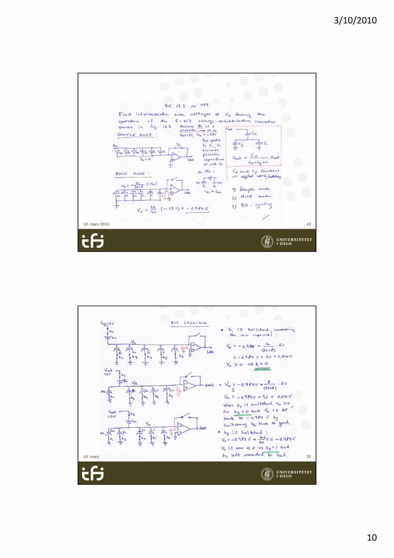
Charge-Redistribution A/D-Converter (unipolar)
• Instead of using a separate DAC and setting it equal to the input voltage (within 1input voltage (within 1 LSB) as for the DAC based converter from figure 13.5, one can use the error signal equaling the difference between the input signal, Vin, and the DAC output, VD/A
Numbers from 13.2 setting an error signal V equal to Vin – VD/A – modified succ. approx as in fig. 13.6

3/10/2010
9
Unipolar Charge-Redistribution A/D-Converter
CC2C4C8C16C
1. Sample mode
SAR
b1 b2 b3 b4 b5s
3
s2Vx 0
CC2C4C8C16C
2. Hold mode
SAR
SAR
s1
b1 b2 b3 b4 b5s
3
s1
s2
s2
Vx Vin–=
Vx Vin–Vref
2-----------+=
Vin Vref
Vin Vref
CC2C4C8C16C
3. Bit cycling
SAR
b1 b2 b3 b4 b5s3
s1Vin Vref
Charge-Redistribution A/D-Converter• Sample mode:
• All capacitors charged to Vin while the comparator is reset to its threshold voltage through S2. The capacitor array is performing S/H operation.
• Hold mode:• The comparator is taken out of reset by
opening S2, then all capacitors are switched to ground. Vx is now equal to –Vin. Finally S1 is switched so that Vref
can be applied to the capacitors during bit-cycling.
• Bit-cycling:• The largest capacitor is switched to
V V goes to V + V /2 If V isVref. Vx goes to –Vin + Vref/2. If Vx is negative, then Vin is greater than Vref/2 and the MSB capacitor is left connected to Vref. Otherwise the MSB capacitor is disconnected and the same procedure is repeated N times until the LSB capacitor has been evaluated.
3/10/2010
10
10. mars 2010 19
10. mars 2010 20
3/10/2010
11
10. mars 2010 21
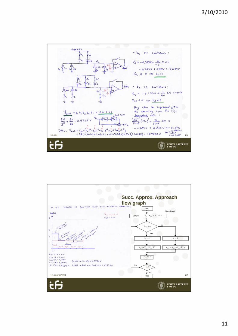
Succ. Approx. Approach flow graph
Sample
Start
Signed input
Vin
VD/A
, 0 i, 1= =
No
Yes
bi
1= bi
0=
Vin
VD/A
VD/A
VD/A
Vr ef
2 i 1++ VD/A
VD/A
Vr ef
2 i 1+ –
10. mars 2010 22Stop
No
Yes
i i 1+
i N

3/10/2010
12
Signed Charge redistribution A/D (Fig. 13.8)
• Resembling the unipolar version (Fig. 13.7)
• Assming Vin is between +/- Vref/2• Disadvantage: Vin attenuated by
a factor 2, making noise more of a problem for high resolution ADCs
• Any error in the MSB capacitorcauses both offset and a sign-causes both offset and a sign-dependent gain error, leading to INL errors
Resistor-Capacitor Hybrid (figure 13.9 in ”J & M”)• First all capacitors are charged to Vin
before the comparator is being reset.• Next a succ. approx. conversion is
performed to find the two adjacent resistor nodes having voltages larger and smaller than Vin
• One bus will be connected to one node while the other is connected to the other node. All of the capacitors are connected to the bus having the lower voltage.
• Then a successive approximationusing the capacitor-array network is done, starting with the largest capacitor…

3/10/2010
13
Speed estimate for charge-redistribution converters• RC time constants often limit speed• Individual time constant due to the
2C cap.: (Rs1+R+Rs2)2C • (R ; bit line)• Taueq=(Rs1+R+Rs2)2NC, for the
circuit in fig. 13.12• For better tha 0.5 LSB accuracy: e-
T/Taueq < 1/(2N+1), T = charging time• T > Taueq (N+1) ln2
= 0.69(N+1)Taueq
• 30 % higher than from Spice simulations (”J & M”)
Algorithmic (or Cyclic) A/D Converter (13.3) • Similar to the Successive
approximation converter• Constant Vref
• Doubles the error each cycle, Sample V = V
in, i = 1
StartSigned input
instead of halving the reference voltage in each cycle, like succ. approx. conv.
• Requires an accurate multiply-by-2 amplifier
• Accuracy can be improved by
V > 0
V 2(V – Vref /4) V 2(V + Vref /4)
No
Yes
bi
1= bi
0=
• Accuracy can be improved by operating in four cycles (instead of two)
• compact
i i + 1
i > N
Stop
No
Yes

3/10/2010
14
Ratio-Independent Algorithmic Converter
S/H CmpVin
Shift register
Out
• Simple circuitry
S/HX2Vref /4
–Vref /4Gain amp
• Due to the cyclic operation the circuitry are reused in time
• Fully differential circuits normally used
Ratio-Independent Algorithmic Converter
CmpVerr
C1
Q1
C2
1. Sample remainder and cancel input-offset voltage.
CmpVerr
C1
Q1
C2
2. Transfer charge Q1 from C1 to C2.
Q1
• The basic idea is to sample the input signal twice using the same capacitor. During the 2nd sampling the charge from the 1st capacitor is stored on a 2nd
CmpVerr
C1
Q2
C2
3. Sample input signal with C1 again
Q1
CmpVerr
C1
Q1+Q2
C2
4. Combine Q1 and Q2 on C1, and connect C1 to output.
Vout = 2 Verr
after storing charge Q1 on C2.
During the 2nd sampling the charge from the 1st capacitor is stored on a 2nd
capacitor whose size is unimportant. After the 2nd sampling both charges are recombined into the 1st capacitor which is then connected between the opamp input and output.
• Does not rely on capacitor matching, is insensitive to amplifier offset.
3/10/2010
15
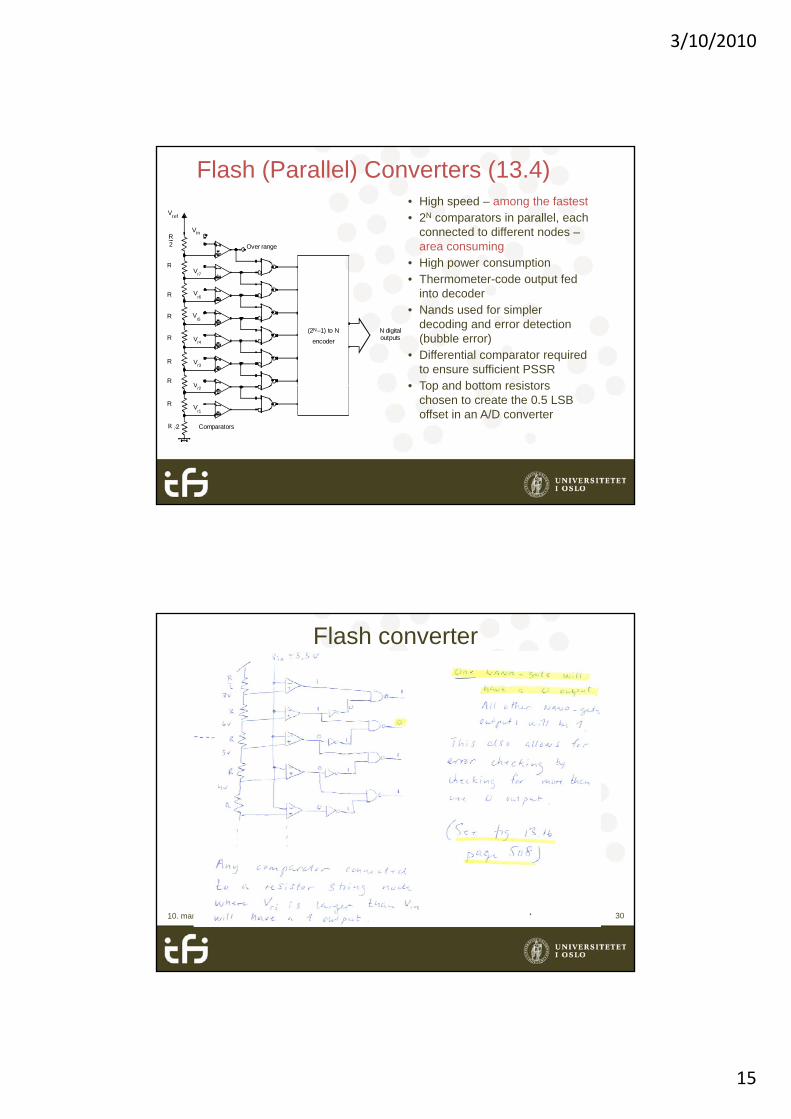
Flash (Parallel) Converters (13.4)• High speed – among the fastest• 2N comparators in parallel, each
connected to different nodes –area consuming
• High power consumption
Vref
Vin
Over range
R
R2----
High power consumption• Thermometer-code output fed
into decoder• Nands used for simpler
decoding and error detection (bubble error)
• Differential comparator required to ensure sufficient PSSR
• Top and bottom resistors
(2N–1) to N
encoder
N digitaloutputs
R
R
R
R
R
R
V
Vr3
Vr4
Vr5
Vr6
Vr7
• Top and bottom resistors chosen to create the 0.5 LSB offset in an A/D converter
Comparators
R Vr1
Vr2
R 2
Flash converter
10. mars 2010 30
3/10/2010
16
Clocked CMOS comparator
• When the clock (”phi”) is high, the inverter is set to its bistable point, Vin = Vout (= Vdd/2). The other (left) side of C is charged to Vri.
• When the clock (”phi”) goes low, the inverter switches, depending on the voltage differencebetween Vri and Vin. (Vri > Vin; 1 output, Vri < Vin; 0 output from inv. )
• Differential inverters helps poor PSRR with this simple comparator solution.
Issues in Designing Flash A/D Converters• Input Capacitive Loading: The large number of comparators connected to
Vin results in a large capacitive load on at the input node which increases power and reduces speed
• Comparator Latch-to-Track Delay: The internal delay in the comparator when going from latch to track mode
• Signal and/or Clock Delay: Differences in signal/clock delay between the g y g ycomparators may cause errors. Example: A250-MHz, 1-V peak input-sinusoid converted with 8-bit resolution requires a precision of 5ps. Can be reduced by matching the delays and capacitive loads on the signal/clock.
• Substrate and Power-Supply Noise: For a 8-bit converter with Vref=2V only 7.8mV of noise injection is required to introduce an error of 1LSB. The problem can be reduced by proper layout (Shielding, Differential clocks, Separate power supplies, and symmetrical layout)
• Bubble Error Removal: Comparator metastability may introduce wrong p y y gthermometer code ( a single 1 or 0 in between opposite values)
• Flashback: Caused by latched comparators. When the comparator is switched from track to latch mode a charge glitch is introduced at the input. The problem is reduced by using a preamplifier and input impedance matching

3/10/2010
17
Two-Step (Subranging) A/D Converters (13.5)
4-bit
A/D
4-bitD/A 16Vin
Gain amp
V1
Vin
VqMSB
4-bit
A/DLSB
• Popular choice for high-speed medium accuracy converters (8-10 b)• Less area and power consumption than a Flash ADC
First 4 bits
Gain amp
Lower 4 bitsb1 b2 b3 b4, , , b5 b6 b7 b8, , ,
• The MSB’s are converted during the first step. In the next step the remaining error is converted into the LSB’s
• Speed is limited by the Gain Amplifier• Requires N-bit accuracy for all components (May be relaxed by
using Digital Error Correction)
Digital Error Correction for two-step A/D
S/H14-bit
S/H2
4-bitD/A 8 S/H3Vi
Gain amp
(8-bit accurate)
V1
Vin
VqMSBS/H1A/D
D/A 8 S/H3
ErrorcorrectionD
Digital delay
4 bits
5 bits
Vin
(4-bit accurate)(8-bit accurate)
(5-bit accurate)
(5-bit accurate)
(8-bit accurate)
MSB
5-bit
A/DLSB
• The accuracy requirements on the input ADC is relaxed due to the error corr.. 4-bit for MSb converter (not 8-bit).
8 bits

3/10/2010
18
Pipelined ADCs (13.5) Once the first stage has completed it’s work it immediately starts working on the next sample
• Small area
b
D 1
Q 1
DN -2
Q N- 1
D N
Q N
D 1
Q 1
D1
Q 1
D N -2
Q N -1
1-b itD A P R X
1 -b itDA P R X
1-b itD A P RX
1 -b itDA P R X
V in
N –
1-b
it sh
ift r
egi
ste
r
(D A P RX d ig ita l ap p rox im a to r)
b1
b2
b N
b N 1–
A n a lo g p ip e lin e(D A P RX - d ig ita l ap p rox im a to r)
S /H
2
Cm p
–V re f/4
V re f/4
V i– 1
V i
b i
Pipelined ADC -example
3/10/2010
19
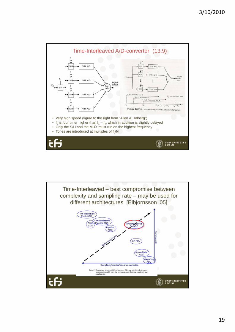
Time-Interleaved A/D-converter (13.9)
S/H N-bit A/D
f2
f1
f
S/H
S/H
S/H
S/H
N-bit A/D
N-bit A/D
N-bit A/D
Dig.mux
Digitaloutput
f3
f4
f0
Vin
• Very high speed (figure to the right from “Allen & Holberg”)• f0 is four timer higher than f1 – f4, which in addition is slightly delayed• Only the S/H and the MUX must run on the highest frequency• Tones are introduced at multiples of f0/N
Time-Interleaved – best compromise between complexity and sampling rate – may be used for
different architectures [Elbjornsson ’05]

3/10/2010
20
Dynamic range
• Dynamic range is defined as the power of the maximum input signal range divided by the total power of the quantization noise and distortionpower of the quantization noise and distortion
• Often referred to as Signal-to-Noise-and-Distortion range
• S/(N+D)• SINAD
Analog and digital supply voltages are reduced as technology scales
Some ADC trends:
• Limited dynamic range at low supply voltages remains the utmost challenge for high-resolution Nyquist converters.
• Oversampling converters will dominate this arena in the future
• Linearity correction with• Linearity correction with digital correction is becoming prevalent
10. mars 2010 40

3/10/2010
21
Nyquist ADCs at ISSCC; FOM, Effective Number of Bits
• FOM: Figure of Merit• High-resolution conv.:
FOM minimum at about 10-17J/step6 bit ADC FOM b t 4• 6-bit ADCs : FOM about 4 orders of magnitude worse than 14 bit converters, suggesting that there is much to be gained by designing more effecient 6-bit ADCs
• Better ENOB reported forBetter ENOB reported for 350 nm than 250 nm, 180 nm and 130 nm
• Data from ISSCC up to 2005.10. mars 2010 41
Nyquist ADCs at ISSCC; FOM, Sampling rate
• Maximum Sampling frequency (Usually faster is better) and FOMFOM.
• ISSCC 2000-2007 (90 nm, 130 nm, 180 nm technologies)
• Small improvement in sampling frequency in going to finergoing to finer technologies, mainly due to reduced capacitance.10. mars 2010 42

3/10/2010
22
Publicationyear
SFDR@Nyquist [dB]
ENOB @ Nyquist
Nyquistupdaterate,[Ms/s]
Power consumpt.[mW]
Area[mm2]
Supplyvoltage[V]
Technology[nm]
other Reference
2006 55 8.5 1000 250 3.5 1.2 130 Time interleaved
Gupta et al IEEE JSSC ’06
2007 4 2500 24 0.057 1.2 130 ”Pipelinedflash”
Wang et al, IEEE Trans. Instr. Meas.
2007 5 500 6 0.9 1.2 65Time interleavedsucc. approx
Ginsburg et al IEEE JSSC ’07
2007 8 100 30 2.04 1.0 180Switchedopamppipelined
Wu et al, IEEE JSSC ’07
2008 10 30 22 0.7 1.8 180pipelined Li et al, IEEE
JSSC ’08
2009 81 13 0.073 0.7 180Delta‐sigma Chae, JSSCC
Feb.09
2009 27 5 4 3 1750 2 2 0 02 1 0 90”folding flash” Verbruggen,
JSSCC Mar ’092009 27.5 4.3 1750 2.2 0.02 1.0 90 JSSCC,Mar. ’09
2009 10 1.2 12.2 0.354 3.3 350Continous time sigma delta
TCAS‐II, Jan. ’09
10. mars 2010 43
Sampling-time uncertainty
VinVref
2---------- 2fint sin=
•Variation in output voltage caused by variations in the time of sampling
Consider the following input signal:
tVLSB
fi V f--------------------
1
2N
f----------------=
tIf the variation in sampling time is , following equation must be satisfied to keep less than 1LSBV
finVref 2Nfin
3/10/2010
23
Additional litterature• Phillip E. Allen, Douglas Holberg: CMOS Analog Circuit Design, Holt Rinehart Winston, 1987.
• Jonas Elbornsson: White paper on parallel successive approximation ADC, Mathcore Engineering AB, 2005.
• R. Gregorian, G. Temes: Analog MOS Integrated Circuits for Signal Processing, Wiley, 1986
• D. M.Gingrich Lecture Notes, University of Alberta, CanadaD. M.Gingrich Lecture Notes, University of Alberta, Canada http://www.piclist.com/images/ca/ualberta/phys/www/http/~gingrich/phys395/notes/phys395.html
• Walt Kester: Which ADC is right for your application?
• Y. Chiu, B. Nicolic, P. R. Gray: Scaling of Analog-to-Digital Converters into Ultra-Deep-Submicron CMOS, Proceedings of Custom Integrated Circuits Conference, 2005.
• Lecture Notes, University of California, Berkeley,
EE247 Analog Digital Interface Integrated Circuits, Fall 07;http://inst.eecs.berkeley.edu/~ee247/fa07/
• Lanny L. Lewyn, Trond Ytterdal, Carsten Wulff, Kenneth Martin: ”Analog Circuit Design in Nanoscale CMOS Technologies”, Proceedings of the IEEE, October 2009.
• James L. McCreary, Paul R. Gray: ”All-MOS Charge Redistribution Analog-to-Digital Conversion Techniques part 1” IEEE Journal of Solid State circuits December 1975Techniques – part 1 , IEEE Journal of Solid-State circuits, December 1975.
Next Tuesday (10/3-08):Rest of chapter 13.
• Chapter 14 Oversampling Converters

3/10/2010
24
Analog Layout - mismatch
• ”…The ratio between two similar components on the same integrated circuit can be controlled to better than +/- 1 % and in many cases tocircuit can be controlled to better than +/ 1 %, and in many cases, to better than +/- 0.1 %. Devices specifically constructed to obtain a known, constant ratio are called matched devices.”
• ”Matching – the Achilles Heel of Analog” (Chris Diorio)10. mars 2010 47
Some companies located in Norway, doing (or that have done) full custom data converter designs:
• Analog Concepts (Trondheim)• Arctic Silicon Devices (Trondheim)• Atmel Norway (Trondheim)• Energy Micro (Oslo)• GE Vingmed Ultrasound (Horten)• Nordic Semiconductors (Trondheim,
Oslo)• Novelda (Oslo)• Micrel (Oslo)( )• Sintef (Trondheim, Oslo)• Texas Instruments (Oslo)
10. mars 2010 48

3/10/2010
25
Metastability in FFs ( http://www.asic-world.com/tidbits/metastablity.html ) To avoid M. in comparators: Make gain high, increase current levels.
10. mars 2010 49