LASER World of Photonics 2017
20
LASER World of Photonics 2017 The Berlin Brandenburg Pavilion
Transcript of LASER World of Photonics 2017

LASER World of Photonics 2017The Berlin Brandenburg Pavilion

Berlin Brandenburg Pavilion

SLT - Sensor- und Lasertechnik GmbHPaul-Drude-Institut für FestkörperelektronikOsTech e.K.Berlin Adlershof - WISTA-MANAGEMENT GMBHFraunhofer Heinrich Hertz InstituteUNI Potsdam, Leibniz-Institut für Astrophysik Potsdam (AIP)SENTECH Instruments GmbHFerdinand-Braun-Institut,Leibniz-Inst. f. HöchstfrequenztechnikAdvanced UV for LifeTU Berlin - Institut für Optik und atomare PhysikAdlOptica GmbH
Photonics Cluster Berlin Brandenburg OpTecBB e.V.
NetworkingLaserverbund Berlin-Brandenburg e.V.
Hall B2, Booth 350
1
3
2
4 i 5
6
7
8
91011
N
12
34
56
78
910
11
(i)nfo
NN

(10 universities and 26 extra-university research institutions) and the high amount of specialized small and medium-sized companies (overall 390 SMEs) with widely ranged know-how – a perfect basis for a mutual transfer between science and in-dustry leading to national and international cooperation.
Optical Technologies and Microsystems Technology – Future Key TechnologiesIn order to further promote the tech- nological development of the region the Cluster Photonics was built. It provides companies and research institutions access to resources, such as knowledge and capital, at both local and international level in the fields of:• Laser Technology• Lighting Technology• Optics for Communication and
Sensors• Optical Analytics• Biomedical and Ophthalmic Optics• Microsystems TechnologyThe Photonics Cluster in Berlin and Brandenburg is especially distinguished by the strong scientific basis
c/o Berlin Partner für Wirtschaft und Technologie GmbHFasanenstr. 8510623 Berlin, Germany
Gerrit Rösslerfon: +49 30 46302-500
Photonics Cluster Berlin-Brandenburg

AdlOptica GmbH works in field of refractive Multi-Focus and Laser Beam Shaping Optics finding applications in numerous industrial and scientific techniques. Result of multi year developments is realized in families of piShaper and foXXus systems numbering today more than 60 models: almost 100% efficiency, spectrum from UV to IR, power from mW to kW, CW and pulse lasers, achromatic design, wide range of flattop spot sizes, low sensitivity to misalignment. AdlOptica is locating in Adlershof, Berlin, Germany‘s leading science and technology park.
Rudower Chaussee 2912489 Berlin, Germany
Dr. Alexander Laskinfon: +49 30 565908880fax: +49 30 565908881
AdlOptica GmbH

application of UV LEDs.The consortium provides:• a strong network for the development
of custom-tailored UV LEDs,• the whole value chain: from material
through UV LEDs and UV photo-detectors, modules and systems to final applications,
• worldwide acknowledged know-how in photonics, medicine, plant growth, water treatment, production and materials engineering. Advanced UV for Life is funded by the German Federal Ministry of Education and Research within the program „Twenty20 –Partnership for Innovation“.
Advanced UV for Life ist ein Bündnis aus Unternehmen und Forschungseinrichtugen, die UV-LEDs und darauf basierende Anwendungen entwickeln.Das Konsortium bietet:• ein starkes Netzwerk für die Ent-
wicklung von maßgeschneiderten UV-LEDs,
• die komplette Wertschöpfungskette – vom Material über UV-LEDs und UV-Photodetektoren sowie Module und Systeme bis hin zur Anwendung,
• weltweit anerkanntes Know-how in Photonik, Medizin, Pflanzenwachs-tum, Wasserbehandlung, Produktion und Materialentwicklung.
Advanced UV for Life wird vom BMBF im Rahmen des Programms „Zwanzig20 – Partnerschaft für Innovation“ gefördert.Advanced UV for Life is a consortium of industrial companies and academic institutions operating in development and
c/o Ferdinand-Braun-Institut, Leibniz-Institut für HöchstfrequenztechnikGustav-Kirchhoff-Straße 412489 Berlin, Germany
Antje Mertschfon: +49 30 6392-3397fax: +49 30 6392-3392
Advanced UV for Life

A leader in Photonics, Optics and Micro Systems:The Berlin-Brandenburg region is home to one of the most significant clusters for optics technologies in Europe. Many of these businesses are based at Adlershof, in the Photonics Centre’s six buildings, which comprise 18,600 square metres of lab and office spaces. Companies such as Analytik Jena, FISBA Optik, Limmer Laser, AEMtec, Bestec, Bruker nano, Jenoptic Diode Lab, Laser Technik Berlin (LTB), LLA Instruments oder Sentech are situated in Adlershof.
Adlershof ist führend in Photonik, Optik und Mikrosystemtechnik:Berlin-Brandenburg ist eines der stärksten Cluster der Photonik, Optik und Mikrosys-teme in Europa. Zahlreiche Unternehmen aus diesen Bereichen haben ihren Sitz im Technologiepark Adlershof u.a. in den sechs Gebäuden des Photonikzentrums (ZPO) mit rund 18.600 m² Labor-, Hallen- und Büroflächen. Hier siedeln u.a. Firmen wie Analytik Jena, FISBA Optik oder Lim-mer Laser. Etliche Firmen sind dem ZPO bereits entwachsen und haben in Adlershof ihr eigenes Gebäude gebaut wie AEMtec, Bestec, Bruker nano, Jenoptic Diode Lab, Laser Technik Berlin (LTB), LLA Instru-ments oder Sentech.
Rudower Chaussee 17 12489 Berlin, Germany
Sandra Chabrierfon: +49 30 63922250fax: +49 30 63922235
Berlin Adlershof – WISTA-MANAGEMENT GMBH

Kurzpulslaser mit GaN-Transistoren zur An- steuerung für Anwendungen wie LIDAR.Short-pulse laser with GaN transistors as driver for applications such as LIDAR.
Das FBH präsentiert das komplette Spektrum seiner Diodenlaser, vom Chip bis zum fertigen System – darunter seine flexible All-in-One Pulslaserquelle. Sie liefert optische ps-Pulse mit nJ-Energien bei Wiederholfrequenzen vom kHz- bis in den MHz-Bereich. Zudem bietet das Institut die volle Technologiekette bei UV-LEDs von 260-320 nm.
The FBH presents the complete spectrum of its diode lasers, from the chip to the final system – including its flexible All-in-One pulse laser source, delivering optical ps pulses with nJ energies at repetition frequencies between kHz and MHz. Moreover, the institute offers the full UV-LED technology chain from 260-320 nm.
Gustav-Kirchhoff-Str. 412489 Berlin, Germany
Petra Immerzfon: +49 30 6392-2626fax: +49 30 6392-2602
„partner in Advanced UV for Life“
Ferdinand-Braun-Institut, Leibniz-Institut für Höchstfrequenztechnik
©FB
H/s
chur
ian.
com

„From optical sensing to information technology – this is the range of solutions developed at the HHI. Under ISO 9001, we design photonic networks and systems and fabricate different types of semiconductor lasers, LEDs, photodiodes, novel InP based THz devices for simpler solutions for the THz technology, microring resonators for environmental and medical sensing applications, DOEs as well as polymer OEICs in HHI’s PolyBoard platform. In addition, HHI offers high-end measure-ment, system test-beds, component test and qualification facilities as well as InP epitaxial and foundry services.”
Einsteinufer 3710587 Berlin, Germany
Jörn Falkfon: +49 30 31002 275
Fraunhofer Heinrich Hertz Institute

(companies, universities, research institutions and associations). We have established ourselves in 1993 and today count more than 120 members.
Our services:- Workshops, seminars and user groups- Communication of advanced training courses and consulting services- Regular informal gatherings to discuss laser technology issues- Networking from a pool of professionals and skilled personnel
Wir - der Laserverbund Berlin-Brandenburg e.V. - sind der Zusammenschluss von Fachleuten aus Wirtschaft und Forschung auf dem Gebiet der Lasertechnik und Laser- anwendung mit über 120 Mitgliedern.
Unsere Angebote:- Workshops, Seminare und Anwender treffen- Vermittlung von Weiterbildungsan- geboten- Regelmäßiger Laserstammtisch- Vermittlung von Beratungsleistungen- Fachkräftepool
We - the Berlin-Brandenburg Laser Associ-ation e.V. - are an association of pro-fessionals from business and research
c/o Stumhöfer GmbH doreum luxLessingstraße 1616356 Ahrensfelde-Berlin, Germany
Prof. Dr. Eberhard Stensfon: +49 30 99 272 400fax: +49 30 99 272 401
Laserverbund Berlin-Brandenburg e.V.

Optec-Berlin-Brandenburg e.V. is the competence network for optical tech-nologies and micro-system technology in the region of Berlin-Brandenburg. OpTecBB is an initiative of companies and scientific institutions in Berlin-Brandenburg who aim to explore and use the technology together. OpTecBB was founded on Sep-tember 14th, 2000 by companies, research institutions, universities and federations supported by relevant ministries in Bran-denburg and the Berlin Senate. Today, the association has approximately 110 institutional employees.
Optec-Berlin-Brandenburg (OpTecBB) e.V. ist das Kompetenznetz für Optische Tech-nologien und Mikrosystemtechnik in den Ländern Berlin und Brandenburg. OpTecBB e.V. ist eine Initiative von Unternehmen und wissenschaftlichen Einrichtungen in Berlin und Brandenburg, die gemeinsame Wege zur Erschließung und Nutzung dieser Technologien gehen wollen. OpTecBB e.V. wurde am 14.9.2000 von Unternehmen, Forschungseinrichtungen, Universitäten und Verbänden mit Unterstützung der zuständigen Landesministerien Brandenburgs und des Senats von Berlin gegründet. Heute hat der Verein ca. 110 institutionelle Mitglieder.
Rudower Chaussee 2512489 Berlin, Germany
Dr. Frank Lerchfon: +49 30 6392 1720fax: +49 30 6392 1729
OpTecBB e.V.

Entwicklung und Fertigung von Laser-treibern, TEC-Reglern und Diodenlaser-sytemen. CW-Modus oder Pulsmodi, analoge oder digitale Modulation. Schnelle kundenspezifische Anpassungen, Industrie- und Medizin-Geräte.
Design and production of laser drivers, TEC controllers and diode laser systems. CW, QCW, analog and digital control options. Fast adaption to customer requirements, industrial and medical devices.
Boxhagener Str. 76-7810245 Berlin, Germany
Herr Oswaldfon: +49 30 2977304-0fax: +49 30 2977304-11
OsTech GmbH e.K.
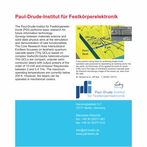
A two-section cavity laser for achieving single-mode operation was produced by separating an existing cavity into two parts. (a) Schematic of the applied focused ion beam (FIB) cut to the ridge of a terahertz quantum-cascade laser. (b) Electron microscopy image of the actual cut, seen from the side. M. Hempel et al., AIP Adv. 7, 055201 (2017).
The Paul-Drude-Institut für Festkörperelek-tronik (PDI) performs basic research for future information technology. Synergy between materials science and solid state physics aims at the stimulation and demonstration of new functionalities. The Core Research Area Intersubband Emitters focusses on terahertz quantum-cascade lasers (THz QCLs) based on complex GaAs/(Al,Ga)As heterostructures. THz QCLs are compact, unipolar semi-conductor lasers with output powers of the order of 10 mW and emission frequencies between 2 and 5.4 THz. The maximum operating temperatures are currently below 200 K. However, the lasers can be operated in mechanical coolers.
Hausvogteiplatz 5-710117 Berlin, Germany
Mercedes Reischelfon: +49 30 20377-481fax: +49 30 20377-515
Paul-Drude-Institut für Festkörperelektronik
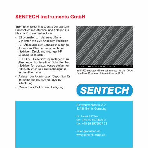
In SI 500 geätztes Gitterspektrometer für den GAIA Satelliten (Courtesy Universität Jena, IAP)
SENTECH fertigt Messgeräte zur optische Dünnschichtmesstechnik und Anlagen zur Plasma Prozess Technologie • Ellipsometer zur Messung dünner Schichten mit Sub-Angström Präzision• ICP Ätzanlage zum schädigungsarmen Ätzen, das Plasma brennt auch bei niedrigem Druck und niedriger HF Leistung noch stabil• IC PECVD Beschichtungsanlagen zum Abscheiden hochwertiger Schichten bei niedriger Temperatur, wasserstoffarmen Nitridschichten und zum schädigungs- armen Abscheiden.• Anlagen zur Atomic Layer Deposition für 3d konforme und hochgenaue Be- schichtung• Clustertools für F&E und Fertigung
Schwarzschildstraße 212489 Berlin, Germany
Dr. Helmut Witekfon: +49 89 8979607 0fax: +49 89 8979607 22
SENTECH Instruments GmbH
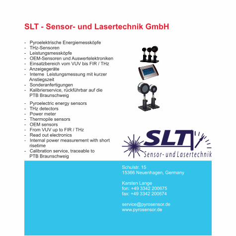
- Pyroelektrische Energiemessköpfe- THz-Sensoren- Leistungsmessköpfe- OEM-Sensoren und Auswertelektroniken- Einsatzbereich vom VUV bis FIR / THz- Anzeigegeräte- Interne Leistungsmessung mit kurzer Anstiegszeit- Sonderanfertigungen- Kalibrierservice, rückführbar auf die PTB Braunschweig
- Pyroelectric energy sensors- THz detectors- Power meter- Thermopile sensors- OEM sensors- From VUV up to FIR / THz- Read out electronics- Internal power measurement with short risetime- Calibration service, traceable to PTB Braunschweig
Schulstr. 1515366 Neuenhagen, Germany
Karsten Langefon: +49 3342 200675fax: +49 3342 200674
SLT - Sensor- und Lasertechnik GmbH
Information Technology Solutions
�

The laser group at the Institute of Optics and Atomic Physics at the TU Berlin has advanced expertise in manufacturing die-lectric thin films on glasses and fibre end faces. Currently, steep edge filters are being pro-duced on fiber end faces with the help of „ion-assisted-deposition“ having up to 72 layers. These filters were designed to ma-nufacture small Raman fiber probes having an outside diameter of 1.5 mm. The Raman fibre probe was being integrated in a Ra-man diagnostic setup build by the TU Berlin which is smaller than an A4 paper and a few centimeters high.
Raman-Diagnostik & Herstellung optischer Filter auf Glasfaserendflächen
Die Lasergruppe am Institut für Optik und Atomare Physik an der TU Berlin besitzt fortgeschrittenes Know-how in der Her-stellung von dielektrischen Dünnschicht-systemen auf Gläsern und Glasfaserend-flächen.Derzeit werden scharfe Kantenfilter mit der „ion-assisted-deposition“ auf Glaserfase-rendflächen hergestellt, sogenannte „steep-edge“ Filter mit bis zu 72 Schichten. Diese Filter ermöglichen den Aufbau von bis zu 1,5 mm dünnen Raman-Fasersonden und kommen in einer äußerst kompakten Raman-Diagnoseeinheit zum Einsatz. Die von der TU Berlin entwickelte Raman-Diagnoseeinheit ist kleiner als ein A4 Blatt und nur wenige Zentimeter hoch.
Manufacturing of optical filters on fiber end faces
Institut für Optik und Atomare PhysikAG Woggon/EichlerStraße des 17. Juni 135, Sekr. ER1-110623 Berlin, Germany
M.Eng. Christian Nitschkefon: +49 30 314-22449
Technische Universität Berlin, Institut für Optik und atomare Physik

hours. A radical decrease in measurement time can be achieved by applying fiber bundle-coupled multiplex spectrographs usually used in astronomy. They are de-signed for recording thousands of spatially resolved spectra of a two-dimensional image field within one single exposure. Transferring this technology to imaging Raman spectroscopy allows a considerably faster acquisition of chemical maps. This is of particular interest for medical diagnostics, e.g. the identification of abnormalities of skin tissue.
Übliche bildgebende Ramanspektrogra-phen tasten eine Probe zeitaufwändig ab. Selbst bei nur 100 Bildpunkten beträgt die Messzeit Minuten oder gar Stunden. Eine drastische Verkürzung der Messdauer lässt sich mit faserbündelgekoppelten Astrono-miespektrographen erzielen, die in einem einzigen Belichtungsvorgang ortsaufgelöste Spektren eines zweidimensionalen Bildfel-des aufnehmen. Eine Übertragung dieser Technologie in die bildgebende Ramanspektroskopie ermöglicht eine deutlich schnellere Erstellung chemischer Karten. Diese Technik ist besonders inter-essant für die medizinische Diagnostik, z.B. für die Identifizierung von krebsverdächti-gem Hautgewebe.
Time-consuming scanning of samples is still common in imaging Raman spectros-copy. Even for just 100 image points the testing time may add up to minutes or
An der Sternwarte 1614482 Potsdam, Germany
Dr. Elmar Schmälzlinfon: +49 331 7499 638fax: +49 331 7499 436
Leibniz-Institut für Astrophysik Potsdam (AIP)

Notizen / Notes:
managed by:
Fasanenstr. 8510623 Berlin, GermanyMr. Olav Morales Klugefon: +49 30 46302 – [email protected]
The joint presentation of the German Capital Region Berlin-Brandenburg is hosted by the local economic authority of the state of Berlin:
supported by: