Design of a Neural Network Based Optical Character Recognition

Large-Scale Optical Neural Networks Based on Photoelectric Multiplication
Ryan Hamerly,* Liane Bernstein, Alexander Sludds, Marin Soljačić, and Dirk EnglundResearch Laboratory of Electronics, MIT, 50 Vassar Street, Cambridge, Massachusetts 02139, USA
(Received 12 November 2018; revised manuscript received 21 February 2019; published 16 May 2019)
Recent success in deep neural networks has generated strong interest in hardware accelerators toimprove speed and energy consumption. This paper presents a new type of photonic accelerator based oncoherent detection that is scalable to large (N ≳ 106) networks and can be operated at high (gigahertz)speeds and very low (subattojoule) energies per multiply and accumulate (MAC), using the massive spatialmultiplexing enabled by standard free-space optical components. In contrast to previous approaches, bothweights and inputs are optically encoded so that the network can be reprogrammed and trained on the fly.Simulations of the network using models for digit and image classification reveal a “standard quantumlimit” for optical neural networks, set by photodetector shot noise. This bound, which can be as low as50 zJ=MAC, suggests that performance below the thermodynamic (Landauer) limit for digital irreversiblecomputation is theoretically possible in this device. The proposed accelerator can implement both fullyconnected and convolutional networks. We also present a scheme for backpropagation and training that canbe performed in the same hardware. This architecture will enable a new class of ultralow-energy processorsfor deep learning.
DOI: 10.1103/PhysRevX.9.021032 Subject Areas: Interdisciplinary Physics,Optoelectronics, Photonics
I. INTRODUCTION
In recent years, deep neural networks have tackled awide range of problems including image analysis [1],natural language processing [2], game playing [3], physicalchemistry [4], and medicine [5]. This is not a new field,however. The theoretical tools underpinning deep learninghave been around for several decades [6–8]; the recentresurgence is driven primarily by (1) the availability oflarge training datasets [9] and (2) substantial growth incomputing power [10] and the ability to train networks ongraphics processing units (GPUs) [11]. Moving to morecomplex problems and higher network accuracies requireslarger and deeper neural networks, which in turn requireeven more computing power [12]. This motivates thedevelopment of special-purpose hardware optimized toperform neural-network inference and training [13].To outperform a GPU, a neural-network accelerator
must significantly lower the energy consumption, sincethe performance of modern microprocessors is limited byon-chip power [14]. In addition, the system must be fast,programmable, scalable to many neurons, compact, and
ideally compatible with training as well as inference.Application-specific integrated circuits (ASICs) are oneobvious candidate for this task. State-of-the-art ASICscan reduce the energy per multiply and accumulate(MAC) from 20 pJ=MAC for modern GPUs [15] to around1 pJ=MAC [16,17]. However, ASICs are based on CMOStechnology and therefore suffer from the interconnectproblem—even in highly optimized architectures wheredata are stored in register files close to the logic units, amajority of the energy consumption comes from datamovement, not logic [13,16]. Analog crossbar arrays basedon CMOS gates [18] or memristors [19,20] promise betterperformance, but as analog electronic devices, they sufferfrom calibration issues and limited accuracy [21].Photonic approaches can greatly reduce both the logic
and data-movement energy by performing (the linear partof) each neural-network layer in a passive, linear opticalcircuit. This allows the linear step to be performed at highspeed with no energy consumption beyond transmitterand receiver energies. Optical neural networks based onfree-space diffraction [22] have been reported, but requirespatial light modulators or 3D-printed diffractive ele-ments, and are therefore not rapidly programmable.Nanophotonic circuits are a promising alternative[23,24], but the footprint of directional couplers andphase modulators makes scaling to large (N ≥ 1000)numbers of neurons very challenging. To date, the goalof a large-scale, rapidly reprogrammable photonic neuralnetwork remains unrealized.
Published by the American Physical Society under the terms ofthe Creative Commons Attribution 4.0 International license.Further distribution of this work must maintain attribution tothe author(s) and the published article’s title, journal citation,and DOI.
PHYSICAL REVIEW X 9, 021032 (2019)
2160-3308=19=9(2)=021032(12) 021032-1 Published by the American Physical Society

This paper presents a new architecture based on coherent(homodyne) detection that is fast, low power, compact,and readily scalable to large (N ≳ 106) numbers of neurons.In contrast to previous schemes, here we encode both theinputs and weights in optical signals, allowing the weightsto be changed on the fly at high speed. Synaptic con-nections (matrix-vector products) are realized by thequantum photoelectric multiplication process in the homo-dyne detectors. Our system is naturally adapted to free-space optics and can therefore take advantage of themassive spatial multiplexing possible in free-space systems[25,26] and the high pixel density of modern focal-planearrays [27] to scale to far more neurons than can besupported in nanophotonics or electronic crossbar arrays.The optical energy consumption is subject to a fundamentalstandard quantum limit (SQL) arising from the effects ofshot noise in photodetectors, which lead to classificationerrors. Simulations based on neural networks trained onthe Modified NIST (MNIST) dataset [8] empirically showthe SQL can be as low as 50–100 zeptojoules ðzJÞ=MAC.Using realistic laser, modulator, and detector energies,performance at the sub-fJ/MAC level should be possible
with present technology. The optical system can be used forboth fully connected and convolutional layers. Finally,backpropagation is straightforward to implement in oursystem, allowing both inference and training to be per-formed in the same optical device.
II. COHERENT MATRIX MULTIPLIER
Figure 1 illustrates the device. A deep neural network is asequence ofK layers [Fig. 1(a)], each consisting of a matrixmultiplication x → Ax (synaptic connections) and an ele-mentwise nonlinearity xi → fðxiÞ (activation function);thus the input into the (kþ 1)th layer is related to thekth layer input by
xðkþ1Þi ¼ f
�Xj
AðkÞij x
ðkÞj
�: ð1Þ
For a given layer, let N and N0 be the number of inputand output neurons, respectively. Input (output) data areencoded temporally as N (N0) pulses on a single channelas shown in Fig. 1(b). This encoding, reminiscent of
(a)
(b)
OO E
I
W
FIG. 1. Schematic diagram of a single layer of the homodyne optical neural network. (a) Neural network represented as a sequence ofK layers, each consisting of a matrix-vector multiplication (gray) and an elementwise nonlinearity (red). (b) Implementation of a singlelayer. Matrix multiplication is performed by combining input and weight signals and performing balanced homodyne detection (inset)between each signal-weight pair (gray box). For details on experimental implementation see Sec. S1 of Supplemental Material [31]. Theresulting electronic signals are sent through a nonlinear function (red box), serialized, and sent to the input of the next layer.
RYAN HAMERLY et al. PHYS. REV. X 9, 021032 (2019)
021032-2

the coherent Ising machine [28–30], contrasts with otherapproaches used for neural networks, which encode inputsin separate spatial channels [22–24]. As there are NN0weights for an N0 × N fully connected matrix, the weightsenter on N0 separate channels, each carrying a single matrixrow encoded in time. Input data are optically fanned out toall N0 channels, and each detector functions as a quantumphotoelectric multiplier, calculating the homodyne productbetween the two signals [inset of Fig. 1(b)]. As long as bothsignals are driven from the same coherent source and thepath-length difference is less than the coherence length, thecharge Qi accumulated by homodyne receiver i is
Qi ¼2ηeℏω
ZRe½EðinÞðtÞ�EðwtÞ
i ðtÞ�dt ∝Xj
Aijxj: ð2Þ
Here EðinÞðtÞ and EðwtÞi ðtÞ are the input and weight fields for
receiver i, which are taken to be sequences of pulses withamplitudes proportional to xj and Aij, respectively (xj,Aij ∈ R). Thus, each receiver performs a vector-vector
product between x and a row Ai of the weight matrix; takentogether, the N0 electronic outputs give the matrix-vectorproduct Ax. Fields are normalized so that power is given byPðtÞ ¼ jEðtÞj2, and η is the detector efficiency. A serializerreads out these values one by one, applies the nonlinearfunction fð·Þ in the electrical domain, and outputs the resultto a modulator to produce the next layer’s inputs.The balanced homodyne detector in Fig. 1(b) (inset)
combines the advantages of optics and electronics: it canprocess data encoded at extremely high speeds, limitedonly by the bandwidth of the beam splitter (≳THz) and the(optical) bandwidth of the photodetectors (typically≳100 nm, or ≳10 THz). The electrical bandwidth canbe much slower, since only the integrated charge ismeasured. Finally, the present scheme avoids the needfor low-power nonlinear optics that is a major stumblingblock in all-optical logic [32]: since the output is electrical,the dot product Aijxj can be computed at extremely lowpower (sub-fJ/MAC) using standard nonresonant compo-nents (photodiodes) that are CMOS compatible and scal-able to arrays of millions.Previous approaches used optoelectronics (photodiodes,
lasers, amplifiers) both to sum neuron inputs [24,33] and togenerate nonlinearity or spiking dynamics [34–38]; here,thanks to the optical weight encoding, the synaptic weight-ing itself is performed optoelectronically.Coherent detection greatly simplifies the setup compared
to alternative approaches. With a given set of weightinputs, the network in Fig. 1(b) requires N input pulsesand N0 detectors to perform a matrix-vector operationwith NN0 MACs, performing an operation that shouldscale quadratically with size using only linear resources.This is in contrast to electrical approaches that requirequadratic resources (NN0 floating-point operations total).
The (optical) energy consumption of nanophotonic systems[23,24] also scales linearly for the same operation; however,the circuit is much more complex, requiringOðNN0Þ tunablephase shifters [39,40] or ring resonators [24], whichbecomes very challenging to scale beyond several hundredchannels and may be sensitive to propagation of fabricationerrors. The main caveat to our system is the need to generatethe weights in the first place, which imposes an energy costthat does scale quadratically. However, in many cases(particularly in data centers) neural networks are runsimultaneously over large batches of data, so with appro-priate optical fan-out, the cost of the weights can beamortized over many clients. Put another way, runningthe neural network on data with batch size B, we areperforming a matrix-matrix product YN0×B ¼ AN0×NXN×B,which requiresN0NBMACs, with an energy cost that shouldscale asOðN0NÞþOðN0BÞþOðNBÞ rather thanOðN0NBÞ.
III. DEEP LEARNING AT THE STANDARDQUANTUM LIMIT
As energy consumption is a primary concern in neuro-morphic and computing hardware generally [14], an opticalapproach must outperform electronics by a large factor tojustify the investment in a new technology. In addition,optical systems must show great potential for improvement,ideally by many orders of magnitude, to allow continuedscaling beyond the physical limits of Moore’s law. Thustwo considerations are relevant: (1) the fundamental,physical limits to the energy consumption and (2) theenergy consumption of a practical, near-term device usingexisting technology.The fundamental limit stems from quantum-limited
noise. In an electrical signal, energy is quantized at a levelEel ¼ h=τel, where τel ∼ 10−10 s is the signal duration.Optical energy is quantized at a level Eopt ¼ h=τopt, whereτopt ≡ c=λ ∼ ð2–5Þ × 10−15 s, which is 104–105 timeshigher. As a result, Eopt ≫ kT ≫ Eel, and electrical signalscan be treated in a classical limit governed by thermalnoise, while optical signals operate in a zero-temperaturequantum limit where vacuum fluctuations dominate. Thesefluctuations are read out on the photodetectors, where thephotoelectric effect [41] produces a Poisson-distributedphotocurrent [42,43]. While the photocurrents are subtractedin homodyne detection, the fluctuations add in quadrature,and Eq. (1) is replaced by (see Sec. S3 of SupplementalMaterial for derivation and assumptions [31])
xðkþ1Þi ¼f
�Xj
AðkÞij x
ðkÞj þwðkÞ
ikAðkÞkkxðkÞkffiffiffiffiffiffiffiffiffiffiffi
N2N0pffiffiffiffiN
pffiffiffiffiffiffiffiffiffiffiffinMAC
p�: ð3Þ
Here the wðkÞi ∼ Nð0; 1Þ are Gaussian random variables, k · k
is the L2 norm, and nMAC is the number of photons perMAC, related to the total energy consumption of the layerby ntot ¼ NN0nMAC.
LARGE-SCALE OPTICAL NEURAL NETWORKS BASED ON … PHYS. REV. X 9, 021032 (2019)
021032-3

The noise term in Eq. (3) scales as n−1=2MAC, and thereforethe signal-to-noise ratio (SNR) of each layer will scale asSNR ∝ nMAC. Since noise adversely affects the network’sperformance, one expects that the energy minimum shouldcorrespond to the value of nMAC at which the noisebecomes significant. To quantify this statement, we per-form benchmark simulations using a collection of neuralnetworks trained on the MNIST (digit recognition) dataset.While MNIST digit classification is a relatively easy task[13], the intuition developed here should generalize to morechallenging problems. Data for two simple networks areshown in Figs. 2 and 3, both having a three-layer, fullyconnected topology [Fig. 2(a)]. In the absence of noise,the networks classify images with high accuracy, as theexample illustrates [Fig. 2(b)].As Fig. 3 shows, the error rate is a monotonically
decreasing function of nMAC. The two asymptotic limitscorrespond to the noiseless case (nMAC → ∞, which returnsthe network’s canonical accuracy) and the noise-dominatedcase (nMAC → 0, where the network is making a randomguess). Of interest to us is the cutoff point, loosely definedas the lowest possible energy at which the network returnsclose to its canonical accuracy (for example, within a factorof 2×, see dashed lines in Fig. 3). This is around 0.5–1 aJ(5–10 photons) for the small network (inner layer sizeN ¼ 100), and 50–100 zJ (0.5–1 photon) for the largenetwork (inner layer size N ¼ 1000). (Note that this isper MAC; the number of photons per detector NnMACis typically ≫1.) This bound stems from the standardquantum limit: the intrinsic uncertainty of quadraturemeasurements on coherent states [44], which is
temperature and device independent. This should beviewed as an absolute lower bound for the energyconsumption of neural networks of this type; althoughthe use of squeezed light allows one to reach sensitivitybelow the SQL [45,46], this requires squeezing all inputs(including vacuum inputs in optical fan-out), which willlikely lead to a net increase in overall energy consump-tion [squeezing injects an average of sinh2ðηÞ photons perpulse, where η is the squeezing parameter [42], which willsubstantially increase nMAC].The SQL is network dependent, and not all layers
contribute equally. For each MAC, we have SNR ∝nMAC; however, the signal adds linearly while the errorsadd in quadrature. As a result, the larger network is moreresilient to individual errors because each output is aver-aging over more neurons. Moreover, the solid curves inFig. 3 are restricted to the case when nMAC is the same forall layers. The dashed lines show the error rate in a fictitiousdevice where quantum-limited noise is present only in aparticular layer. For the large network, a smaller nMAC canbe tolerated in the second layer, suggesting that betterperformance could be achieved by independently tuningthe energy for each layer. Moreover, just as neural networkscan be “codesigned” to achieve high accuracy on limitedbit-precision hardware [13], changes to the training pro-cedure (e.g., injecting noise to inner layers, a techniqueused to reduce generalization error [47,48]) may furtherimprove performance at low powers.
(a)
(b)
FIG. 2. (a) Illustration of a three-layer neural network withfull connectivity. (b) MNIST image classified by network(size 784 → 1000 → 1000 → 10).
FIG. 3. MNIST digit classification. Error rate for neural-network inference as a function of photons per MAC nMAC(equivalently energy EMAC ¼ ðhc=λÞnMAC; here, λ ¼ 1.55 μm).
RYAN HAMERLY et al. PHYS. REV. X 9, 021032 (2019)
021032-4

Quantum limits to computational energy efficiency inphotonics are not unique to neural networks. In digitalphotonic circuits based on optical bistability [49], vacuumfluctuations lead to spontaneous switching events that limitmemory lifetime and gate accuracy [50,51]. However, theseeffects require bistability at the attojoule scale [50,52],which is well out of the reach of integrated photonics(although recent developments are promising [53–55]).By contrast, neural networks are analog systems, so thequantum fluctuations set a meaningful limit on efficiencyeven though no attojoule-scale optical nonlinearities areemployed.
IV. ENERGY BUDGET
Viewing the neural network as an analog system withquantum-limited performance shifts the paradigm forcomparing neural networks. Figure 4(a) shows the standardapproach: a scatter plot comparing error rate with numberof MACs, a rough proxy for time or energy consumption[12,13]. There is a trade-off between size and accuracy,with larger networks requiring more operations but alsogiving better accuracy. In the SQL picture, each pointbecomes a curve because now we are free to vary thenumber of photons per MAC, and the energy bound is setby the total number of photons, not the number of MACs.Figure 4(b) plots the error rate as a function of photonnumber for the networks above. While the general trade-off
between energy and accuracy is preserved, there are anumber of counterintuitive results. For example, accordingto Fig. 4(a), networks 1 and 2 have similar performance butthe first requires 8× more MACs, so under a conventionalanalysis, network 2 would always be preferred. However,Fig. 4(b) indicates that network 1 has better performance atall energy levels. This is because network 1 is less sensitiveto shot noise due to averaging over many neurons, andtherefore can be operated at lower energies, compensatingfor the increased neuron count. The same apparent paradoxis seen with networks 3 and 4. This suggests that, in aquantum-limited scenario, reducing total energy may not beas simple as reducing the number of operations.The total energy budget depends on many factors besides
the SQL. Figure 5 plots energy per MAC as a function ofthe average number of input neurons per layer N, a rough“size” of the neural network. The SQL data are plotted forthe eight networks in Fig. 4, and the corresponding dashedline is an empirical fit. Note that the SQL is an absolutelower bound, assumes perfect detectors, and counts onlyinput optical energy. In a realistic device, this curve isshifted up by a factor ðηdηcηsβmodÞ−1, where ηd, ηc, and ηsare the detector, coupling, and source (laser) efficienciesand βmod is the modulator launch efficiency [56]; these areall close enough to unity in integrated systems [26,57–59]that the factor is ≲10.Another key factor is the detector electronics. The homo-
dyne signal from each neuron needs to be sent through anonlinear function yi → fðyiÞ and converted to the opticaldomain using a modulator [Fig. 1(b)]. The most obvious
(a)
(b)
FIG. 4. (a) Conventional picture. Error rate as a function ofnumber of MACs for different fully connected MNIST neuralnetworks. (b) SQL picture. Error rate as a function of totalnumber of photons, for the same networks.
FIG. 5. Contributions to energy budget. SQL dots corres-pond to minimum EMAC required to make the error rateperrðEMACÞ<1.5perrð∞Þ [error bars correspond to perrðEMACÞ ¼½1.2; 2.0�perrð∞Þ]. EMAC ¼ nMACðhc=λÞ, λ ¼ 1.55 μm.
LARGE-SCALE OPTICAL NEURAL NETWORKS BASED ON … PHYS. REV. X 9, 021032 (2019)
021032-5
way to do this is to amplify and digitize the signal, performthe functionfð·Þ in digital logic, serialize the outputs, convertback to analog, and send the analog signal into themodulator.Transimpedance amplifiers designed for optical intercon-nects operate at the ∼100 fJ range [26,60], while analog todigital converters (ADCs) in the few-pJ/sample regime areavailable [61] and simple arithmetic (for the activationfunction) can be performed at the picojoule scale [15–17].Modulators in this energy range are standard [57,58,60].Thus a reasonable near-term estimate would be few-pJ/neuron; this figure is divided by the number of inputs perneuron to give the energy per MAC (solid green curve inFig. 5). This few-pJ/neuron figure includes both optical andelectrical energy: even though only a fraction of the energyis optical, the optical signal will be large compared to bothshot noise [Eq. (3)] and amplifier Johnson noise hΔneirms ∼103 [62], so noise will not significantly degrade thenetwork’s performance.A much more aggressive goal is 1 fJ=neuron (dashed
green curve). This figure is out of reach with currenttechnology, but research into fJ/bit on-chip interconnectsmay enable it in the future [26,62]. A range of modulatordesigns supports few-fJ/bit operation [63–66]. On-chipinterconnects also require photodetectors with ultralow(femtofarad) capacitance, so that a femtojoule of lightproduces a detectable signal without amplification [26,62];such detectors have been realized with photonic crystals[67], plasmon antennas [68,69], and nanowires [70]. Byeliminating the amplifier, ultrasmall “receiverless” detec-tors avoid its ∼100 fJ energy cost as well as the Johnsonnoise associated with the amplifier. [Johnson noise stillleads to fluctuations in the capacitor charge (kTC noise)that go as hΔneirms ¼
ffiffiffiffiffiffiffiffiffikTC
p=e ≈ 12
ffiffiffiffiffiffiffiffiffiffiC=fF
p[71], but for
small detectors shot noise will dominate; see Sec. S4 ofSupplemental Material [31].] Since 1 fJ=neuron is belowthe energy figures for ADCs, it would require well-designed analog electronics (for the nonlinear activationfunction) and very tight integration between detector, logic,and modulator [26]. At these energies, shot noise is alsonon-negligible and the SQL becomes relevant, but asmentioned above, due to optical inefficiencies the SQLwill likely be relevant at higher energies as well.For context, the ∼1 pJ=MAC figure [15–17] for state-of-
the-art ASICs is shown in Fig. 5. Energy consumption innonreversible logic gates is bounded by the Landauer(thermodynamic) limit Eop¼kT logð2Þ≈3 zJ [72]. Whilemultiply and accumulate is technically a reversible oper-ation, all realistic computers implement it using nonre-versible binary gates, so Landauer’s principle applies. A32-bit multiplication [73,74] requires approximately 103
binary gates (see Sec. S4 of Supplemental Material [31])and each bit operation consumes at least kT logð2Þ, giving alimit EMAC ≥ 3 aJ (dotted line in Fig. 5). This is alreadyhigher than the SQL for the larger networks with N ≥ 100.The optical neural network can achieve sub-Landauer
performance because (1) it operates in analog, avoidingthe overhead of many bit operations per multiplication,and (2) the matrix product is performed through opticalinterference, which is reversible and not subject to thebound. To understand the second point, recall thathomodyne detection computes the dot product via thepolarization identity: u · v ¼ 1
4ðkuþ vk2 − ku − vk2Þ.
Optical interference, the reversible element that breaksLandauer’s assumption, is needed to convert the signalsrepresenting u and v to u� v before squaring on thedetectors and subtracting.A final consideration is the electrical energy required
to generate the weights. There is one weight pulse perMAC, so at the minimum this will be 1 fJ=MAC for themodulator, and may rise above 1 pJ=MAC once the driverelectronics and memory access are included. However,once the optical signal is generated, it can be fanned out tomany neural networks in parallel, reducing this cost by afactor of B, the batch size. Large batch sizes should enablethis contribution to EMAC to reach the few-femtojouleregime, and potentially much lower.
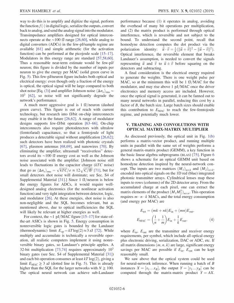
V. TRAINING AND CONVOLUTIONS WITHOPTICAL MATRIX-MATRIX MULTIPLIER
As discussed previously, the optical unit in Fig. 1(b)performs a matrix-vector product, and running multipleunits in parallel with the same set of weights performs ageneral matrix-matrix product (GEMM), a key function inthe basic linear algebra subprograms (BLAS) [75]. Figure 6shows a schematic for an optical GEMM unit based onhomodyne detection inspired by the neural-network con-cept. The inputs are two matrices ðM1Þm×k and ðM2Þn×k,encoded into optical signals on the 1D red (blue) integratedphotonic transmitter arrays. Cylindrical lenses map theseinputs to rows (columns) of the 2D detector array. From theaccumulated charge at each pixel, one can extract thematrix elements of the product ðM1MT
2 Þm×n. This operationrequires m · n · k MACs, and the total energy consumption(and energy per MAC) are
Etot ¼ ðmkþ nkÞEin þ ðmnÞEout;
EMAC ¼�1
nþ 1
m
�Ein þ
1
kEout; ð4Þ
where Ein, Eout are the transmitter and receiver energyrequirements, per symbol, which include all optical energyplus electronic driving, serialization, DAC or ADC, etc. Ifall matrix dimensions ðm; n; kÞ are large, significant energysavings per MAC are possible if Ein, Eout can be keptreasonably small.We saw above that the optical system could be used
for neural-network inference. When running a batch of Binstances X ¼ ½x1…xB�, the output Y ¼ ½y1…yB� can becomputed through the matrix-matrix product Y ¼ AX.
RYAN HAMERLY et al. PHYS. REV. X 9, 021032 (2019)
021032-6

In fully connected layers, training and backpropagationalso rely heavily on GEMM. The goal of training is to findthe set of weights AðkÞ that minimize the loss function L,which characterizes the inaccuracy of the model. Trainingtypically proceeds by gradient-based methods. Since theloss depends on the network output, we start at the finallayer and work backward, a process called backpropagation[7,8]. At each layer, we compute the gradient ð∇ALÞij ¼∂L=∂Aij from the quantity ð∇YLÞij ¼ ∂L=∂Yij, and propa-gate the derivative back to the input ð∇XLÞij ¼ ∂L=∂Xij
[Fig. 7(a)]. These derivatives are computed from the chainrule and can be written as matrix-matrix multiplications:
∇AL ¼ ð∇YLÞXT; ∇XL ¼ ATð∇YLÞ: ð5Þ
Once the derivative has been propagated to ∇XðkÞL (forlayer k), we use the chain rule to compute ∇Yðk−1ÞL ¼f0ð∇XðkÞLÞ and proceed to the previous layer. In this way,we sequentially compute the derivatives ∇AðkÞL at eachlayer in the neural network.In addition to fully connected layers, it is also possible
to run convolutional layers on the optical GEMM unit byemploying a “patching” technique [76]. In a convolutionallayer, the input xij;k is a W ×H image with C channels.This is convolved to produce an output yij;k of dimensionW0 ×H0 with C0 channels [13]:
yij;k ¼Xi0j0;l
Ki0j0;klxðsxiþi0Þðsyjþj0Þ;l: ð6Þ
Here Ki0j0;kl is the convolution kernel, a four-dimensionaltensor of size Kx × Ky × C0 × C, and ðsx; syÞ are the stridesof the convolution. Naively vectorizing Eq. (6) and runningit as a fully connected matrix-vector multiply is veryinefficient because the resulting matrix is sparse andcontains many redundant entries. Patching expresses theimage as a matrix X of size KxKyC ×W0H0, where eachcolumn corresponds to a vectorized Kx × Ky patch of theimage [Fig. 7(b)]. The elements of the kernel are rearrangedto form a (dense) matrix K of size C0 × KxKyC.Equation (6) can then be computed by taking the matrix-matrix product Y ¼ KX, which has size C0 ×W0H0. Onvirtually any microprocessor, GEMM is a highly optimizedfunction with very regular patterns of memory access; thebenefits of rewriting the convolution as a GEMM greatlyoutweigh the redundancy of data storage arising fromoverlapping patches [76]. The time required to rearrangethe image as a patch matrix is typically very smallcompared to the time to compute the GEMM [77] (andcan be further reduced if necessary with network-on-chiparchitectures [78] or optical buffering [79]); therefore, byaccelerating the GEMM, the optical matrix multiplierwill significantly improve the speed and energy efficiencyof convolutional layers. Note also that, since we areperforming the convolution as a matrix-matrix (rather than
(a)
(b)
II
FIG. 6. (a) Matrix multiplication with a 2D detector array,two 1D transmitter arrays, and optical fan-out. Imaging lenses(including cylindrical lenses for row and column fan-out) notshown. (b) Schematic diagram of transmitter array.
(a)
(b)
FIG. 7. Applications of optical GEMM. (a) Required matrixoperations for inference, training, and backpropagation in adeep neural network. (b) Patching technique to recast a con-volution (Kx ¼ Ky ¼ 3, sx ¼ sy ¼ 2 shown) as a matrix-matrixmultiplication.
LARGE-SCALE OPTICAL NEURAL NETWORKS BASED ON … PHYS. REV. X 9, 021032 (2019)
021032-7

matrix-vector) operation, it is possible to obtain energysavings even without running the neural network on largebatches of data. Computing the convolution requiresW0H0KxKyC0C MACs. Following Eq. (4), the energy perMAC (not including memory rearrangement for patching) is
EMAC ¼�1
C0 þ1
W0H0
�|fflfflfflfflfflfflfflfflfflffl{zfflfflfflfflfflfflfflfflfflffl}
1=cin
Ein þ1
KxKyC|fflfflffl{zfflfflffl}1=cout
Eout: ð7Þ
The coefficients cin¼ð1=Cþ1=W0H0Þ−1 and cout¼KxKyCgovern the energy efficiency when we are limited by input oroutput energies (transmitter or receiver and associatedelectronics). Since reading a 32-bit register takes ∼pJ ofenergy [13], a reasonable lower bound for near-term systemsis Ein, Eout ≳ pJ. Thus it is essential that cin, cout ≫ 1 forthe energy performance of the optical system to beat anASIC (∼pJ=MAC).As a benchmark problem, we consider ALEXNET [1], the
first convolutional neural network to perform competitivelyat the ImageNet Large-Scale Visual Recognition Challenge[9]. ALEXNET consists of five convolutional (CONV) layersand three fully connected (FC) layers, and consistent withdeep neural networks generally, the majority of the energyconsumption comes from the CONV layers [13]. Table Igives the layer dimensions and the values of cin, cout for theCONV layers in ALEXNET [1]. The MAC-weightedaverages for all layers are hcini > 100 and hcouti >1000. Thus, even under extremely conservative assump-tions of Ein, Eout ≳ 100 pJ (comparable to DRAM readenergies [13,14]), it is still possible to achieve sub-pJ/MACperformance.
More advanced technology, such as few-femtojouleoptical interconnects [26], may significantly reduce Einand Eout, and therefore the energy per MAC. However, theperformance is still fundamentally limited by detector shotnoise [see, e.g., Eq. (3) for FC layers]. Section S3 ofSupplemental Material [31] extends the shot-noise analysisto the case of matrix-matrix products needed for theconvolutional case. Using a pretrained ALEXNET model(see Sec. VII for details), Figure 8(b) shows the top-tenaccuracy on the ImageNet validation set as a function of thenumber of photons per MAC nMAC. Consistent with Fig. 3,there are two limits: nMAC ≪ 1 corresponds to the randomguess regime with 99% error rate (for top-ten accuracy with1000 classes), while nMAC ≫ 1 recovers the accuracy of thenoiseless model.The dashed lines in Fig. 8(b) show the fictitious case
where noise is present in only a single layer, while the solidgreen line corresponds to the case where all layers havenoise and nMAC is the same for each layer. Not all layerscontribute equally to the noise: CONV1 is the mostsensitive, requiring nMAC ≳ 20, while the deeper layers(particularly the fully connected layers) can tolerate much
TABLE I. Layers in ALEXNET [1]. Input dimension is227 × 227 × 3. Values of cin, cout are calculated from Eq. (7).Max pooling layers after CONV1, CONV2, and CONV5 are usedto reduce the image size, but the relative computational cost forthese layers is negligible.
Layer Output Kernel Stride MACs cin cout
CONV1 55 × 55 × 96 11 × 11 4 105M 93 363(Pool) 27 × 27 × 96 � � � 2 � � � � � � � � �CONV2 27 × 27 × 256 5 × 5 1 448M 189 2400(Pool) 13 × 13 × 256 � � � 2 � � � � � � � � �CONV3 13 × 13 × 384 3 × 3 1 150M 117 2304CONV4 13 × 13 × 384 3 × 3 1 224M 117 3456CONV5 13 × 13 × 256 3 × 3 1 150M 102 3456(Pool) 6 × 6 × 256 � � � 2 � � � � � � � � �FC1 4096 � � � � � � 38M � � � � � �FC2 4096 � � � � � � 17M � � � � � �FC3 1000 � � � � � � 4M � � � � � �
Total CONV layers 1.08G 132 1656Total FC layers 59M � � � � � �
M ¼ 106; G ¼ 109.
(b)
(a)
FIG. 8. (a) Schematic drawing of ALEXNET, which consists offive convolutional layers and 3 fully connected layers. Poolingand normalization steps not shown. (b) Error rate for pretrainedALEXNET as a function of nMAC. Dashed lines show the effectof noise in a single layer, while solid green line shows theperformance of the actual machine where all layers have noise.
RYAN HAMERLY et al. PHYS. REV. X 9, 021032 (2019)
021032-8
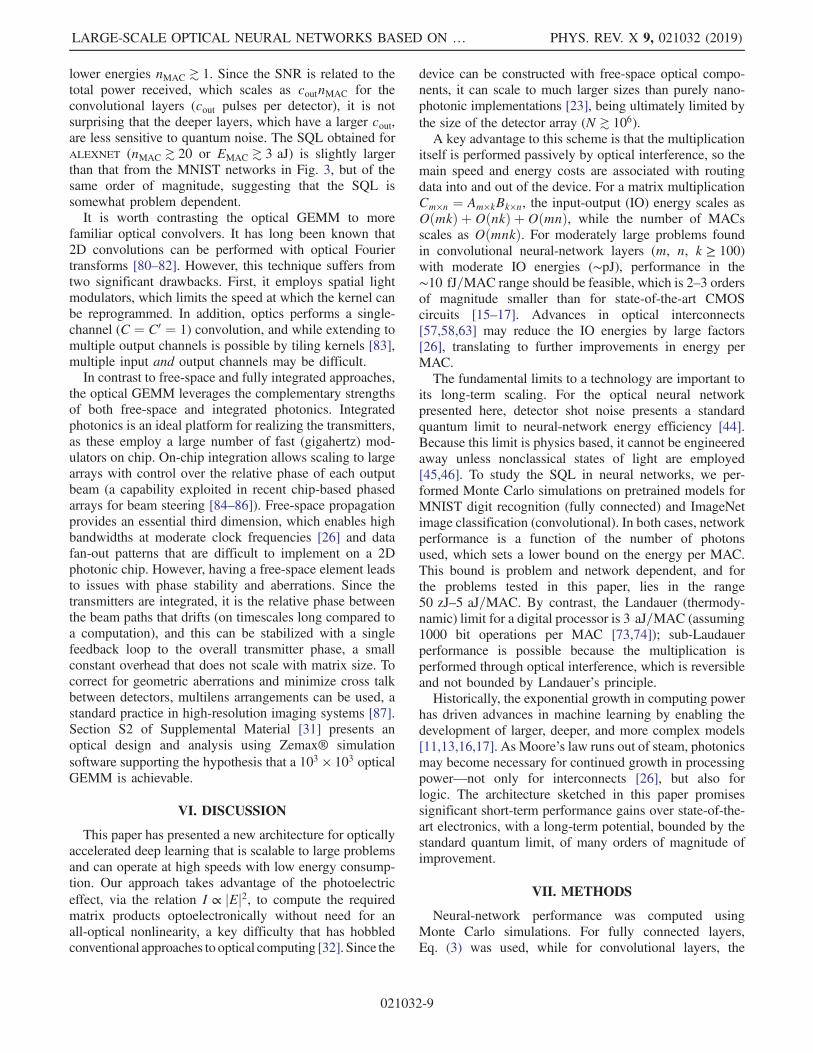
lower energies nMAC ≳ 1. Since the SNR is related to thetotal power received, which scales as coutnMAC for theconvolutional layers (cout pulses per detector), it is notsurprising that the deeper layers, which have a larger cout,are less sensitive to quantum noise. The SQL obtained forALEXNET (nMAC ≳ 20 or EMAC ≳ 3 aJ) is slightly largerthan that from the MNIST networks in Fig. 3, but of thesame order of magnitude, suggesting that the SQL issomewhat problem dependent.It is worth contrasting the optical GEMM to more
familiar optical convolvers. It has long been known that2D convolutions can be performed with optical Fouriertransforms [80–82]. However, this technique suffers fromtwo significant drawbacks. First, it employs spatial lightmodulators, which limits the speed at which the kernel canbe reprogrammed. In addition, optics performs a single-channel (C ¼ C0 ¼ 1) convolution, and while extending tomultiple output channels is possible by tiling kernels [83],multiple input and output channels may be difficult.In contrast to free-space and fully integrated approaches,
the optical GEMM leverages the complementary strengthsof both free-space and integrated photonics. Integratedphotonics is an ideal platform for realizing the transmitters,as these employ a large number of fast (gigahertz) mod-ulators on chip. On-chip integration allows scaling to largearrays with control over the relative phase of each outputbeam (a capability exploited in recent chip-based phasedarrays for beam steering [84–86]). Free-space propagationprovides an essential third dimension, which enables highbandwidths at moderate clock frequencies [26] and datafan-out patterns that are difficult to implement on a 2Dphotonic chip. However, having a free-space element leadsto issues with phase stability and aberrations. Since thetransmitters are integrated, it is the relative phase betweenthe beam paths that drifts (on timescales long compared toa computation), and this can be stabilized with a singlefeedback loop to the overall transmitter phase, a smallconstant overhead that does not scale with matrix size. Tocorrect for geometric aberrations and minimize cross talkbetween detectors, multilens arrangements can be used, astandard practice in high-resolution imaging systems [87].Section S2 of Supplemental Material [31] presents anoptical design and analysis using Zemax® simulationsoftware supporting the hypothesis that a 103 × 103 opticalGEMM is achievable.
VI. DISCUSSION
This paper has presented a new architecture for opticallyaccelerated deep learning that is scalable to large problemsand can operate at high speeds with low energy consump-tion. Our approach takes advantage of the photoelectriceffect, via the relation I ∝ jEj2, to compute the requiredmatrix products optoelectronically without need for anall-optical nonlinearity, a key difficulty that has hobbledconventional approaches to optical computing [32]. Since the
device can be constructed with free-space optical compo-nents, it can scale to much larger sizes than purely nano-photonic implementations [23], being ultimately limited bythe size of the detector array (N ≳ 106).A key advantage to this scheme is that the multiplication
itself is performed passively by optical interference, so themain speed and energy costs are associated with routingdata into and out of the device. For a matrix multiplicationCm×n ¼ Am×kBk×n, the input-output (IO) energy scales asOðmkÞ þOðnkÞ þOðmnÞ, while the number of MACsscales as OðmnkÞ. For moderately large problems foundin convolutional neural-network layers (m, n, k ≥ 100)with moderate IO energies (∼pJ), performance in the∼10 fJ=MAC range should be feasible, which is 2–3 ordersof magnitude smaller than for state-of-the-art CMOScircuits [15–17]. Advances in optical interconnects[57,58,63] may reduce the IO energies by large factors[26], translating to further improvements in energy perMAC.The fundamental limits to a technology are important to
its long-term scaling. For the optical neural networkpresented here, detector shot noise presents a standardquantum limit to neural-network energy efficiency [44].Because this limit is physics based, it cannot be engineeredaway unless nonclassical states of light are employed[45,46]. To study the SQL in neural networks, we per-formed Monte Carlo simulations on pretrained models forMNIST digit recognition (fully connected) and ImageNetimage classification (convolutional). In both cases, networkperformance is a function of the number of photonsused, which sets a lower bound on the energy per MAC.This bound is problem and network dependent, and forthe problems tested in this paper, lies in the range50 zJ–5 aJ=MAC. By contrast, the Landauer (thermody-namic) limit for a digital processor is 3 aJ=MAC (assuming1000 bit operations per MAC [73,74]); sub-Laudauerperformance is possible because the multiplication isperformed through optical interference, which is reversibleand not bounded by Landauer’s principle.Historically, the exponential growth in computing power
has driven advances in machine learning by enabling thedevelopment of larger, deeper, and more complex models[11,13,16,17]. As Moore’s law runs out of steam, photonicsmay become necessary for continued growth in processingpower—not only for interconnects [26], but also forlogic. The architecture sketched in this paper promisessignificant short-term performance gains over state-of-the-art electronics, with a long-term potential, bounded by thestandard quantum limit, of many orders of magnitude ofimprovement.
VII. METHODS
Neural-network performance was computed usingMonte Carlo simulations. For fully connected layers,Eq. (3) was used, while for convolutional layers, the
LARGE-SCALE OPTICAL NEURAL NETWORKS BASED ON … PHYS. REV. X 9, 021032 (2019)
021032-9

convolution was performed by first forming the patchmatrix [Fig. 7(b)] and performing the matrix-matrixmultiplication (noise model discussed in Sec. S3 ofSupplemental Material [31]). The weights for the fullyconnected MNIST neural networks were trained on a GPUusing TENSORFLOW. A pretrained TENSORFLOW version ofALEXNET (available online at Ref. [88]) was modified toimplement the quantum noise model and used forImageNet classification. Simulations were performed onan NVIDIA Tesla K40 GPU.
ACKNOWLEDGMENTS
R. H. is supported by an IC Postdoctoral ResearchFellowship at MIT, administered by ORISE throughU.S. DOE and Office of the Director of NationalIntelligence (ODNI). L. B. is supported by a DoctoralPostgraduate Scholarship from the Natural Sciences andEngineering Research Council of Canada (NSERC). D. E.and M. S. acknowledge support from the U.S. AROthrough the ISN at MIT (No. W911NF-18-2-0048). Theauthors acknowledge John Peurifoy (MIT) for training anumber of the MNIST neural-network models, andNVIDIA Corporation for the donation of the Tesla K40GPU used in this research. We are grateful to Joel Emer(NVIDIA and MIT) and Vivienne Sze (MIT) for helpfuldiscussions.
[1] A. Krizhevsky, I. Sutskever, and G. E. Hinton, ImageNetClassification with Deep Convolutional Neural Networks,in Advances in Neural Information Processing Systems(NeurIPS, Tahoe, Nevada, 2012), pp. 1097–1105.
[2] T. Young, D. Hazarika, S. Poria, and E. Cambria, RecentTrends in Deep Learning Based Natural Language Process-ing, IEEE Comput. Intell. Mag. 13, 55 (2018).
[3] D. Silver, T. Hubert, J. Schrittwieser, I. Antonoglou, M. Lai,A. Guez, M. Lanctot, L. Sifre, D. Kumaran, T. Graepelet al., A General Reinforcement Learning Algorithm thatMasters Chess, Shogi, and Go Through Self-Play, Science362, 1140 (2018).
[4] J. Gilmer, S. S. Schoenholz, P. F. Riley, O. Vinyals, andG. E. Dahl, Neural Message Passing for Quantum Chem-istry, in Proceedings of the 34th International Conferenceon Machine Learning (ICML) (ACM, Sydney, 2017),pp. 1263–1272.
[5] D. Wang, A. Khosla, R. Gargeya, H. Irshad, and A. H. Beck,Deep Learning for Identifying Metastatic Breast Cancer,arXiv:1606.05718.
[6] F. Rosenblatt, The Perceptron: A Probabilistic Model forInformation Storage and Organization in the Brain,Psychol. Rev. 65, 386 (1958).
[7] P. Werbos, Beyond Regression: New Tools for Predictionand Analysis in the Behavioral Sciences, Ph.D. thesis,Harvard University, 1974.
[8] Y. LeCun, L. Bottou, Y. Bengio, and P. Haffner, Gradient-Based Learning Applied to Document Recognition, Proc.IEEE 86, 2278 (1998).
[9] O. Russakovsky, J. Deng, H. Su, J. Krause, S. Satheesh, S.Ma, Z. Huang, A. Karpathy, A. Khosla, M. Bernstein, A. C.Berg, and L. Fei-Fei, ImageNet Large Scale Visual Rec-ognition Challenge, Int. J. Comput. Vis. 115, 211 (2015).
[10] G. E. Moore, Cramming More Components onto IntegratedCircuits, Electronics 38, 114 (1965).
[11] D. Steinkraus, I. Buck, and P. Y. Simard, Using GPUs forMachine Learning Algorithms, in Proceedings of the EighthInternational Conference on Document Analysis and Rec-ognition, 2005 (IEEE, New York, 2005), pp. 1115–1120,https://doi.org/10.1109/ICDAR.2005.251.
[12] A. Canziani, E. Culurciello, and A. Paszke, Evaluation ofNeural Network Architectures for Embedded Systems, inIEEE International Symposium on Circuits and Systems(ISCAS), 2017 (IEEE, New York, 2017), pp. 1–4, https://doi.org/10.1109/ISCAS.2017.8050276.
[13] V. Sze, Y.-H. Chen, T.-J. Yang, and J. S. Emer, EfficientProcessing of Deep Neural Networks: A Tutorial andSurvey, Proc. IEEE 105, 2295 (2017).
[14] M. Horowitz, Computing’s Energy Problem (and WhatWe Can Do About It), in IEEE International Solid-StateCircuits Conference (ISSCC), Digest of Technical Papers(IEEE, New York, 2014), pp. 10–14, https://doi.org/10.1109/ISSCC.2014.6757323.
[15] S.W. Keckler, W. J. Dally, B. Khailany, M. Garland, and D.Glasco, GPUs and the Future of Parallel Computing, IEEEMicro 31, 7 (2011).
[16] T. Chen, Z. Du, N. Sun, J. Wang, C. Wu, Y. Chen, and O.Temam, DianNao: A Small-Footprint High-ThroughputAccelerator for Ubiquitous Machine-Learning, ACM Sig-plan Not. 49, 269 (2014).
[17] N. P. Jouppi, C. Young, N. Patil, D. Patterson, G. Agrawal,R. Bajwa, S. Bates, S. Bhatia, N. Boden, A. Borchers et al.,In-Datacenter Performance Analysis of a Tensor Process-ing Unit, in Proceedings of the ACM/IEEE 44th AnnualInternational Symposium on Computer Architecture (ISCA),2017 (IEEE, New York, 2017), pp. 1–12, https://doi.org/10.1145/3079856.3080246.
[18] S. George, S. Kim, S. Shah, J. Hasler, M. Collins, F. Adil, R.Wunderlich, S. Nease, and S. Ramakrishnan, A Program-mable and Configurable Mixed-Mode FPAA SoC, IEEETransactions on Very Large Scale Integration (VLSI)Systems 24, 2253 (2016).
[19] K.-H. Kim, S. Gaba, D. Wheeler, J. M. Cruz-Albrecht, T.Hussain, N. Srinivasa, and W. Lu, A Functional HybridMemristor Crossbar-Array/CMOS System for Data Storageand Neuromorphic Applications, Nano Lett. 12, 389 (2012).
[20] C. Li, D. Belkin, Y. Li, P. Yan, M. Hu, N. Ge, H. Jiang, E.Montgomery, P. Lin, Z. Wang et al., Efficient and Self-Adaptive In-Situ Learning in Multilayer Memristor NeuralNetworks, Nat. Commun. 9, 2385 (2018).
[21] B. Feinberg, S. Wang, and E. Ipek, Making MemristiveNeural Network Accelerators Reliable, in Proceedings ofthe 2018 IEEE International Symposium on High Perfor-mance Computer Architecture (HPCA) (IEEE, New York,2018), pp. 52–65, https://doi.org/10.1109/HPCA.2018.00015.
RYAN HAMERLY et al. PHYS. REV. X 9, 021032 (2019)
021032-10

[22] X. Lin, Y. Rivenson, N. T. Yardimci, M. Veli, Y. Luo, M.Jarrahi, and A. Ozcan, All-Optical Machine Learning UsingDiffractive Deep Neural Networks, Science 361, 1004(2018).
[23] Y. Shen, N. C. Harris, S. Skirlo, M. Prabhu, T. Baehr-Jones,M. Hochberg, X. Sun, S. Zhao, H. Larochelle, D. Englundet al.,Deep Learning with Coherent Nanophotonic Circuits,Nat. Photonics 11, 441 (2017).
[24] A. N. Tait, T. F. Lima, E. Zhou, A. X. Wu, M. A. Nahmias,B. J. Shastri, and P. R. Prucnal, Neuromorphic PhotonicNetworks Using Silicon Photonic Weight Banks, Sci. Rep. 7,7430 (2017).
[25] J. M. Kahn and D. A. B. Miller, Communications ExpandsIts Space, Nat. Photonics 11, 5 (2017).
[26] D. A. B. Miller, Attojoule Optoelectronics for Low-EnergyInformation Processing and Communications, J. LightwaveTechnol. 35, 346 (2017).
[27] A. Rogalski, Progress in Focal Plane Array Technologies,Prog. Quantum Electron. 36, 342 (2012).
[28] A. Marandi, Z. Wang, K. Takata, R. L. Byer, and Y.Yamamoto, Network of Time-Multiplexed Optical Para-metric Oscillators as a Coherent Ising Machine, Nat.Photonics 8, 937 (2014).
[29] T. Inagaki, K. Inaba, R. Hamerly, K. Inoue, Y. Yamamoto,and H. Takesue, Large-Scale Ising Spin Network Based onDegenerate Optical Parametric Oscillators, Nat. Photonics10, 415 (2016).
[30] P. L. McMahon, A. Marandi, Y. Haribara, R. Hamerly,C. Langrock, S. Tamate, T. Inagaki, H. Takesue, S.Utsunomiya, K. Aihara et al., A Fully Programmable100-Spin Coherent Ising Machine with All-to-All Connec-tions, Science 354, 614 (2016).
[31] See Supplemental Material at http://link.aps.org/supplemental/10.1103/PhysRevX.9.021032 for homodyneproduct implementation details, aberration analysis, anddetailed derivations of shot noise, Johnson noise, andLandauer limit formulas.
[32] D. A. B. Miller, Are Optical Transistors the Logical NextStep?, Nat. Photonics 4, 3 (2010).
[33] A. N. Tait, M. A. Nahmias, B. J. Shastri, and P. R. Prucnal,Broadcast and Weight: An Integrated Network for ScalablePhotonic Spike Processing, J. Lightwave Technol. 32, 4029(2014).
[34] K. Vandoorne, W. Dierckx, B. Schrauwen, D. Verstraeten,R. Baets, P. Bienstman, and J. Van Campenhout, TowardOptical Signal Processing Using Photonic Reservoir Com-puting, Opt. Express 16, 11182 (2008).
[35] Y. Paquot, F. Duport, A. Smerieri, J. Dambre, B. Schrauwen,M. Haelterman, and S. Massar, Optoelectronic ReservoirComputing, Sci. Rep. 2, 287 (2012).
[36] L. Larger, M. C. Soriano, D. Brunner, L. Appeltant, J. M.Gutierrez, L. Pesquera, C. R. Mirasso, and I. Fischer,Photonic Information Processing Beyond Turing: An Opto-electronic Implementation of Reservoir Computing, Opt. E20, 3241 (2012).
[37] M. A. Nahmias, B. J. Shastri, A. N. Tait, and P. R. Prucnal,A Leaky Integrate-and-Fire Laser Neuron for UltrafastCognitive Computing, IEEE J. Sel. Topics Quantum Elec-tron. 19, 1 (2013).
[38] D. Brunner, S. Reitzenstein, and I. Fischer, All-OpticalNeuromorphic Computing in Optical Networks of Semi-conductor Lasers, in Proceedings of the 2016 IEEEInternational Conference on Rebooting Computing (ICRC)(IEEE, New York, 2016), pp. 1–2, https://doi.org/10.1109/ICRC.2016.7738705.
[39] M. Reck, A. Zeilinger, H. J. Bernstein, and P. Bertani,Experimental Realization of Any Discrete Unitary Oper-ator, Phys. Rev. Lett. 73, 58 (1994).
[40] W. R. Clements, P. C. Humphreys, B. J. Metcalf, W. S.Kolthammer, and I. A. Walmsley, Optimal Design forUniversal Multiport Interferometers, Optica 3, 1460 (2016).
[41] A. Einstein, Über Einen die Erzeugung und Verwandlungdes Lichtes Betreffenden Heuristischen Gesichtspunkt,Ann. Phys. (Berlin) 322, 132 (1905).
[42] D. F. Walls and G. J. Milburn, Quantum Optics (SpringerScience & Business Media, Berlin, 2007).
[43] M.M. Hayat, B. E. A. Saleh, and J. A. Gubner, Shot-Noise-Limited Performance of Optical Neural Networks, IEEETrans. Neural Networks 7, 700 (1996).
[44] C. M. Caves, Quantum-Mechanical Noise in an Interfer-ometer, Phys. Rev. D 23, 1693 (1981).
[45] M. T. Jaekel and S. Reynaud, Quantum Limits in Interfero-metric Measurements, Europhys. Lett. 13, 301 (1990).
[46] H. Grote, K. Danzmann, K. L. Dooley, R. Schnabel, J.Slutsky, and H. Vahlbruch, First Long-Term Application ofSqueezed States of Light in a Gravitational-Wave Observa-tory, Phys. Rev. Lett. 110, 181101 (2013).
[47] L. Holmstrom and P. Koistinen, Using Additive Noise inBack-Propagation Training, IEEE Trans. Neural Networks3, 24 (1992).
[48] G. E. Hinton, N. Srivastava, A. Krizhevsky, I. Sutskever, andR. R. Salakhutdinov, Improving Neural Networks by Prevent-ing Co-Adaptation of Feature Detectors, arXiv:1207.0580.
[49] H. Gibbs, Optical Bistability: Controlling Light with Light(Elsevier, New York, 2012).
[50] C. M. Savage and H. J. Carmichael, Single Atom OpticalBistability, IEEE J. Quantum Electron. 24, 1495 (1988).
[51] C. Santori, J. S. Pelc, R. G. Beausoleil, N. Tezak, R.Hamerly, and H. Mabuchi, Quantum Noise in Large-ScaleCoherent Nonlinear Photonic Circuits, Phys. Rev. Applied1, 054005 (2014).
[52] J. Kerckhoff, M. A. Armen, and H. Mabuchi, Remnantsof Semiclassical Bistability in the Few-Photon Regime ofCavity QED, Opt. Express 19, 24468 (2011).
[53] X. Ji, F. A. S. Barbosa, S. P. Roberts, A. Dutt, J. Cardenas,Y. Okawachi, A. Bryant, A. L. Gaeta, and M. Lipson, Ultra-Low-Loss On-Chip Resonators with Sub-Milliwatt Para-metric Oscillation Threshold, Optica 4, 619 (2017).
[54] S. Hu, M. Khater, R. Salas-Montiel, E. Kratschmer, S.Engelmann, W.M. J. Green, and S. M. Weiss, ExperimentalRealization of Deep-Subwavelength Confinement in Dielec-tric Optical Resonators, Sci. Adv. 4, eaat2355 (2018).
[55] C. Wang, C. Langrock, A. Marandi, M. Jankowski, M.Zhang, B. Desiatov, M.M. Fejer, and M. Loncar, Ultrahigh-Efficiency Second-Harmonic Generation in NanophotonicPPLN Waveguides, Optica 5, 1438 (2018).
[56] D. A. B. Miller, Energy Consumption in Optical Modulatorsfor Interconnects, Opt. Express 20, A293 (2012).
LARGE-SCALE OPTICAL NEURAL NETWORKS BASED ON … PHYS. REV. X 9, 021032 (2019)
021032-11

[57] C. Sun, M. T. Wade, Y. Lee, J. S. Orcutt, L. Alloatti, M. S.Georgas, A. S. Waterman, J. M. Shainline, R. R. Avizienis,S. Lin et al., Single-Chip Microprocessor that Communi-cates Directly Using Light, Nature (London) 528, 534(2015).
[58] A. H. Atabaki, S. Moazeni, F. Pavanello, H. Gevorgyan, J.Notaros, L. Alloatti, M. T. Wade, C. Sun, S. A. Kruger, H.Meng et al., Integrating Photonics with Silicon Nanoelec-tronics for the Next Generation of Systems on a Chip,Nature (London) 556, 349 (2018).
[59] A. Michaels and E. Yablonovitch, Inverse Design of NearUnity Efficiency Perfectly Vertical Grating Couplers, Opt.Express 26, 4766 (2018).
[60] S. Saeedi, S. Menezo, G. Pares, and A. Emami, A 25 Gb=s3D-Integrated CMOS/Silicon-Photonic Receiver for Low-Power High-Sensitivity Optical Communication, J. Light-wave Technol. 34, 2924 (2016).
[61] B. E. Jonsson, An Empirical Approach to Finding EnergyEfficient ADC Architectures, in Proceedings of 2011International Workshop on ADC Modeling, Testing andData Converter Analysis and Design (IMEKO, Orvieto,Italy, 2011), pp. 1–6, https://www.imeko.org/publications/iwadc-2011/IMEKO-IWADC-2011-28.pdf.
[62] M. Notomi, K. Nozaki, A. Shinya, S. Matsuo, and E.Kuramochi, Toward fJ/Bit Optical Communication in aChip, Opt. Commun. 314, 3 (2014).
[63] E. Timurdogan, C.M. Sorace-Agaskar, J. Sun, E. S. Hosseini,A. Biberman, and M. R. Watts, An Ultralow Power AthermalSilicon Modulator, Nat. Commun. 5, 4008 (2014).
[64] C. Koos, J. Leuthold, W. Freude, M. Kohl, L. Dalton, W.Bogaerts, A. L. Giesecke, M. Lauermann, A. Melikyan,S. Koeber et al., Silicon-Organic Hybrid (SOH) andPlasmonic-Organic Hybrid (POH) Integration, J. Light-wave Technol. 34, 256 (2016).
[65] C. Haffner, D. Chelladurai, Y. Fedoryshyn, A. Josten, B.Baeuerle, W. Heni, T. Watanabe, T. Cui, B. Cheng, S. Sahaet al., Low-Loss Plasmon-Assisted Electro-optic Modulator,Nature (London) 556, 483 (2018).
[66] S. A. Srinivasan, M. Pantouvaki, S. Gupta, H. T. Chen, P.Verheyen, G. Lepage, G. Roelkens, K. Saraswat, D. VanThourhout, P. Absil et al., 56 Gb=s Germanium WaveguideElectro-Absorption Modulator, J. Lightwave Technol. 34,419 (2016).
[67] K. Nozaki, S. Matsuo, T. Fujii, K. Takeda, M. Ono, A.Shakoor, E. Kuramochi, and M. Notomi, Photonic-CrystalNano-Photodetector with Ultrasmall Capacitance for On-Chip Light-to-Voltage Conversion without an Amplifier,Optica 3, 483 (2016).
[68] T. Ishi, J. Fujikata, K. Makita, T. Baba, and K. Ohashi, SiNano-Photodiode with a Surface Plasmon Antenna, Jpn. J.Appl. Phys. 44, L364 (2005).
[69] L. Tang, S. E. Kocabas, S. Latif, A. K. Okyay, D.-S. Ly-Gagnon, K. C. Saraswat, and D. A. B. Miller, Nanometre-Scale Germanium Photodetector Enhanced by a Near-Infrared Dipole Antenna, Nat. Photonics 2, 226 (2008).
[70] L. Cao, J.-S. Park, P. Fan, B. Clemens, and M. L.Brongersma, Resonant Germanium Nanoantenna Photo-detectors, Nano Lett. 10, 1229 (2010).
[71] J. R. Pierce, Physical Sources of Noise, Proc. IRE 44, 601(1956).
[72] R. Landauer, Irreversibility and Heat Generation in theComputing Process, IBM J. Res. Dev. 5, 183 (1961).
[73] M. Nagamatsu, S. Tanaka, J. Mori, T. Noguchi, and K.Hatanaka, A 15-ns 32 × 32-Bit CMOS Multiplier with anImproved Parallel Structure, IEEE J. Solid State Circuits25, 494 (1990).
[74] H. H. Yao and E. E. Swartzlander, Serial-Parallel Multi-pliers, in Proceedings of the Twenty-Seventh AsilomarConference on Signals, Systems and Computers, 1993(IEEE, New York, 1993), pp. 359–363, https://doi.org/10.1109/ACSSC.1993.342534.
[75] C. L. Lawson, R. J. Hanson, D. R. Kincaid, and F. T. Krogh,Basic Linear Algebra Subprograms for FORTRAN Usage,ACM Trans. Math. Softw. 5, 308 (1979).
[76] S. Chetlur, C. Woolley, P. Vandermersch, J. Cohen, J. Tran,B. Catanzaro, and E. Shelhamer, cuDNN: Efficient Prim-itives for Deep Learning, arXiv:1410.0759.
[77] X. Li, G. Zhang, H. H. Huang, Z. Wang, and W. Zheng,Performance Analysis of GPU-Based Convolutional NeuralNetworks, in Proceedings of the 45th InternationalConference on Parallel Processing (ICPP), 2016 (IEEE,New York, 2016), pp. 67–76, https://doi.org/10.1109/ICPP.2016.15.
[78] Y.-H. Chen, T. Krishna, J. S. Emer, and V. Sze, Eyeriss: AnEnergy-Efficient Reconfigurable Accelerator for Deep Con-volutional Neural Networks, IEEE J. Solid-State Circuits52, 127 (2017).
[79] H. Bagherian, S. Skirlo, Y. Shen, H. Meng, V. Ceperic,and M. Soljacic, On-Chip Optical Convolutional NeuralNetworks, arXiv:1808.03303.
[80] A. V. Lugt, Signal Detection by Complex Spatial Filtering,IEEE Trans. Inf. Theory 10, 139 (1964).
[81] E. G. Paek and D. Psaltis, Optical Associative MemoryUsing Fourier Transform Holograms, Opt. Eng. 26, 265428(1987).
[82] N. J. New, Reconfigurable Optical Processing System,U.S. Patent No. 9,594,394 (2017).
[83] J. Chang, V. Sitzmann, X. Dun, W. Heidrich, and G.Wetzstein, Hybrid Optical-Electronic Convolutional NeuralNetworks with Optimized Diffractive Optics for ImageClassification, Sci. Rep. 8, 12324 (2018).
[84] J. Sun, E. Timurdogan, A. Yaacobi, E. S. Hosseini, andM. R. Watts, Large-Scale Nanophotonic Phased Array,Nature (London) 493, 195 (2013).
[85] S. W. Chung, H. Abediasl, and H. Hashemi, A Monolithi-cally Integrated Large-Scale Optical Phased Array inSilicon-on-Insulator CMOS, IEEE J. Solid-State Circuits53, 275 (2018).
[86] C. T. Phare, M. C. Shin, S. A. Miller, B. Stern, and M.Lipson, Silicon Optical Phased Array with High-EfficiencyBeam Formation over 180 Degree Field of View, arXiv:1802.04624.
[87] W. J. Smith, Modern Optical Engineering (Tata McGraw-Hill Education, New York, 1966).
[88] Y. Peng, Implementation of ALEXNET with Tensorflow, https://github.com/ykpengba/AlexNet-A-Practical-Implementation.
RYAN HAMERLY et al. PHYS. REV. X 9, 021032 (2019)
021032-12