
Large area CMOS photosensors for time-resolved measurements · Acknowledgements “And once the...
168
Large area CMOS photosensors for time-resolved measurements Vor der Fakultät für Ingenieurwissenschaften, Abteilung Elektrotechnik und Informationstechnik der Universität Duisburg-Essen zur Erlangung des akademischen Grades Doktor der Ingenieurwissenschaften genehmigte Dissertation von Elena Poklonskaya aus Sewastopol Gutachter: (Prof. Dr. Holger Vogt) Gutachter: (Prof. Dr. Jürgen Oehm) Tag der mündlichen Prüfung: (20.07.2015)
Transcript of Large area CMOS photosensors for time-resolved measurements · Acknowledgements “And once the...

Large area CMOS photosensors for
time-resolved measurements
Vor der Fakultät für Ingenieurwissenschaften,
Abteilung Elektrotechnik und Informationstechnik
der Universität Duisburg-Essen
zur Erlangung des akademischen Grades
Doktor der Ingenieurwissenschaften
genehmigte Dissertation
von
Elena Poklonskaya
aus
Sewastopol
Gutachter: (Prof. Dr. Holger Vogt)
Gutachter: (Prof. Dr. Jürgen Oehm)
Tag der mündlichen Prüfung: (20.07.2015)

Acknowledgements
“And once the storm is over, you won’t
remember how you made it through, how
you managed to survive. You won’t even be
sure, whether the storm is really over. But
one thing is certain. When you come out of
the storm, you won’t be the same person
who walked in. That’s what this storm’s all
about.” - Haruki Murakami.
My PhD work became such a storm for me, tough to go through, sometimes gloomy,
discouraging, the storm which from time to time let you feel lost and sad, hopeless. But this
storm has taught me how to fight my way through and how to be strong, how to believe in
myself and in the work I am doing, how to be true to myself and my goals and never ever stop
half way. I would not be where I am now if I would not choose this road.
I also do realize that I would not accomplish it alone, without continuous support from my
professors, my supervisor, colleagues, family and friends. They were always there by my side
and have never let me to lose my way.
I would like to thank my professor Prof. Holger Vogt for supporting and encouraging me, for
being such a great role model for me. Thanks to my supervisor Dr. Daniel Durini for always
finding the right way to motivate me. I have to also thank Prof. Anton Grabmaier for regularly
criticizing my work and thus pushing me to progress and develop me as a scientist, and of
course I am deeply grateful to Fraunhofer Institute of Microelectronic Circuits and Systems
(Fraunhofer IMS) and the Spectro Ametek company for financial support.
I thank my colleagues Melanie Jung, Christian Schmitz, Ulfig Wiebke, Stefan Bröcker,
Adrian Driewer, David Arutinov, Olaf Schrey and Claudia Busch for the endless help and
support along the way, for cheering me up and enlightening me in numerous friendly
conversations.

A lot of thanks goes to my students Yan Cheng, Florian Caspers, Kai Fischer, Song Jian,
Alexander Schmitz, whom I have supervised, and who helped me a lot with the simulations and
experiments.
I am grateful to my family: my brother Alexey Poklonskiy, for being a role model for me, my
father Alexander Poklonskiy for always believing in me and being proud of me no matter what,
and my mother Larisa Poklonskaya for never letting me alone with all that difficulties I had,
for being not just my mother, but my closest friend.

Abstract
Many industrial applications require linear photosensors, which exhibit high sensitivity and low
noise. The atomic emission spectroscopy is one of such applications. This spectroscopic method
delivers the information about the qualitative and quantitative composition of an analyte.
Since 1960 photomultiplier tubes (PMT) were used as standard detectors in the field of
spectrometry due to their high speed of response and low dark current. Recently, solid-state line
sensors have established themselves as a promising alternative to the photomultiplier tubes.
Newly used in hybrid emission spectrometers, CCD line sensors are able to detect the part of
the spectra in the ultra-violet (for wavelengths longer than some 250 nm), visible, and near
infra-red ranges sent to them by a narrow bandwidth optical grid. However, CCD technology
does not have the ability of random pixel addressing, non-destructive readout and time-resolved
measurements, which causes the necessity of reading out the complete sensor several times to
adjust the necessary charge collection period required to be able to distinguish between
neighbouring lines in the spectrograph. This consumes a lot of measuring time and also adds
additional reset noise and diminishes the signal-to-noise ratio after each readout.
A CMOS approach can be a good alternative to CCD. Developed and optimized in this thesis,
a lateral drift-field photodetector (LDPD) based CMOS line sensor offers the possibility for the
so called time-gating together with the feature of non-destructive readout and charge
accumulation over several cycles without the need for the reset phase.
Large photoactive areas of up to 1 mm as well as fast charge transfer and low dark currents are
all dominant requirements for the sensors used in optical emission spectroscopy. These are the
main goals that should be achievable with the structures proposed in this thesis.
Pixel charge transfer from the photoactive area into the sense node is examined in detail in this
work. Different mechanisms of the charge transport are studied. Dark current in the LDPD pixel
is analysed on using varied pixel structures. A novel pixel design to enhance the charge transfer
efficiency is presented.
Different pixel types are proposed and thoroughly characterized. Finally, the best pixel structure
is used to fabricate a prototype line sensor, the operating characteristics of which are also
examined in detail.

i
Table of contents Acknowledgements .................................................................................................................. 2
Abstract.....................................................................................................................................5
Table of contents ....................................................................................................................... i
List of figures .......................................................................................................................... vi
List of tables ............................................................................................................................ xi
1 Introduction ...................................................................................................... 13
1.1 Motivation and Work Content .................................................................................... 13
1.2 Optical Atomic Emission Spectroscopy ..................................................................... 14
1.2.1 History ......................................................................................................................................14
1.2.2 Theoretical Foundation .............................................................................................................15
1.2.3 The Electromagnetic Spectrum ................................................................................................16
1.2.4 Excitation in Plasma .................................................................................................................16
1.2.5 Spark AES ................................................................................................................................17
1.2.6 Inductively Coupled Plasma (ICP) AES...................................................................................17
1.3 Detectors used in Spark (or ICP) AES ....................................................................... 17
1.3.1. Photomultiplier Tubes (PMT) ..........................................................................................................19
1.3.2. CCD ..................................................................................................................................................20
1.3.3 CMOS Line Sensor Alternative .........................................................................................................21
1.4 Comparison of Technologies Used in AES ................................................................ 21
1.5 State of the Art Detectors used in AES ...................................................................... 22
1.6 Improvements Proposed and Studied by Author ........................................................ 25
2 Variants of the CMOS-based Photodetector Types for AES Application .. 26
2.1 Photodetectors based on a Standard PN Junction ...................................................... 26
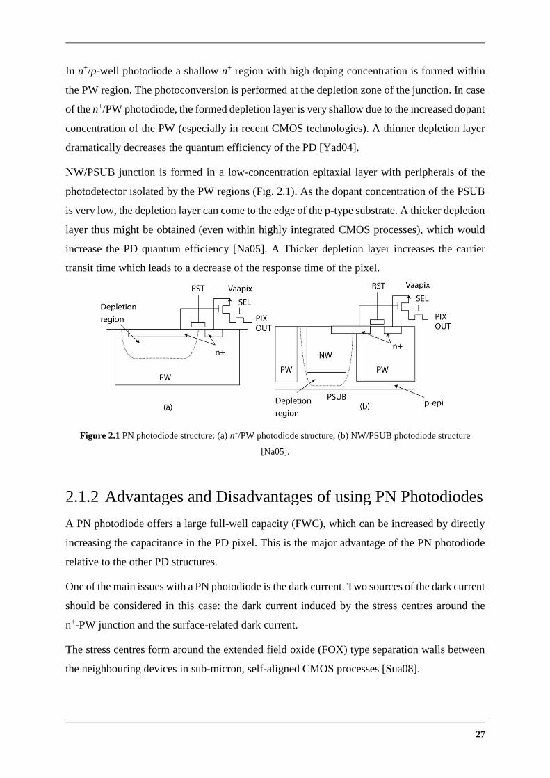
2.1.1 PN Photodiode Structure ..........................................................................................................26
2.1.2 Advantages and Disadvantages of using PN Photodiodes ........................................................27
2.2 Pinned Photodiode (PPD) ........................................................................................... 29
2.2.1 PPD Structure ...........................................................................................................................29
2.2.2 Advantages and Disadvantages of PPD Photodiodes ...............................................................30

ii
2.3 Different Possibilities for Enhancing Charge Transfer in PD .................................... 31
2.3.1 The Adjustment Shape of the Photodetector .....................................................................................31
2.3.2. P-epitaxial Layer with the Doping Gradient .....................................................................................33
2.3.3. Multiple N-doped Implantations ......................................................................................................33
2.4 Introducing Lateral Drift-Field PD (LDPD) .............................................................. 34
2.4.1 LDPD Structure .................................................................................................................................35
2.4.2 Advantages and Disadvantages of LDPD .........................................................................................36
3 LDPD based Pixel Concept for TRM AES .................................................... 37
3.1 LDPD Pixel ................................................................................................................ 37
3.2 Readout Principle ....................................................................................................... 39
3.3 Charge Transfer Mechanism in LDPD ....................................................................... 41
3.4 Function of the LDPD in AES ................................................................................... 42
3.5 Pixel Readout and Control Circuit ............................................................................. 43
3.6 Detector Design: Challenges and Proposed Solutions ............................................... 44
4 Characteristics of the LDPD pixel .................................................................. 46
4.1 Performance Characteristics ....................................................................................... 46
4.1.1 Spectral Responsivity and Quatum Efficiency .........................................................................47
4.1.2 Conversion Gain .......................................................................................................................48
4.1.3 Full Well Capacity (Saturation Capacity) .................................................................................49
4.1.4 SNR and Dynamic Range .........................................................................................................49
4.1.5 Linearity ...................................................................................................................................49
4.1.6 Noise Sources in LDPD ............................................................................................................50
4.1.6.1 Fixed Pattern Noise............................................................................................................. 50
4.1.6.2 Temporal Noise .................................................................................................................. 50
4.2 Dark Current ............................................................................................................... 53
4.2.1 Depletion Dark Current ............................................................................................................53
4.2.2 Diffusion (Bulk) Dark Current .................................................................................................57
4.2.3 Surface Dark Current ................................................................................................................59
4.2.4 Dark Current in the LDPD Pixel ..............................................................................................60
4.3 Charge transfer ........................................................................................................... 63
4.3.1 Thermal Diffusion of the Charge Carriers ................................................................................63
4.3.2 Self-induced Drift Field ............................................................................................................65
4.3.3 Fringing Field ...........................................................................................................................66
4.3.4 Lateral Drift-field .....................................................................................................................67

iii
4.3.5 Charge Transfer Mechanisms in the LDPD Pixel ....................................................................68
4.4 Potential Profile within the n-well.............................................................................. 70
4.5 TG and DG Operation ................................................................................................ 73
4.6 Crosstalk ..................................................................................................................... 74
4.6.1 Electrical Crosstalk ...................................................................................................................74
4.6.2 Optical Crosstalk ......................................................................................................................75
4.6.3 Crosstalk between LDPD Pixels...............................................................................................76
5 Development of the LDPD-Based Pixel .......................................................... 79
5.1 Goal specification ....................................................................................................... 79
5.2 Pixel design ................................................................................................................ 80
5.2.1 Photodiode Test Structures .......................................................................................................80
5.2.1.1 Quantum Efficiency Measurements .................................................................................... 81
5.2.1.2 I/V Characteristics .............................................................................................................. 83
5.3 Electrical parameters .................................................................................................. 87
5.3.1 Output Voltage Swing ..............................................................................................................87
5.3.2 Floating Diffusion Capacitance ................................................................................................88
5.3.3 Spectral Responsivity ...............................................................................................................89
5.3.4 Noise and Dynamic Range .......................................................................................................89
5.4 Pixel Test Structures................................................................................................... 90
5.5 Measurements of the Performance ............................................................................. 91
5.5.1 Responsivity and Quantum Efficiency .....................................................................................92
5.5.2 Dark Current .............................................................................................................................97
5.5.3 Transfer Time ...........................................................................................................................99
5.5.4 LDPD Test Pixel Optimization...............................................................................................102
6 Experimental results ...................................................................................... 104
6.1 Basic Characterization using the Photon-Transfer Method (PTM) ............... 104
6.1.1 Test Structures and Measurement Details ..............................................................................105
6.1.2 Spectral Responsivity and Quantum Efficiency .....................................................................106
6.1.2.1 "Wide" n-well ................................................................................................................... 106
6.1.2.2 Overlap of the n-well with TG .......................................................................................... 107
6.1.2.3 P-well between the Gates ................................................................................................. 108
6.1.2.4 CG with Different Length ................................................................................................. 109
6.1.2.5 TG with Different Length ................................................................................................. 109
6.1.2.6 Conclusions ...................................................................................................................... 110
6.1.3 Sense Node Capacitance, DR, Saturation Capacitance ..........................................................110
iv
6.1.4 PRNU, DRNU ........................................................................................................................110
6.2 Dark Current Characterization ................................................................................. 111
6.2.1 The Test Structure and Measurement Methodology ...............................................................111
6.2.2 Dark Current versus CG Geometry ........................................................................................112
6.2.3 Dark Current versus TG Geometry.........................................................................................113
6.2.4 P-well between the Gates .......................................................................................................114
6.2.5 Dark Current Temperature Dependence .................................................................................115
6.2.6 Conclusions ............................................................................................................................116
6.3 Charge Transfer ........................................................................................................ 117
6.3.7 The Test Structure and Measurement Methodology ...............................................................117
6.3.8 Transfer Time Dependency on Gradient in the n-well ...........................................................118
6.3.9 Transfer Time Dependency on the Number of the Impinging Photons ..................................119
6.3.10 Transfer Time Dependency on TG and CG length .................................................................121
6.3.11 Transfer Time from Different Parts of PA .............................................................................123
6.3.12 Conclusions ............................................................................................................................124
6.4 Pixel Transfer Time Optimization ............................................................................ 124
6.5 Charge Transfer Improvement ................................................................................. 125
6.5.1 Mask Generation and Pixel Layout ........................................................................................125
6.5.2 Simulation of the Doping Concentration Profile ....................................................................128
6.5.3 Simulation of the Electrostatic Potential Profile.....................................................................129
6.5.4 Simulation of the Charge Transfer .........................................................................................131
6.5.5 Conclusions ............................................................................................................................134
6.6 Crosstalk ................................................................................................................... 134
6.6.1 Test Structure and Measurement Methodology ......................................................................134
6.6.2 Electrical Crosstalk Characterization .....................................................................................136
6.6.3 Optical Crosstalk Characterization .........................................................................................140
6.6.4 Conclusions ............................................................................................................................142
7 CMOS Line Sensor with 1 x 368 Pixels ........................................................ 143
7.1 Circuit and Sensor Design ........................................................................................ 143
7.2 Pixel Characteristics ................................................................................................. 145
7.3 Measurements .......................................................................................................... 146
8 Summary ......................................................................................................... 149
8.1 Future work .............................................................................................................. 150
Abbreviations ....................................................................................................................... 155

v
Bibliography ........................................................................................................................ 157

vi
List of figures Figure 1.1 Spectrum obtained from gold ore [AP]. .......................................................................... 15
Figure 1.2 Energy diagram of electron (energy absorption and emission) [Ob]. .......................... 16
Figure 1.3 Part of the electromagnetic spectrum, that contains the spectral lines of most of the
elements commonly detected via optical emission spectroscopy [Ob]. .................................. 16
Figure 1.4 Time-dependent radiation emission diagram typically obtained during an AES
measurement [Ob]. ..................................................................................................................... 18
Figure 1.5 Schematic view of the PMT [Bos97]. ............................................................................... 19
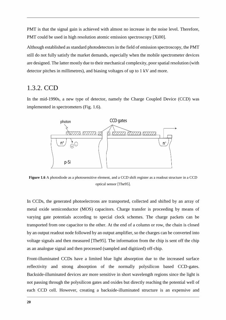
Figure 1.6 A photodiode as a photosensitive element, and a CCD shift register as a readout
structure in a CCD optical sensor [The95]. .............................................................................. 20
Figure 1.7 Concept of DOM pixel [Li12]. .......................................................................................... 24
Figure 1.8 Concept of the pixel proposed by Yoon [Yo09]. ............................................................. 25
Figure 2.1 PN photodiode structure: (a) n+/PW photodiode structure, (b) NW/PSUB photodiode
structure [Na05]. ......................................................................................................................... 27
Figure 2.2 PN photodiode pixel structure [Oh08]. ........................................................................... 28
Figure 2.3 Pinned photodiode pixel structure [Na05]. ..................................................................... 29
Figure 2.4 Behaviour of photo-generated carriers in PPD [Oh08]. ................................................ 30
Figure 2.5 (a) Trapezoidal shape photodiode, (b) potential profile of rectangular photodiode (c)
trapezoidal photodiode [Sh10]. .................................................................................................. 32
Figure 2.6 Cross-section of the PD proposed by Tubert [Tu09]. .................................................... 33
Figure 2.7 Cross sectional view of three n-type photodetector implant (a) graded potential
profile (b) operation of the PD [Jar01]. .................................................................................... 34
Figure 2.8 Schematic representation of the LDPD [Dur10]. ........................................................... 35
Figure 3.1 Cross-sectional schematic view of the LDPD [Po13]. ..................................................... 38
Figure 3.2 Readout principle for FD and DD [Du13]. ..................................................................... 39
Figure 3.3 N-well PD voltage evolution vs time in darkness [Mae03]............................................. 40
Figure 3.4 Charge transfer in LDPD, integration phase [Ch13]. .................................................... 41
Figure 3.5 Charge transfer in LDPD, readout phase [Ch13]. ......................................................... 42
Figure 3.6 Schematic representation of various controlling, input and output signals used during
the operation of the LDPD-based pixel in spark-induced emission spectroscopy
applications. ................................................................................................................................. 43
Figure 3.7 Schematic circuit diagram of the pixel readout and control circuit [Dur13]. ............. 44
Figure 4.1 Cross section of the LDPD pixel with demonstrating of the dark current mechanism.
...................................................................................................................................................... 53
Figure 4.2 Carrier generation and recombination process via a trap level in the band gap. ...... 54
Figure 4.3 Cross section of the LDPD pixel (photoactive area). ...................................................... 60

vii
Figure 4.4 Cross section of the LDPD pixel (TG and CG region). ................................................. 61
Figure 4.5 Cross section of the LDPD pixel (FD region). ................................................................. 62
Figure 4.6 Cross section of the LDPD pixel and the demonstration of the dark current
mechanism (in control electrodes area). ................................................................................... 63
Figure 4.7 Schematic illustration of the surface potential a) without and b) with fringing fields
[The95]. ........................................................................................................................................ 67
Figure 4.8 Charge transfer mechanisms in the LDPD pixel. ........................................................... 68
Figure 4.9 Charge flow underneath the control gates (VCG =1.75[V], VTG=2[V]). ......................... 69
Figure 4.10 Fringing field at the Si-SiO2 interface a) at a shallow depth b) deeper c) in the silicon
bulk [The95]. ............................................................................................................................... 69
Figure 4.11 Electrostatic potential underneath the control gates (VCG =1.75 V, VTG=2 V); small
length control electrodes (LCG= 2.86 µm LTG= 2.3 µm). ........................................................... 70
Figure 4.12 Electrostatic potential underneath the control gates (VCG =1.75 V, VTG=2 V); large
length control electrodes (LCG= 10 µm LTG= 3.7 µm). .............................................................. 70
Figure 4.13 Simulated electrostatic potential profile of the LDPD pixel fabricated with high and
low implant dose; CG is biased at 1.8 V and TG at 2 V, FD at 2.3 V. .................................... 71
Figure 4.14 Fermi level for the Si as a function of temperature and impurity concentration
[Sz07]. ........................................................................................................................................... 72
Figure 4.15 Simulated electron flow in the LDPD pixel test structure with small overlap of the n-
well over TG (a) charge transfer phase (b) draining phase. ................................................... 73
Figure 4.16 Simulated electron flow in the LDPD pixel test structure with larger overlap of the
n-well over TG (a) charge transfer phase (b) draining phase. ................................................ 73
Figure 4.17 Simulated electrostatic potential in the LDPD pixel with the smaller length of TG
and applied 0V; the cut was made at the potential maximum depth. .................................... 74
Figure 4.18 Schematic view of the electrical crosstalk. .................................................................... 75
Figure 4.19 Schematic view of the optical crosstalk. ........................................................................ 76
Figure 4.20 2D TCAD simulation of the n-well of the two neighbouring LDPD pixels. ............... 77
Figure 4.21 (a) 2D TCAD simulation of the one pixel electrostatic potential between TG and DG,
the potential on the n-well under the TG is 0V and under the DG 2.5 V, (b) electrostatic
potential under the TG and DG for two different depths (y). ................................................ 78
Figure 4.22 (a) 2D TCAD simulation of the electrostatic potential between CGs of neighbouring
pixels, the potential on the n-well under both CGs is 2.2 𝐕, (b) electrostatic potential under
the CGs for one fixed depth -12.7µm. .................................................................... 78
Figure 5.1 LDPD photodiode test structure. ..................................................................................... 81
Figure 5.2 Quantum efficiency vs wavelength curves obtained from the LDPD test structures
using three different passivation layers. ................................................................................... 82
viii
Figure 5.3 Quantum efficiency vs wavelength curves obtained from the LDPD test structures
with two different dose of the n-well implant. .......................................................................... 83
Figure 5.4 LDPD test structures used to measure total dark current. ........................................... 84
Figure 5.5 Dark current on LDPD test structures vs the dose of the implant n-well. ................... 86
Figure 5.6 Area and perimeter-dependent components of the dark current generated in the PDs
extracted from the measurements of the test structures. ........................................................ 87
Figure 5.7 Readout concept of the proposed LDPD pixel. ............................................................... 88
Figure 5.8 Layout used for the LDPD test pixel structures (5 pixels). ............................................ 90
Figure 5.9 Doping concentration profile of the LDPD n-well. ......................................................... 93
Figure 5.10 Doping concentration profile of the redesigned LDPD n-well. ................................... 94
Figure 5.11 Layout of the initial and redesigned LDPD n-well. ...................................................... 94
Figure 5.12 Doping concentration profile of the two neighbouring pixel n-wells. ......................... 95
Figure 5.13 Doping concentration profile of the LDPD pixel with low dose of n-well implant
(TG/FD area). .............................................................................................................................. 96
Figure 5.14 Doping concentration profile of the LDPD pixel with (a) and without (b) p-well
between TG/DG. ......................................................................................................................... 96
Figure 5.15 Total dark signal measured on LDPD test structures vs the length of the TG. ......... 98
Figure 5.16 Total dark signal measured on LDPD test structures vs the dose of the implant n-
well. .............................................................................................................................................. 99
Figure 5.17 New 5-pixel test structure with two "dummy" pixels located on both sides of the test
cluster. .......................................................................................................................................... 99
Figure 5.18 Pixel timing diagram employed to characterize the transfer time. .......................... 100
Figure 5.19 Transfer time definition. ............................................................................................... 101
Figure 6.1 Output characteristics of the pixel test structures with different overlaps of the n-well
with TG. ..................................................................................................................................... 107
Figure 6.2 Dark signal of the LDPD test structures with different length of the CG.................. 113
Figure 6.3 Dark signal of the LDPD test structures with different geometries of the n-well. .... 115
Figure 6.4 Dark signal of the LDPD test pixel vs reverse temperature. ....................................... 116
Figure 6.5 Transfer time measurements for the pixels with different implantation doses of the n-
well. Illumination power 714.2 W/m2. ..................................................................................... 119
Figure 6.6 Transfer time measurements under the different illumination power. ...................... 120
Figure 6.7 Transfer time measurements under the different illumination power. ...................... 121
Figure 6.8 Transfer time measurements for the pixels with different CG lengths. Illumination
power 342 W/m2. ....................................................................................................................... 122
Figure 6.9 Transfer time measurements for the pixels with different TG and CG lengths.
Illumination power 159.2 W/m2. .............................................................................................. 122

ix
Figure 6.10 Transfer time measurements for the pixels with different CG lengths.
Illumination power 342 W/m2. ................................................................................................. 123
Figure 6.11 New pixel configuration layout and n-well fabrication steps. ................................... 126
Figure 6.12 Implantation steps forming newly designed n-well. ................................................... 126
Figure 6.13 Proposed pixel design and electrostatic potential diagram of the pixel. .................. 128
Figure 6.14 Simulated doping concentration profile of the proposed design. .............................. 129
Figure 6.15 Simulated potential profile of the proposed design. ................................................... 130
Figure 6.16 Electrostatic potential profile of the proposed pixel design. ..................................... 131
Figure 6.17 (a) Technology cross-section of the simulated pixel structure showing the window
selected for illumination; (b) timing diagram used for different pixel controlling signals. 132
Figure 6.18 Transient simulation results show the change of the carrier concentration density in
the photoactive area of the original LDPD and the proposed pixel. .................................... 133
Figure 6.19 Transient simulations of the proposed pixel design with different implants
concentrations. .......................................................................................................................... 133
Figure 6.20 Schematic cross-section of one pixel block. ................................................................. 135
Figure 6.21 Schematic view of the test pixel block. The pixel in the middle is either (a) fully
uncovered or (b-d) partially uncovered. The dashed area marks the uncovered region. .. 135
Figure 6.22 Measurement setup for electrical crosstalk characterization. .................................. 137
Figure 6.23 Wavelength dependent electrical crosstalk for LDPD pixel test-structures with lower
implantation dose (test chip A), and slightly higher implantation dose (test chip C). ........ 138
Figure 6.24 Pixel crosstalk test results. Pixel 0 is active, pixels ±1, ±2 are optically black. ........ 138
Figure 6.25 Output characteristics of the block (d) from Figure 6.19 (a) test pixel A (b) test pixel
C. ................................................................................................................................................ 139
Figure 6.26 Measurement setup used to evaluate electrical crosstalk. ......................................... 141
Figure 6.27 Schematic representation of the (a) impinging radiation striking the pixel
photoactive area under angles of 30° or 10°; (b) impinging radiation striking the pixel
photoactive area under angles of -30° or -10°. ....................................................................... 142
Figure 6.28 Crosstalk versus the incident angle of collimated light for the test chip E. ............ 142
Figure 7.1 CMOS line sensor with 1 x 368 pixels. ......................................................................... 143
Figure 7.2 Simplified diagram of the test chip (including readout path and buffer biasing). .... 144
Figure 7.3 Circuit diagram of the LDPD-based pixel used for the line sensor development. .... 145
Figure 7.4 Bonded test chip photo.................................................................................................... 146
Figure A1 Measurement setup. ........................................................................................................ 151
Figure A2 Illumination source. ........................................................................................................ 151
Figure B1 Measured dark signla of the pixel (1x368 CMOS line sensor). ... Fehler! Textmarke nicht
definiert.

x
Figure C1 Example of the PMT curve of the pixel (1x368 CMOS line sensor) .... Fehler! Textmarke
nicht definiert.
Figure C2 Output signla of the pixel in dependence on light intensity (1x368 CMOS line sensor)
.................................................................................................... Fehler! Textmarke nicht definiert.

xi
List of tables Table 1.1 Summary of the main advantages and disadvantages of PMT, CCD and CMOS........ 22
Table 1.2 State of the art detectors used in AES............................................................................... 23
Table 5.1 Goal specification. ............................................................................................................... 79
Table 5.2 PD test structures. ............................................................................................................... 85
Table 5.3 Calculated dark current. .................................................................................................... 85
Table 5.4 Characteristics of the test pixels. ....................................................................................... 91
Table 5.5 Characterized test structures splits. .................................................................................. 91
Table 5.6 Measurement results of the test pixel structures. ............................................................ 92
Table 5.7 Dark current measured for the LDPD test structures with different dose of the n-well
implant. ........................................................................................................................................ 97
Table 5.8 Transfer time measured for the LDPD test structures with different dose of the n-well
implant. ...................................................................................................................................... 101
Table 5.9 Measurement results of the LDPD test structures. ........................................................ 102
Table 6.1 Characteristics of the test pixels. ..................................................................................... 105
Table 6.2 Calculated spectral responsivity and quantum efficiency of the test pixel structures
with "narrow"/"wide" n-well .................................................................................................. 106
Table 6.3 Calculated spectral responsivity and quantum efficiency of the test pixel structures
with different overlaps of n-well with TG. ............................................................................. 108
Table 6.4 Calculated spectral responsivity and quantum efficiency of the test pixel structures
with and without p-well between TG and DG. .................................................................... 108
Table 6.5 Calculated spectral responsivity and quantum efficiency of the test pixel structures
with different lengths of CG. ................................................................................................... 109
Table 6.6 Calculated spectral responsivity and quantum efficiency of the test pixel structures
with different length of CG. ..................................................................................................... 109
Table 6.7 Varied characteristics of the test chips. .......................................................................... 112
Table 6.8 Calculated dark current of the LDPD test structures with different lengths of CG. . 112
Table 6.9 Calculated dark current of the LDPD test structures with different length of TG. ... 114
Table 6.10 Calculated dark current of the LDPD test structures with the different lengths of the
PA. .............................................................................................................................................. 114
Table 6.11 Calculated dark current of the LDPD test structures with/without p-well between the
TG and DG. ............................................................................................................................... 115
Table 6.12 Varied characteristics of the test chips. ........................................................................ 117
Table 6.13 Pixel timing diagram employed to characterize the transfer time. ............................ 118
Table 6.14 Characterized pixel test structures. .............................................................................. 124
Table 6.15 Test chip parameters. ..................................................................................................... 136

xii
Table 7.1. Pixel parameters. ............................................................................................................ 145
Table 7.2. Test chips description. .................................................................................................... 146
Table 7.3 Measurement results of the 1 x 368 CMOS line sensor (Test chip D). ......................... 148

13
1 Introduction
The concept of the so called Lateral Drift-Field Photodector (LDPD) was proposed in [Du10],
and fabricated in a 0.35 µm CMOS technology. LDPD found its application in high-speed
detection, such as time-of-flight (ToF) based ranging and three dimensional (3D) imaging
[Sp11] [Dur11] [Sus13], where the specially designed n-well of the photodiode (PD), present
in each pixel, enables high charge transfer speeds and low image lag.
In a wide variety of applications, for example plasma induced optical emission or fluorescence
spectroscopy, high pixel sensitivities and high frame-rates are very important. The pixel
photosensitivity can be normally boosted by increasing photoactive area (PA). This might mean
having better fill-factors or increasing the pixel area all together. If the used pixel structures are
based on separated photoactive and pixel sense-node (SN) regions, as it is the case in the so
called Pinned Photodiode (PPD) based pixels [Gu97] [Yon03] [In03], it causes an important
increase of the charge transfer time from the photoactive area into the SN, where it must be
collected in order to be read out.
Using the LDPD concept in a CMOS line sensor solves some of these problems. It allows not
only for fast charge transfer in pixels with large PA, but also for a non-destructive readout
(NDR), and even time-resolved measurements as it will be explained below. This means that if
LDPD based pixels are used in a line-sensor, time-resolved measurements (TRM) become
possible, which dramatically decreases the time required for each experiment, and drastically
improves the quality of the measurement results for example, in optical atomic emission
spectroscopy applications.
1.1 Motivation and Work Content
The main goal of this work was to develop a CMOS line sensor using rectangular pixels with
large PA (10 µm × 200 µm), separated photoactive and sense-node regions and a fast charge
transfer between them, that delivers low noise, low dark current, and additionally enables the
feature of NDR, time-gating, as well as individual independent pixel access. Optimized for
optical atomic emission spectroscopy (OES or AES) applications, proposed LDPD based
CMOS line sensor should bring the innovations into the mentioned field and completely modify
the experimental flow.

14
Chapter 1 of this thesis relates a brief history of the AES physical background and application
requirements, then proceeds with bench marking of different state-of-the-art technologies.
Chapter 2 describes the different photodiode structures fabricated in the 0.35 µm CMOS
process chosen for this development. Chapter 3 discusses LDPD based proposed pixel
structures to be implemented in the CMOS line sensor. Chapter 4 provides the theoretical
analysis of all relevant features of these structures. Chapter 5 is dedicated to the LDPD pixel
development. In Chapter 6 full characterization of the LDPD pixel is given. Chapter 7 describes
the 1× 368 pixels CMOS line sensor that was developed as a demonstration of the proposed
technology, and Chapter 8 concludes the work with a summary and outlook.
1.2 Optical Atomic Emission Spectroscopy
AES is used in various industrial fields to analyse materials and substances. It includes several
analytic chemical techniques focused on elemental analysis, identification, quantification and
(sometimes) specification of the elemental makeup of the sample.
1.2.1 History
The first observation of atomic emission dates back to at least the first campfire where humans
observed a yellow colour in the flame. This colouring was caused by the relaxation of the
electron from the 3p to the 3s orbital in sodium (Na), and in part by carbone ions [Ju13]. Over
2000 years ago, colourful fireworks were developed in China. They employed the same (at that
time still unexplained) principle.
A few later discoveries drove continuous developments in the field of AES. Some of those are
certainly the first observation of the splitting of the white light into different colours if projected
on a glass prism, made by Newton in 1740; the development of diffraction gratings by Joseph
von Fraunhofer at the beginning of 19th century, who was able to separate white light into a
great variety of individual colours in a controlled manner; the discovery and explanation in
1859 by Kirchhoff and Bunsen of the first law of emission which states that “each body absorbs
the same radiation type that it emits when energised”; followed by the first quantitate analysis
of the sodium atoms using flame emission, performed by Champion, Pellet and Grenier in 1873;
or the fabrication of a concave grating by Rowland in 1882. Nevertheless, the real history of
the spectrometry began with the first patent of atomic absorption spectrometry granted to Walsh

15
in 1955, almost a century later. The first atomic absorption instrument became commercially
available in 1962 [Ju13].
1.2.2 Theoretical Foundation
In AES electrons of free atoms are temporarily excited to higher-energy states. By falling back,
they emit photons of specific wavelengths. The characteristic emission wavelength of each
particular element represents in a plot of emitted intensity vs. wavelength, so called spectral
line (see Fig. 1.1).
The wavelength and the intensity of the emitted radiation give the information about the type
of atoms (material) present in a sample under test and its quantity (Fig. 1.1).
Figure 1.1 Spectrum obtained from gold ore [AP].
The cause of atomic spectra can be explained by Bohr model and orbital theory [Ob]. According
to them an atom could be described as a positively charged nucleus that is surrounded by shells
(orbitals) populated negatively charged electrons. The further away from the nucleus the
electron orbital is, the higher is the electron energy level.
By transferring thermal or electrical energy (via for example flame or spark) to an electron, it
can be forced to migrate to an outer orbital corresponding to the higher energy level. This
process is transient, and after a short time, the electron “falls” back from the higher energy level
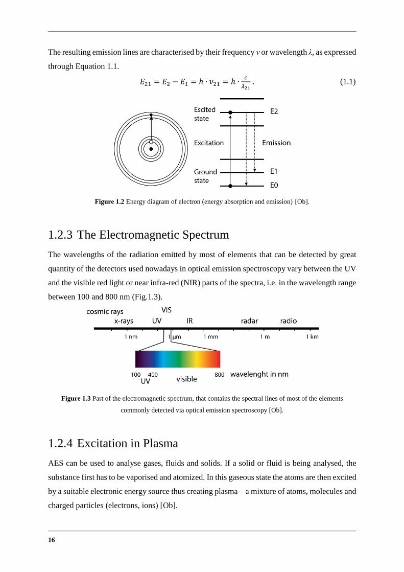
to the lower one, emitting the excess energy in a form of light. The diagram in Figure 1.2 shows
an electron excitation from the ground state E0 to the state with the energy E2, and the
subsequent return back to the state with the energy E1 or E0.
16
The resulting emission lines are characterised by their frequency ν or wavelength λ, as expressed
through Equation 1.1.
𝐸21 = 𝐸2 − 𝐸1 = ℎ ∙ 𝜈21 = ℎ ∙𝑐
𝜆21 . (1.1)
Figure 1.2 Energy diagram of electron (energy absorption and emission) [Ob].
1.2.3 The Electromagnetic Spectrum
The wavelengths of the radiation emitted by most of elements that can be detected by great
quantity of the detectors used nowadays in optical emission spectroscopy vary between the UV
and the visible red light or near infra-red (NIR) parts of the spectra, i.e. in the wavelength range
between 100 and 800 nm (Fig.1.3).
Figure 1.3 Part of the electromagnetic spectrum, that contains the spectral lines of most of the elements
commonly detected via optical emission spectroscopy [Ob].
1.2.4 Excitation in Plasma
AES can be used to analyse gases, fluids and solids. If a solid or fluid is being analysed, the
substance first has to be vaporised and atomized. In this gaseous state the atoms are then excited
by a suitable electronic energy source thus creating plasma – a mixture of atoms, molecules and
charged particles (electrons, ions) [Ob].
17
There are various methods used to produce plasma. One of the oldest methods is a plasma
excitation through ignition. However, most other elements require higher energy levels that can,
for instance, be supplied in the form of gas discharges.
These can be on several forms:
- stationary discharges (arc, glow-discharge, hollow cathode lamp),
- non-stationary discharges (spark, corona discharge, laser),
- time-dependent current/voltage sources (inductively coupled plasma).
In the current thesis, one particular type of spectroscopy was considered as a possible
application: spark AES or inductively coupled plasma AES.
1.2.5 Spark AES
An electrically generated spark in an argon atmosphere can be used to excite a large number of
elements. Plasma temperatures of over 10 000 K could be reached. The resulting spectra are
called “spark spectra” and display numerous atomic and ionic lines.
1.2.6 Inductively Coupled Plasma (ICP) AES
Radiofrequency (RF) discharge serves as an excitation source in ICP AES. At a core the ICP
has a temperature about 10 000 K. The atomic emission emanating from the plasma contains
information of about the origin of the element and its concentration in the sample.
1.3 Detectors used in Spark (or ICP) AES
For the experiments, that produce low light signals, the PD should have low noise and low dark
current, hence high dynamic range (DR) and signal-to-noise ratio (SNR).
To detect radiation spectra of all elements of interest, the detector should be sensitive in the UV
as well as in the visible range and have a large pixel area to satisfy the requirement of high
responsivity.
Different chemical compounds have different reflectance values, hence they radiate light with
different wavelengths. Practically, this means that specific elements could reflect so strongly
that the irradiated pixel is almost immediately saturated, while other elements reflect so weakly

18
that the signal is not strong enough to be detected at all. Defining a single charge integration
window for both cases can be extremely difficult. Therefore, monitoring the output signals of
every single pixel individually is essential, as well as an ability to define the starting point and
the length of the photocurrent integration window.
In spark emission spectroscopy applications, numeric atomic and ionic lines are excited and
emitted during the spark plasma discharge. However, only a certain number of these lines
contains information about the desired element. The resulting spectrum will also contain
interfering lines or a high level of continuous background radiation (BG). Typically, the
emission of ionic undesirable lines occurs during the sample excitation period, i.e. previous to
the emission of actual atomic lines (see Fig. 1.4).
Figure 1.4 Time-dependent radiation emission diagram typically obtained during an AES measurement [Ob].
Thus, with the help of time-resolved spectroscopy measurements many atomic lines can be
efficiently detected by eliminating the spurious background radiation during the measurement
[Ju13]. This method involves defining the right time window for the collection of the
photogenerated charges belonging to each emission channel (gate integration). Non-destructive
readout, random pixel access and charge separation in time (TRM) are thus becoming very
important features the used pixels should possess.
Summarizing all the points discussed above, the ideal detector implemented in an AES
application should satisfy the following requirements:
fast speed of response (on µs range)
low dark current ( ̴ 80 pA/cm2)

19
high sensitivity in UV/ VIS
high DR (̴ 50 dB)
random pixel access
gate integration (TRM)
non-destructive readout
During the past few years, photomultiplier tubes (PMT) and charge-coupled devices (CCD)
have been extensively used in AES [Yot03].
1.3.1. Photomultiplier Tubes (PMT)
Since 1960 photomultiplier tubes (PMT) have been standard detectors in the front field of spark
(ICP) AES due to their high speed of response, low dark current, and very high sensitivity, i.e.
internal charge multiplication factors.
PMT is a vacuum tube that contains in front a photosensitive material. This material is formed
into a photocathode, where impinging photons scatter electrons, exciting them enough to leave
the photocathode material (if energy of the photon is higher than the work function of the
photocathode material). These electrons are then accelerated in vacuum towards the first
dynode. Up to 5 electrons for every one impinging electron could be ejected by the first dynode.
This process repeats at each dynode inducing a multiplication effect. The electrons are finally
collected by the anode as it can be observed in Figure 1.5.
Figure 1.5 Schematic view of the PMT [Bos97].
The signal gain caused by the electron multiplication in the PMT depends on the voltage drop
established between the cathode and the anode (Fig. 1.5). One of the main advantages of the
20
PMT is that the signal gain is achieved with almost no increase in the noise level. Therefore,
PMT could be used in high resolution atomic emission spectroscopy [Xi00].
Although established as standard photodetectors in the field of emission spectroscopy, the PMT
still do not fully satisfy the market demands, especially when the mobile spectrometer devices
are designed. The latter mostly due to their mechanical complexity, poor spatial resolution (with
detector pitches in millimetres), and biasing voltages of up to 1 kV and more.
1.3.2. CCD
In the mid-1990s, a new type of detector, namely the Charge Coupled Device (CCD) was
implemented in spectrometers (Fig. 1.6).
Figure 1.6 A photodiode as a photosensitive element, and a CCD shift register as a readout structure in a CCD
optical sensor [The95].
In CCDs, the generated photoelectrons are transported, collected and shifted by an array of
metal oxide semiconductor (MOS) capacitors. Charge transfer is proceeding by means of
varying gate potentials according to special clock schemes. The charge packets can be
transported from one capacitor to the other. At the end of a column or row, the chain is closed
by an output readout node followed by an output amplifier, so the charges can be converted into
voltage signals and then measured [The95]. The information from the chip is sent off the chip
as an analogue signal and then processed (sampled and digitized) off-chip.
Front-illuminated CCDs have a limited blue light absorption due to the increased surface
reflectivity and strong absorption of the normally polysilicon based CCD-gates.
Backside-illuminated devices are more sensitive in short wavelength regions since the light is
not passing through the polysilicon gates and oxides but directly reaching the potential well of
each CCD cell. However, creating a backside-illuminated structure is an expensive and

21
time-consuming process. It requires thinning the substrates down to 50 µm or even 10 µm,
which involves complicated manufacturing processes used to avoid undesirable side-effects
[Yo03].
Although widely used in hybrid emission spectrometers, mostly due to the ability of
simultaneous multi-element inspection and high sensitivity, the CCDs cannot be read out in a
non-destructive manner and do not have random pixel access, which are some of the major
disadvantages of this kind of solid-state detectors [Ju13].
TRM possibility is thus also missing, as the whole CCD sensor has to be read out many times
during the experiment to determine the right time window for the measurements and exclude
the spurious background radiation, making each measurement time-consuming and impractical.
In this case, a complementary metal-oxide semiconductor (CMOS) approach can be a good
alternative to the CCDs.
1.3.3 CMOS Line Sensor Alternative
CMOS image sensors are mixed-signal circuits containing pixels, analogue signal processors,
analogue-to-digital converters, bias generators, timing generators, digital logic and memory
[Bi06]. The main advantages of CMOS imagers are [Wo97] [The01]:
o low power consumption
o on chip functionality and compatibility with standard CMOS technology
o random pixel access
o selective read-out mechanism.
The feature of non-destructive readout (possibility for signal monitoring, i.e. charge
accumulation over several integration periods) and the ability to perform time-resolved
measurements (collected charge separation in time), as well as lower manufacturing costs make
the CMOS image sensors an ideal alternative to CCDs in atomic emission spectroscopy
application.
1.4 Comparison of Technologies Used in AES
PMT-based optical emission spectrometer systems employ a single element detector for each
wavelength and are physically larger compared with CCDs. To achieve the same resolution
22
CCD sensor offers, many PMTs required to be positioned such that they can be illuminated
under a proper angle.
The very mature CCD technology yields high sensitivity, low dark currents, and high-quality
charge transport, but lacks the ability of time-resolved measurements and pixel output
monitoring. By using CCD, multiple integrations are required to receive the information from
the weaker lines of the spectrum and to subtract the highly intensive background emission lines.
CMOS image sensors were further developed over the last years, reaching the very similar
performance to the one normally expected only from CCD sensors in which the dark current
and noise are concerned. They have additionally an ability of random pixel access (selective
readout) and non-destructive readout with the possibility of time-resolved measurements.
On-pixel functionality is what also makes CMOS sensors superb alternative to CCD.
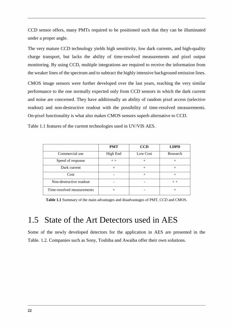
Table 1.1 features of the current technologies used in UV/VIS AES.
PMT CCD LDPD
Commercial use High End Low Cost Research
Speed of response + + + +
Dark current + + +
Cost - + +
Non-destructive readout - - + +
Time-resolved measurements + - +
Table 1.1 Summary of the main advantages and disadvantages of PMT, CCD and CMOS.
1.5 State of the Art Detectors used in AES
Some of the newly developed detectors for the application in AES are presented in the
Table. 1.2. Companies such as Sony, Toshiba and Awaiba offer their own solutions.
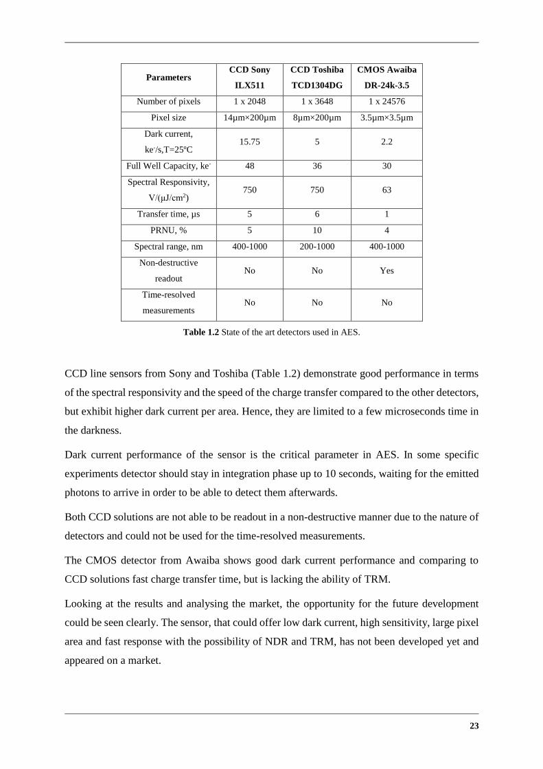
23
Parameters CCD Sony
ILX511
CCD Toshiba
TCD1304DG
CMOS Awaiba
DR-24k-3.5
Number of pixels 1 x 2048 1 x 3648 1 x 24576
Pixel size 14µm×200µm 8µm×200µm 3.5µm×3.5µm
Dark current,
ke-/s,T=25ºC 15.75 5 2.2
Full Well Capacity, ke- 48 36 30
Spectral Responsivity,
V/(μJ/cm2) 750 750 63
Transfer time, µs 5 6 1
PRNU, % 5 10 4
Spectral range, nm 400-1000 200-1000 400-1000
Non-destructive
readout No No Yes
Time-resolved
measurements No No No
Table 1.2 State of the art detectors used in AES.
CCD line sensors from Sony and Toshiba (Table 1.2) demonstrate good performance in terms
of the spectral responsivity and the speed of the charge transfer compared to the other detectors,
but exhibit higher dark current per area. Hence, they are limited to a few microseconds time in
the darkness.
Dark current performance of the sensor is the critical parameter in AES. In some specific
experiments detector should stay in integration phase up to 10 seconds, waiting for the emitted
photons to arrive in order to be able to detect them afterwards.
Both CCD solutions are not able to be readout in a non-destructive manner due to the nature of
detectors and could not be used for the time-resolved measurements.
The CMOS detector from Awaiba shows good dark current performance and comparing to
CCD solutions fast charge transfer time, but is lacking the ability of TRM.
Looking at the results and analysing the market, the opportunity for the future development
could be seen clearly. The sensor, that could offer low dark current, high sensitivity, large pixel
area and fast response with the possibility of NDR and TRM, has not been developed yet and
appeared on a market.

24
Many scientific groups are working on developing CMOS sensor that would enable time-gated,
time-resolved spectroscopy with effective background light elimination.
In draining-only modulation (DOM) CMOS pixel structure, proposed by Zhuo Li [Li12], the
time gating is done by draining the charges with only the draining gate (TD). Required signal
is detected in the following way: during the light pulse excitation, TD gate is opened to drain
unwanted charges generated by the excitation light. Closing the TD and opening the transfer
gate (TX), signal integration time begins.
A charge draining gate is located beside the carrier channel from the PPD (pinned photodiode)
to the readout node (Fig. 1.7); such design implies that the channel near TD should be very
accurately engineered to avoid potential barrier and ensure blocking of the charge carriers
during the accumulation phase.
Figure 1.7 Concept of DOM pixel [Li12].
Similar concept of time-gating was introduced by Yoon [Yo09] using three gates structure. The
draining gate and the transfer gate are attached on the two side of the PPD (pinned photodiode)
(Fig. 1.8).
Pixel structure proposed by Yoon could not be implemented in the pixel with a large
photoactive area; grated potential profile within the photoactive area is not applicable in such a
system, whereas a constant potential profile might cause an image lag in a pixel.

25
Figure 1.8 Concept of the pixel proposed by Yoon [Yo09].
1.6 Improvements Proposed and Studied by
Author
The proposed LDPD line sensor design uses a pixel with a large photoactive area, which assures
high responsivity. Specially designed UV transparent passivation provides sufficient optical
sensitivity in the ultraviolet spectrum. Based on LDPD CMOS line sensor enables fast charge
transfer and allows time-resolved measurements. Charge separation in time carried out via a
specially developed gate structure (multiple shutter system). Non-destructive read out is
allowing signal monitoring and charge accumulation over several cycles without need of the
reset phase. Photoactive area of the pixel is optimized to avoid image lag to occur by introducing
intrinsic drift field in the n-well and buried control electrodes design. Dark current is minimized
by incorporating "pinned" photodiode structure. Crosstalk is decreased by implementing
additional deep p-wells between neighbouring pixels.
The novel pixel design is proposed to increase charge transfer efficiency. The simulation results
shows decrease of the charge transfer time by about 16%.
26
2 Variants of the CMOS-based Photodetector
Types for AES Application
A pixel in a CMOS image sensor normally consists of the photodiode (or photodetector) part
and the correspondent readout circuit. Many variations of the pixels were proposed and
developed, incorporating several different photodiode structures.
All CMOS based photodetector types are based on the well-known photoelectric effect. For
almost fifty years p-n (or p-n-p) junctions were used to convert photons into electronic signals.
When light reaches a junction diode, electron-hole pairs are generated everywhere, when this
happens inside the depletion region, negatively charged electrons are separated from positively
charged holes by the electrical field induced across the junction. If generated outside of the
space-charge (or depletion) region (SCR), the photogenerated electrons must diffuse into the
SCR to be drifted and separated from the positively charged holes. Captured photogenerated
carriers are then normally collected over a certain charge collection (or photocurrent
integration) time, until they can be read out as a photocurrent or photovoltage signal.
2.1 Photodetectors based on a Standard PN
Junction
PN junction pixels represent the earliest generation of the pixel structures used in
semiconductor-based solid-state imaging. They can be easily incorporated into standard CMOS
processes with relatively minor modifications, which can be represented in a circuit schematic,
thus enabling image sensor design within general-purpose IC design environment [Na05]. This
makes PN pixels a cost-effective solution for the low-cost applications.
A PN junction-based 3T active pixel consists of the photodiode and three transistors (hence the
3T) (Fig. 2.1): reset transistor (RST), select transistor (SEL) and the amplifier transistor.
2.1.1 PN Photodiode Structure
Two basic junctions commonly form a PN photodiode: an n+/p-well (PW) junction, or an
n-well (NW)/ p-type substrate (PSUB), both types are demonstrated in Figure 2.1.
27
In n+/p-well photodiode a shallow n+ region with high doping concentration is formed within
the PW region. The photoconversion is performed at the depletion zone of the junction. In case
of the n+/PW photodiode, the formed depletion layer is very shallow due to the increased dopant
concentration of the PW (especially in recent CMOS technologies). A thinner depletion layer
dramatically decreases the quantum efficiency of the PD [Yad04].
NW/PSUB junction is formed in a low-concentration epitaxial layer with peripherals of the
photodetector isolated by the PW regions (Fig. 2.1). As the dopant concentration of the PSUB
is very low, the depletion layer can come to the edge of the p-type substrate. A thicker depletion
layer thus might be obtained (even within highly integrated CMOS processes), which would
increase the PD quantum efficiency [Na05]. A Thicker depletion layer increases the carrier
transit time which leads to a decrease of the response time of the pixel.
Figure 2.1 PN photodiode structure: (a) n+/PW photodiode structure, (b) NW/PSUB photodiode structure
[Na05].
2.1.2 Advantages and Disadvantages of using PN Photodiodes
A PN photodiode offers a large full-well capacity (FWC), which can be increased by directly
increasing the capacitance in the PD pixel. This is the major advantage of the PN photodiode
relative to the other PD structures.
One of the main issues with a PN photodiode is the dark current. Two sources of the dark current
should be considered in this case: the dark current induced by the stress centres around the
n+-PW junction and the surface-related dark current.
The stress centres form around the extended field oxide (FOX) type separation walls between
the neighbouring devices in sub-micron, self-aligned CMOS processes [Sua08].
28
Abrupt discontinuity of the lattice structure at the surface causes creation of the many
generation/recombination centres. It is the reason for the surface dark current generation.
Some electron-hole pairs photogenerated close to the Si/SiO2 interface are trapped by surface
recombination centres and do not contribute to the photocurrent, hence making the PN
photodiode less sensitive in the short wavelength spectrum (blue or UV part of the spectrum).
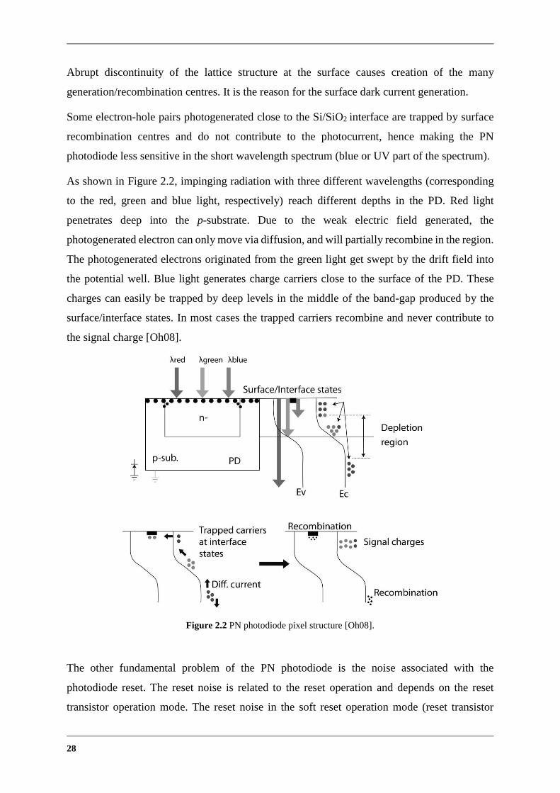
As shown in Figure 2.2, impinging radiation with three different wavelengths (corresponding
to the red, green and blue light, respectively) reach different depths in the PD. Red light
penetrates deep into the p-substrate. Due to the weak electric field generated, the
photogenerated electron can only move via diffusion, and will partially recombine in the region.
The photogenerated electrons originated from the green light get swept by the drift field into
the potential well. Blue light generates charge carriers close to the surface of the PD. These
charges can easily be trapped by deep levels in the middle of the band-gap produced by the
surface/interface states. In most cases the trapped carriers recombine and never contribute to
the signal charge [Oh08].
Figure 2.2 PN photodiode pixel structure [Oh08].
The other fundamental problem of the PN photodiode is the noise associated with the
photodiode reset. The reset noise is related to the reset operation and depends on the reset
transistor operation mode. The reset noise in the soft reset operation mode (reset transistor
29
operates in saturation) is reduced to approximately compared to the noise produced in
hard reset operation mode (reset transistor operates in a linear region) [Na05].
Introduced by the soft reset, image lag is one of the disadvantages. Additional injection of the
bias charge is needed before the soft reset operation (so called ″flashed reset″) in order to reduce
image lag [Na05].
2.2 Pinned Photodiode (PPD)
The pinned photodiode pixel was invented to overcome the major disadvantages of PN
photodiode structures: high dark current, high reset noise contribution, and limited sensitivity
in the short wavelength spectrum.
2.2.1 PPD Structure
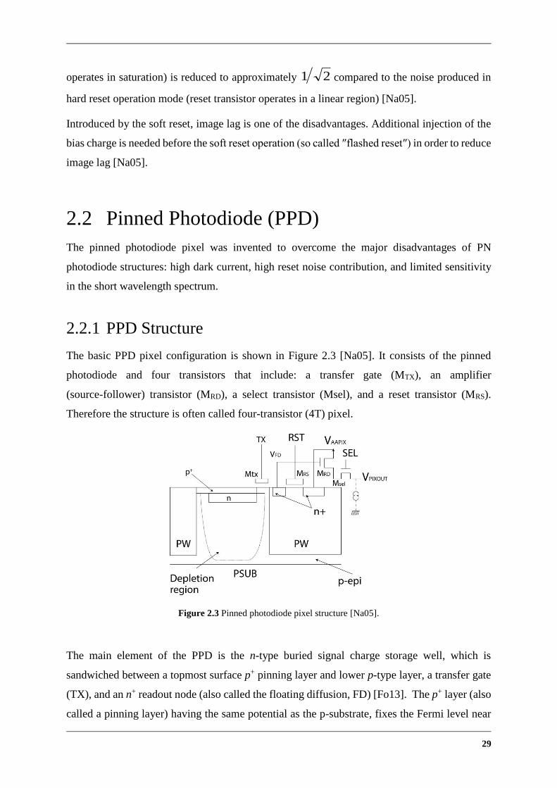
The basic PPD pixel configuration is shown in Figure 2.3 [Na05]. It consists of the pinned
photodiode and four transistors that include: a transfer gate (MTX), an amplifier
(source-follower) transistor (MRD), a select transistor (Msel), and a reset transistor (MRS).
Therefore the structure is often called four-transistor (4T) pixel.
Figure 2.3 Pinned photodiode pixel structure [Na05].
The main element of the PPD is the n-type buried signal charge storage well, which is
sandwiched between a topmost surface p+ pinning layer and lower p-type layer, a transfer gate
(TX), and an n+ readout node (also called the floating diffusion, FD) [Fo13]. The p+ layer (also
called a pinning layer) having the same potential as the p-substrate, fixes the Fermi level near
21

30
the silicon surface. The potential profile is thus bent. The accumulation region is then separated
from the surface and also from the trapping states [Oh08]. Carriers, photogenerated at short
impinging radiation wavelengths cannot recombine in this case with the surface/interface states,
they get directly swept to the accumulation region by the bent potential profile near the surface
(Fig. 2.4). The p+ layer is therefore not only responsible for bending the potential profile thus
producing a buried charge accumulation region, separated from the surface/interface trapping
states, but also “passivates” the defects located at the Si/SiO2 interface, that are the main source
of the dark current in a conventional PD.
Figure 2.4 Behaviour of photo-generated carriers in PPD [Oh08].
2.2.2 Advantages and Disadvantages of PPD Photodiodes
To achieve complete depletion in PPD pixels not only the p+ layer is required, but also a careful
design of the potential profile across the pixel, which entails correctly establishing fabrication
process parameters and precisely controlling pixel manufacturing.
Another drawback of PPD compared to the conventional PD is the presence of an additional
transistor (MTX) that reduces the fill factor (FF) of a pixel.
Having outstanding dark current performance due to the existence of the pinning layer and
being sensitive in short wavelength of the spectrum (UV and blue region), PPD shows good
noise performance. The suppression of the reset noise in PPD is achieved by using correlated
double sampling (CDS). Separation of the charge accumulation region from the charge readout
region via transfer gate (TX) gives the ability to readout the floating diffusion value twice: first
time after the reset phase and second time directly after the transfer of the charge carriers.
Subtraction of the both values minimizes reset noise.

31
Transfer of the charge carriers is one of the major issues in PPD. A potential barrier can appear
when the potential between the n-well and FD does not monotonically increase [Fo13]. Due to
the existence of this barrier some charges might never reach the FD and will therefore cause an
image lag. Additionally to the charge barrier, potential pockets that might appear across the
transfer path of the collected carriers also cause an image lag. Charge trapping in fast interface
states might be also critical [Bon12]. Trapped electrons then stay under the transfer gate during
the transfer phase and are released when the TX turns off. Trapped charges may be injected
then back to the PPD (spill-back). The charge transfer speed in a PPD pixel is limited by all the
mentioned imperfections and strongly depends on the geometry of the photodiode photoactive
area. For the pixels with small photoactive area, charge transfer is mostly defined by the
self-induced drift field (which dominates the initial transfer of charge carriers from the PPD
into the FD for the large signals) and fringing fields arising at the edges of the TX. For the
pixels with large photoactive areas, the charge transfer (due to the ″flat″ potential profile in PD)
becomes diffusion limited [Fo13] and can be significantly slower than in the case of the small
pixels.
2.3 Different Possibilities for Enhancing Charge
Transfer in PD
To increase the charge transfer speed in a large area PD and achieve complete transfer of the
signal electrons from the photoactive area into the readout node, a lateral electric field should
be created. Several ideas on how to improve the charge transfer in these types of pixel structures
were proposed by various scientific groups.
2.3.1 The Adjustment Shape of the Photodetector
In a low voltage operation the induced lateral electric field is very weak since the distance to
the TX is large. Therefore the speed of the charge transfer is decreasing and the electrons can
also be left in the photoactive area and create image lag.
Shin in his work [Sh10], in order to increase the charge transfer efficiency of charge carriers,
proposed using triangular shaped pixels. The weight of the pixel increases with the decrease of
the distance to the TX. The electrical force, formed due to the induced doping concentration
gradient across the pixel, pushes the electrons from the narrow part of the pixel in direction of
the TX.
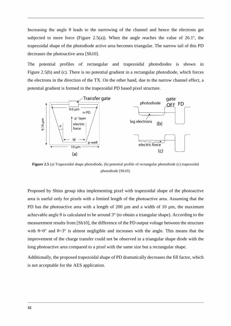
32
Increasing the angle θ leads to the narrowing of the channel and hence the electrons get
subjected to more force (Figure 2.5(a)). When the angle reaches the value of 26.1º, the
trapezoidal shape of the photodiode active area becomes triangular. The narrow tail of this PD
decreases the photoactive area [Sh10].
The potential profiles of rectangular and trapezoidal photodiodes is shown in
Figure 2.5(b) and (c). There is no potential gradient in a rectangular photodiode, which forces
the electrons in the direction of the TX. On the other hand, due to the narrow channel effect, a
potential gradient is formed in the trapezoidal PD based pixel structure.
Figure 2.5 (a) Trapezoidal shape photodiode, (b) potential profile of rectangular photodiode (c) trapezoidal
photodiode [Sh10].
Proposed by Shins group idea implementing pixel with trapezoidal shape of the photoactive
area is useful only for pixels with a limited length of the photoactive area. Assuming that the
PD has the photoactive area with a length of 200 µm and a width of 10 µm, the maximum
achievable angle θ is calculated to be around 3° (to obtain a triangular shape). According to the
measurement results from [Sh10], the difference of the PD output voltage between the structure
with θ=0° and θ=3° is almost negligible and increases with the angle. This means that the
improvement of the charge transfer could not be observed in a triangular shape diode with the
long photoactive area compared to a pixel with the same size but a rectangular shape.
Additionally, the proposed trapezoidal shape of PD dramatically decreases the fill factor, which
is not acceptable for the AES application.

33
2.3.2. P-epitaxial Layer with the Doping Gradient
Another idea was proposed by Cedric Tubert and his group [Tu09]: to add a doping gradient in
the epitaxial layer. This creates the pinning potential modulation. Induced electron drift
increases transfer speed of the generated electrons from the depth to the PPD depletion region
(Fig. 2.6). Horizontal drift pushes the electrons in direction of the readout node due to the
modulated pinning potential within the photoactive area.
The solution described in [Tu09] requires several additional pre-process steps to create an
epitaxial layer with a specific doping gradient. This adds additional costs to the manufacturing
process and in many cases is not possible to make at all.
Figure 2.6 Cross-section of the PD proposed by Tubert [Tu09].
2.3.3. Multiple N-doped Implantations
A multi-implant pinned-buried photodetector was proposed by by Kosonocky and Lowrance
to achieve a high-speed detection with nearly zero frame-to frame lag in [Ko96] [Ko97] [Jar01].
In the proposed design the graded potential is created by the variation of the doping
concentration in several implants. Several constant potential regions separated by the potential
steps of about 0.5 mV are formed in the photoactive area (Fig. 2.7).
Based on the model described in [Jar01], it can be speculated that the high speed PD would
require creation of as many constant potential regions (with minimal length and large diffusion

34
constant) in the photoactive area as possible. The electrons get transferred from each of the
regions inside the photoactive area with different speeds [Jar01].
Charge carriers transferred from the sections closer to the collecting gate require shorter period
of times to reach the gate, whereas the electrons from the periphery take longer. In a pixel with
a PA length of about 200 µm and a built n-well, as described in [Jar01], significant
non-uniformity in the charge transfer would be observed. In order to fabricate a multi-implant
pinned-buried PD with the length of the photoactive area of 200 µm, several implantation steps
with several additional masks is required. This brings additional complications to the design of
the n-well and as such additional costs to the production.
Figure 2.7 Cross sectional view of three n-type photodetector implant (a) graded potential profile (b) operation
of the PD [Jar01].
2.4 Introducing Lateral Drift-Field PD (LDPD)
A novel approach based on a lateral drift-field generated in a PD photoactive area using a
doping concentration gradient formed by a non-uniform lateral doping profile of an extra
designed n-well was proposed in [Dur10] [Mah10] (Fig. 2.8).
The induced lateral drift-field solves the transfer speed problem and also the image lag issue
commonly presented in a conventional PD.

35
2.4.1 LDPD Structure
The designed n-well is fabricated using single extra mask and a single extra n-type implantation
[Dur10]. The electrostatic potential created within the photoactive area increases in the
direction of the floating diffusion (FD) accelerating the charge carriers. The shape of the
non-uniformal doping profile is controlled by the geometry of the implantation mask and the
characteristic length of diffusion, directly proportional to the number and sort of the following
high-temperature annealing steps presenting in the 0.35µm CMOS process [Dur10].
Fabricated at one end of the n-well, a metal-oxide-semiconductor (MOS) capacitor-based
collection-gate (CG) remains biased at a certain voltage and induces an extra electrostatic
potential maximum in the system. The CG serves not only to additionally accelerate the
photogenerated charge carriers even more on their way to the readout node (RN), but also to
create a region of constant electrostatic potential from which the distribution of charge carriers
in any given direction by means of one or more transfer-gates might occur with the same
probability.
The CG is built on the same n-well (Fig. 2.8) and is considered to be a ″buried″ photogate.
Induced by the voltage applied to the CG, a potential maximum underneath the gate is therefore
located far away from the silicon surface reducing the amount of the transferred charge carriers
that can be trapped by the surface states, decreasing therefore the chance of the image lag to
appear and minimizing the amount of noise in the pixel output.
Figure 2.8 Schematic representation of the LDPD [Dur10].
Incorporated into the LDPD, a p+ layer ″pushes″ the potential maximum away from the silicon
surface thereby avoiding problems related to the surface dark current generation and reducing
the recombination rate of the minority carriers caused by the interface traps.

36
2.4.2 Advantages and Disadvantages of LDPD
The drift field generated by a laterally increasing dopant concentration of the LDPD n-well
accelerates the charge carriers in the direction of the readout node in the pixel. The charge
carrier transport is thus no longer diffusion limited and the charges are constantly drifted in
direction of the FD.
The proposed idea has several advantages compared to the other solutions described before:
non-uniformal doping concentration profile is formed in the LDPD with only one extra
mask, thus the manufacturing costs are not increasing
it has all the advantages of a PPD based pixel, and
it retains the benefits of being fabricated in CMOS technology.
The physical and design limitations difficulties related to the construction of such an n-well for
the large area PD are to be considered later in the text.
Fabricated on the same n-well, constantly biased CG creates an additional potential maximum
in the system also contributing to the charge acceleration process. The electrostatic potential
under the CG is kept constant, so the right bias voltage and geometry must be chosen for the
CG in order to further optimize the charge transfer.
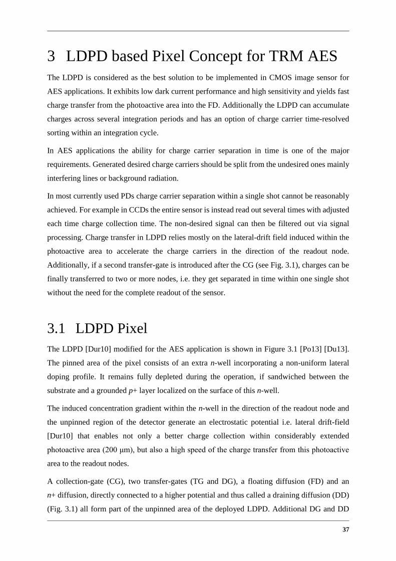
37
3 LDPD based Pixel Concept for TRM AES
The LDPD is considered as the best solution to be implemented in CMOS image sensor for
AES applications. It exhibits low dark current performance and high sensitivity and yields fast
charge transfer from the photoactive area into the FD. Additionally the LDPD can accumulate
charges across several integration periods and has an option of charge carrier time-resolved
sorting within an integration cycle.
In AES applications the ability for charge carrier separation in time is one of the major
requirements. Generated desired charge carriers should be split from the undesired ones mainly
interfering lines or background radiation.
In most currently used PDs charge carrier separation within a single shot cannot be reasonably
achieved. For example in CCDs the entire sensor is instead read out several times with adjusted
each time charge collection time. The non-desired signal can then be filtered out via signal
processing. Charge transfer in LDPD relies mostly on the lateral-drift field induced within the
photoactive area to accelerate the charge carriers in the direction of the readout node.
Additionally, if a second transfer-gate is introduced after the CG (see Fig. 3.1), charges can be
finally transferred to two or more nodes, i.e. they get separated in time within one single shot
without the need for the complete readout of the sensor.
3.1 LDPD Pixel
The LDPD [Dur10] modified for the AES application is shown in Figure 3.1 [Po13] [Du13].
The pinned area of the pixel consists of an extra n-well incorporating a non-uniform lateral
doping profile. It remains fully depleted during the operation, if sandwiched between the
substrate and a grounded p+ layer localized on the surface of this n-well.
The induced concentration gradient within the n-well in the direction of the readout node and
the unpinned region of the detector generate an electrostatic potential i.e. lateral drift-field
[Dur10] that enables not only a better charge collection within considerably extended
photoactive area (200 μm), but also a high speed of the charge transfer from this photoactive
area to the readout nodes.
A collection-gate (CG), two transfer-gates (TG and DG), a floating diffusion (FD) and an
n+ diffusion, directly connected to a higher potential and thus called a draining diffusion (DD)
(Fig. 3.1) all form part of the unpinned area of the deployed LDPD. Additional DG and DD

38
enable better time discrimination, differentiation and separation of “desired” charges from the
“undesired” ones.
Figure 3.1 Cross-sectional schematic view of the LDPD [Po13].
The CG creates a region of constant electrostatic potential within the LDPD n-well beneath it.
It assures equal probabilities of the charge transfer from this region to any of the sense nodes
placed aside it. Constantly biased CG creates an extra electrostatic potential maximum at the
system, which helps to additionally accelerate the generated charge carriers in direction of the
FD or the DD.
If the TG is correctly biased a potential barrier can be created within the n-well, thus preventing
the charge carriers being transferred to the FD during the charge readout cycle. On the other
hand during the charge collection cycle properly-biased TG enhances the lateral-drift field
mechanism and supports the charge carrier transfer into the FD.
The DG prevents the electrons from being drained out to connected constant high potential
during the collection cycle of the desired photogenerated charges and to drain the undesired
charge out of the pixel when necessary, providing the system with the time-controlled charge
collection ability.
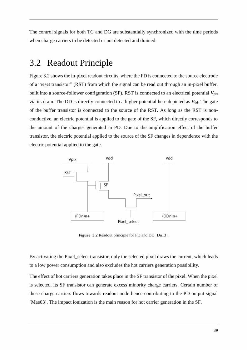
39
The control signals for both TG and DG are substantially synchronized with the time periods
when charge carriers to be detected or not detected and drained.
3.2 Readout Principle
Figure 3.2 shows the in-pixel readout circuits, where the FD is connected to the source electrode
of a “reset transistor” (RST) from which the signal can be read out through an in-pixel buffer,
built into a source-follower configuration (SF). RST is connected to an electrical potential Vpix
via its drain. The DD is directly connected to a higher potential here depicted as Vdd. The gate
of the buffer transistor is connected to the source of the RST. As long as the RST is non-
conductive, an electric potential is applied to the gate of the SF, which directly corresponds to
the amount of the charges generated in PD. Due to the amplification effect of the buffer
transistor, the electric potential applied to the source of the SF changes in dependence with the
electric potential applied to the gate.
Figure 3.2 Readout principle for FD and DD [Du13].
By activating the Pixel_select transistor, only the selected pixel draws the current, which leads
to a low power consumption and also excludes the hot carriers generation possibility.
The effect of hot carriers generation takes place in the SF transistor of the pixel. When the pixel
is selected, its SF transistor can generate excess minority charge carriers. Certain number of
these charge carriers flows towards readout node hence contributing to the PD output signal
[Mae03]. The impact ionization is the main reason for hot carrier generation in the SF.
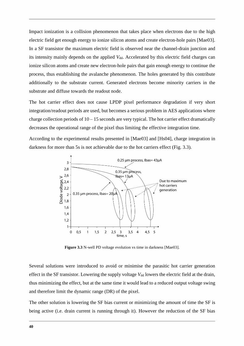
40
Impact ionization is a collision phenomenon that takes place when electrons due to the high
electric field get enough energy to ionize silicon atoms and create electron-hole pairs [Mae03].
In a SF transistor the maximum electric field is observed near the channel-drain junction and
its intensity mainly depends on the applied Vdd. Accelerated by this electric field charges can
ionize silicon atoms and create new electron-hole pairs that gain enough energy to continue the
process, thus establishing the avalanche phenomenon. The holes generated by this contribute
additionally to the substrate current. Generated electrons become minority carriers in the
substrate and diffuse towards the readout node.
The hot carrier effect does not cause LPDP pixel performance degradation if very short
integration/readout periods are used, but becomes a serious problem in AES applications where
charge collection periods of 10 – 15 seconds are very typical. The hot carrier effect dramatically
decreases the operational range of the pixel thus limiting the effective integration time.
According to the experimental results presented in [Mae03] and [Hs04], charge integration in
darkness for more than 5s is not achievable due to the hot carriers effect (Fig. 3.3).
Figure 3.3 N-well PD voltage evolution vs time in darkness [Mae03].
Several solutions were introduced to avoid or minimise the parasitic hot carrier generation
effect in the SF transistor. Lowering the supply voltage Vdd lowers the electric field at the drain,
thus minimizing the effect, but at the same time it would lead to a reduced output voltage swing
and therefore limit the dynamic range (DR) of the pixel.
The other solution is lowering the SF bias current or minimizing the amount of time the SF is
being active (i.e. drain current is running through it). However the reduction of the SF bias

41
current worsens the transistor performance and thus it cannot be considered as a good design
for the application in AES.
Considering all solutions listed above and their strength and weaknesses, the hot carrier effect
in the LDPD pixel can be reduced (in some cases almost eliminated) by decreasing the pixel
selection period: the select transistor gets activated only during the pixel readout phase.
3.3 Charge Transfer Mechanism in LDPD
The charge carrier transfer mechanism is shown more in detail in the Figure 3.4. Transfer and
readout mechanisms in LDPD for the AES application differ from the charge transfer
mechanisms used in standard imaging applications.
Charge carriers generated in the photoactive area of an LDPD are initially transferred via lateral
drift-field to the CG. If a high voltage is applied on the TG and a low voltage on the DG
(Fig. 3.4), electrons are drifted further in direction of the readout node. In case the application
of AES, integration and charge transfer are performed simultaneously to provide better transfer
by combining of the electrostatic potentials under the CG, TG and FD to accelerate the charge
transfer across the pixel.
Figure 3.4 Charge transfer in LDPD, integration phase [Ch13].
During the readout phase, low voltage is applied to TG and high voltage to DG, so that the
“unwanted” charges coming from the photoactive area and CG can get continuously drained to
the high potential Vdd. DG is also activated when the undesired charge carriers generated due to
the electromagnetic radiation from the plasma discharge (moment before the actual integration)
are to be drained out in order not to contribute to the output signal (Fig. 3.5).
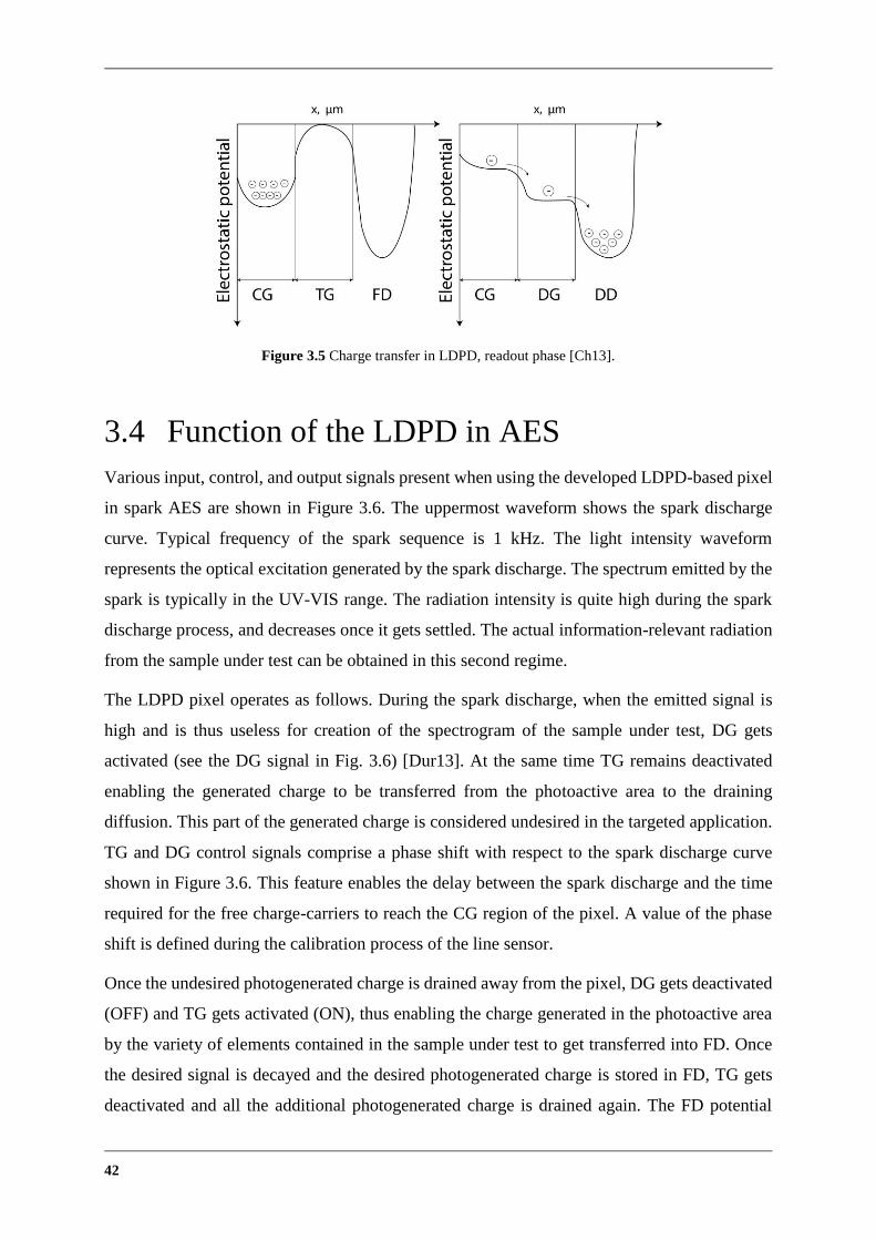
42
Figure 3.5 Charge transfer in LDPD, readout phase [Ch13].
3.4 Function of the LDPD in AES
Various input, control, and output signals present when using the developed LDPD-based pixel
in spark AES are shown in Figure 3.6. The uppermost waveform shows the spark discharge
curve. Typical frequency of the spark sequence is 1 kHz. The light intensity waveform
represents the optical excitation generated by the spark discharge. The spectrum emitted by the
spark is typically in the UV-VIS range. The radiation intensity is quite high during the spark
discharge process, and decreases once it gets settled. The actual information-relevant radiation
from the sample under test can be obtained in this second regime.
The LDPD pixel operates as follows. During the spark discharge, when the emitted signal is
high and is thus useless for creation of the spectrogram of the sample under test, DG gets
activated (see the DG signal in Fig. 3.6) [Dur13]. At the same time TG remains deactivated
enabling the generated charge to be transferred from the photoactive area to the draining
diffusion. This part of the generated charge is considered undesired in the targeted application.
TG and DG control signals comprise a phase shift with respect to the spark discharge curve
shown in Figure 3.6. This feature enables the delay between the spark discharge and the time
required for the free charge-carriers to reach the CG region of the pixel. A value of the phase
shift is defined during the calibration process of the line sensor.
Once the undesired photogenerated charge is drained away from the pixel, DG gets deactivated
(OFF) and TG gets activated (ON), thus enabling the charge generated in the photoactive area
by the variety of elements contained in the sample under test to get transferred into FD. Once
the desired signal is decayed and the desired photogenerated charge is stored in FD, TG gets
deactivated and all the additional photogenerated charge is drained again. The FD potential
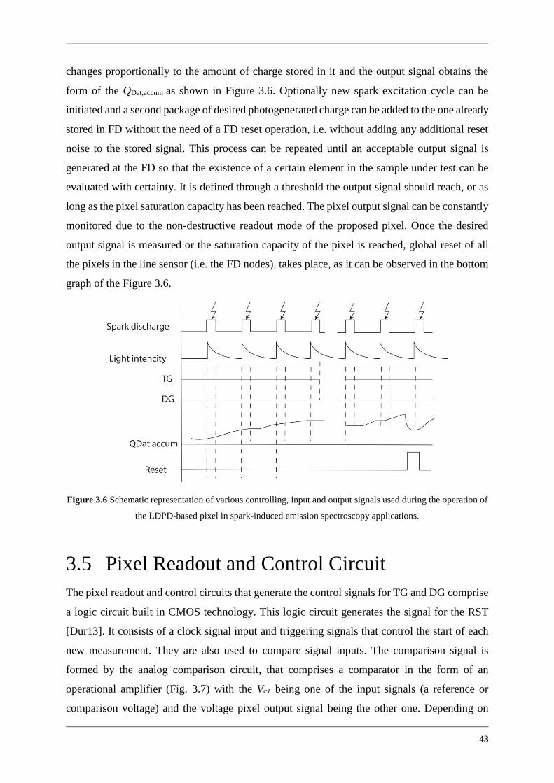
43
changes proportionally to the amount of charge stored in it and the output signal obtains the
form of the QDet,accum as shown in Figure 3.6. Optionally new spark excitation cycle can be
initiated and a second package of desired photogenerated charge can be added to the one already
stored in FD without the need of a FD reset operation, i.e. without adding any additional reset
noise to the stored signal. This process can be repeated until an acceptable output signal is
generated at the FD so that the existence of a certain element in the sample under test can be
evaluated with certainty. It is defined through a threshold the output signal should reach, or as
long as the pixel saturation capacity has been reached. The pixel output signal can be constantly
monitored due to the non-destructive readout mode of the proposed pixel. Once the desired
output signal is measured or the saturation capacity of the pixel is reached, global reset of all
the pixels in the line sensor (i.e. the FD nodes), takes place, as it can be observed in the bottom
graph of the Figure 3.6.
Figure 3.6 Schematic representation of various controlling, input and output signals used during the operation of
the LDPD-based pixel in spark-induced emission spectroscopy applications.
3.5 Pixel Readout and Control Circuit
The pixel readout and control circuits that generate the control signals for TG and DG comprise
a logic circuit built in CMOS technology. This logic circuit generates the signal for the RST
[Dur13]. It consists of a clock signal input and triggering signals that control the start of each
new measurement. They are also used to compare signal inputs. The comparison signal is
formed by the analog comparison circuit, that comprises a comparator in the form of an
operational amplifier (Fig. 3.7) with the Vc1 being one of the input signals (a reference or
comparison voltage) and the voltage pixel output signal being the other one. Depending on
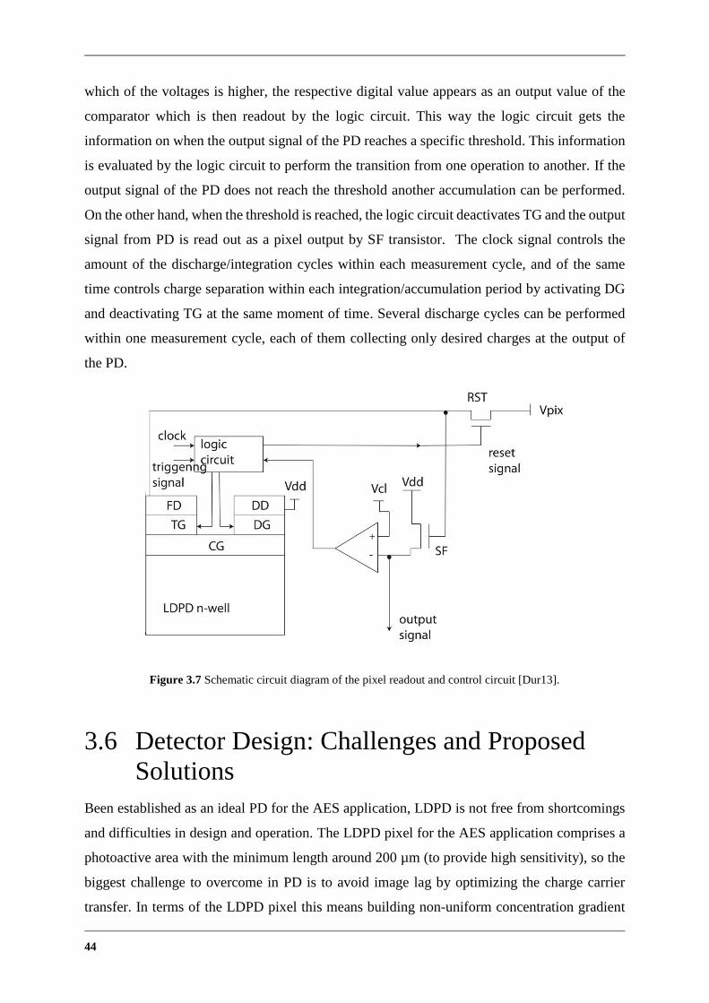
44
which of the voltages is higher, the respective digital value appears as an output value of the
comparator which is then readout by the logic circuit. This way the logic circuit gets the
information on when the output signal of the PD reaches a specific threshold. This information
is evaluated by the logic circuit to perform the transition from one operation to another. If the
output signal of the PD does not reach the threshold another accumulation can be performed.
On the other hand, when the threshold is reached, the logic circuit deactivates TG and the output
signal from PD is read out as a pixel output by SF transistor. The clock signal controls the
amount of the discharge/integration cycles within each measurement cycle, and of the same
time controls charge separation within each integration/accumulation period by activating DG
and deactivating TG at the same moment of time. Several discharge cycles can be performed
within one measurement cycle, each of them collecting only desired charges at the output of
the PD.
Figure 3.7 Schematic circuit diagram of the pixel readout and control circuit [Dur13].
3.6 Detector Design: Challenges and Proposed
Solutions
Been established as an ideal PD for the AES application, LDPD is not free from shortcomings
and difficulties in design and operation. The LDPD pixel for the AES application comprises a
photoactive area with the minimum length around 200 µm (to provide high sensitivity), so the
biggest challenge to overcome in PD is to avoid image lag by optimizing the charge carrier
transfer. In terms of the LDPD pixel this means building non-uniform concentration gradient

45
within the PA such that it would induce maximum electrostatic potential gradient and hence
maximum lateral-drift field that would drive the charge carriers from the photodiode to the
floating diffusion.
The n-well in LDPD should remain fully depleted during PD operation so the correctly chosen
doping profile of the n-well and p+ layer is necessary. High doping concentration of the n-well
brings along difficulties in a charge generation and transfer. Full depletion of the n-well
becomes a hard task, as well as transport and timing separation of the charge carriers.
To avoid charge trapping on the fast surface states located at the Si-SiO2 interface underneath
the gates, CG and TG are built in the form of buried photogate. This configuration ensures that
the n-well in LDPD is not stopping at the end of the photoactive area (PPD case), but coming
up to FD, overlapping with TG.
Design of the n-well mask is a complicated task in the case of LDPD. The potential barrier
created underneath TG by the incorrectly chosen geometry of the n-well could hamper the
transfer and cause an image lag. This problem could be avoided by careful modelling and
simulation of the electrostatic potential profile and the electron flow underneath the TG in the
LDPD.
Highly doped n-well also complicates the charge separation. Blocking the charge flow
underneath TG by applying low voltage on the gate (and thus creating the potential barrier)
becomes difficult. ″Unwanted″ charge carriers would then be transferred to the readout node
and contribute to the output signal.
Carefully selected applied voltages and length and width of CG and TG can effectively reduce
the image lag in the LDPD. To achieve that, applied voltages on the CG/TG should be chosen
in such a way that no electrostatic potential maximum is created under CG causing the potential
pocket. Induced fringing field underneath the gates will then additionally accelerate the charges
towards FD.
The geometry of the gates plays an especially large role when the dark current in the LDPD is
considered. Dark current (surface leakage current) can be dramatically reduced by the carefully
choosing size of the gates. The existence of the pinning layer decreases the dark current
generated within the photoactive area of the LDPD, so only the bulk diffusion leakage and dark
current generated within the depletion zone should be considered. Both of the components
strictly depend on the process quality and can be minimized by improving the process itself.

46
Crosstalk is a well-known problem in CMOS imagers. To avoid electrical crosstalk, charge
carriers in LDPD should always stay under the influence of the electric field. However, charges
generated outside of the depletion zone may diffuse to the neighbouring pixel. To avoid this in
LDPD the n-wells of the neighbouring pixels are separated by a deep p-well.
4 Characteristics of the LDPD pixel
Basic theory of the LDPD pixel is considered in the current chapter. A comprehensive study of
the pixel performance parameters is presented to understand the physical behaviour of the pixel
structure. Dark current is discussed, the major sources of the dark current in LPDP pixel
structure are presented together with measures proposed for its minimization. The spectral
response of the pixel and the charge carrier transfer characteristics within the pixel are
addressed and carefully investigated. Finally, an analysis of the crosstalk between neighbouring
pixel structures is briefly reviewed.
4.1 Performance Characteristics
Photons impinging the photoactive area of a pixel via a photoelectric effect create
electron-hole pairs within silicon. Absorption coefficient α of silicon depends strongly on the
wavelength and thus the energy of the incident light. For energies of impinging photons smaller
than the bandgap Eg (1.12 eV for silicon, considered at the potential maximum of the valence
band and the potential minimum of the conduction band), silicon is said to be transparent, as no
photoelectric effect can take place. For energies larger than the energy of the bandgap the
photoelectric effect does take place as the transmitted energy from the impinging photons
suffices for a scattered electron to make a transition to the conduction band.
As the energy of the incident light gets higher, i.e. the frequency of the impinging radiation also
gets higher (considering the wave-like behaviour of light). The scattering rate of the material
this impinging light interacts with also increases and thus the penetration depth (i.e. the depth
within the absorption material at which the energy of the impinging photon gets reduced to the
value of 1/e) decreases. The minimum energy required to induce photoelectric effect in silicon
is 1.12 eV at room temperature. This means that the cut-off frequency of the impinging light
(considering the wave-particle duality of light) for this effect to occur corresponds to the
impinging light is wavelength of 1.107 µm [Bla09].

47
4.1.1 Spectral Responsivity and Quantum Efficiency
The quantum efficiency η is commonly defined as the ratio of the amount of electron-hole pairs
(EHP) and the number of incident photons. It can be also viewed as the probability for one
impinging photon to generate one electron-hole pair. The quantum efficiency is always less
than 100% due to several reasons. First of all, due to losses caused by the Fresnel reflection of
the incident light at the surface of the device. Then due to the multiple reflections in thin layers
covering the photodiode and also absorption of the incident light either in the covering layers
or in the electrically inactive part of the semiconductor near the surface. And finally, due to the
absorption of impinging photons deep in the semiconductor, at a distance larger than the
diffusion length of the minority carriers, where charge carriers recombine before they can reach
a collection site and get separated from their accompanying holes.
If the generated photocurrent Iph is measured as the function of the incident light power P(W)
at the wavelength λ, then the corresponding optical sensitivity, defined as the amount of
photogenerated current Iph per unit of the impinging energy or optical power P (normally
measured in units of Ampere per Watt, A/W), is:
𝑂𝑆 =𝐼ph
𝑃, (4.1.1)
or relative to quantum efficiency:
𝑂𝑆 =𝑞𝜆
ℎ𝑐∙ 𝜂(𝜆), (4.1.2)
where h ≈ 6.63 × 10⁻³⁴ Js is the Plank's constant, q is the electron unit charge, is the
wavelength of the impinging light, and c ≈ 3 × 10⁸ m/s is the speed of light in vacuum.
The photogenerated electron-hole pairs in the pixel is separated from each other and collected
at a pixel collection site (normally denominated pixel sense-node (SN)) during a certain
photocurrent integration time (tint) and then converted using the SN capacitance CSN into a
signal equivalent potential output of the pixel.
The spectral responsivity R of such pixel structure can be defined as:
𝑅 = 𝑂𝑆 ∙ 𝐴ph𝐴SF
𝐶SN, V/(μJ/cm2). (4.1.3)
This pixel structure is a of so called active pixel structure type. This means that the
photogenerated electrical signal is at first amplified within the pixel using an in-pixel
48
source-follower (SF) amplification stage. In Equation 4.1.3 Aph is the photoactive area of the
pixel, and ASF is the SF "gain".
As it follows from the Equation 4.1.3 higher responsivity can be achieved by lowering the sense
node capacitance and increasing the optical sensitivity.
4.1.2 Conversion Gain
Floating diffusion converts generated charge packets into charge in voltage that can be buffered.
In the investigated LDPD pixel floating diffusion on the pixel is reset to a predetermined voltage
before integration starts. It is left floating during the charge integration period. After the charge
is collected on a pixel node, voltage change proportional to the charge is performed. This change
in voltage happens due to the charge packet Nsig on the charge sensing node is defined as:
𝑉FD =𝑞𝑁sig
𝐶SN, (4.1.4)
where CSN is the capacitance of the sense node in Farad and q is an elementary charge [Sua08].
The conversion gain (CG) typically refers to the output voltage variation of the pixel that
happens when a photo carrier is captured by the charge sensing node. This voltage variation is
associated with the charge sensing node, hence conversion gain is used as a measurement of
the capacitance of the charge sensing node.
The CG can be calculated as:
𝐶𝐺 =𝑞𝐴SF
𝐶SN, (μV/e−) (4.1.5)
where CSN
is the SN capacitance of the LDPD pixel, q is the electron charge, and ASF
is the
amplification of the source follower in voltage [Oh08].
The capacitance of the sense node mainly consists of the junction capacitance of the floating
diffusion, gate capacitance of the SF and parasitic capacitance associated with the node.
Conversion gain (CG) is the relationship between the amount of the collected electrons in the
pixel and the output analogue voltage obtained at the source follower. In other words conversion
gain defines the efficiency of the pixel in converting collected electrons into output voltage
signal.
The conversion gain (or overall system gain) and SN capacitance can be calculated using PTM
(see Appendix C). According to Equation 4.1.5 high conversion gain can be achieved by

49
lowering the capacitance of the sense node. The conversion gain becomes a crucial parameter
if small signals have to be detected.
4.1.3 Full Well Capacity (Saturation Capacity)
The full well capacity (FWC) defines the highest amount of charge that can be stored in the
pixel. The FWC can be expressed in the number of electrons and in this case is given by:
𝐹𝑊𝐶 =𝑉sat
𝐶𝐺, (4.1.6)
where Vsat
is the maximum output signal level.
4.1.4 SNR and Dynamic Range
The dynamic range (DR) is the ratio between the maximum pixel output signal (FWC) and
noise floor. It defines the ratio between the maximum and the minimum possible amount of
impinging radiation that can be detected by the pixel and expressed as:
𝐷𝑅 = 20 ∙ log 𝑁sat
𝑛read, (4.1.7)
here, Nsat is the full well capacity and nread is the referred input noise floor, expressed in electrons
(includes dark shot noise and readout noise).
Signal-to-noise is the ratio of the signal and the noise at a certain illumination level, in decibel:
𝑆𝑁𝑅 = 20 ∙ log 𝑁sig
𝑛, (4.1.8)
here, Nsig is the signal level in electrons at certain illumination level and n is the temporal
noise at the signal level Nsig [Na06].
4.1.5 Linearity
A straight line that is defined by an output level corresponding to a zero exposure and an output
level corresponding to a standard exposure is considered as an ideal characteristic of the CMOS
PD. Linearity error is defined as a deviation of a measured characteristic from the ideal
characteristic.
50
The photon-to-electron conversion is essentially a linear process, but the electron-to-signal
charge conversion (for example, charge collection efficiency) and the signal charge-to-output
voltage conversion could be nonlinear processes [Na06].
4.1.6 Noise Sources in LDPD
Several noise sources are identifiable in the LDPD pixel. They can be divided in to two main
categories: fixed pattern noise (FPN) and temporal noise.
4.1.6.1 Fixed Pattern Noise
Spatially fixed variations of the output signal from pixel to pixel are called fixed pattern noise
(FPN). They were a great concern for image quality in development every CMOS based imager.
Depending on the illumination conditions, light fixed pattern noise (photo response
non-uniformity, PRNU) and dark FPN (dark response non-uniformity, DRNU) are considered.
PRNU (photo response non-uniformity) is the variation of the responsivity between different
pixels computed over the pixel active area. Local variations in layer thickness and doping
impurities cause variations in the photogeneration process of the electron-hole pairs, which in
turn cause variations in the pixel voltage output. In-pixel transistor parameters, such as varying
threshold voltage, can vary from pixel to pixel due to the fabrication uniformity limitation, and
contribute to the PRNU.
DRNU (dark response non-uniformity) originates from the non-uniformities of the dark current
generated in each pixel. Non-uniform spatial patterns of impurity concentrations in the wafer,
temperature distribution within the pixel array area and in-pixel transistor parameters variation
are the main reasons of the dark current differences between different pixels.
4.1.6.2 Temporal Noise
There are several mechanisms responsible for temporal noise generation: photon shot noise,
dark current shot noise, reset noise, 1/f noise, and thermal (Johnson) noise.
4.1.6.2.1 Photon Shot Noise and Dark Current Shot Noise
The photon shot noise (PSN) is the main noise contribution factor at any illumination level. It
originates from the fluctuations in the number of the photons hitting the pixel photoactive area
that follows a Poisson distribution function. This is a physical phenomenon that cannot be
influenced in any way.
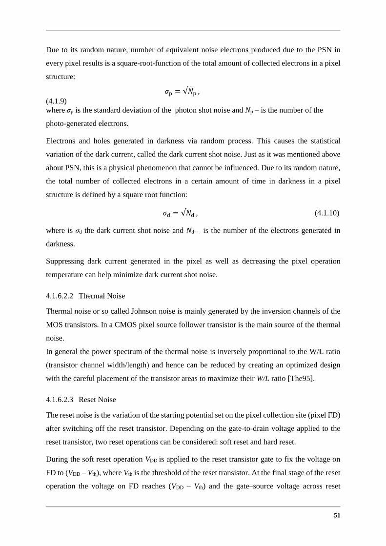
51
Due to its random nature, number of equivalent noise electrons produced due to the PSN in
every pixel results is a square-root-function of the total amount of collected electrons in a pixel
structure:
𝜎p = √𝑁p ,
(4.1.9)
where σp is the standard deviation of the photon shot noise and Np – is the number of the
photo-generated electrons.
Electrons and holes generated in darkness via random process. This causes the statistical
variation of the dark current, called the dark current shot noise. Just as it was mentioned above
about PSN, this is a physical phenomenon that cannot be influenced. Due to its random nature,
the total number of collected electrons in a certain amount of time in darkness in a pixel
structure is defined by a square root function:
𝜎d = √𝑁d , (4.1.10)
where is σd the dark current shot noise and Nd – is the number of the electrons generated in
darkness.
Suppressing dark current generated in the pixel as well as decreasing the pixel operation
temperature can help minimize dark current shot noise.
4.1.6.2.2 Thermal Noise
Thermal noise or so called Johnson noise is mainly generated by the inversion channels of the
MOS transistors. In a CMOS pixel source follower transistor is the main source of the thermal
noise.
In general the power spectrum of the thermal noise is inversely proportional to the W/L ratio
(transistor channel width/length) and hence can be reduced by creating an optimized design
with the careful placement of the transistor areas to maximize their W/L ratio [The95].
4.1.6.2.3 Reset Noise
The reset noise is the variation of the starting potential set on the pixel collection site (pixel FD)
after switching off the reset transistor. Depending on the gate-to-drain voltage applied to the
reset transistor, two reset operations can be considered: soft reset and hard reset.
During the soft reset operation VDD is applied to the reset transistor gate to fix the voltage on
FD to (VDD – Vth), where Vth is the threshold of the reset transistor. At the final stage of the reset
operation the voltage on FD reaches (VDD – Vth) and the gate–source voltage across reset
52
transistor becomes less than Vth, the reset transistor is in subthreshold region. During the soft
reset the voltage on FD slowly reaches (VDD – Vth) [Oh08].
The reset noise voltage in the case of soft reset is given by:
𝑉soft reset = √𝑘𝑇
2𝐶, (4.1.11)
here C is FD capacitance, k is Boltzmann’s constant and T is the absolute temperature.
In the case of hard reset, the applied gate-to-drain voltage is always higher than the threshold,
the reset transistor is thus always operating above the threshold, reset finishes quickly.
The reset noise in this case is defined as:
𝑉hard reset = √𝑘𝑇
𝐶. (4.1.12)
The kTC noise during hard reset operation is increased by a factor of due to the possible
bidirectional movement of the charges between FD node and reset voltage node.
The major disadvantage of the soft reset operation is the image lag and the advantage is the
reduced kTC noise. The reset noise does not depend on the number of interacting photons and
is only dominant at low signal levels.
A readout technique called correlated double sampling (CDS) is used to minimize the kTC
noise. It consists of sampling and subtracting the output voltage on FD after the pixel reset and
then immediately after the end of the pixel illumination phase. This operation can be performed
using an integrated solution on-the-chip, or once both values are read out outside the chip. No
integrated CDS is implemented in the LDPD pixel output circuit due to the application
requirements.
4.1.6.2.4 1/f or Flicker Noise
Flicker noise or 1/f noise is a low frequency noise coming mainly from the SF transistor [Fi03].
Interaction of the interface states located at the Si-SiO2 interface of the MOS transistor with the
electrons in the inversion channel causes fluctuations in the voltage at the output of the SF. This
is the main reason of flicker noise.
By using depletion type MOS transistor as SF interactions between the interface states and
charges can be kept at a low level. The inversion channel in this type of device is pushed
somewhat deeper in the silicon [The95]. The flicker noise suppression could be also achieved
by introducing CDS [Wa08].
2
53
4.2 Dark Current
Dark current gets generated when a sensor operates in complete darkness. It is one of the major
parameters to consider in a large area CMOS line sensor aimed for AES application. Dark
current lowers the charge capacitance available to the photo carriers, hence limiting the
potential integration time, which in AES sometimes is required to be of the order to several
seconds. Additionally, dark current variation in space and time produces spatial and temporal
non-uniformity in the output signal (former leads to the fixed pattern noise, latter one- to the
dark current shot noise). There are several regions in the LDPD pixel that contribute to the dark
current generation: the neutral part of the p-epitaxial layer below the n-well, the Si-SiO2
interfaces, and the depletion zone in the pixel PA itself (Fig. 4.1).
Figure 4.1 Cross section of the LDPD pixel with demonstrating of the dark current mechanism.
The charge carriers generated under conditions with no illumination within the depletion region
of the pixel contribute to the so-called depletion dark current. Diffusion of minority carriers
generated within the p-epitaxial layer below the n-well is called diffusion dark current; dark
current generated at the Si-SiO2 interface is known as the surface leakage current.
4.2.1 Depletion Dark Current
In indirect-bandgap semiconductors such as Si, the current generation in the absence of light is
very difficult, electron needs a help of a medium in order to jump from the valence zone to the
conduction zone. This can be achieved by electron transitions via bulk traps present within the
bandgap. The defect level (trap, or in other words a localized energy state) is the result of an

54
imperfections in the fabrication process. The defects which can be present in silicon are the
point defects for example Schottky defect, Frenkel defect, interstitial defect, lattice defects such
as dislocations, and bulk defects, i.e. clusters of vacancies.
The indirect transition in silicon happens in the following way (Fig. 4.2): an electron from the
valance band first jumps to the defect level (the required energy for this transition is much less
than 1.12 eV, bandgap value of the Si); a hole is generated in the valance band; an electron can
now be further emitted from the defect energy state to the conduction band (this transition is
seen as the electron generation). As a result, free electrons and holes are created, thus forming
part of the dark current flowing in the pixel.
The inverse transition can occur where an electron falls first from the conduction band into the
existing trap offering an allowed energy level within the bandgap of Si, and then further to the
valance band where it gets recombined. Holes can also be captured by the trap level, thus
recombining with electrons that happen to appear there, too.
Figure 4.2 Carrier generation and recombination process via a trap level in the band gap.
Recombination/generation via bulk traps is the dominant transition in Si. The net transition rate
is described by the Shockley-Read-Hall statistics [Sz07]:
𝑈 =𝜎n∙𝜎p∙𝜐th∙𝛮t(𝑝𝑛−𝑛i
2)
𝜎𝑛[𝑛+𝑛iexp (𝐸t−𝐸i
𝑘𝑇)]+𝜎p[𝑝+𝑛iexp (
𝐸t−𝐸i𝑘𝑇
)], (4.2.1)
where σn and σp are the electron and hole capture cross-section, respectively, Et is trap energy,
Nt is trap density, υth is thermal velocity, p is the hole concentration, n is the electron
concentration , ni is intrinsic carrier concentration , k is Bolzmann’s constant, and T is the
absolute temperature.
From the Equation 4.2.1, it follows that the net transition rate is maximised when the trap level
energy is equal to the middle gap Et=Ei. In this case, the Equation 4.2.1 simplifies to:

55
𝑈 =𝜎n∙𝜎p∙𝜐th∙𝛮t(𝑝𝑛−𝑛i
2)
𝜎n[𝑛+𝑛i]+𝜎p[𝑝+𝑛i], (4.2.2)
The lifetime of electron and holes can then be derived as:
𝜏n =1
𝜎n𝜐th𝑁t, (4.2.3)
𝜏p =1
𝜎p𝜐th𝑁t, (4.2.4)
The lifetime of the charge carriers is inversely proportional to the trap density Nt and can then
be derived as:
𝜏 =𝜎n+σp
𝜎n𝜎p𝜐th𝑁t, (4.2.5)
Under the condition of thermal non-equilibrium, when pn<ni2, generation of carriers will occur
with the higher probability than recombination. The generation rate from Equation 4.2.2 can
then be rewritten as:
𝑈 =−𝜎n∙𝜎p∙𝜐th∙𝛮t𝑛i
𝜎n[1+𝑛/𝑛i]+𝜎p[1+𝑝/𝑛i]= −
𝑛i
𝜏g, (4.2.6)
where the generation carrier lifetime τg is equal to:
𝜏g =1+(𝑛/𝑛i)
𝜎p𝜐th𝑁t+
1+(𝑝/𝑛i)
𝜎n𝜐th𝑁t= (1 +
𝑛
𝑛i) 𝜏p + (1 +
𝑝
𝑛i) 𝜏n. (4.2.7)
The generation lifetime can be much larger than the recombination lifetime, while both p and n
are much smaller then ni.
The current density due to the trap-induced thermal generation in the depletion region of the
photodiode can then be calculated:
Jgeneration = ∫ 𝑞|𝑈|d𝑥 ≈ 𝑞|𝑈|𝑊D
0𝑊D ≈
𝑊D𝑞𝑛i
𝜏g, (4.2.8)
where WD is the depletion-layer width.
As it follows from the Equation 4.2.8 the generation current depends on the width of the
depletion layer, intrinsic carrier concentration ni, and the generation carrier life time τg.
If the generation carrier life time weakly depends on temperature, then the depletion current
follows temperature dependence of the ni [Sz07]:
𝑛i = √𝑁C𝑁Vexp (−𝐸g
2𝑘𝑇), (4.2.9)
56
where Nc is the effective density of states in the conductive band and Nv is the effective density
of states in the valance band.
At the same time:
𝑁C = 2(2𝜋𝑚de𝑘𝑇
ℎ2 )3
2, (4.2.10)
𝑁V = 2(2𝜋𝑚dh𝑘𝑇
ℎ2 )3
2, (4.2.11)
where mde and mdh are the electron and hole effective mass respectively and h is the Planck’s
constant. Combining Equation 4.2.10, 4.2.11, 4.2.9 and 4.2.8, it can be shown that the depletion
current has (-Eg/2) dependence on temperature.
At the given temperature, the depletion current is proportional to the depletion layer width,
which in turn depends on the applied reverse bias and junction doping profile.
One method to reduce the depletion dark current is to narrow the depletion region. However,
this at the same time reduces photodiode spectral sensitivity. Process-dependent amount of the
defects in silicon should be also reduced in order to decrease the depletion dark current.
Narrowing the depletion zone can lead to the tunnelling effect, when electrons move from the
valance band into the conduction band and become a part of the overall dark current of the
system. There may occur three main tunnel channels that: direct inter-band tunnelling, when
the electrons tunnel directly from the valence band into the conduction band; tunnelling via the
deep-level trap state; and thermal excitation into a surface state followed by a tunnelling
transition into the conduction band [Bre99].
When the potential barrier is sufficiently thin (induced by a large applied reverse bias) a
significant current begins to flow due to the band-to-band (inter-band) tunnelling.
The band-to-band tunnelling is defined as:
Jtunneling =√2𝑚∗𝑞3𝜁𝑉
4𝜋2ℏ2√𝐸gexp (−
4√2𝑚∗𝐸g3/2
3𝑞𝜉ℏ), (4.2.12)
where m* is the effective mass, ζ is the electric field across the junction, Eg is the band gap
energy, q is the electron charge, is the reduced Planck’s constant, V is the applied voltage
across the depletion region.
As it could be seen from the Equation 4.2.12 lowering the applied voltage or reducing the electric
field applied across the depletion region can effectively reduce the tunneling current.

57
4.2.2 Diffusion (Bulk) Dark Current
The process of diffusion occurs in the presence of the gradient of carrier concentration. Due to
the diffusion process the charge carriers move from the region of high concentration into the
region of low concentration, thus driving the system to the state of uniformity. The diffusion
current is the result of minority carriers generated in the bulk diffusing into the pixel depletion
zone, and being collected in the potential well, contributing in this way to the overall system
dark current [Bre99]. At the boundary of a p-n junction the minority carrier concentration under
reverse bias is lower than that in the neutral region. The diffusion current flows due to both the
hole concentration gradient in the n-type region and the electron concentration gradient in the
p-type region. Moreover, as soon as the voltage is applied, the minority carrier concentration
in both the p-type side and n-type side changes. The p-n product becomes no longer equal ni2
and is given by:
𝑝𝑛 = 𝑛i2exp (
𝐸Fn−𝐸Fp
𝑘𝑇), (4.2.13)
where EFn
and EFp
are the quasi-Fermi levels for electrons and holes, respectively. The
difference between EFn
and EFp
is related to carrier concentrations. The carrier diffusion then
tries to restore the system to the concentration equilibrium [Sz07].
The diffusion current can be calculated as follows [Sz07]:
𝐽n = 𝑞𝐷nd∆𝑛
d𝑥, (4.2.14)
𝐽p = −𝑞𝐷pd∆𝑝
d𝑥, (4.2.15)
where Dn is the diffusion coefficient of electrons, Dp is the diffusion coefficients of holes, p is
the hole concentration, n is the electron concentration, and q is the electron charge.
The diffusion coefficient is derived from the following equation considering the n-type
semiconductor with non-uniform doping concentration and with no externally applied voltage:
𝑞𝑛𝜇n𝜉 = 𝑞𝐷nd𝑛
d𝑥. (4.2.16)
The electric field created by the nonuniform doping can be described by ζ = dEc/qdx. After
certain transformation, the diffusion coefficients can be derived from (4.2.16):
𝐷n = (𝑘𝑇
𝑞)𝜇n. (4.2.17)
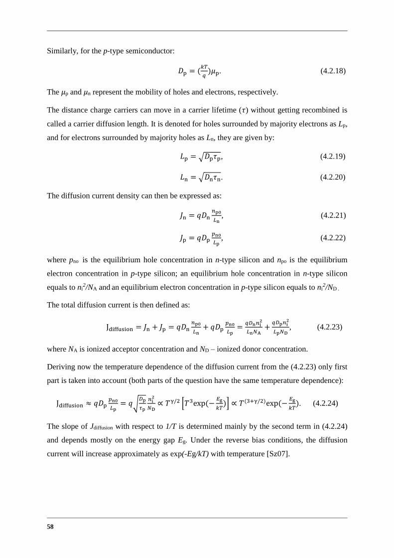
58
Similarly, for the p-type semiconductor:
𝐷p = (𝑘𝑇
𝑞)𝜇p. (4.2.18)
The μp and μn represent the mobility of holes and electrons, respectively.
The distance charge carriers can move in a carrier lifetime (τ) without getting recombined is
called a carrier diffusion length. It is denoted for holes surrounded by majority electrons as Lp,
and for electrons surrounded by majority holes as Ln, they are given by:
𝐿p = √𝐷p𝜏p, (4.2.19)
𝐿n = √𝐷n𝜏n. (4.2.20)
The diffusion current density can then be expressed as:
𝐽n = 𝑞𝐷n𝑛p0
𝐿n, (4.2.21)
𝐽p = 𝑞𝐷p𝑝n0
𝐿p, (4.2.22)
where pno is the equilibrium hole concentration in n-type silicon and npo is the equilibrium
electron concentration in p-type silicon; an equilibrium hole concentration in n-type silicon
equals to ni2/NA and an equilibrium electron concentration in p-type silicon equals to ni
2/ND .
The total diffusion current is then defined as:
Jdiffusion = 𝐽n + 𝐽p = 𝑞𝐷n𝑛p0
𝐿n+ 𝑞𝐷p
𝑝n0
𝐿p=
𝑞𝐷n𝑛i2
𝐿n𝑁A+
𝑞𝐷p𝑛i2
𝐿p𝑁D, (4.2.23)
where NA is ionized acceptor concentration and ND – ionized donor concentration.
Deriving now the temperature dependence of the diffusion current from the (4.2.23) only first
part is taken into account (both parts of the question have the same temperature dependence):
Jdiffusion ≈ 𝑞𝐷p𝑝n0
𝐿p= 𝑞√
𝐷p
𝜏p
𝑛i2
𝑁D∝ 𝑇γ/2 [𝑇3exp (−
𝐸g
𝑘𝑇)] ∝ 𝑇(3+γ/2)exp (−
𝐸g
𝑘𝑇). (4.2.24)
The slope of Jdiffusion with respect to 1/T is determined mainly by the second term in (4.2.24)
and depends mostly on the energy gap Eg. Under the reverse bias conditions, the diffusion
current will increase approximately as exp(-Eg/kT) with temperature [Sz07].
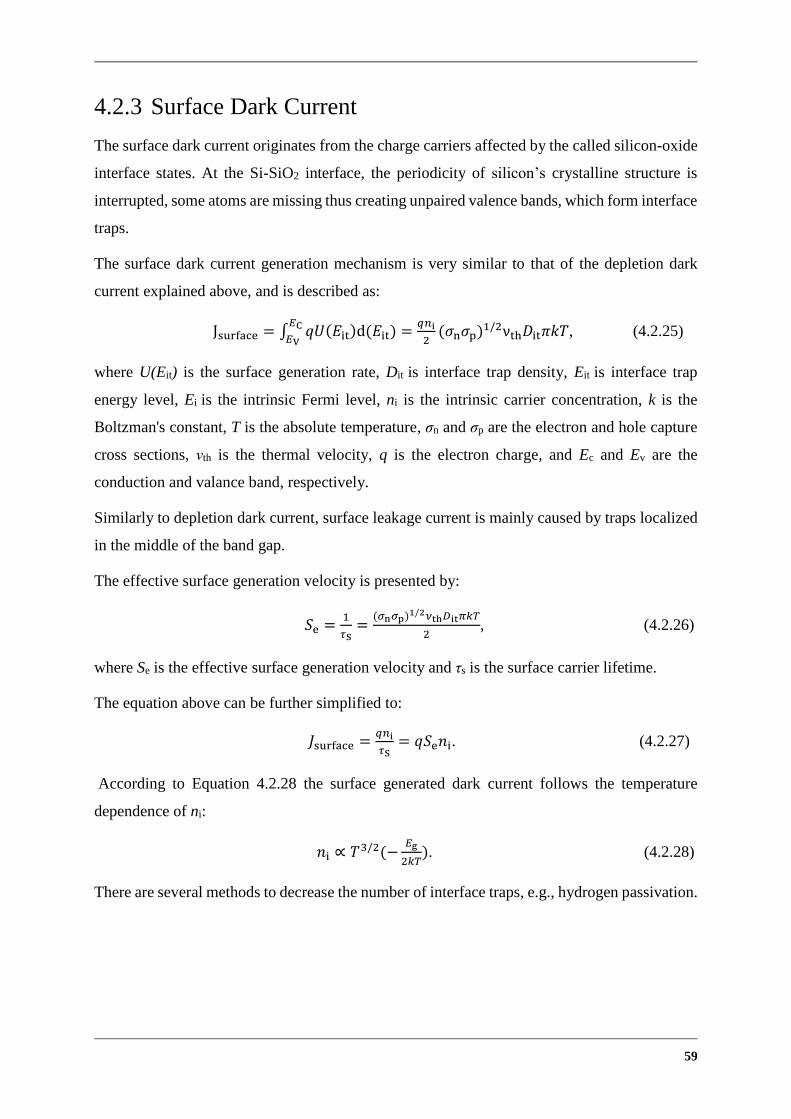
59
4.2.3 Surface Dark Current
The surface dark current originates from the charge carriers affected by the called silicon-oxide
interface states. At the Si-SiO2 interface, the periodicity of silicon’s crystalline structure is
interrupted, some atoms are missing thus creating unpaired valence bands, which form interface
traps.
The surface dark current generation mechanism is very similar to that of the depletion dark
current explained above, and is described as:
Jsurface = ∫ 𝑞𝑈(𝐸it)d(𝐸it)𝐸C
𝐸V=
𝑞𝑛i
2(𝜎n𝜎p)1/2νth𝐷it𝜋𝑘𝑇, (4.2.25)
where U(Eit) is the surface generation rate, Dit is interface trap density, Eit is interface trap
energy level, Ei is the intrinsic Fermi level, ni is the intrinsic carrier concentration, k is the
Boltzman's constant, T is the absolute temperature, σn and σp are the electron and hole capture
cross sections, νth is the thermal velocity, q is the electron charge, and Ec and Ev are the
conduction and valance band, respectively.
Similarly to depletion dark current, surface leakage current is mainly caused by traps localized
in the middle of the band gap.
The effective surface generation velocity is presented by:
𝑆e =1
𝜏S=
(𝜎n𝜎p)1/2𝜈th𝐷it𝜋𝑘𝑇
2, (4.2.26)
where Se is the effective surface generation velocity and τs is the surface carrier lifetime.
The equation above can be further simplified to:
𝐽surface =𝑞𝑛i
𝜏S= 𝑞𝑆e𝑛i. (4.2.27)
According to Equation 4.2.28 the surface generated dark current follows the temperature
dependence of ni:
𝑛i ∝ 𝑇3/2(−𝐸g
2𝑘𝑇). (4.2.28)
There are several methods to decrease the number of interface traps, e.g., hydrogen passivation.

60
4.2.4 Dark Current in the LDPD Pixel
The total dark current in the LDPD is combined from several dark current sources located in
different parts of the pixel. The dark current generated within the photoactive region of the
LDPD pixel includes the dark current that originates in the depletion region of the p-n junction
(depletion dark current), the one that comes from epitaxial layer (diffusion dark current) and
the dark current from the silicon surface (surface dark current) (Fig. 4.3).
The diffusion dark current is caused by the bulk defects and depends mainly on CMOS process
itself. Addition of the epitaxial layer with the width of about 15 µm avoids the minority carrier
thermally generated in highly-doped silicon bulk from reaching depletion region, hence the
diffusion dark current in 0.35 µm CMOS process is mainly depends on the amount of impurities
in a lowly doped p-epitaxial layer [Du09].
The depletion dark current depends on the width of the depletion region. Hence gets directly
influenced by the impurity concentration of the n-well implant. With higher implantation doses
n-well diffuses deeper into the bulk and the depletion zone, in case the entire n-well is depleted
(which is the goal), gets much wider causing the depletion dark current to increase.
Figure 4.3 Cross section of the LDPD pixel (photoactive area).
The LDPD pixel employs a pinned-photodiode structure for its photoactive area. A heavily
doped p+ pinning layer is placed on top of the LDPD n-well to minimize the surface generated
dark current by satisfying the dangling bonds on the surface and increase the recombination
rate of carriers thermally generated in this region. The p+ pinning layer is used to pin or fill the
interface traps at the Si-SiO2 surface with holes [Th06].
61
Another component of the dark current is related to the sidewalls and edges of the field oxide
(periphery component). Field oxide (FOX) is used to isolate the active areas of the pixel. It is
formed using a method called local oxidation of silicon (LOCOS). The creation of the FOX
includes several steps: growing the field oxide (usually at temperatures above 950°), deposition,
and etching. The fabrication of these structures introduces mechanical stress into the pixel and
causes dislocations along FOX resulting in a high dark current.
The sidewalls and edges of FOX in the LDPD pixel are separated from the depletion region by
the p-well, which has relatively high doping density. Thermally generated electrons at the side
of the field oxide region are then recombined with the majority carriers of the p-well. Increasing
the distance between FOX and pixel PA i.e. LDPD n-well can significantly reduce the dark
current induced by the defective sidewalls and edges. Similarly technological solution to
suppress the dark current generated in the isolation structure region was proposed and
experimentally investigated by S-W. Han and E.Yoon in [Ha05] [Ha06].
It was shown by Kwon during the characterization of the large area square PPD and long
periphery finger type diode, that the dark current generated from the sidewall regions is much
higher than those at the bulk and surface regions [Kw06]. In this work it was demonstrated that
the dark current can be successfully suppressed in the PPD-type photodiode by the p+ pinning
layer and that the sidewall junction leakage current increases dramatically due to small variation
of the p-well region.
Transfer and collection gate regions in the LDPD pixel also viewed as the sources of the surface
generated dark current (Fig. 4.4).
Figure 4.4 Cross section of the LDPD pixel (TG and CG region).
62
Only a small part of the dark current generated from the collection gate region can be
successfully suppressed. The tail of the p+ region on the surface of the PA can passivate the
interface traps from the depletion region formed near the surface of the CG. The depletion zone
underneath CG is in this case isolated from the Si-SiO2 surface hence the surface generated
dark current is reduced.
The floating diffusion area contains highly doped n+ implantation fabricated within a p-well
(Fig. 4.5). The FD depletion region touches SiO2 on the surface and FOX. Additionally, the
contact-etching process and high-dose implantation result in process-induced damage. These
are the main causes of the dark current in FD area [Kw06].
When the integration period during the normal operation of the floating diffusion node is short,
the dark current generated in this region of the LDPD pixel is almost negligible. As the
integration time increases, the surface-generated and bulk-generated currents are enhanced,
strongly contributing to the total dark current generated inside the LDPD pixel.
Further minimization of FD-generated dark current in the LDPD pixel could be achieved by
introducing a new p-well structure, which can separate the sidewalls of the FOX from the
depletion region of the LDPD n-well.
Figure 4.5 Cross section of the LDPD pixel (FD region).
The FOX is also used to separate TG from the DG nodes, as well as FD from DD in the pixel.
A deep p-well is created to passivate the interface traps at the FOX sidewalls (Fig. 4.6).

63
Figure 4.6 Cross section of the LDPD pixel and the demonstration of the dark current mechanism (in control
electrodes area).
The dark current in the LDPD pixel can also be reduced by a specially constructed passivation
layer. Silicon Nitride (SiN) passivation films contain a high concentration of hydrogen, that can
be released during the forming gas annealing, and is able to diffuse out into the silicon,
deactivating some of the electrically active defects [Be05]. The composition of the SiN plays a
significant role in the dark current reduction. Lower mean dark currents were obtained using
SiN-based passivation layers allowing for the highest hydrogen desorption [Be05]. Regolini in
[Re07] draws a conclusion that the higher the SiN density is the better the defects passivation
gets.
4.3 Charge transfer
To analyse the charge transfer in large area LDPD pixels several mechanisms should be taken
into account, such as thermal diffusion, self-induced drift, so called lateral drift-field, and
fringing field-induced transport.
4.3.1 Thermal Diffusion of the Charge Carriers
Generally, thermal diffusion refers to a charge redistribution process. Charge carriers tend to
move from region with a high concentration of carriers to the region of low concentration
[Sz07]. The effect of thermal diffusion was first studied by Kim [Ki71] and then expanded on

64
by Carnes [Ca71]. He introduced the concept of the current-density relation as a continuity
equation.
The diffusion current is given by:
𝐽𝑑 = 𝑞𝐷𝑛𝛿𝑄𝑛(𝑦,𝑡)
𝛿𝑦, (4.3.1)
where Dn – diffusion coefficient and Qn(y,t) – charge distribution as a function of position and
time.
The continuity equation, according to [Ca71]:
𝛿𝑄𝑛(𝑦,𝑡)
𝛿𝑡=
𝛿𝐽(𝑦,𝑡)
𝛿𝑦, (4.3.2)
connects the amount of charge to be transferred with the current density [The95]. Putting
together Equation 4.3.1 and 4.3.2 we get:
𝛿𝑄𝑛(𝑦,𝑡)
𝛿𝑡=
𝛿
𝛿𝑦(𝑞𝐷𝑛
𝛿𝑄𝑛(𝑦,𝑡)
𝛿𝑦). (4.3.3)
The solution is found as [The95]:
𝑄𝑛(𝑡) =8
𝜋2 𝑄𝑛(0)𝑒𝑥𝑝 [−𝜋2𝐷𝑛𝑡
4𝐿2 ], (4.3.4)
𝑄𝑛(𝑡) =8
𝜋2 𝑄𝑛(0)𝑒−𝑡/𝜏TD, (4.3.5)
where Qn(t) - charge at time t; Qn(0) - initial charge; τTD- diffusion time constant and L - transit
length .
The diffusion coefficient is related to the electron mobility µn as [Sz07]:
𝐷𝑛 =𝑘𝑇
𝑞𝜇𝑛. (4.3.6)
And the diffusion time constant from (4.3.4):
𝜏TD =4𝐿2
𝜋2𝐷𝑛. (4.3.7)
As it follows from Equation 4.3.4 the decay of the charges due to thermal diffusion is
exponential. The time constant of diffusion mechanism is inversely proportional to the diffusion
coefficient Dn and directly proportional to the square of the transit length L. Thus in order to
minimize the diffusion transfer time, L should be small.

65
4.3.2 Self-induced Drift Field
Self-induced drift (SID) is caused by the effect charge carriers have on themselves. A gradient
in the charge concentration is built up by the charge carriers of the same type when they start
repelling equal charges to rearrange their concentration so that the gradient across the pixel is
zero. This reordering takes place throughout the electric field generated by the gradient in
charge distribution [En70].
The continuity equation for the case of self-induced drift field can be rewritten as:
δ𝑄n(𝑦,𝑡)
δ𝑡=
δ𝐽
δ𝑦(𝑄n𝜇n𝐸s), (4.3.8)
where Es is the electric field, generated due to the presence of the charge gradient. This charge
gradient causes a change in a surface potential that creates an electric field [En70]. Surface
potential can be computed using one-dimensional Poisson equation. The self-induced field can
then be found as [The95]:
𝐸S(y) =δ𝜙S
δ𝑦=
δ𝜙S
δ𝑄n∙
δ𝑄n
δ𝑦 . (4.3.9)
The relation between the surface potential ϕs and the inversion charge Qn is defined as:
𝜙S = 𝜙SDD +𝑄n
𝐶OX+𝐶D , (4.3.10)
where ϕSDD is the surface potential in the case of empty well, Cox is the oxide capacitance and
CD is the depletion capacitance. Combining the Equations 4.3.9-4.3.10 we get:
δ𝑄n(𝑦,𝑡)
δ𝑡=
δ
δy(
𝑄n𝛽
𝐶OX+𝐶D) ∙ 𝐷n ∙
δ𝑄n(𝑦,𝑡)
δ𝑦, (4.3.11)
where 𝛽 =𝑞
𝑘𝑇. (4.3.12)
The movement of the charge carriers due to the self-induced drift field is similar to the thermal
diffusion transport.
This two processes can be combined using one effective diffusion constant:
𝐷eff = (𝑄n𝛽
𝐶OX+𝐶D+ 1) ∙ 𝐷n = (Δ𝜙S𝛽 ∙
𝑄n
𝑄n,sat+ 1) ∙ 𝐷n, (4.3.13)
where Δϕs is the change in the surface potential needed to fill up an empty well.

66
It is given by [The95]:
∆𝜙S =𝑄n sat
𝐶OX+𝐶D , (4.3.14)
where Qn,sat is the maximum amount of the charge that can be stored in the potential well. The
effective diffusion constant Deff depends on the concentration of the minority charge carriers,
hence it is a function of time and position along the photoactive area.
The time constant that characterizes self-induced drift, is given by [Ca72]:
𝜏SD =𝐿2𝐶OX
1.57𝜇n𝑞𝑄n , (4.3.15)
where μn is the electron mobility, q is the elementary electron charge, and Qn is the initial
number of electrons within the pixel n-well per unit area. Due to the presence of the
self-induced drift field, the total diffusion of the charge carriers is much faster than in the case
when it is only effected by thermal diffusion. However, according to Equation 4.3.15, when the
transferred charge packet becomes small, the transport of the charge carries does not define any
more by the SID, it is determined by the thermal diffusion mainly. The transfer time then
immediately increases.
4.3.3 Fringing Field
Fringing fields arise from potential difference between adjacent gate electrodes along the
direction of the charge flow [Ba91]. The charge transport here is induced by adjacent electric
fields generated via biasing voltages applied to the polysilicon gates. When the surface potential
underneath the control electrodes (the gates) is completely flat, the fringing field is negligible,
only when the surface potential has a certain gradient, the fringing field becomes non-zero
[The95]. Carnes [Ca71] determined the minimum value of the fringing field in the middle of
the transferring electrode in three gates CCD pixel structure as:
𝐸f,min = 6.5𝑥OX
𝐿
𝑉
2𝐿[
5𝑥d/L
5𝑥d/L+1]
4
, (4.3.16)
where xox is the oxide thickness, L is the electrode center-to-center distance, xd is the depletion
depth at the electrode, and V is the voltage swing on a gate during the charge transfer.
Fringing fields strongly depend on the length of the control electrode gates and the spacing
between them. The fringing field is not equal to zero if the spacing between the adjacent
electrodes is small enough (e.g. comparable to the oxide thickness) and the length of the gates
is not large (Fig. 4.7).
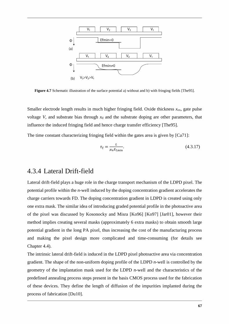
67
Figure 4.7 Schematic illustration of the surface potential a) without and b) with fringing fields [The95].
Smaller electrode length results in much higher fringing field. Oxide thickness xox, gate pulse
voltage V, and substrate bias through xd and the substrate doping are other parameters, that
influence the induced fringing field and hence charge transfer efficiency [The95].
The time constant characterizing fringing field within the gates area is given by [Ca71]:
𝜏f =𝐿
𝜇n𝐸f,min. (4.3.17)
4.3.4 Lateral Drift-field
Lateral drift-field plays a huge role in the charge transport mechanism of the LDPD pixel. The
potential profile within the n-well induced by the doping concentration gradient accelerates the
charge carriers towards FD. The doping concentration gradient in LDPD is created using only
one extra mask. The similar idea of introducing graded potential profile in the photoactive area
of the pixel was discussed by Kosonocky and Misra [Ko96] [Ko97] [Jar01], however their
method implies creating several masks (approximately 6 extra masks) to obtain smooth large
potential gradient in the long PA pixel, thus increasing the cost of the manufacturing process
and making the pixel design more complicated and time-consuming (for details see
Chapter 4.4).
The intrinsic lateral drift-field is induced in the LDPD pixel photoactive area via concentration
gradient. The shape of the non-uniform doping profile of the LDPD n-well is controlled by the
geometry of the implantation mask used for the LDPD n-well and the characteristics of the
predefined annealing process steps present in the basis CMOS process used for the fabrication
of these devices. They define the length of diffusion of the impurities implanted during the
process of fabrication [Du10].
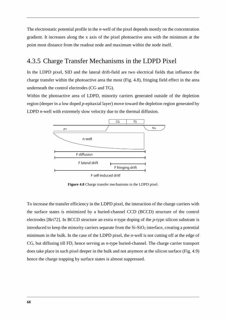
68
The electrostatic potential profile in the n-well of the pixel depends mostly on the concentration
gradient. It increases along the x axis of the pixel photoactive area with the minimum at the
point most distance from the readout node and maximum within the node itself.
4.3.5 Charge Transfer Mechanisms in the LDPD Pixel
In the LDPD pixel, SID and the lateral drift-field are two electrical fields that influence the
charge transfer within the photoactive area the most (Fig. 4.8), fringing field effect in the area
underneath the control electrodes (CG and TG).
Within the photoactive area of LDPD, minority carriers generated outside of the depletion
region (deeper in a low doped p-epitaxial layer) move toward the depletion region generated by
LDPD n-well with extremely slow velocity due to the thermal diffusion.
Figure 4.8 Charge transfer mechanisms in the LDPD pixel.
To increase the transfer efficiency in the LDPD pixel, the interaction of the charge carriers with
the surface states is minimized by a buried-channel CCD (BCCD) structure of the control
electrodes [Bri72]. In BCCD structure an extra n-type doping of the p-type silicon substrate is
introduced to keep the minority carriers separate from the Si-SiO2 interface, creating a potential
minimum in the bulk. In the case of the LDPD pixel, the n-well is not cutting off at the edge of
CG, but diffusing till FD, hence serving as n-type buried-channel. The charge carrier transport
does take place in such pixel deeper in the bulk and not anymore at the silicon surface (Fig. 4.9)
hence the charge trapping by surface states is almost suppressed.

69
Figure 4.9 Charge flow underneath the control gates (VCG =1.75[V], VTG=2[V]).
The fringing field in BCCD structure of the control electrodes is also increasing [The95]. Since
the minimum potential is now far away from the plane of electrodes, the potential under a given
electrode is influenced not only by the potential of that particular electrode, but also by the
potential of the neighbouring one. Therefore, the potential profile has more slope under the
controlling electrode in the case of BCCD compared to the CCD [Ba75] (Fig. 4.10).
Figure 4.10 Fringing field at the Si-SiO2 interface a) at a shallow depth b) deeper c) in the silicon bulk [The95].
In Figure 4.10 (a) fringing field is very close to the Si-SiO2 interface, its minimum value
underneath the gate biased at 5 V is almost zero. At a certain depth of silicon the influence of
the neighboring gates on the electric field underneath the middle gate is at its highest level
(Fig. 4.10 (b)). The minimum fringing field in this case is at its maximum. Deeper in the silicon
the influence of the fields generated by the neighboring gates is decreasing: at these depths the
various gates are equidistant, and the minimum value of the fringing field decreasing.
Fringing field (and the transfer time respectively) strongly depends on the length of the control
electrode gate. A smaller gate length (TG, CG) introduces a larger fringing field and an
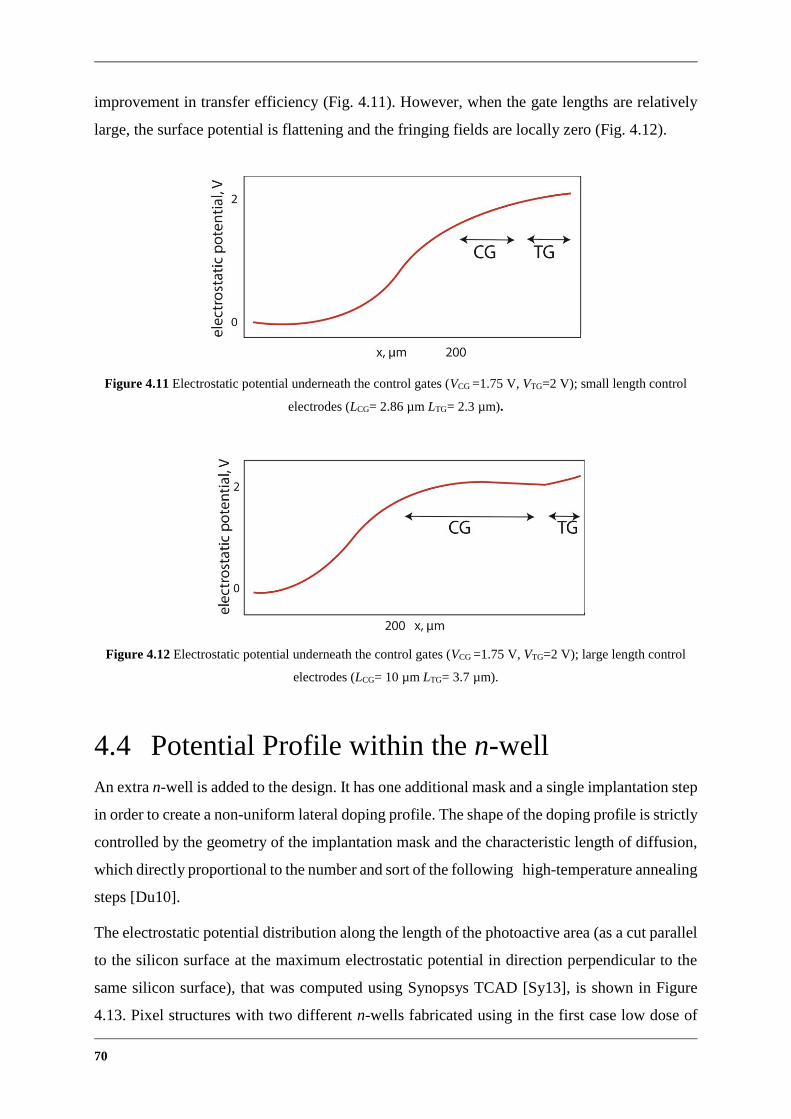
70
improvement in transfer efficiency (Fig. 4.11). However, when the gate lengths are relatively
large, the surface potential is flattening and the fringing fields are locally zero (Fig. 4.12).
Figure 4.11 Electrostatic potential underneath the control gates (VCG =1.75 V, VTG=2 V); small length control
electrodes (LCG= 2.86 µm LTG= 2.3 µm).
Figure 4.12 Electrostatic potential underneath the control gates (VCG =1.75 V, VTG=2 V); large length control
electrodes (LCG= 10 µm LTG= 3.7 µm).
4.4 Potential Profile within the n-well
An extra n-well is added to the design. It has one additional mask and a single implantation step
in order to create a non-uniform lateral doping profile. The shape of the doping profile is strictly
controlled by the geometry of the implantation mask and the characteristic length of diffusion,
which directly proportional to the number and sort of the following high-temperature annealing
steps [Du10].
The electrostatic potential distribution along the length of the photoactive area (as a cut parallel
to the silicon surface at the maximum electrostatic potential in direction perpendicular to the
same silicon surface), that was computed using Synopsys TCAD [Sy13], is shown in Figure
4.13. Pixel structures with two different n-wells fabricated using in the first case low dose of
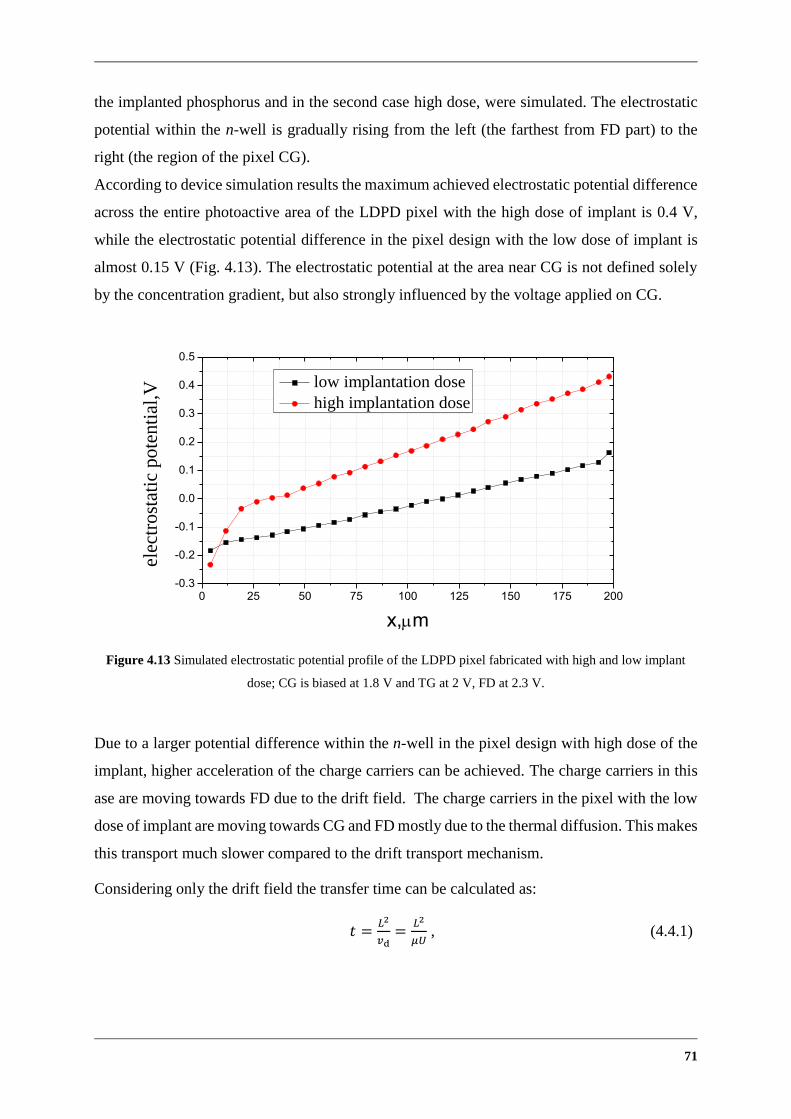
71
the implanted phosphorus and in the second case high dose, were simulated. The electrostatic
potential within the n-well is gradually rising from the left (the farthest from FD part) to the
right (the region of the pixel CG).
According to device simulation results the maximum achieved electrostatic potential difference
across the entire photoactive area of the LDPD pixel with the high dose of implant is 0.4 V,
while the electrostatic potential difference in the pixel design with the low dose of implant is
almost 0.15 V (Fig. 4.13). The electrostatic potential at the area near CG is not defined solely
by the concentration gradient, but also strongly influenced by the voltage applied on CG.
0 25 50 75 100 125 150 175 200-0.3
-0.2
-0.1
0.0
0.1
0.2
0.3
0.4
0.5
elec
tro
stat
ic p
ote
nti
al,V
x,m
low implantation dose
high implantation dose
Figure 4.13 Simulated electrostatic potential profile of the LDPD pixel fabricated with high and low implant
dose; CG is biased at 1.8 V and TG at 2 V, FD at 2.3 V.
Due to a larger potential difference within the n-well in the pixel design with high dose of the
implant, higher acceleration of the charge carriers can be achieved. The charge carriers in this
ase are moving towards FD due to the drift field. The charge carriers in the pixel with the low
dose of implant are moving towards CG and FD mostly due to the thermal diffusion. This makes
this transport much slower compared to the drift transport mechanism.
Considering only the drift field the transfer time can be calculated as:
𝑡 =𝐿2
𝑣d=
𝐿2
𝜇𝑈 , (4.4.1)
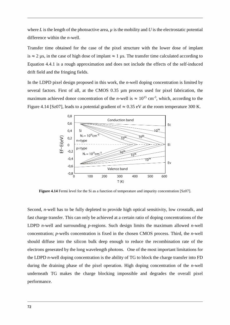
72
where L is the length of the photoactive area, µ is the mobility and U is the electrostatic potential
difference within the n-well.
Transfer time obtained for the case of the pixel structure with the lower dose of implant
is ≈ 2 µs, in the case of high dose of implant ≈ 1 µs. The transfer time calculated according to
Equation 4.4.1 is a rough approximation and does not include the effects of the self-induced
drift field and the fringing fields.
In the LDPD pixel design proposed in this work, the n-well doping concentration is limited by
several factors. First of all, at the CMOS 0.35 µm process used for pixel fabrication, the
maximum achieved donor concentration of the n-well is ≈ 1015 cm-3, which, according to the
Figure 4.14 [Sz07], leads to a potential gradient of ≈ 0.35 eV at the room temperature 300 K.
Figure 4.14 Fermi level for the Si as a function of temperature and impurity concentration [Sz07].
Second, n-well has to be fully depleted to provide high optical sensitivity, low crosstalk, and
fast charge transfer. This can only be achieved at a certain ratio of doping concentrations of the
LDPD n-well and surrounding p-regions. Such design limits the maximum allowed n-well
concentration; p-wells concentration is fixed in the chosen CMOS process. Third, the n-well
should diffuse into the silicon bulk deep enough to reduce the recombination rate of the
electrons generated by the long wavelength photons. One of the most important limitations for
the LDPD n-well doping concentration is the ability of TG to block the charge transfer into FD
during the draining phase of the pixel operation. High doping concentration of the n-well
underneath TG makes the charge blocking impossible and degrades the overall pixel
performance.
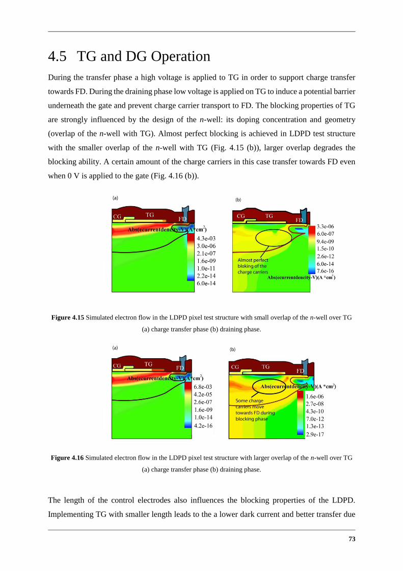
73
4.5 TG and DG Operation
During the transfer phase a high voltage is applied to TG in order to support charge transfer
towards FD. During the draining phase low voltage is applied on TG to induce a potential barrier
underneath the gate and prevent charge carrier transport to FD. The blocking properties of TG
are strongly influenced by the design of the n-well: its doping concentration and geometry
(overlap of the n-well with TG). Almost perfect blocking is achieved in LDPD test structure
with the smaller overlap of the n-well with TG (Fig. 4.15 (b)), larger overlap degrades the
blocking ability. A certain amount of the charge carriers in this case transfer towards FD even
when 0 V is applied to the gate (Fig. 4.16 (b)).
Figure 4.15 Simulated electron flow in the LDPD pixel test structure with small overlap of the n-well over TG
(a) charge transfer phase (b) draining phase.
Figure 4.16 Simulated electron flow in the LDPD pixel test structure with larger overlap of the n-well over TG
(a) charge transfer phase (b) draining phase.
The length of the control electrodes also influences the blocking properties of the LDPD.
Implementing TG with smaller length leads to the a lower dark current and better transfer due

74
to a higher fringing field, but at the same time it lowers the potential barrier induced underneath
TG during the draining phase. Charge carriers then can be transported to FD and disturb the
readout (Fig. 4.17).
Figure 4.17 Simulated electrostatic potential in the LDPD pixel with the smaller length of TG and applied 0V;
the cut was made at the potential maximum depth.
4.6 Crosstalk
Crosstalk is defined as an interaction between neighbouring pixels that could be of optical
nature, when photons get reflected and transmitted through different layers covering the silicon
surface into the neighbouring pixels, or electrical in nature, when photogenerated electrons can
diffuse into neighbouring collection sites contributing to the signals of the neighbouring pixels.
4.6.1 Electrical Crosstalk
Electrical crosstalk is caused by the diffusion of the photogenerated minority carriers into the
neighbouring accumulation sites (neighbouring pixels) [Ag03]. When the incident light strikes
the photoactive area, most of the charge carriers are generated and collected in the potential
well. Charges generated outside of the depletion region either partially recombine and not
contribute to the output signal, or diffuse into the depletion region of the “right” pixel. Or, in
the worst case, they diffuse to the neighbouring pixels (neighbouring potential wells), as it can
be observed in Figure 4.18.

75
Figure 4.18 Schematic view of the electrical crosstalk.
Electrical crosstalk depends on the wavelength of impinging photons, i.e. the depth at which
the electrons get generated within the silicon, and on the diffusion lengths of these electrons.
Long wavelength photons tend to penetrate deeper into the substrate due to the decreasing
absorption coefficient of the silicon that causes the charge carriers to be generated outside of
the depletion region. These photogenerated carriers have a higher probability to diffuse into the
neighbouring potential wells causing electrical crosstalk. Short wavelength photons generate
charges close to the silicon surface. Such charge carriers, generated inside the depletion zone,
are continuously held in the induced electric field, thus they stay in the potential well not
causing any electrical crosstalk.
An increase of the minority carrier diffusion length (caused e.g. by the diminished doping
concentration of the p-type substrate surrounding the pixel n-wells) increases the diffusion
possibility and thus rises the probability for the electrical crosstalk to appear.
4.6.2 Optical Crosstalk
Optical crosstalk results from multiple reflection, refraction, and scattering processes of the
incoming light taking place on different surfaces covering the photoactive silicon substrate,
mainly interfaces between insulators. When the light beam irradiates one pixel, it may also be
deflected to the neighbouring pixels before being absorbed, thus contributing to the
neighbouring pixels output signal. This effect is called optical crosstalk. Optical crosstalk
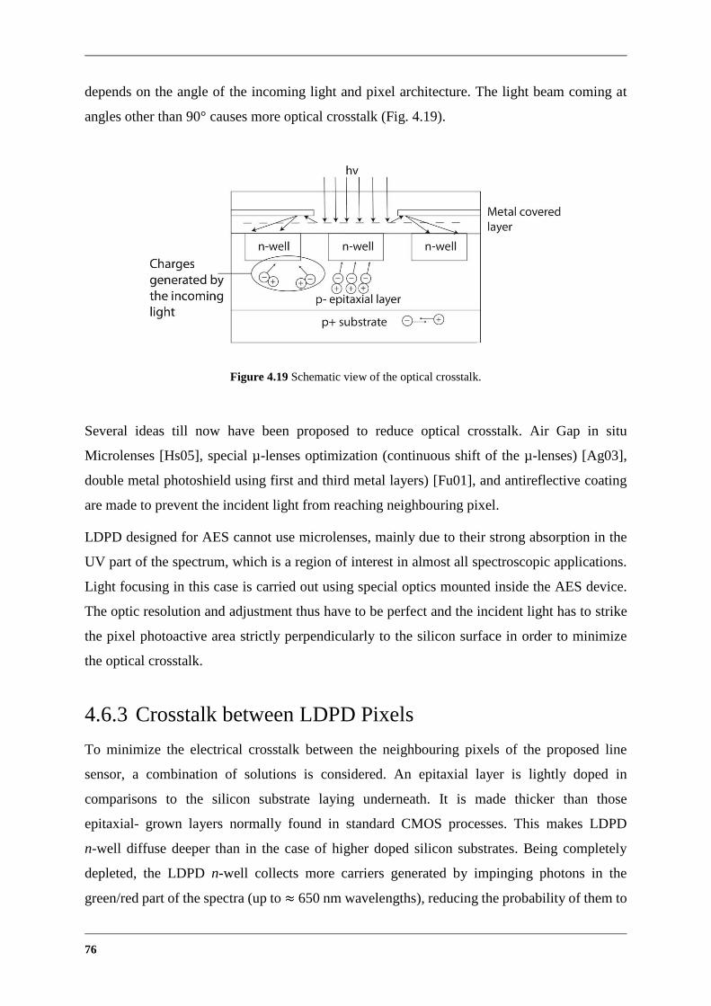
76
depends on the angle of the incoming light and pixel architecture. The light beam coming at
angles other than 90° causes more optical crosstalk (Fig. 4.19).
Figure 4.19 Schematic view of the optical crosstalk.
Several ideas till now have been proposed to reduce optical crosstalk. Air Gap in situ
Microlenses [Hs05], special µ-lenses optimization (continuous shift of the µ-lenses) [Ag03],
double metal photoshield using first and third metal layers) [Fu01], and antireflective coating
are made to prevent the incident light from reaching neighbouring pixel.
LDPD designed for AES cannot use microlenses, mainly due to their strong absorption in the
UV part of the spectrum, which is a region of interest in almost all spectroscopic applications.
Light focusing in this case is carried out using special optics mounted inside the AES device.
The optic resolution and adjustment thus have to be perfect and the incident light has to strike
the pixel photoactive area strictly perpendicularly to the silicon surface in order to minimize
the optical crosstalk.
4.6.3 Crosstalk between LDPD Pixels
To minimize the electrical crosstalk between the neighbouring pixels of the proposed line
sensor, a combination of solutions is considered. An epitaxial layer is lightly doped in
comparisons to the silicon substrate laying underneath. It is made thicker than those
epitaxial- grown layers normally found in standard CMOS processes. This makes LDPD
n-well diffuse deeper than in the case of higher doped silicon substrates. Being completely
depleted, the LDPD n-well collects more carriers generated by impinging photons in the
green/red part of the spectra (up to ≈ 650 nm wavelengths), reducing the probability of them to

77
diffuse into the neighbouring pixels. A trade-off to be met here is related to the maximal depth
of the LDPD n-well that can be reached maintaining its complete depletion of charge carriers
and the width of the non-depleted epitaxial layer beneath it that should be kept at the minimum.
All the carriers generated beneath this region in the highly doped silicon substrate, should be
repelled from the photoactive region of the pixel (due to the potential barrier induced on its
border) to the lower doped epitaxial layer, and eventually recombine causing no contribution to
the electrical crosstalk. On the other hand, such design would negatively affect the spectral
responsivity of the pixels in the NIR part of the spectra- a second trade-off to be considered
during the pixel design.
The second approach to suppress electrical crosstalk is adding deep p-well implantations
between the pixel n-wells. This induces potential barriers and prevents the diffusion of the
minority carriers from the region beneath one n-well into the region of the neighbouring one.
Implanted to both sides of each LDPD n-well, deep p-wells induce potential barriers between
the pixels preventing electrons to diffuse across. To investigate the actual influence of the
introduced p-well, the interface between two photoactive areas of the neighbouring pixels was
simulated in TCAD Synopsys software package [Sy13]. The simulation results of the doping
density between two pixels are presented in Figure 4.20. They confirm perfect separation the
n-wells.
Figure 4.20 2D TCAD simulation of the n-well of the two neighbouring LDPD pixels.
A similar problem arises in the area between TG and DG. However, the simulated electrostatic
potential profile depicted in Figure 4.21 (a) shows that the p-well located between the two
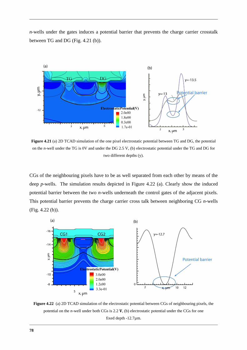
78
n-wells under the gates induces a potential barrier that prevents the charge carrier crosstalk
between TG and DG (Fig. 4.21 (b)).
Figure 4.21 (a) 2D TCAD simulation of the one pixel electrostatic potential between TG and DG, the potential
on the n-well under the TG is 0V and under the DG 2.5 V, (b) electrostatic potential under the TG and DG for
two different depths (y).
CGs of the neighbouring pixels have to be as well separated from each other by means of the
deep p-wells. The simulation results depicted in Figure 4.22 (a). Clearly show the induced
potential barrier between the two n-wells underneath the control gates of the adjacent pixels.
This potential barrier prevents the charge carrier cross talk between neighboring CG n-wells
(Fig. 4.22 (b)).
Figure 4.22 (a) 2D TCAD simulation of the electrostatic potential between CGs of neighbouring pixels, the
potential on the n-well under both CGs is 2.2 𝐕, (b) electrostatic potential under the CGs for one
fixed depth -12.7µm.

79
5 Development of the LDPD-Based Pixel
Pixel development from the LDPD-based photodiode characterization (quantum efficiency and
dark current) to a complete pixel test structure characterization is presented in the current
chapter. The results of the TCAD simulations that were made to better understand and improve
the pixel performance are discussed. Mistakes made during the first design phase and
difficulties are also reviewed in this chapter.
5.1 Goal specification
The CMOS line sensor to be implemented in AES should fulfil the specifications listed in
Table 5.1.
Parameters Units
Goal specification
Min. Typ. Max.
Responsivity (R)
@ tINT
= 60 µs, ER = 3nW/cm²-80000
nW/cm², = 525 nm
V/µJ/cm² 400 430 -
Photo response non uniformity @50% FS
(PRNU) % Not defined
Dark signal non uniformity (DSNU) % - 3 5
Pixel Saturation Capacity (SC) ke 40 45 -
Capacitance Sence Node (CSN
) fF Not defined
Conversion Gain (S) µV/e- 10 12 -
Signal -to -Noise Ratio (SNR) dB 36 39 -
Dynamic Range (DR) dB 45 50 -
Read noise e-rms - 36 -
Transfer time µs - 10 -
Dark Current pA/cm2 - 56
-
Dark Current e-/s - 7000
-
Output signal Linearity
@ = 525nm % 0 0.5 5
Table 5.1 Goal specification.
Ideally, the proposed pixel design should have a large photoactive area to capture as many
incoming photons as possible. Minimum photoactive area needs not to be smaller than
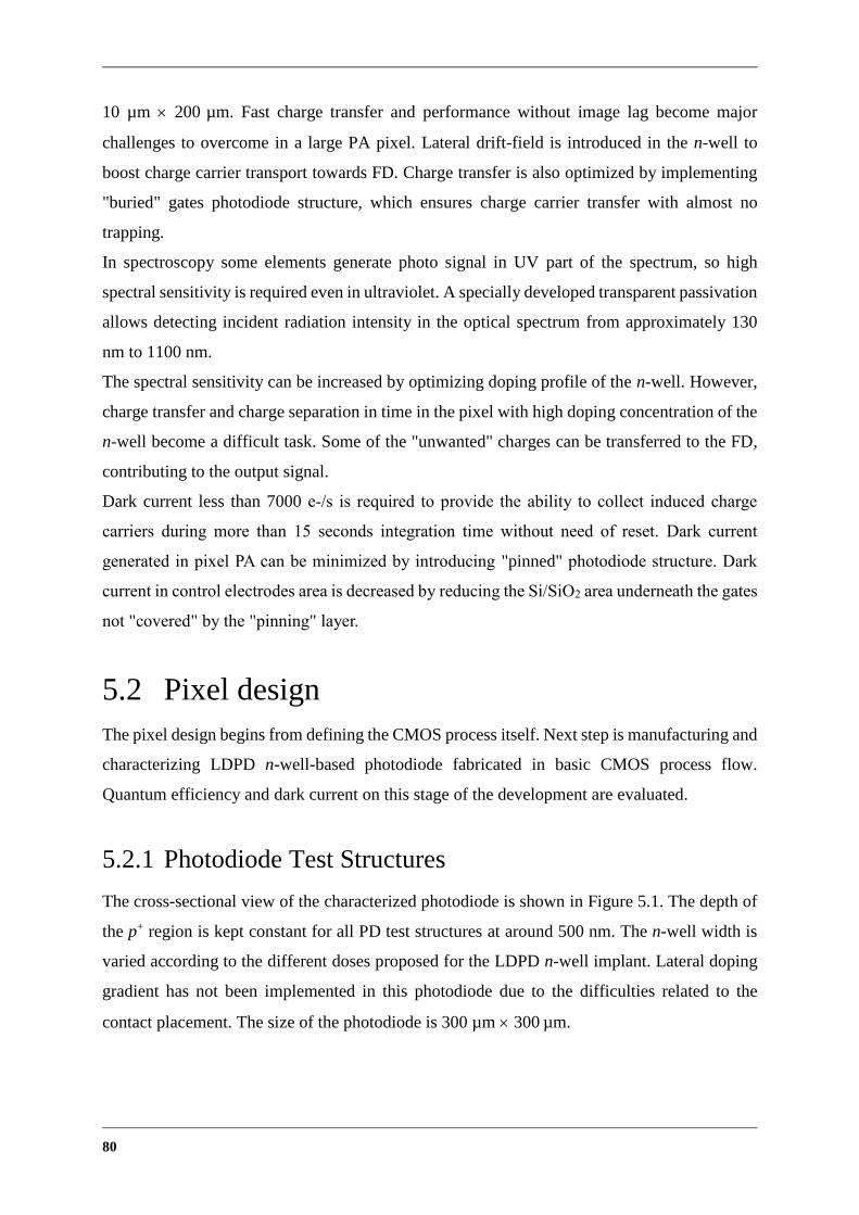
80
10 µm 200 µm. Fast charge transfer and performance without image lag become major
challenges to overcome in a large PA pixel. Lateral drift-field is introduced in the n-well to
boost charge carrier transport towards FD. Charge transfer is also optimized by implementing
"buried" gates photodiode structure, which ensures charge carrier transfer with almost no
trapping.
In spectroscopy some elements generate photo signal in UV part of the spectrum, so high
spectral sensitivity is required even in ultraviolet. A specially developed transparent passivation
allows detecting incident radiation intensity in the optical spectrum from approximately 130
nm to 1100 nm.
The spectral sensitivity can be increased by optimizing doping profile of the n-well. However,
charge transfer and charge separation in time in the pixel with high doping concentration of the
n-well become a difficult task. Some of the "unwanted" charges can be transferred to the FD,
contributing to the output signal.
Dark current less than 7000 e-/s is required to provide the ability to collect induced charge
carriers during more than 15 seconds integration time without need of reset. Dark current
generated in pixel PA can be minimized by introducing "pinned" photodiode structure. Dark
current in control electrodes area is decreased by reducing the Si/SiO2 area underneath the gates
not "covered" by the "pinning" layer.
5.2 Pixel design
The pixel design begins from defining the CMOS process itself. Next step is manufacturing and
characterizing LDPD n-well-based photodiode fabricated in basic CMOS process flow.
Quantum efficiency and dark current on this stage of the development are evaluated.
5.2.1 Photodiode Test Structures
The cross-sectional view of the characterized photodiode is shown in Figure 5.1. The depth of
the p+ region is kept constant for all PD test structures at around 500 nm. The n-well width is
varied according to the different doses proposed for the LDPD n-well implant. Lateral doping
gradient has not been implemented in this photodiode due to the difficulties related to the
contact placement. The size of the photodiode is 300 µm 300 µm.
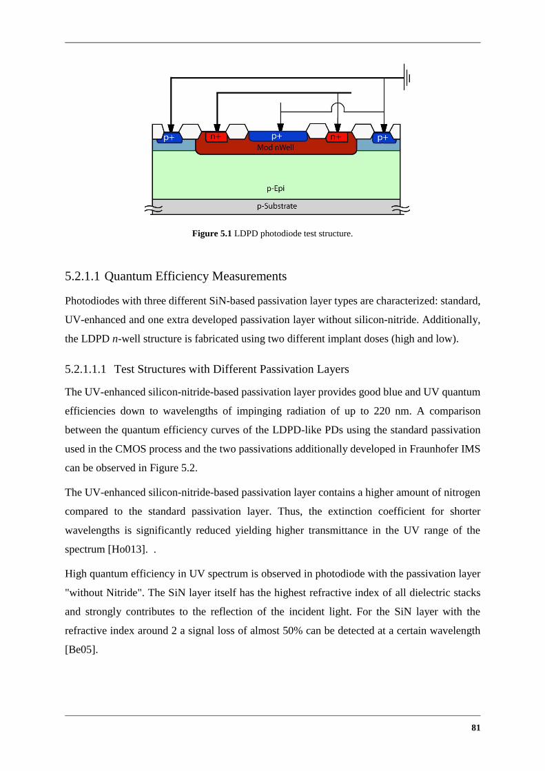
81
Figure 5.1 LDPD photodiode test structure.
5.2.1.1 Quantum Efficiency Measurements
Photodiodes with three different SiN-based passivation layer types are characterized: standard,
UV-enhanced and one extra developed passivation layer without silicon-nitride. Additionally,
the LDPD n-well structure is fabricated using two different implant doses (high and low).
5.2.1.1.1 Test Structures with Different Passivation Layers
The UV-enhanced silicon-nitride-based passivation layer provides good blue and UV quantum
efficiencies down to wavelengths of impinging radiation of up to 220 nm. A comparison
between the quantum efficiency curves of the LDPD-like PDs using the standard passivation
used in the CMOS process and the two passivations additionally developed in Fraunhofer IMS
can be observed in Figure 5.2.
The UV-enhanced silicon-nitride-based passivation layer contains a higher amount of nitrogen
compared to the standard passivation layer. Thus, the extinction coefficient for shorter
wavelengths is significantly reduced yielding higher transmittance in the UV range of the
spectrum [Ho013]. .
High quantum efficiency in UV spectrum is observed in photodiode with the passivation layer
"without Nitride". The SiN layer itself has the highest refractive index of all dielectric stacks
and strongly contributes to the reflection of the incident light. For the SiN layer with the
refractive index around 2 a signal loss of almost 50% can be detected at a certain wavelength
[Be05].

82
200 250 300 350 400 450-0.1
0.0
0.1
0.2
0.3
0.4
0.5
0.6
0.7
QE
wavelength,nm
standart passivation
passivation without Nitride
UV enhanced passivation
Figure 5.2 Quantum efficiency vs wavelength curves obtained from the LDPD test structures using three
different passivation layers.
5.2.1.1.2 Test Structures with Different LDPD n-well Implantations
Figure 5.3 shows the change of the quantum efficiency in LDPD-like PDs for two different
doses of the n-well implant. The quantum efficiency of the PD with the higher dose of implant
is higher in 400 nm - 800 nm wavelength range. Lower quantum efficiency is largely due to the
absorption of the long wavelength photons that happens not in the depletion zone but in the
p-epitaxial layer, and the recombination losses related to this process.
The n-wells of the PDs fabricated with low dose of implant do not diffuse deeper in the silicon
bulk. The depletion zone in this case is very narrow. The collected number of electrons
generated from the longer wavelength photons in the PD with narrow depletion zone is much
lower than in the case of PD with wider space charge region. It is important to note that beneath
the p-type epitaxial layer there is a highly doped silicon substrate. All the electrons
photogenerated in this region will immediately recombine as there is a potential barrier induced
at the interface between the highly doped substrate and the lower doped epitaxial layer that
pushes them back into the highly doped silicon bulk. During the fabrication process there is a

83
diffusion of boron atoms from the highly doped substrate into the epitaxial layer that reduces
the thickness of the neutral epitaxial layer beneath the LDPD n-well. Due to fixed and
well-defined annealing steps in the CMOS process flow, the thickness of this region does not
change, which makes it directly dependent only on the out-diffusion of the n-well itself.
As it can be observed in Figure 5.3, for the short wavelength photons (up to 400 nm) striking
the pixel photoactive area roughly the same number of charge carriers is collected for test
structures with both doses of implant.
0 200 400 600 800 1000 12000.0
0.2
0.4
0.6
0.8
QE
wavelength,nm
6*1011 cm-2, UV-transp.passiv
3*1011 cm-2, UV-transp.passiv
Figure 5.3 Quantum efficiency vs wavelength curves obtained from the LDPD test structures with two different
dose of the n-well implant.
5.2.1.2 I/V Characteristics
The dark current was measured on the LDPD-like PD in order to determine the contribution of
the area and perimeter dark currents generated in the photoactive area of the pixel to the total
dark current of the pixel and to determine which of these components has stronger influence on
the overall dark current generated in the PA.
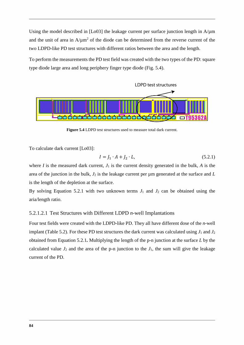
84
Using the model described in [Lo03] the leakage current per surface junction length in A/µm
and the unit of area in A/µm2 of the diode can be determined from the reverse current of the
two LDPD-like PD test structures with different ratios between the area and the length.
To perform the measurements the PD test field was created with the two types of the PD: square
type diode large area and long periphery finger type diode (Fig. 5.4).
Figure 5.4 LDPD test structures used to measure total dark current.
To calculate dark current [Lo03]:
𝐼 = 𝐽1 ∙ 𝐴 + 𝐽2 ∙ 𝐿, (5.2.1)
where I is the measured dark current, J1 is the current density generated in the bulk, A is the
area of the junction in the bulk, J2 is the leakage current per µm generated at the surface and L
is the length of the depletion at the surface.
By solving Equation 5.2.1 with two unknown terms J1 and J2 can be obtained using the
aria/length ratio.
5.2.1.2.1 Test Structures with Different LDPD n-well Implantations
Four test fields were created with the LDPD-like PD. They all have different dose of the n-well
implant (Table 5.2). For these PD test structures the dark current was calculated using J1 and J2
obtained from Equation 5.2.1. Multiplying the length of the p-n junction at the surface L by the
calculated value J2 and the area of the p-n junction to the J1, the sum will give the leakage
current of the PD.

85
Test chip n-well Implantation Dose
cm-2, Energy kEv Passivation
Test chip A 2.8 1011, 350 Standard
Test chip B 4. 1011, 350 Standard
Test chip C 6 1011, 350 Standard
Test chip D 8 1011, 350 Standard
Table 5.2 PD test structures.
In the Table 5.3 the dark current density J1 and J2 can be obtained for the LDPD pixel with the
area 200 10 µm2 is shown for four different PDs. The dark current is increasing proportionally
to the depletion-layer width, which in turn depends on the junction doping profile
(see Chapter 4).
Narrowing the depletion region is one solution to reduce the depletion dark current, which is a
side effect reduces quantum efficiency quit significantly (almost 50%) and hence the spectral
sensitivity of the LDPD pixel.
Test chip Dark Current Density
pA/cm2
Test chip A 11
Test chip B 20
Test chip C 27
Test chip D 95
Table 5.3 Calculated dark current.
Calculated dark current of the LDPD test structures vs the dose of the implant n-well is shown
on Figure 5.5. Total dark current generated on LDPD test structures includes depletion dark
current and diffusion dark current. The depletion dark current according to the theory (see
Chapter 4) is proportional to the width of the depletion region. The width of the depletion region
is in turn proportional to the implantation dose of the n-well: the higher the implantation dose
is the wider the n-well and depletion zone are. Therefore, it can be assumed, that the depletion
dark current is directly proportional to the implantation dose of the n-well. This dependence
can be seen in Figure 5.5.

86
2 3 4 5 6 7 80
20
40
60
80
100
Dar
k c
urr
ent,
pA
/cm
2
n-well implantation dose*E11,cm-3
Figure 5.5 Dark current on LDPD test structures vs the dose of the implant n-well.
5.2.1.2.2 Temperature Dependence
P+ implantation implemented in the PD test structures suppresses the dark current generated
by the interface traps located on the surface of the PD. Therefore, the surface component of the
area-dependent dark current that commonly dominates in the overall PD dark current is in this
case almost negligible.
The mechanisms of the dark current can be investigated using its temperature dependence graph
shown in Figure 5.6. The activation energy at low temperatures below 40 ºC for the area
component of the dark current is around Eg/2 (0.56 eV), and at higher temperatures it is around
Eg (1.12 eV). This means that for the area-dependent component, the recombination-generation
mechanism of the dark current dominate at low temperatures and the diffusion mechanism
dominates at higher temperatures.
For the perimeter component of the dark current the activation energy is close to Eg/2 even at
higher temperatures. In this case thermal generation of electrons is due to the interface traps
caused by defective sidewalls and edges.

87
Figure 5.6 Area and perimeter-dependent components of the dark current generated in the PDs extracted from
the measurements of the test structures.
5.3 Electrical parameters
The electrical parameters of the proposed LDPD pixel can be approximately calculated using
the measurement results obtained from the PD test structures and the specification given at the
Chapter 5.
5.3.1 Output Voltage Swing
Following readout concept was described in detail in the Chapter 3.5 (see also Fig. 5.7). The
FD voltage swing can be defined as:
∆𝑉FD =𝑛∙𝑞
𝐶SN. (5.3.1)
The pixel output swing then can be calculated as:
∆𝑉out = 𝐴Vtotal ∙ ∆𝑉FD = 𝐴Vtotal ∙𝑛∙𝑞
𝐶SN (5.3.2)
Gain of the SF transistor has been simulated using "Cadence" simulation software
as: 𝐴VSF= 𝐴Vbuffer = 0.75, then:
𝐴Vtotal= 𝐴VSF
∙ 𝐴Vbuffer = 0.56, (5.3.3)
∆𝑉out max = ∆𝑉FDmax ∙ 𝐴Vtotal.

88
For ∆𝑉FDmax = 3.3 𝑉 (in the case of PMOS transistor as a RST and depletion NMOS transistor
as SF)
∆𝑉out max = 1.8 𝑉. (5.3.4)
Figure 5.7 Readout concept of the proposed LDPD pixel.
5.3.2 Floating Diffusion Capacitance
Considering the CSN = CFD + parasitic capacitance (parasitic capacitance of the SF-gate
electrode, etc.) Equation 5.3.4, ∆𝑉FDmax = 3.3 𝑉 and taking into account Equation 5.3.2 the
sense node capacitance is calculated as:
𝐶SN = 𝐴Vtotal∙
𝑛∙𝑞
∆𝑉out max= 7.2 𝑓𝐹. (5.3.5)
The parasitic capacitance is estimated via "Cadence" simulation software of 4 fF,
𝐶FD = 3.2 𝑓𝐹.
To determine the area of FD n+ diffusion the surface- and area-dependent capacitances of the
n+-diffusion has been measured. The model to define the total capacitance is similar to the one
described above (Chapter 5.2).
The total capacitance can be obtained as:
𝐶 = 𝐶A ∙ 𝐴 + 𝐶P ∙ 𝑃, (5.3.6)
where Ca and Cp are the area - and perimeter - dependent components of the capacitance,
respectively A and P are the area and the perimeter of the test PD.
The area of FD can then be calculated taking into account estimated values of
𝐶A = 38 𝑛𝐹/𝑐𝑚2, 𝐶P = 1.65 𝑝𝐹/𝑐𝑚, 𝐶FD = 3.2 𝑓𝐹 as:
𝐴FD = 4.84 × 10⁻⁸ 𝑐𝑚2. (5.3.7)

89
5.3.3 Spectral Responsivity
The spectral responsivity is calculated according to the Equation 4.3.1. Considering OS (optical
sensitivity) equal to 0.4 A/W at the λ = 660 nm, that was obtained from the quantum efficiency
measurement (see Chapter 5.2), we get:
𝑅 = 𝑂𝑆 ∙ 𝐴ph ∙𝐴SF
𝐶SN= 640
𝑉∙𝑐𝑚2
𝜇𝐽. (5.3.8)
The estimated spectral responsivity is higher than specified (Table 5.1), but the optical
sensitivity value used in the calculation was obtained for the PD test structures fabricated using
the standard n-well mask, OS for the LDPD pixel with the non-uniformal lateral doping profile
of an extra n-well is lower due to the smaller overall width of the depletion zone, so the "real"
responsivity value is expected to be lower.
5.3.4 Noise and Dynamic Range
The dark noise can be calculated according to the specification (see Chapter 5.1) for the pixel
with saturation capacity of FWC = 45000 e- and the dark current 7000 e-:
𝐸𝑁𝐶dark = √𝑛dark = √7000 = 84 𝑒− 𝑟𝑚𝑠, (5.3.9)
the photon noise is defined as:
𝐸𝑁𝐶ph = √𝑛ph = √𝑛FWC − 𝑛dark = 195 𝑒− 𝑟𝑚𝑠. (5.3.10)
The read out noise is specified to be:
𝐸𝑁𝐶read = 36 𝑒− 𝑟𝑚𝑠. (5.3.11)
The total noise then is calculated as:
𝐸𝑁𝐶total dark = √𝐸𝑁𝐶dark2 + 𝐸𝑁𝐶read
2 = 92 𝑒− 𝑟𝑚𝑠. (5.3.12)
Dynamic range is estimated as:
𝐷𝑅 = 20 ∙ 𝑙𝑜𝑔𝑛ph
𝐸𝑁𝐶total dark= 52 𝑑𝐵. (5.3.13)
And maximum signal-to-noise ratio is defined as:
𝑆𝑁𝑅max = 20 ∙ 𝑙𝑜𝑔𝑛ph
√𝐸𝑁𝐶dark2 +𝐸𝑁𝐶ph
2 +𝐸𝑁𝐶read2
= 44 𝑑𝐵. (5.3.14)
For the enhanced PMOS as a RST-transistor and a depletion NMOS transistor as SF, reset
noise for the 𝐶SN = 7.2 𝑓𝐹 is:
𝐸𝑁𝐶RST =1
𝑞√𝑘𝑇𝐶SN = 34 𝑒−𝑟𝑚𝑠. (5.3.15)
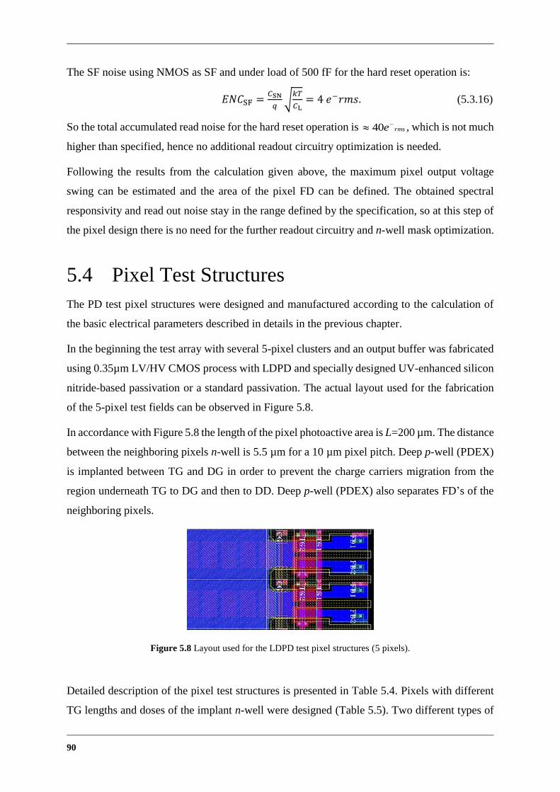
90
The SF noise using NMOS as SF and under load of 500 fF for the hard reset operation is:
𝐸𝑁𝐶SF =𝐶SN
𝑞√
𝑘𝑇
𝐶L= 4 𝑒−𝑟𝑚𝑠. (5.3.16)
So the total accumulated read noise for the hard reset operation is , which is not much
higher than specified, hence no additional readout circuitry optimization is needed.
Following the results from the calculation given above, the maximum pixel output voltage
swing can be estimated and the area of the pixel FD can be defined. The obtained spectral
responsivity and read out noise stay in the range defined by the specification, so at this step of
the pixel design there is no need for the further readout circuitry and n-well mask optimization.
5.4 Pixel Test Structures
The PD test pixel structures were designed and manufactured according to the calculation of
the basic electrical parameters described in details in the previous chapter.
In the beginning the test array with several 5-pixel clusters and an output buffer was fabricated
using 0.35µm LV/HV CMOS process with LDPD and specially designed UV-enhanced silicon
nitride-based passivation or a standard passivation. The actual layout used for the fabrication
of the 5-pixel test fields can be observed in Figure 5.8.
In accordance with Figure 5.8 the length of the pixel photoactive area is L=200 µm. The distance
between the neighboring pixels n-well is 5.5 µm for a 10 µm pixel pitch. Deep p-well (PDEX)
is implanted between TG and DG in order to prevent the charge carriers migration from the
region underneath TG to DG and then to DD. Deep p-well (PDEX) also separates FD’s of the
neighboring pixels.
Figure 5.8 Layout used for the LDPD test pixel structures (5 pixels).
Detailed description of the pixel test structures is presented in Table 5.4. Pixels with different
TG lengths and doses of the implant n-well were designed (Table 5.5). Two different types of
rmse 40
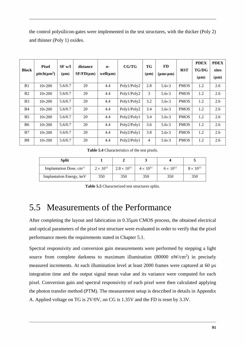
91
the control polysilicon-gates were implemented in the test structures, with the thicker (Poly 2)
and thinner (Poly 1) oxides.
Block Pixel
pitch(μm2)
SF w/l
(μm)
distance
SF/FD(μm)
n-
well(μm)
CG/TG
TG
(μm)
FD
(μmμm) RST
PDEX
TG/DG
(μm)
PDEX
sites
(μm)
B1 10200 5.6/0.7 20 4.4 Poly1/Poly2 2.8 5.63 PMOS 1.2 2.6
B2 10200 5.6/0.7 20 4.4 Poly1/Poly2 3 5.63 PMOS 1.2 2.6
B3 10200 5.6/0.7 20 4.4 Poly1/Poly2 3.2 5.63 PMOS 1.2 2.6
B4 10200 5.6/0.7 20 4.4 Poly1/Poly2 3.4 5.63 PMOS 1.2 2.6
B5 10200 5.6/0.7 20 4.4 Poly2/Poly1 3.4 5.63 PMOS 1.2 2.6
B6 10200 5.6/0.7 20 4.4 Poly2/Poly1 3.6 5.63 PMOS 1.2 2.6
B7 10200 5.6/0.7 20 4.4 Poly2/Poly1 3.8 5.63 PMOS 1.2 2.6
B8 10200 5.6/0.7 20 4.4 Poly2/Poly1 4 5.63 PMOS 1.2 2.6
Table 5.4 Characteristics of the test pixels.
Split 1 2 3 4 5
Implantation Dose, cm-2 2 1011 2.8 1011 4 1011 6 1011 8 1011
Implantation Energy, keV 350 350 350 350 350
Table 5.5 Characterized test structures splits.
5.5 Measurements of the Performance
After completing the layout and fabrication in 0.35µm CMOS process, the obtained electrical
and optical parameters of the pixel test structure were evaluated in order to verify that the pixel
performance meets the requirements stated in Chapter 5.1.
Spectral responsivity and conversion gain measurements were performed by stepping a light
source from complete darkness to maximum illumination (80000 nW/cm2) in precisely
measured increments. At each illumination level at least 2000 frames were captured at 60 µs
integration time and the output signal mean value and its variance were computed for each
pixel. Conversion gain and spectral responsivity of each pixel were then calculated applying
the photon transfer method (PTM). The measurement setup is described in details in Appendix
A. Applied voltage on TG is 2V/0V, on CG is 1.35V and the FD is reset by 3.3V.

92
Spectral responsivity, dark current, transfer time, and conversion gain are major parameters that
were evaluated to analyze pixel performance and obtain information needed for the further
LDPD pixel optimization.
5.5.1 Responsivity and Quantum Efficiency
The best in terms of the achieved performance is the test pixel B7 with the higher dose of
implant, length of TG 3.8 µm and the following gates structure: CG built with the thicker oxide
(Poly 2), TG with the thinner oxide (Poly 1). The responsivity of this pixel is measured to be
170 V/µJ/cm2 at the wavelenght of impinging radiation λ =525 nm and conversion gain
is 6.7 µV/e- (Table 5.6)
When test pixel structure CG is implemented with the thinner oxide, and TG with the thicker
oxide, the electrostatic potential in the initial period underneath CG is becoming higher or equal
to the one underneath TG (2 V is applied on TG and 1.75 V on CG). During the charge transfer,
the electrostatic potential underneath TG/FD decreases and the possibility for the charge
carriers to be transferred from CG area to FD decreases as well. The charge carriers in this case
are "stuck" underneath CG and do not move towards FD. The spectral responsivity dramatically
decreases compared to test pixel structures with TG built on thinner oxide and CG built on
thicker one.
Parameter Units Goal
Specification
Results
obtained with
the low
implant dose
Results
obtained with
the high
implant dose
Conversion gain μV/e 12 7.08 6.7
Responsivity
(λ = 525 nm, Tint = 60 μs) V/(μJ/cm2) 430 170 270
Table 5.6 Measurement results of the test pixel structures.
The obtained conversion gain and spectral responsivity are too low for the AES application, so
further optimization of the LDPD pixel needs to be done. To increase the conversion gain, the
floating diffusion capacitance should be dramatically reduced. Following dependence in
Equation 5.1.1 the area of the sense node should then be decreased:
𝐶𝐺 =160∙2∙10−15
𝐶FD, [
𝜇𝑉
𝑒−]. (5.5.1)
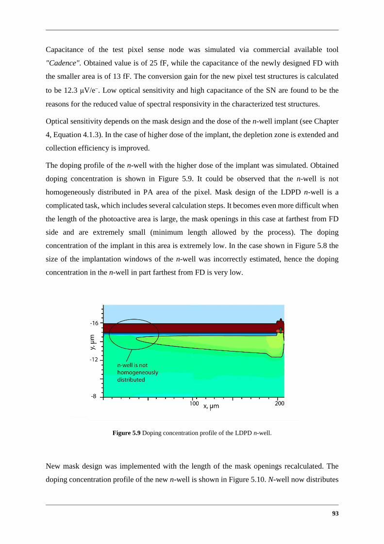
93
Capacitance of the test pixel sense node was simulated via commercial available tool
"Cadence". Obtained value is of 25 fF, while the capacitance of the newly designed FD with
the smaller area is of 13 fF. The conversion gain for the new pixel test structures is calculated
to be 12.3 μV/e. Low optical sensitivity and high capacitance of the SN are found to be the
reasons for the reduced value of spectral responsivity in the characterized test structures.
Optical sensitivity depends on the mask design and the dose of the n-well implant (see Chapter
4, Equation 4.1.3). In the case of higher dose of the implant, the depletion zone is extended and
collection efficiency is improved.
The doping profile of the n-well with the higher dose of the implant was simulated. Obtained
doping concentration is shown in Figure 5.9. It could be observed that the n-well is not
homogeneously distributed in PA area of the pixel. Mask design of the LDPD n-well is a
complicated task, which includes several calculation steps. It becomes even more difficult when
the length of the photoactive area is large, the mask openings in this case at farthest from FD
side and are extremely small (minimum length allowed by the process). The doping
concentration of the implant in this area is extremely low. In the case shown in Figure 5.8 the
size of the implantation windows of the n-well was incorrectly estimated, hence the doping
concentration in the n-well in part farthest from FD is very low.
Figure 5.9 Doping concentration profile of the LDPD n-well.
New mask design was implemented with the length of the mask openings recalculated. The
doping concentration profile of the new n-well is shown in Figure 5.10. N-well now distributes

94
homogeneously over the photoactive area of the pixel, hence the increase of the optical sensitive
can be expected.
Figure 5.10 Doping concentration profile of the redesigned LDPD n-well.
Another way to increase optical sensitivity is the extension of the mask openings widths
(Fig. 5.11). The crosstalk in the designed pixel is suppressed (see Chapter 4) by implementing
deep p-well between the n-wells of the neighbouring pixels. Pixel pitch is defined by the
specification to be 10 µm and the width of the n-well openings in the characterized pixel design
is chosen to be 4.4 µm to maximize the distance between two pixel n-wells.
Figure 5.11 Layout of the initial and redesigned LDPD n-well.
In the redesigned pixel the width of the n-well openings is 5.6 µm (1.2 µm larger compared to
the previous design). This change is supposed to increase the optical sensitivity by increasing
the n-well area and at the same time not to multiply the electrical crosstalk due to a smaller
separation between the neighbouring pixels.

95
To test the neighbouring n-wells separation, TCAD simulation of the two pixels with the
redesigned n-wells were performed. The doping concentration profile of the two adjusted
n-wells is demonstrated in Figure 5.12. It can be clearly seen that the n-wells are perfectly
separated. The potential barrier between two neighbouring n-wells is supposed to decrease in
comparison to the simulated potential barrier of the previous n-well design presented in
Chapter 4.
Figure 5.12 Doping concentration profile of the two neighbouring pixel n-wells.
The doping concentration profile of the n-well with the low dose of the implant and no overlap
of the n-well with TG is shown in Figure 5.13 (TG/FD part of the pixel). Small p-well is
separating n-well and FD, which leads to the charge transfer problem and causes decrease of
the spectral responsivity. Charge carriers in this case are transferred from the photodiode area
to the floating diffusion and can come in contact with the Si-SiO2 surface in the region near FD
and interact with the surface traps. Charge trapping and detrapping might occur.
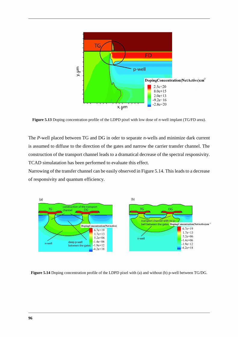
96
Figure 5.13 Doping concentration profile of the LDPD pixel with low dose of n-well implant (TG/FD area).
The P-well placed between TG and DG in oder to separate n-wells and minimize dark current
is assumed to diffuse to the direction of the gates and narrow the carrier transfer channel. The
construction of the transport channel leads to a dramatical decrease of the spectral responsivity.
TCAD simulatation has been performed to evaluate this effect.
Narrowing of the transfer channel can be easily observed in Figure 5.14. This leads to a decrease
of responsivity and quantum efficiency.
Figure 5.14 Doping concentration profile of the LDPD pixel with (a) and without (b) p-well between TG/DG.
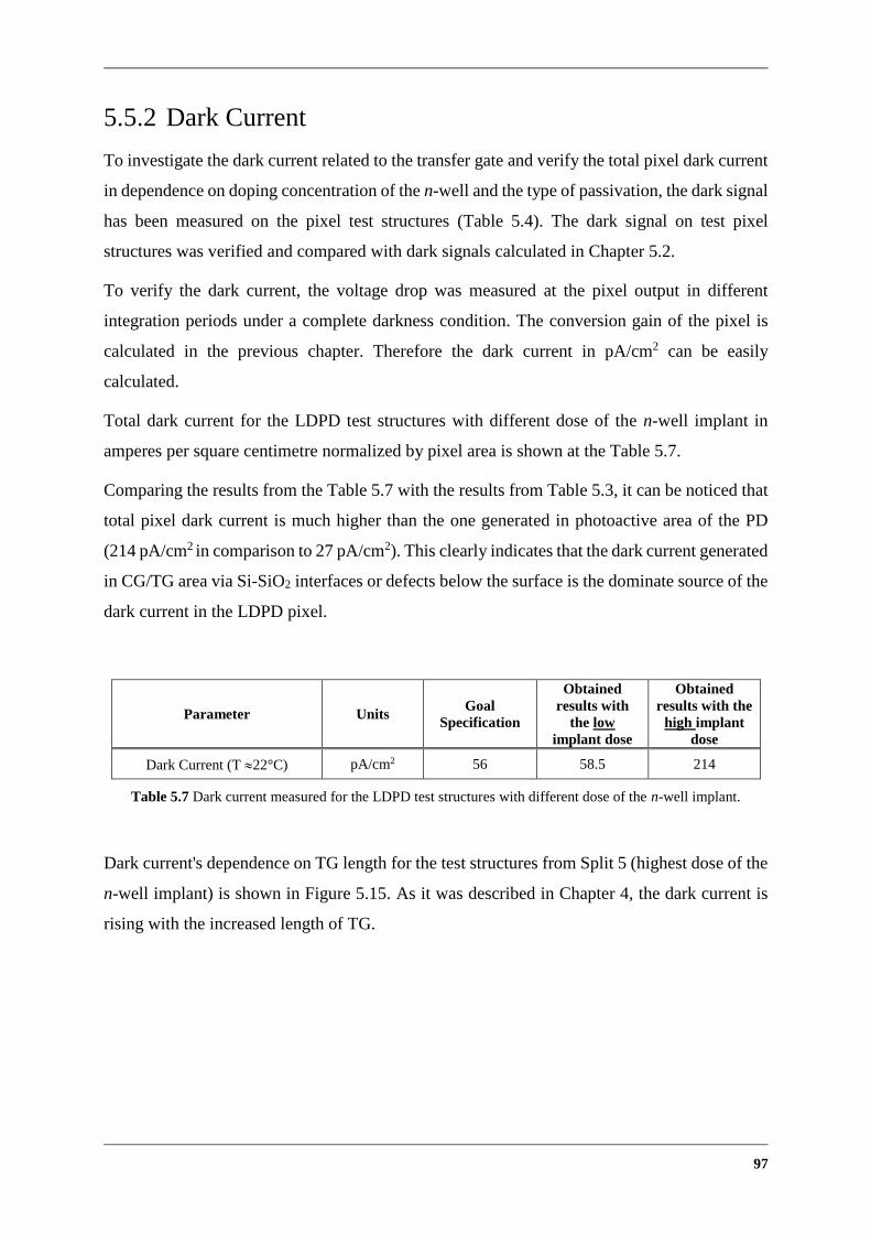
97
5.5.2 Dark Current
To investigate the dark current related to the transfer gate and verify the total pixel dark current
in dependence on doping concentration of the n-well and the type of passivation, the dark signal
has been measured on the pixel test structures (Table 5.4). The dark signal on test pixel
structures was verified and compared with dark signals calculated in Chapter 5.2.
To verify the dark current, the voltage drop was measured at the pixel output in different
integration periods under a complete darkness condition. The conversion gain of the pixel is
calculated in the previous chapter. Therefore the dark current in pA/cm2 can be easily
calculated.
Total dark current for the LDPD test structures with different dose of the n-well implant in
amperes per square centimetre normalized by pixel area is shown at the Table 5.7.
Comparing the results from the Table 5.7 with the results from Table 5.3, it can be noticed that
total pixel dark current is much higher than the one generated in photoactive area of the PD
(214 pA/cm2 in comparison to 27 pA/cm2). This clearly indicates that the dark current generated
in CG/TG area via Si-SiO2 interfaces or defects below the surface is the dominate source of the
dark current in the LDPD pixel.
Parameter Units Goal
Specification
Obtained
results with
the low
implant dose
Obtained
results with the
high implant
dose
Dark Current (T 22°C) pA/cm2 56 58.5 214
Table 5.7 Dark current measured for the LDPD test structures with different dose of the n-well implant.
Dark current's dependence on TG length for the test structures from Split 5 (highest dose of the
n-well implant) is shown in Figure 5.15. As it was described in Chapter 4, the dark current is
rising with the increased length of TG.
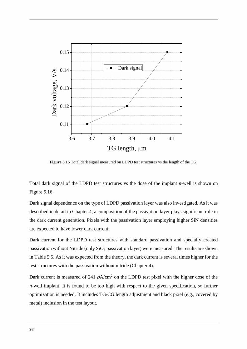
98
3.6 3.7 3.8 3.9 4.0 4.1
0.11
0.12
0.13
0.14
0.15
Dar
k v
olt
age,
V/s
TG length, m
Dark signal
Figure 5.15 Total dark signal measured on LDPD test structures vs the length of the TG.
Total dark signal of the LDPD test structures vs the dose of the implant n-well is shown on
Figure 5.16.
Dark signal dependence on the type of LDPD passivation layer was also investigated. As it was
described in detail in Chapter 4, a composition of the passivation layer plays significant role in
the dark current generation. Pixels with the passivation layer employing higher SiN densities
are expected to have lower dark current.
Dark current for the LDPD test structures with standard passivation and specially created
passivation without Nitride (only SiO2 passivation layer) were measured. The results are shown
in Table 5.5. As it was expected from the theory, the dark current is several times higher for the
test structures with the passivation without nitride (Chapter 4).
Dark current is measured of 241 A/cm2 on the LDPD test pixel with the higher dose of the
n-well implant. It is found to be too high with respect to the given specification, so further
optimization is needed. It includes TG/CG length adjustment and black pixel (e.g., covered by
metal) inclusion in the test layout.

99
2 3 4 5 6 7 8 9
0.04
0.06
0.08
0.10
0.12
0.14
Dar
k v
olt
age,
V/s
n-well implantation dose*E11, cm
Dark signal
Figure 5.16 Total dark signal measured on LDPD test structures vs the dose of the implant n-well.
The black ("dummy") pixels prevent the diffusion of the dark electrons generated outside of the
pixel array to the n-wells or FDs of the active pixel and increasing the total pixel dark current.
The new 5-pixel test structure is shown schematically in Figure 5.17.
Figure 5.17 New 5-pixel test structure with two "dummy" pixels located on both sides of the test cluster.
5.5.3 Transfer Time
LDPD is designed to reduce image lag by decreasing the charge transfer time. Specially
designed lateral graded-doping profile enhances the lateral electric field and speeds up the
signal charge transfer from PA to FD.
A potential within the pixel photoactive area is determined by the mask design of the n-well
and the dose of n-well implant. The higher the dose, the higher is the doping concentration
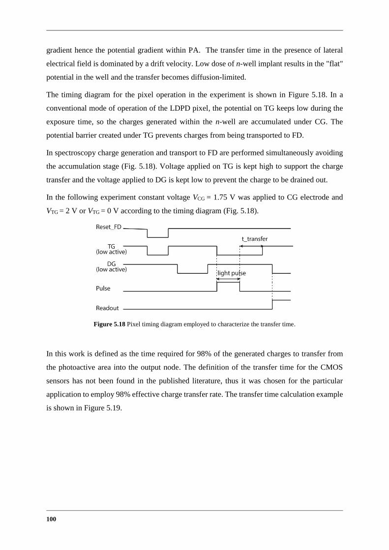
100
gradient hence the potential gradient within PA. The transfer time in the presence of lateral
electrical field is dominated by a drift velocity. Low dose of n-well implant results in the "flat"
potential in the well and the transfer becomes diffusion-limited.
The timing diagram for the pixel operation in the experiment is shown in Figure 5.18. In a
conventional mode of operation of the LDPD pixel, the potential on TG keeps low during the
exposure time, so the charges generated within the n-well are accumulated under CG. The
potential barrier created under TG prevents charges from being transported to FD.
In spectroscopy charge generation and transport to FD are performed simultaneously avoiding
the accumulation stage (Fig. 5.18). Voltage applied on TG is kept high to support the charge
transfer and the voltage applied to DG is kept low to prevent the charge to be drained out.
In the following experiment constant voltage VCG = 1.75 V was applied to CG electrode and
VTG = 2 V or VTG = 0 V according to the timing diagram (Fig. 5.18).
Figure 5.18 Pixel timing diagram employed to characterize the transfer time.
In this work is defined as the time required for 98% of the generated charges to transfer from
the photoactive area into the output node. The definition of the transfer time for the CMOS
sensors has not been found in the published literature, thus it was chosen for the particular
application to employ 98% effective charge transfer rate. The transfer time calculation example
is shown in Figure 5.19.
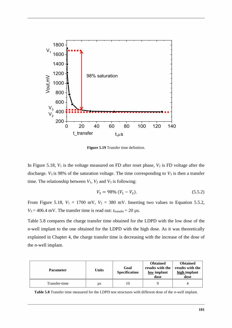
101
Figure 5.19 Transfer time definition.
In Figure 5.18, V1 is the voltage measured on FD after reset phase, V2 is FD voltage after the
discharge. V3 is 98% of the saturation voltage. The time corresponding to V3 is then a transfer
time. The relationship between V1, V2 and V3 is following:
𝑉3 = 98% (𝑉1 − 𝑉2). (5.5.2)
From Figure 5.18, V1 = 1700 mV, V2 = 380 mV. Inserting two values to Equation 5.5.2,
V3 = 406.4 mV. The transfer time is read out: ttransfer = 20 µs.
Table 5.8 compares the charge transfer time obtained for the LDPD with the low dose of the
n-well implant to the one obtained for the LDPD with the high dose. As it was theoretically
explained in Chapter 4, the charge transfer time is decreasing with the increase of the dose of
the n-well implant.
Parameter Units Goal
Specification
Obtained
results with the
low implant
dose
Obtained
results with the
high implant
dose
Transfer-time µs 10 9 4
Table 5.8 Transfer time measured for the LDPD test structures with different dose of the n-well implant.
0 20 40 60 80 100 120 140200
400
600
800
1000
1200
1400
1600
1800
Vo
ut,
mV
t,st_transfer
98% saturation
V1
V2
V3
102
Charge transfer time is measured for the LDPD test structure with the higher dose of n-well
implant to be 4 µs. It fully satisfies the goal from specification, so further optimization for the
particular application is not needed.
5.5.4 LDPD Test Pixel Optimization
Performance parameters of the characterized LDPD test structures are summarized in
Table 5.9.
Parameter Units Goal
Specification
Obtained
results with
the low
implant dose
Obtained
results with
the high
implant dose
Conversion gain μV/e 12 7.08 6.7
Responsivity
(λ = 525 nm, Tint = 80 μs) V/(μJ/cm2) 430 170 270
Dark Current (T 22°C) pA/cm2 56 59 214
Transfer Time µs 10 9 4
Table 5.9 Measurement results of the LDPD test structures.
The maximum spectral responsivity is measured 270 V/(μJ/cm2) and the conversion gain to be
7 μV/e . These values are too low for the AES application. Dark current of 214 pA/cm2 is too
high, thus new LDPD test structures with the same pixel pitch organized via the same principle
of having 19 different 7-pixel clusters are proposed.
A new n-well mask design and higher dose of the n-well implant together with the several times
decreased area of FD proposed to increase the spectral responsivity and conversion gain. Deep
p-well that separates TG and DG should be also optimized in order to maximize optical
sensitivity and improve charge transfer.
The dark current can be decreased by introducing "dummy" pixels at the both sides of the
5-pixel cluster and by changing the geometry of TG/CG and FD.
The transfer time is a major concern during the development of a CMOS line sensor due to the
extra-long PA that introduces difficulties in the collection and transport of the charge carriers.
Increase of the electrostatic potential gradient (implementing higher dose of the n-well implant)
and correctly biased CG and TG make the transfer of the charge carriers fast and efficient.

103
Transfer time for the LDPD test structure was measured to be 5-10 µs and is expected to be fast
enough for many applications.
Charge transfer can still be improved by increasing the overlap of the n-well with TG, thereby
minimizing charge trapping and detrapping at the Si-SiO2 interface near FD.

104
6 Experimental results Design of the LDPD pixel for AES CMOS line sensor is presented in this chapter. All major
design steps are listed and discussed. The measured pixel parameter values are compared to the
theoretical assessments and simulation results presented in the previous chapter.
Performance analysis of the LDPD pixel includes dark current and transfer time
characterization, crosstalk observation, spectral responsivity measurements, and evaluation of
the pixel quantum efficiency. The influence of the geometry such as length of the collection
gate and transfer gate on pixel performance is discussed. Dark current and crosstalk are
considered. Effective solutions to leakage current minimization and electrical crosstalk
suppression are presented.
Basic performance of the pixel with new n-well mask design, proposed in the previous chapter,
is evaluated. Such n-well is expected to increase optical sensitivity and quantum efficiency of
the pixel and at the same time avoid introducing additional crosstalk and dark current.
Dependence of the overlap of the n-well with TG on the spectral responsivity is discussed. An
assumption about the p-well, designed to prevent crosstalk between the n-wells underneath TG
and DG narrowing the transfer channel and thereby worsening the charge transport, is
investigated. A special attention is paid to the transfer time characterization, since transfer time
is of one the main concerns during the LDPD pixel design. Pixel with completely new n-well
mask design is proposed. Its theoretical performance is evaluated via TCAD Synopsys. New
pixel design is that optimizes charge transfer in the LDPD n-well is created.
Pixel with the best performance parameters is selected. 1×368 CMOS line sensor is
manufactured using the pixel with the best characteristics. Basic parameters of this sensor are
measured (see Chapter 7).
6.1 Basic Characterization using the
Photon-Transfer Method (PTM)
Performance parameters of the LDPD pixel such as spectral responsivity and quantum
efficiency were evaluated. The setup described in the Appendix A was used to measure both
parameters. Calculation was performed based on the PTM (see Appendix C).
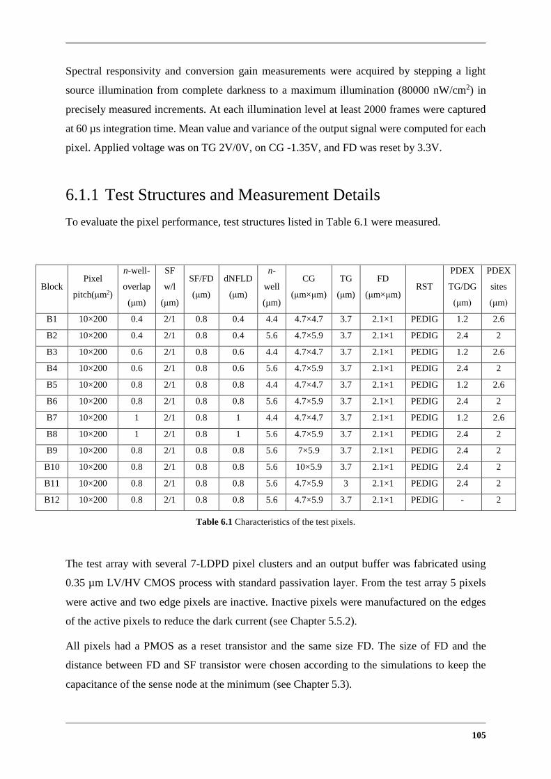
105
Spectral responsivity and conversion gain measurements were acquired by stepping a light
source illumination from complete darkness to a maximum illumination (80000 nW/cm2) in
precisely measured increments. At each illumination level at least 2000 frames were captured
at 60 µs integration time. Mean value and variance of the output signal were computed for each
pixel. Applied voltage was on TG 2V/0V, on CG -1.35V, and FD was reset by 3.3V.
6.1.1 Test Structures and Measurement Details
To evaluate the pixel performance, test structures listed in Table 6.1 were measured.
Block Pixel
pitch(μm2)
n-well-
overlap
(μm)
SF
w/l
(μm)
SF/FD
(μm)
dNFLD
(μm)
n-
well
(μm)
CG
(μm×μm)
TG
(μm)
FD
(μm×μm) RST
PDEX
TG/DG
(μm)
PDEX
sites
(μm)
B1 10×200 0.4 2/1 0.8 0.4 4.4 4.7×4.7 3.7 2.1×1 PEDIG 1.2 2.6
B2 10×200 0.4 2/1 0.8 0.4 5.6 4.7×5.9 3.7 2.1×1 PEDIG 2.4 2
B3 10×200 0.6 2/1 0.8 0.6 4.4 4.7×4.7 3.7 2.1×1 PEDIG 1.2 2.6
B4 10×200 0.6 2/1 0.8 0.6 5.6 4.7×5.9 3.7 2.1×1 PEDIG 2.4 2
B5 10×200 0.8 2/1 0.8 0.8 4.4 4.7×4.7 3.7 2.1×1 PEDIG 1.2 2.6
B6 10×200 0.8 2/1 0.8 0.8 5.6 4.7×5.9 3.7 2.1×1 PEDIG 2.4 2
B7 10×200 1 2/1 0.8 1 4.4 4.7×4.7 3.7 2.1×1 PEDIG 1.2 2.6
B8 10×200 1 2/1 0.8 1 5.6 4.7×5.9 3.7 2.1×1 PEDIG 2.4 2
B9 10×200 0.8 2/1 0.8 0.8 5.6 7×5.9 3.7 2.1×1 PEDIG 2.4 2
B10 10×200 0.8 2/1 0.8 0.8 5.6 10×5.9 3.7 2.1×1 PEDIG 2.4 2
B11 10×200 0.8 2/1 0.8 0.8 5.6 4.7×5.9 3 2.1×1 PEDIG 2.4 2
B12 10×200 0.8 2/1 0.8 0.8 5.6 4.7×5.9 3.7 2.1×1 PEDIG - 2
Table 6.1 Characteristics of the test pixels.
The test array with several 7-LDPD pixel clusters and an output buffer was fabricated using
0.35 µm LV/HV CMOS process with standard passivation layer. From the test array 5 pixels
were active and two edge pixels are inactive. Inactive pixels were manufactured on the edges
of the active pixels to reduce the dark current (see Chapter 5.5.2).
All pixels had a PMOS as a reset transistor and the same size FD. The size of FD and the
distance between FD and SF transistor were chosen according to the simulations to keep the
capacitance of the sense node at the minimum (see Chapter 5.3).
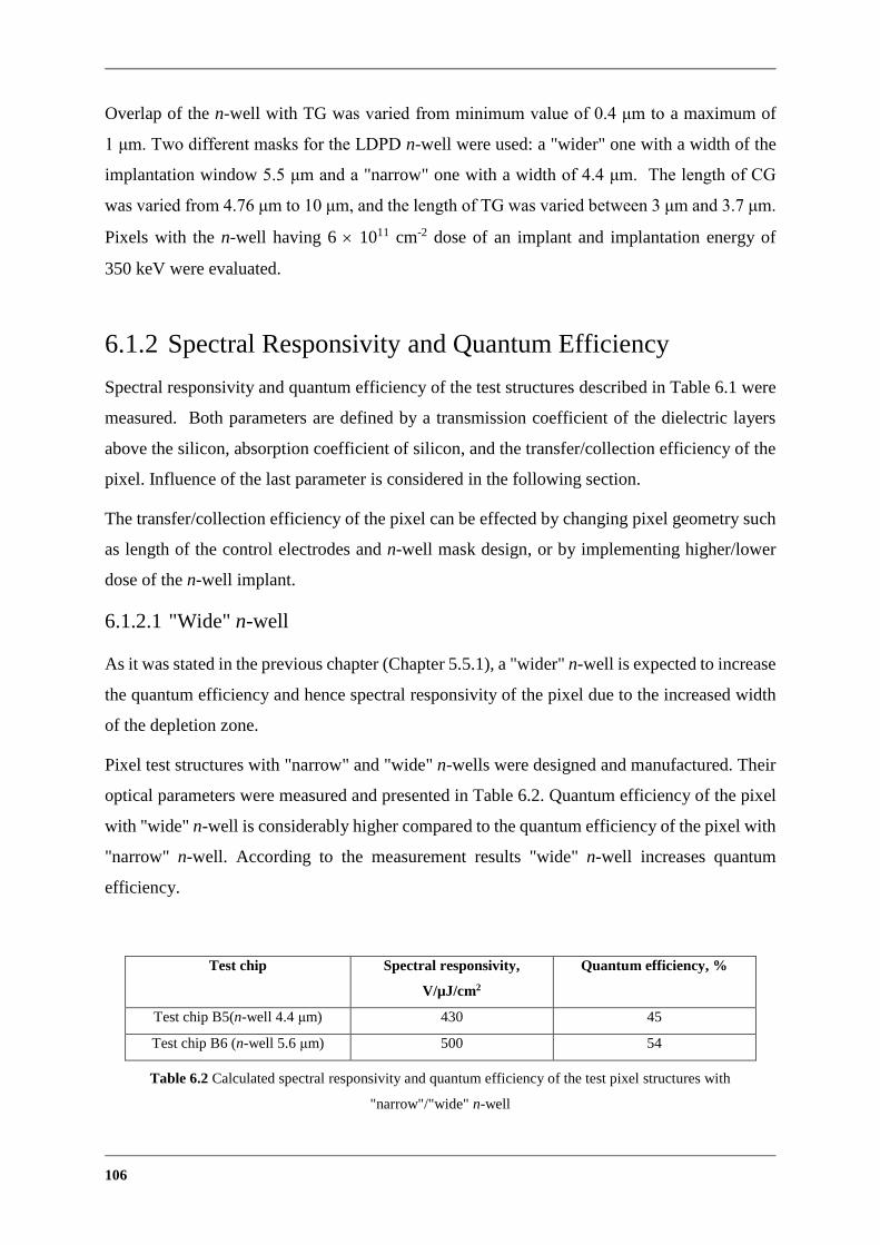
106
Overlap of the n-well with TG was varied from minimum value of 0.4 μm to a maximum of
1 μm. Two different masks for the LDPD n-well were used: a "wider" one with a width of the
implantation window 5.5 μm and a "narrow" one with a width of 4.4 μm. The length of CG
was varied from 4.76 μm to 10 μm, and the length of TG was varied between 3 μm and 3.7 μm.
Pixels with the n-well having 6 1011 cm-2 dose of an implant and implantation energy of
350 keV were evaluated.
6.1.2 Spectral Responsivity and Quantum Efficiency
Spectral responsivity and quantum efficiency of the test structures described in Table 6.1 were
measured. Both parameters are defined by a transmission coefficient of the dielectric layers
above the silicon, absorption coefficient of silicon, and the transfer/collection efficiency of the
pixel. Influence of the last parameter is considered in the following section.
The transfer/collection efficiency of the pixel can be effected by changing pixel geometry such
as length of the control electrodes and n-well mask design, or by implementing higher/lower
dose of the n-well implant.
6.1.2.1 "Wide" n-well
As it was stated in the previous chapter (Chapter 5.5.1), a "wider" n-well is expected to increase
the quantum efficiency and hence spectral responsivity of the pixel due to the increased width
of the depletion zone.
Pixel test structures with "narrow" and "wide" n-wells were designed and manufactured. Their
optical parameters were measured and presented in Table 6.2. Quantum efficiency of the pixel
with "wide" n-well is considerably higher compared to the quantum efficiency of the pixel with
"narrow" n-well. According to the measurement results "wide" n-well increases quantum
efficiency.
Test chip Spectral responsivity,
V/µJ/cm2
Quantum efficiency, %
Test chip B5(n-well 4.4 μm) 430 45
Test chip B6 (n-well 5.6 μm) 500 54
Table 6.2 Calculated spectral responsivity and quantum efficiency of the test pixel structures with
"narrow"/"wide" n-well
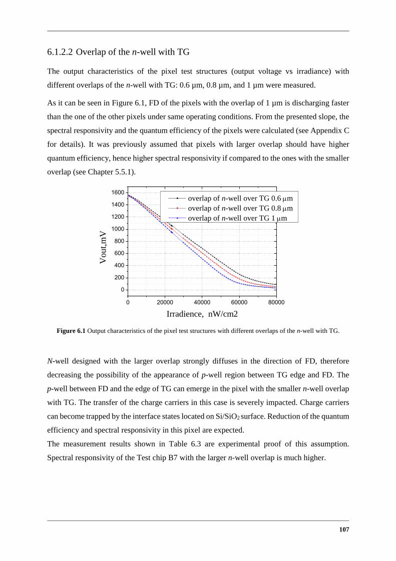
107
6.1.2.2 Overlap of the n-well with TG
The output characteristics of the pixel test structures (output voltage vs irradiance) with
different overlaps of the n-well with TG: 0.6 µm, 0.8 µm, and 1 µm were measured.
As it can be seen in Figure 6.1, FD of the pixels with the overlap of 1 µm is discharging faster
than the one of the other pixels under same operating conditions. From the presented slope, the
spectral responsivity and the quantum efficiency of the pixels were calculated (see Appendix C
for details). It was previously assumed that pixels with larger overlap should have higher
quantum efficiency, hence higher spectral responsivity if compared to the ones with the smaller
overlap (see Chapter 5.5.1).
Figure 6.1 Output characteristics of the pixel test structures with different overlaps of the n-well with TG.
N-well designed with the larger overlap strongly diffuses in the direction of FD, therefore
decreasing the possibility of the appearance of p-well region between TG edge and FD. The
p-well between FD and the edge of TG can emerge in the pixel with the smaller n-well overlap
with TG. The transfer of the charge carriers in this case is severely impacted. Charge carriers
can become trapped by the interface states located on Si/SiO2 surface. Reduction of the quantum
efficiency and spectral responsivity in this pixel are expected.
The measurement results shown in Table 6.3 are experimental proof of this assumption.
Spectral responsivity of the Test chip B7 with the larger n-well overlap is much higher.
0 20000 40000 60000 80000
0
200
400
600
800
1000
1200
1400
1600
Vou
t,m
V
Irradience, nW/cm2
overlap of n-well over TG 0.6m
overlap of n-well over TG 0.8m
overlap of n-well over TG 1m
108
Test chip Spectral responsivity,
V/µJ/cm2
Quantum efficiency,
%
Test chip B3 (overlap n-well 0.6μm) 416 40
Test chip B5 (overlap n-well 0.8μm) 430 45
Test chip B7 (overlap n-well 1 μm) 500 50
Table 6.3 Calculated spectral responsivity and quantum efficiency of the test pixel structures with different
overlaps of n-well with TG.
6.1.2.3 P-well between the Gates
As it was hypothesized in Chapter 5.5.1, p-well between TG and DG can lead to the appearance
of constriction of the transfer channel and, as a consequence, to a decrease of spectral
responsivity and quantum efficiency. Two pixel structures were measured to support this
assumption: first one with the p-well and the second one without.
From the measurement results presented in the Table 6.4 it can be seen that pixel test structure
without p-well has lower quantum efficiency and hence lower spectral responsivity. From these
measurement results we can draw a conclusion: p-well located between TG and DG does
influence charge transfer and it improves it rather that worsening.
The p-well between TG and DG induces high potential barrier that prevents the electrical
crosstalk. It is not any more favourable for the charge carriers to move from TG side to DG. In
the case of the pixel without p-well very low potential barrier between TG and DG lets the
charge carriers move from TG to DG side and then be drained to the higher potential DD. This
process explains both lower quantum efficiency and spectral responsivity for the pixels without
p-well.
Test chip Spectral responsivity,
V/µJ/cm2
Quantum efficiency,
%
Test chip B6 (with p-well) 500 54
Test chip B12 (without p-well) 400 42
Table 6.4 Calculated spectral responsivity and quantum efficiency of the test pixel structures with and without
p-well between TG and DG.
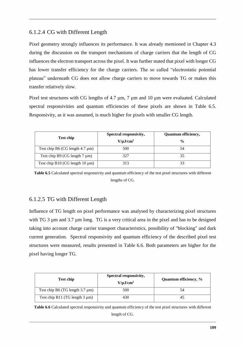
109
6.1.2.4 CG with Different Length
Pixel geometry strongly influences its performance. It was already mentioned in Chapter 4.3
during the discussion on the transport mechanisms of charge carriers that the length of CG
influences the electron transport across the pixel. It was further stated that pixel with longer CG
has lower transfer efficiency for the charge carriers. The so called “electrostatic potential
plateau” underneath CG does not allow charge carriers to move towards TG or makes this
transfer relatively slow.
Pixel test structures with CG lengths of 4.7 µm, 7 µm and 10 µm were evaluated. Calculated
spectral responsivities and quantum efficiencies of these pixels are shown in Table 6.5.
Responsivity, as it was assumed, is much higher for pixels with smaller CG length.
Test chip Spectral responsivity,
V/µJ/cm2
Quantum efficiency,
%
Test chip B6 (CG length 4.7 µm) 500 54
Test chip B9 (CG length 7 µm) 327 35
Test chip B10 (CG length 10 µm) 313 33
Table 6.5 Calculated spectral responsivity and quantum efficiency of the test pixel structures with different
lengths of CG.
6.1.2.5 TG with Different Length
Influence of TG length on pixel performance was analysed by characterizing pixel structures
with TG 3 µm and 3.7 µm long. TG is a very critical area in the pixel and has to be designed
taking into account charge carrier transport characteristics, possibility of "blocking" and dark
current generation. Spectral responsivity and quantum efficiency of the described pixel test
structures were measured, results presented in Table 6.6. Both parameters are higher for the
pixel having longer TG.
Test chip Spectral responsivity,
V/µJ/cm2 Quantum efficiency, %
Test chip B6 (TG length 3.7 µm) 500 54
Test chip B11 (TG length 3 µm) 430 45
Table 6.6 Calculated spectral responsivity and quantum efficiency of the test pixel structures with different
length of CG.
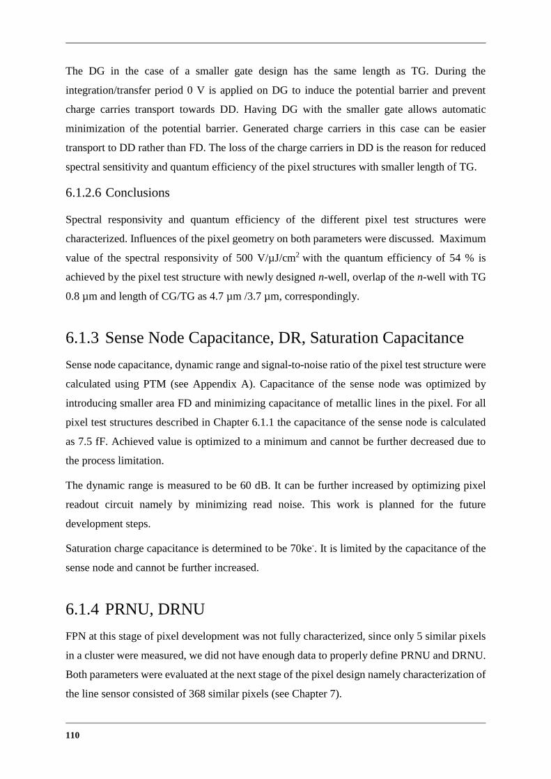
110
The DG in the case of a smaller gate design has the same length as TG. During the
integration/transfer period 0 V is applied on DG to induce the potential barrier and prevent
charge carries transport towards DD. Having DG with the smaller gate allows automatic
minimization of the potential barrier. Generated charge carriers in this case can be easier
transport to DD rather than FD. The loss of the charge carriers in DD is the reason for reduced
spectral sensitivity and quantum efficiency of the pixel structures with smaller length of TG.
6.1.2.6 Conclusions
Spectral responsivity and quantum efficiency of the different pixel test structures were
characterized. Influences of the pixel geometry on both parameters were discussed. Maximum
value of the spectral responsivity of 500 V/µJ/cm2 with the quantum efficiency of 54 % is
achieved by the pixel test structure with newly designed n-well, overlap of the n-well with TG
0.8 µm and length of CG/TG as 4.7 µm /3.7 µm, correspondingly.
6.1.3 Sense Node Capacitance, DR, Saturation Capacitance
Sense node capacitance, dynamic range and signal-to-noise ratio of the pixel test structure were
calculated using PTM (see Appendix A). Capacitance of the sense node was optimized by
introducing smaller area FD and minimizing capacitance of metallic lines in the pixel. For all
pixel test structures described in Chapter 6.1.1 the capacitance of the sense node is calculated
as 7.5 fF. Achieved value is optimized to a minimum and cannot be further decreased due to
the process limitation.
The dynamic range is measured to be 60 dB. It can be further increased by optimizing pixel
readout circuit namely by minimizing read noise. This work is planned for the future
development steps.
Saturation charge capacitance is determined to be 70ke-. It is limited by the capacitance of the
sense node and cannot be further increased.
6.1.4 PRNU, DRNU
FPN at this stage of pixel development was not fully characterized, since only 5 similar pixels
in a cluster were measured, we did not have enough data to properly define PRNU and DRNU.
Both parameters were evaluated at the next stage of the pixel design namely characterization of
the line sensor consisted of 368 similar pixels (see Chapter 7).
111
6.2 Dark Current Characterization
In the standard PD bulk and surface defects are the main sources of the dark current. The
p+- region on the surface of the LDPD suppresses the dark current generated from the surface
defects in the photoactive area. The dark current generated from the surface defects in the
control electrodes area is the major remaining contributor to the total dark current and can be
suppressed by changing for example CG/TG geometry.
Dark current, generated from the interface defects located in the sidewall of the FOX region, is
the primary contributor to the perimeter component of the dark current in the LDPD pixel.
Separating the depletion region of the PD from the FOX region with the p-well as reported in
[Ha06] dramatically reduces the dark current. In the proposed LDPD pixel p-well separated
depletion region and FOX are used. Additional p-well should be introduced in FD area to
separate FD and FOX. That could be implemented in the future designs. Bulk dark current can
be minimized by optimizing CMOS process itself. Bulk dark current optimization is not
considered in this work.
Dark current characterization and optimization of the PD and pixel test structures were
presented in Chapter 5. In this chapter the measurement of the dark current in the LDPD pixel
is described, dependence of the dark current on the geometry of control electrodes and the pixel
layout is shown. Dark current temperature dependence is reviewed.
6.2.1 The Test Structure and Measurement Methodology
An LDPD test array with several 5-pixel test clusters and an output buffer was fabricated in
order to evaluate the dark current using the 0.35 µm CMOS process. The length of the pixel
photoactive area L =200 µm with a 10 µm pixel pitch, the length of CG varies from 4.7 µm to
10 µm, the length of TG varies from 3.7 µm to 2 µm. Phosphor was implanted to create the
n-well with the implantation dose 6 1011 cm-2 and energy 350 keV (see Table 6.7).
The dark signal in the proposed LDPD pixel structures was measured using the test setup
described in details in Appendix B. The potential on CG in all experiments is 1.35 V and on
TG is 2 V. The floating diffusion is reset with 3.3 V.
To evaluate the dark current, the voltage drop at the pixel output is measured during different
integration periods. Knowing the conversion gain, the dark current can be calculated (see

112
Appendix B2 for details). All the dark current measurements were taken at the room
temperature. Statistically averaged data obtained from the three chips measured are presented.
Test chip
Pixel
pitch,
(µm2)
n-well
Implantation Dose
(cm-2), Energy kEv
CG,
(µm)
TG,
(µm)
n-well
overlap over
the TG,(µm)
Passivation Additional
features
Test chip A 10 200 6 1011, 350 4.7 3.7 0.8 Standard
Test chip B 10 200 6 1011, 350 7 3.7 0.8 Standard
Test chip C 10 200 6 1011, 350 10 3.7 0.8 Standard
Test chip D 10 200 5 1011, 350 4.7 3.7 0.8 Standard
Test chip E 10 200 5 1011, 350 4.7 3 0.8 Standard
Test chip F 10 200 5 1011, 350 4.7 2.3 0.8 Standard
Test chip G 10 2 5 1011, 350 4.7 3.7 0.8 Standard 10 2 µm2 PA of
the pixel
Test chip H 10 200 5 1011, 350 4.7 2.3 0.6 Standard
Test chip I 10 200 5 1011, 350 4.7 2.3 1 Standard
Test chip J 10 200 5 1011, 350 4.7 2.3 0.8 Standard
Test chip K 10 200 5 1011, 350 4.7 2.3 0.8 Standard no p-well between
TG and DG
Table 6.7 Varied characteristics of the test chips.
6.2.2 Dark Current versus CG Geometry
To investigate the dark current related to CG area, the dark signal was measured in the LDPD
pixel structures with three different length of the collection gate (test chips A, B and C). Output
characteristics of the pixel test structures are shown on Figure 6.2.
From the data in Figure 6.2 and Table 6.8 it can be noticed that generated dark current is much
higher in the LDPD with longer CG.
Test chip CG length, µm Dark current, e-/s
Test chip A 4.7 4700
Test chip B 7 5300
Test chip C 10 5900
Table 6.8 Calculated dark current of the LDPD test structures with different lengths of CG.

113
The dark current generated by the Shockley-Read-Hall recombination/generation centers
located on the silicon surface under CG depends on the length of the collection gate and can
only be minimized (for LDPD) by changing the CG geometry.
0 2 4 6 8 10 12 14 16
0
200
400
600
800
1000
1200
1400
1600
V,m
V
time,s
CG=4.7m
CG=7m
CG=10m
Figure 6.2 Dark signal of the LDPD test structures with different length of the CG.
6.2.3 Dark Current versus TG Geometry
The same investigation was performed to identify the influence of TG length on the dark current
generated in the pixel. Dark signal of the two test structures with the different lengths of TG
were analysed. From the measurement results (Table 6.9) it follows, that the dark signal
decreases with the decreasing length of TG.
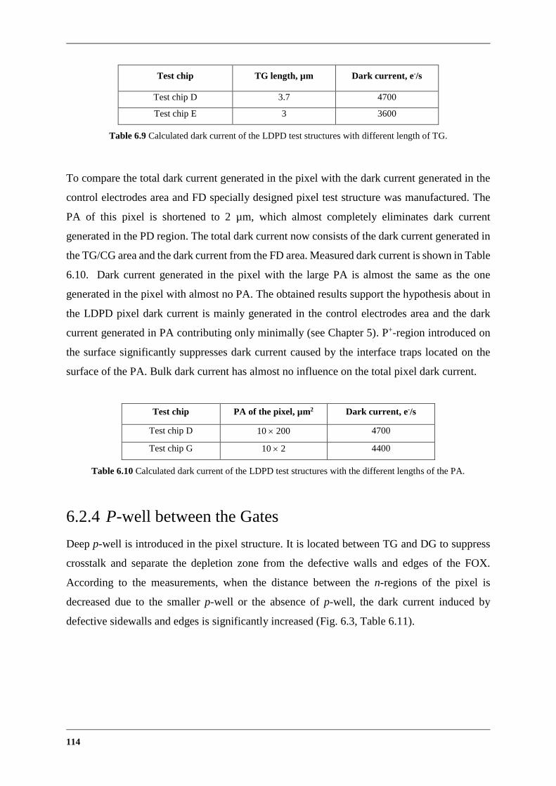
114
Test chip TG length, µm Dark current, e-/s
Test chip D 3.7 4700
Test chip E 3 3600
Table 6.9 Calculated dark current of the LDPD test structures with different length of TG.
To compare the total dark current generated in the pixel with the dark current generated in the
control electrodes area and FD specially designed pixel test structure was manufactured. The
PA of this pixel is shortened to 2 µm, which almost completely eliminates dark current
generated in the PD region. The total dark current now consists of the dark current generated in
the TG/CG area and the dark current from the FD area. Measured dark current is shown in Table
6.10. Dark current generated in the pixel with the large PA is almost the same as the one
generated in the pixel with almost no PA. The obtained results support the hypothesis about in
the LDPD pixel dark current is mainly generated in the control electrodes area and the dark
current generated in PA contributing only minimally (see Chapter 5). P+-region introduced on
the surface significantly suppresses dark current caused by the interface traps located on the
surface of the PA. Bulk dark current has almost no influence on the total pixel dark current.
Test chip PA of the pixel, µm2 Dark current, e-/s
Test chip D 10 200 4700
Test chip G 10 2 4400
Table 6.10 Calculated dark current of the LDPD test structures with the different lengths of the PA.
6.2.4 P-well between the Gates
Deep p-well is introduced in the pixel structure. It is located between TG and DG to suppress
crosstalk and separate the depletion zone from the defective walls and edges of the FOX.
According to the measurements, when the distance between the n-regions of the pixel is
decreased due to the smaller p-well or the absence of p-well, the dark current induced by
defective sidewalls and edges is significantly increased (Fig. 6.3, Table 6.11).
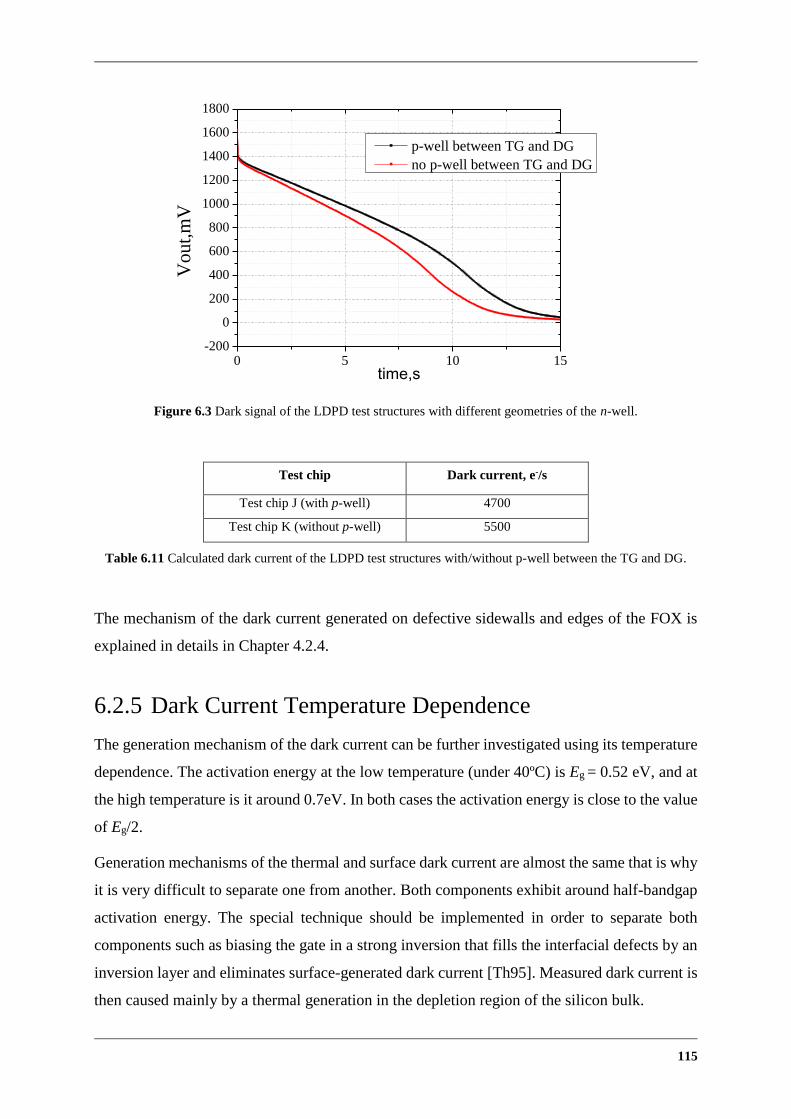
115
Figure 6.3 Dark signal of the LDPD test structures with different geometries of the n-well.
Test chip Dark current, e-/s
Test chip J (with p-well) 4700
Test chip K (without p-well) 5500
Table 6.11 Calculated dark current of the LDPD test structures with/without p-well between the TG and DG.
The mechanism of the dark current generated on defective sidewalls and edges of the FOX is
explained in details in Chapter 4.2.4.
6.2.5 Dark Current Temperature Dependence
The generation mechanism of the dark current can be further investigated using its temperature
dependence. The activation energy at the low temperature (under 40ºC) is Eg = 0.52 eV, and at
the high temperature is it around 0.7eV. In both cases the activation energy is close to the value
of Eg/2.
Generation mechanisms of the thermal and surface dark current are almost the same that is why
it is very difficult to separate one from another. Both components exhibit around half-bandgap
activation energy. The special technique should be implemented in order to separate both
components such as biasing the gate in a strong inversion that fills the interfacial defects by an
inversion layer and eliminates surface-generated dark current [Th95]. Measured dark current is
then caused mainly by a thermal generation in the depletion region of the silicon bulk.
0 5 10 15-200
0
200
400
600
800
1000
1200
1400
1600
1800
Vou
t,m
V
time,s
p-well between TG and DG
no p-well between TG and DG
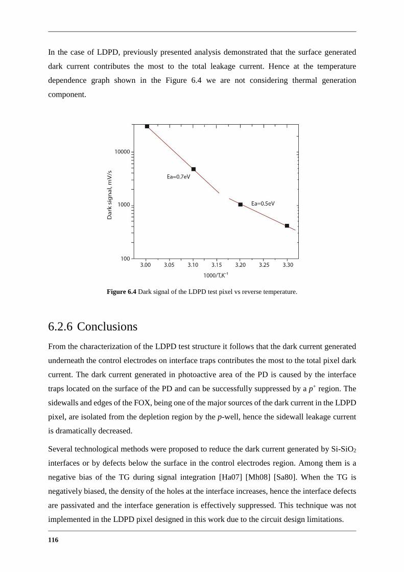
116
In the case of LDPD, previously presented analysis demonstrated that the surface generated
dark current contributes the most to the total leakage current. Hence at the temperature
dependence graph shown in the Figure 6.4 we are not considering thermal generation
component.
Figure 6.4 Dark signal of the LDPD test pixel vs reverse temperature.
6.2.6 Conclusions
From the characterization of the LDPD test structure it follows that the dark current generated
underneath the control electrodes on interface traps contributes the most to the total pixel dark
current. The dark current generated in photoactive area of the PD is caused by the interface
traps located on the surface of the PD and can be successfully suppressed by a p+ region. The
sidewalls and edges of the FOX, being one of the major sources of the dark current in the LDPD
pixel, are isolated from the depletion region by the p-well, hence the sidewall leakage current
is dramatically decreased.
Several technological methods were proposed to reduce the dark current generated by Si-SiO2
interfaces or by defects below the surface in the control electrodes region. Among them is a
negative bias of the TG during signal integration [Ha07] [Mh08] [Sa80]. When the TG is
negatively biased, the density of the holes at the interface increases, hence the interface defects
are passivated and the interface generation is effectively suppressed. This technique was not
implemented in the LDPD pixel designed in this work due to the circuit design limitations.

117
Optimizing control gates geometry also helps to reduce the dark current. Lengths of TG and
CG should be kept as small as possible to reduce the area underneath the gates where the
depletion zone touches Si/SiO2 surface.
6.3 Charge Transfer
The transfer time is an important characteristic of the CMOS line sensor. Fast charge transfer
is one of the requirements for AES application and should be fulfilled to avoid image lag and
provide the feature of the time charge separation.
6.3.7 The Test Structure and Measurement Methodology
An LDPD test array with several 5-pixel test clusters and an output buffer were fabricated using
the 0.35 µm CMOS process in order to evaluate the charge transfer speed. The length of the
pixel photoactive area L = 200 µm with a 10 µm pixel pitch. The length of CG varies from
4.7 µm to 10 µm, the length of TG varies from 3.7 µm to 2 µm. Phosphor has been implanted
to create the n-well with two different implantation doses 2.8 1011 cm-2 and 6 1011 cm-2 ,
energy 350 keV (Table 6.12)
Test chip Pixel pitch,
(µm2)
n-well Implantation Dose
(cm-2), Energy (kEv) CG, (µm)
TG,
(µm) Passivation
Test chip A 10 200 6 1011 ,350 4.7 3.7 Standard
Test chip B 10 200 2.8 1011 ,350 4.7 3.7 Standard
Test chip C 10 200 6 1011 ,350 4.7 2 Standard
Test chip D 10 200 6 1011 ,350 4 3 Standard
Test chip E 10 200 6 1011 ,350 4.7 3.7 Standard
Table 6.12 Varied characteristics of the test chips.
Using measurement setup described in Appendix A the characterizations of the pixel test
structures under different illumination power conditions were performed and analysed to
examine the dependency of the n-well implantation dose, lengths of the control electrodes and
the number of the impinging photons on the charge transfer time.
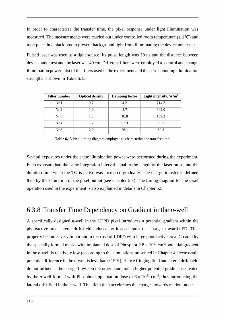
118
In order to characterize the transfer time, the pixel response under light illumination was
measured. The measurements were carried out under controlled room temperature (± 1°C) and
took place in a black box to prevent background light from illuminating the device under test.
Pulsed laser was used as a light source. Its pulse length was 30 ns and the distance between
device under test and the laser was 40 cm. Different filters were employed to control and change
illumination power. List of the filters used in the experiment and the corresponding illumination
strengths is shown in Table 6.13.
Filter number Optical density Damping factor Light intensity, W/m2
Nr 1 0.7 4.2 714.2
Nr 2 1.0 8.7 342.0
Nr 3 1.3 18.8 159.2
Nr 4 1.7 37.3 80.3
Nr 5 2.0 76.1 39.3
Table 6.13 Pixel timing diagram employed to characterize the transfer time.
Several exposures under the same illumination power were performed during the experiment.
Each exposure had the same integration interval equal to the length of the laser pulse, but the
duration time when the TG is active was increased gradually. The charge transfer is defined
then by the saturation of the pixel output (see Chapter 5.5). The timing diagram for the pixel
operation used in the experiment is also explained in details in Chapter 5.5.
6.3.8 Transfer Time Dependency on Gradient in the n-well
A specifically designed n-well in the LDPD pixel introduces a potential gradient within the
photoactive area, lateral drift-field induced by it accelerates the charges towards FD. This
property becomes very important in the case of LDPD with large photoactive area. Created by
the specially formed masks with implanted dose of Phosphor 2.8 1011 cm-2 potential gradient
in the n-well is relatively low (according to the simulations presented in Chapter 4 electrostatic
potential difference in the n-well is less than 0.15 V). Hence fringing field and lateral drift-field
do not influence the charge flow. On the other hand, much higher potential gradient is created
by the n-well formed with Phosphor implantation dose of 6 1011 cm-2, thus introducing the
lateral drift-field in the n-well. This field then accelerates the charges towards readout node.

119
Charge transfer times for the pixels with different implantation doses of the n-well are shown
in Figure 6.5. The transfer time for the pixel with the higher implantation dose of n-well is three
times shorter (ttransfer= 6μs) compared to the charge transfer time of the pixel with the lower
implantation dose of the n-well (ttransfer = 20μs).
Figure 6.5 Transfer time measurements for the pixels with different implantation doses of the n-well.
Illumination power 714.2 W/m2.
The potential gradient generated in the n-well strictly depends on the concentration gradient in
the n-well (on the implantation dose of the n-well). Large induced potential gradient leads to a
higher charge transfer speed.
6.3.9 Transfer Time Dependency on the Number of the
Impinging Photons
Self-induced drift field needs to be considered in the design of the LDPD pixel used for
spectroscopy applications. It is one of the most important mechanisms of the charge transfer.
The emitted spectrum that was to be detected in spectroscopy consists of the lines with different
light intensity, hence the charge transfer time dependence on the illumination power should be
investigated. Analysis of the charge transfer time under high and low intensity of the impinging
radiation was performed. The transfer time varied from 6 μs under 714.2 W/m2 light intensity
to 16 μs under 159.2 W/m2 (Fig. 6.6).
0 5 10 15 20 25 30 350
400
800
1200
1600
V_
FD
[m
V]
t_transfer [s]
Dose 61011cm2
Energy 350keV
Dose 2.81011cm2
Energy 350keV
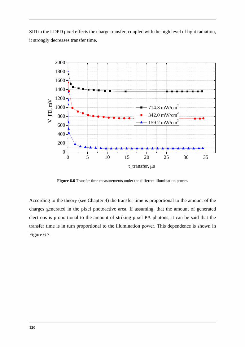
120
SID in the LDPD pixel effects the charge transfer, coupled with the high level of light radiation,
it strongly decreases transfer time.
0 5 10 15 20 25 30 350
200
400
600
800
1000
1200
1400
1600
1800
2000
V_F
D, m
V
t_transfer, s
714.3 mW/cm2
342.0 mW/cm2
159.2 mW/cm2
Figure 6.6 Transfer time measurements under the different illumination power.
According to the theory (see Chapter 4) the transfer time is proportional to the amount of the
charges generated in the pixel photoactive area. If assuming, that the amount of generated
electrons is proportional to the amount of striking pixel PA photons, it can be said that the
transfer time is in turn proportional to the illumination power. This dependence is shown in
Figure 6.7.

121
6 8 10 12 14 16100
200
300
400
500
600
700
800
Illu
min
atio
n p
ow
er,
W/m
2
transfer time, µs
Figure 6.7 Transfer time measurements under the different illumination power.
6.3.10 Transfer Time Dependency on TG and CG length
In the following experiment the dependence of the charge transfer time on the gate length is
evaluated.
As expected from the theoretical observation in Chapter 4, shorter length of the control
electrodes leads to a decrease of the charge transfer time in the pixel. The reason for it is that
the electrons have to travel a shorter distance to reach the FD. Second, smaller electrode lengths
lead to higher fringing fields which in turn minimizes the possibility for trapping/detrapping
mechanism to work, thus a significant improvement in transfer efficiency could be achieved.
In Figure 6.8 measurement results for the LDPD pixels with different electrodes lengths are
shown. The obtained charge transfer time for pixel test structure with CG length
LG,CG = 4.7 μm is 6.8 μs and for the one with CG length LG,CG = 10 μm it is 9.5 μs. The length
of TG is in both cases LG,TG = 3.7 μm.
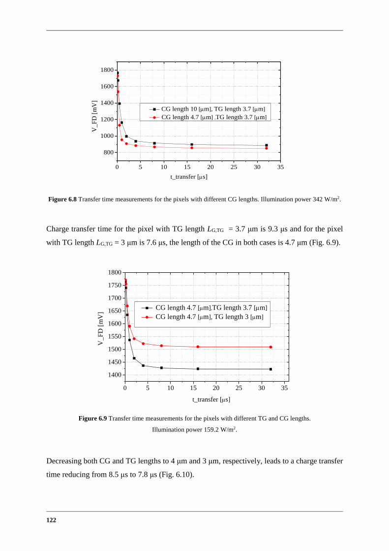
122
Figure 6.8 Transfer time measurements for the pixels with different CG lengths. Illumination power 342 W/m2.
Charge transfer time for the pixel with TG length LG,TG = 3.7 μm is 9.3 μs and for the pixel
with TG length LG,TG = 3 μm is 7.6 μs, the length of the CG in both cases is 4.7 μm (Fig. 6.9).
0 5 10 15 20 25 30 35
1400
1450
1500
1550
1600
1650
1700
1750
1800
t_transfer [s]
V_
FD
[m
V]
CG length 4.7 [m],TG length 3.7 [m]
CG length 4.7 [m], TG length 3 [m]
Figure 6.9 Transfer time measurements for the pixels with different TG and CG lengths.
Illumination power 159.2 W/m2.
Decreasing both CG and TG lengths to 4 μm and 3 μm, respectively, leads to a charge transfer
time reducing from 8.5 μs to 7.8 μs (Fig. 6.10).
0 5 10 15 20 25 30 35
800
1000
1200
1400
1600
1800
V_
FD
[m
V]
t_transfer [s]
CG length 10[m], TG length 3.7[m]
CG length 4.7[m] ,TG length 3.7[m]
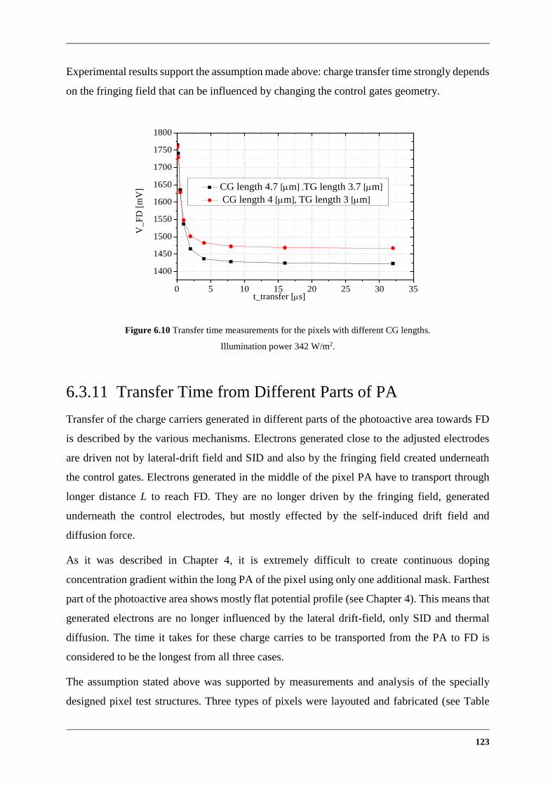
123
Experimental results support the assumption made above: charge transfer time strongly depends
on the fringing field that can be influenced by changing the control gates geometry.
Figure 6.10 Transfer time measurements for the pixels with different CG lengths.
Illumination power 342 W/m2.
6.3.11 Transfer Time from Different Parts of PA
Transfer of the charge carriers generated in different parts of the photoactive area towards FD
is described by the various mechanisms. Electrons generated close to the adjusted electrodes
are driven not by lateral-drift field and SID and also by the fringing field created underneath
the control gates. Electrons generated in the middle of the pixel PA have to transport through
longer distance L to reach FD. They are no longer driven by the fringing field, generated
underneath the control electrodes, but mostly effected by the self-induced drift field and
diffusion force.
As it was described in Chapter 4, it is extremely difficult to create continuous doping
concentration gradient within the long PA of the pixel using only one additional mask. Farthest
part of the photoactive area shows mostly flat potential profile (see Chapter 4). This means that
generated electrons are no longer influenced by the lateral drift-field, only SID and thermal
diffusion. The time it takes for these charge carries to be transported from the PA to FD is
considered to be the longest from all three cases.
The assumption stated above was supported by measurements and analysis of the specially
designed pixel test structures. Three types of pixels were layouted and fabricated (see Table
0 5 10 15 20 25 30 35
1400
1450
1500
1550
1600
1650
1700
1750
1800
V_
FD
[m
V]
t_transfer [s]
CG length 4.7[m] ,TG length 3.7[m]
CG length 4[m], TG length 3[m]
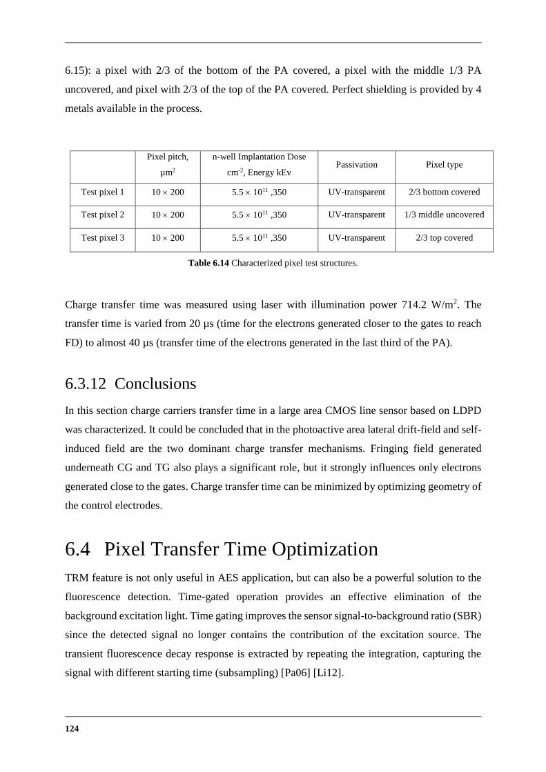
124
6.15): a pixel with 2/3 of the bottom of the PA covered, a pixel with the middle 1/3 PA
uncovered, and pixel with 2/3 of the top of the PA covered. Perfect shielding is provided by 4
metals available in the process.
Pixel pitch,
µm2
n-well Implantation Dose
cm-2, Energy kEv Passivation Pixel type
Test pixel 1 10 200 5.5 1011 ,350 UV-transparent 2/3 bottom covered
Test pixel 2 10 200 5.5 1011 ,350 UV-transparent 1/3 middle uncovered
Test pixel 3 10 200 5.5 1011 ,350 UV-transparent 2/3 top covered
Table 6.14 Characterized pixel test structures.
Charge transfer time was measured using laser with illumination power 714.2 W/m2. The
transfer time is varied from 20 µs (time for the electrons generated closer to the gates to reach
FD) to almost 40 µs (transfer time of the electrons generated in the last third of the PA).
6.3.12 Conclusions
In this section charge carriers transfer time in a large area CMOS line sensor based on LDPD
was characterized. It could be concluded that in the photoactive area lateral drift-field and self-
induced field are the two dominant charge transfer mechanisms. Fringing field generated
underneath CG and TG also plays a significant role, but it strongly influences only electrons
generated close to the gates. Charge transfer time can be minimized by optimizing geometry of
the control electrodes.
6.4 Pixel Transfer Time Optimization
TRM feature is not only useful in AES application, but can also be a powerful solution to the
fluorescence detection. Time-gated operation provides an effective elimination of the
background excitation light. Time gating improves the sensor signal-to-background ratio (SBR)
since the detected signal no longer contains the contribution of the excitation source. The
transient fluorescence decay response is extracted by repeating the integration, capturing the
signal with different starting time (subsampling) [Pa06] [Li12].

125
As it was mentioned above, LDPD pixel built with one additional mask is a good solution for
the AES where the transfer time of 10-40 µs is acceptable. In the fluorescence spectroscopy or
ICP AES applications the charge transfer speed is the limiting factor and the transfer time below
1 µs is required. LDPD line sensor developed in this work could not be any longer considered
as a good candidate to meet such requirements.
6.5 Charge Transfer Improvement
In order to achieve operation without image lag and high-speed transfer, a new pixel design
was proposed. The main idea of the new design is to cut photoactive area in half to shorten the
path electrons have to travel to reach FD. Two sided readout was implemented [Yan04]. The
original photoactive area was divided into two similar 100 µm parts, employing design very
similar to the one used for the existing pixel structure of control electrodes. The doping
concentration profile of the LDPD n-well in proposed new pixel design was optimized. Two
additional implantation steps (respective masks) were added in the process flow chart, each
following the same approach of increasing areas of the neighbouring implantation windows to
reproduce the effect of a "local" generation of lateral drift-fields within each implanted region
of the pixel.
6.5.1 Mask Generation and Pixel Layout
A top view of the proposed pixel configuration layout and the n-well fabrication steps of the
photodetector structure along the cut A-A’ are shown in Figure 6.11. The standard LDPD mask,
that serves to create a non-uniform doping concentration profile of the n-well (mask openings
calculation is described in [Dur10]), was applied during each of the n-well deposition steps.
Three different implantation steps are shown in the Figure 6.12 with the different colours.

126
Figure 6.11 New pixel configuration layout and n-well fabrication steps.
Three implantation steps, that are forming the n-well in the proposed pixel structure, are shown
in details in Figure 6.12. Masks from (1) to (3) were implemented.
Figure 6.12 Implantation steps forming newly designed n-well.
To assure the proper charge transfer towards TG and block the charge flow towards DG, the
original end doping concentration of the LDPD n-well, labelled N3 in the new approach, was
implanted in the third of the photoactive area in front of CG and beneath CG-TG-FD
(see Fig. 6.12). The middle third part of the photoactive area had doping concentration N2 lower
than N3 according to the relation N3 = N2 + ΔN, where ΔN represents the increment in the donor
doping concentration in N3 relative to N2. Finally, the last third of the photoactive area (the most
separated from the CG) had doping concentration N1, lower than N2, and following the very
similar relation to N2: N2 = N1 + ΔN.
127
Three implants result in a graded potential profile along the photodetector as shown in details
in Figure 6.13. The p+-layer introduced in PA for the same purpose as in original LDPD pixel
design.
The potential profile of the proposed n-well is illustrated in Figure 6.13. The donor
concentration of the n-well increases along the photoactive area of the pixel reaching its
maximum beneath CG. The proposed graded potential profile of the n-well divides the
photoactive area of the pixel to three parts. In each of the parts the n-well potential profile is
not constant due to the LDPD mask approach implemented "locally". The enhanced lateral
drift-field induced within each part of the n-well accelerates the charge carriers, decreasing the
overall charge transfer time. The more efficient charge transfer is achieved compared to the
pixel designs described for example by Kosonocky [Ko96] [Ko97] [Jar01]. There the similar
grated potential in the n-well was introduced, but the charge transport within several constant
potential regions is governed only by the thermal diffusion, no additional LDPD mask was
implemented.
The potential profile in the N2 region acts as a charge sink for the N1 region and the N3 region
acts as a charge sink for the N2. At the edge of the N3 region an additional fringing field is
generated through the influence of CG. Reducing CG area increases the fringing field that arises
at its edge in the direction of TG or DG (see Fig. 6.13). It is generated by TG or DG bias
voltages respectively. Due to the potential difference between the adjacent edges of the N1, N2,
and N3 regions the additional fringing fields are introduced in the n-well (see Fig. 6.13)
improving the transfer efficiency.

128
Figure 6.13 Proposed pixel design and electrostatic potential diagram of the pixel.
6.5.2 Simulation of the Doping Concentration Profile
Doping concentration in the proposed pixel design was simulated using Synopsys TCAD. The
PA of the pixel was chosen to be 100 µm, spaced into three same length regions to create the
graded doping concentration profile. For the n-well, the three Phosphor implantation doses (N1,
N2, and N3) were used with the identical implantation energy, ΔN = 0.51011 cm-2. LDPD mask
was implemented to create lateral drift-filed within each region of the PA.
In Figure 6.14 doping concentration profile of the proposed pixel configuration is shown. The
n-well is implanted in the following way: implant dose N1 = 41011 cm-2, N2 = 4.51011 cm-2
and N3 = 51011 cm-2. The doping concentration of the n-well is increasing along the x-axis.
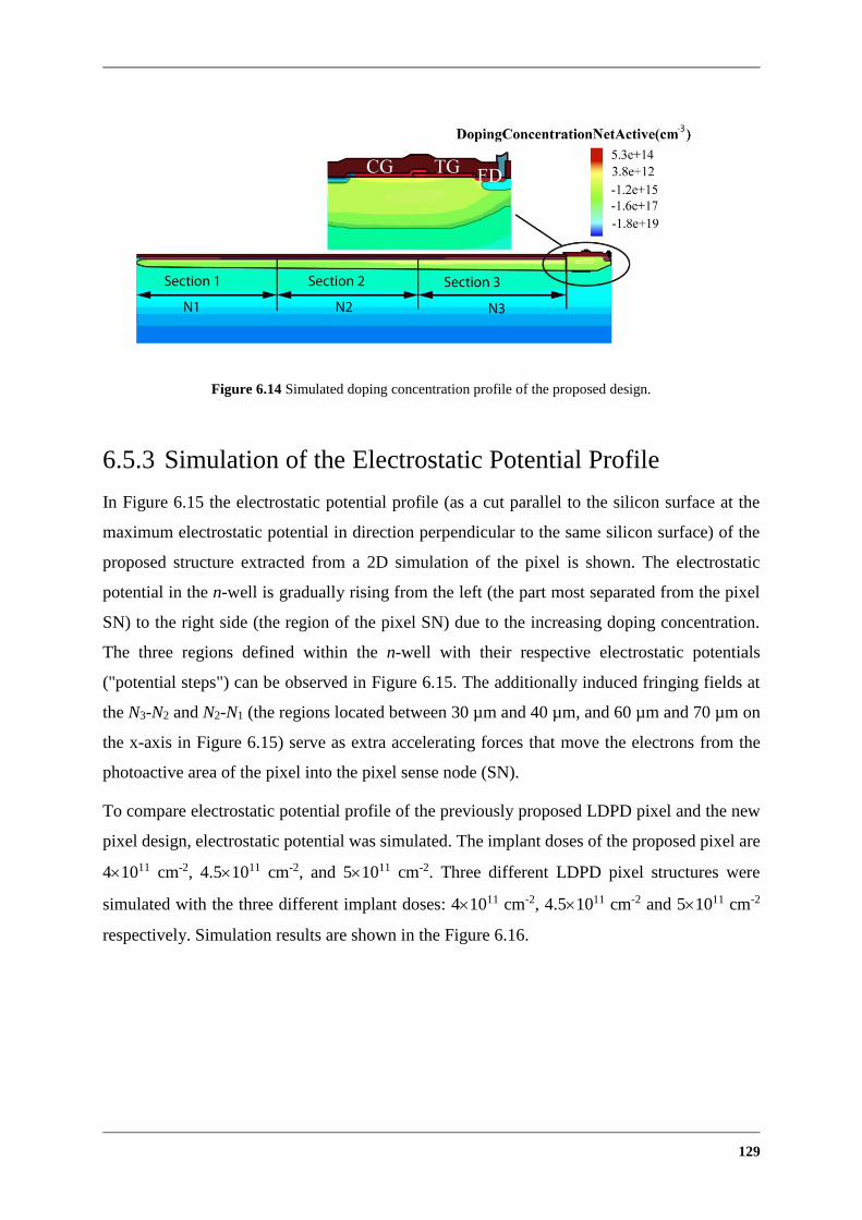
129
Figure 6.14 Simulated doping concentration profile of the proposed design.
6.5.3 Simulation of the Electrostatic Potential Profile
In Figure 6.15 the electrostatic potential profile (as a cut parallel to the silicon surface at the
maximum electrostatic potential in direction perpendicular to the same silicon surface) of the
proposed structure extracted from a 2D simulation of the pixel is shown. The electrostatic
potential in the n-well is gradually rising from the left (the part most separated from the pixel
SN) to the right side (the region of the pixel SN) due to the increasing doping concentration.
The three regions defined within the n-well with their respective electrostatic potentials
("potential steps") can be observed in Figure 6.15. The additionally induced fringing fields at
the N3-N2 and N2-N1 (the regions located between 30 µm and 40 µm, and 60 µm and 70 µm on
the x-axis in Figure 6.15) serve as extra accelerating forces that move the electrons from the
photoactive area of the pixel into the pixel sense node (SN).
To compare electrostatic potential profile of the previously proposed LDPD pixel and the new
pixel design, electrostatic potential was simulated. The implant doses of the proposed pixel are
41011 cm-2, 4.51011 cm-2, and 51011 cm-2. Three different LDPD pixel structures were
simulated with the three different implant doses: 41011 cm-2, 4.51011 cm-2 and 51011 cm-2
respectively. Simulation results are shown in the Figure 6.16.

130
Figure 6.15 Simulated potential profile of the proposed design.
The maximum electrostatic potential difference achieved across the entire photoactive area of
the original LDPD pixel is 0.4 V (for the n-well with the higher implant dose), while the
electrostatic potential difference in the new pixel design is almost 0.75 V (see Fig. 6.16). The
maximum potential in both structures is the same. It is limited by the shutter efficiency of the
TG and the DG. In the new design each of the three regions can be tailored separately. This
enables the ability of optimization each of the implantation region to create the maximum
concentration gradient. Due to a larger potential difference within the n-well in the new pixel
structure, higher acceleration of the charge carriers can be achieved.
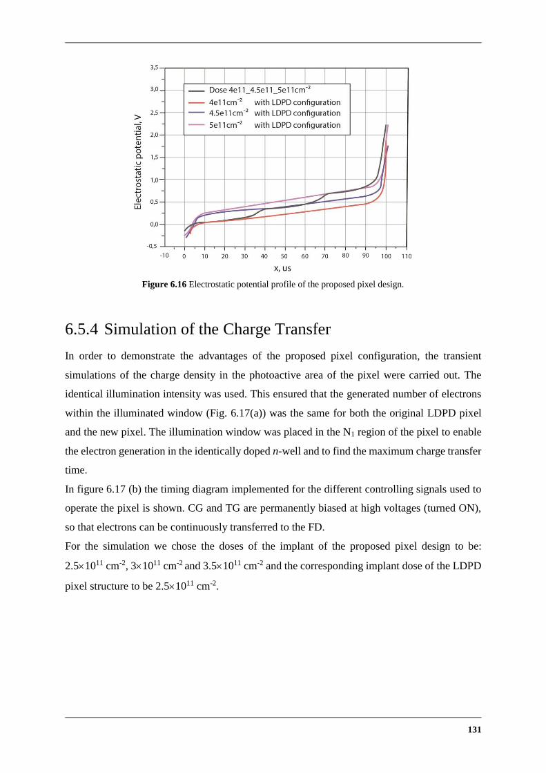
131
Figure 6.16 Electrostatic potential profile of the proposed pixel design.
6.5.4 Simulation of the Charge Transfer
In order to demonstrate the advantages of the proposed pixel configuration, the transient
simulations of the charge density in the photoactive area of the pixel were carried out. The
identical illumination intensity was used. This ensured that the generated number of electrons
within the illuminated window (Fig. 6.17(a)) was the same for both the original LDPD pixel
and the new pixel. The illumination window was placed in the N1 region of the pixel to enable
the electron generation in the identically doped n-well and to find the maximum charge transfer
time.
In figure 6.17 (b) the timing diagram implemented for the different controlling signals used to
operate the pixel is shown. CG and TG are permanently biased at high voltages (turned ON),
so that electrons can be continuously transferred to the FD.
For the simulation we chose the doses of the implant of the proposed pixel design to be:
2.51011 cm-2, 31011 cm-2 and 3.51011 cm-2 and the corresponding implant dose of the LDPD
pixel structure to be 2.51011 cm-2.
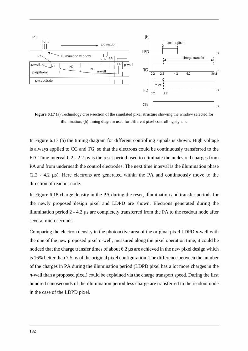
132
Figure 6.17 (a) Technology cross-section of the simulated pixel structure showing the window selected for
illumination; (b) timing diagram used for different pixel controlling signals.
In Figure 6.17 (b) the timing diagram for different controlling signals is shown. High voltage
is always applied to CG and TG, so that the electrons could be continuously transferred to the
FD. Time interval 0.2 - 2.2 µs is the reset period used to eliminate the undesired charges from
PA and from underneath the control electrodes. The next time interval is the illumination phase
(2.2 - 4.2 µs). Here electrons are generated within the PA and continuously move to the
direction of readout node.
In Figure 6.18 charge density in the PA during the reset, illumination and transfer periods for
the newly proposed design pixel and LDPD are shown. Electrons generated during the
illumination period 2 - 4.2 µs are completely transferred from the PA to the readout node after
several microseconds.
Comparing the electron density in the photoactive area of the original pixel LDPD n-well with
the one of the new proposed pixel n-well, measured along the pixel operation time, it could be
noticed that the charge transfer times of about 6.2 µs are achieved in the new pixel design which
is 16% better than 7.5 µs of the original pixel configuration. The difference between the number
of the charges in PA during the illumination period (LDPD pixel has a lot more charges in the
n-well than a proposed pixel) could be explained via the charge transport speed. During the first
hundred nanoseconds of the illumination period less charge are transferred to the readout node
in the case of the LDPD pixel.

133
Figure 6.18 Transient simulation results show the change of the carrier concentration density in the photoactive
area of the original LDPD and the proposed pixel.
Three different configurations of the novel pixel design were simulated. In Figure 6.19 the
results from the transient simulations are shown. Comparing the electron density in the PA in
all three cases, configuration with the implantation doses 3.51011cm-2, 41011cm-2, 4.51011
cm-2 appeared to show the fastest transfer, with the minimum charge carrier transfer time of
about 5.2 µs.
Figure 6.19 Transient simulations of the proposed pixel design with different implants concentrations.

134
6.5.5 Conclusions
According to the presented simulation results the charge transfer time in the proposed new pixel
design is decreased and the possibility of the image lag to appear is minimized. Unfortunately,
SID mechanisms related to the charge transfer were not taken into account in the simulations
(the illumination was chosen too low for these effects to be observed). Hence, the obtained
results can only qualitatively show that the new designed n-well provides faster charge transfer
compared to the original LDPD design. In reality, the expected transfer time under higher
irradiances (typically used in AES applications) will be shorter than 5 µs mainly due to SID
effects.
6.6 Crosstalk
Crosstalk in CMOS line sensor is a challenging problem to handle. It limits the spatial resolution
and reduces the overall sensitivity of the sensor. Crosstalk can be divided into two main parts:
the electrical crosstalk and the optical crosstalk. To the best knowledge of author of this work,
pixel crosstalk between large area pixels in CMOS sensors has not been investigated before.
Various research groups were previously concentrating on the characterization of the pixels
with sizes below 3 µm2, normally driven by the high spatial resolution demand from the
consumer market [Wa01] [Ag03] [Br02]. In this Chapter electrical and optical crosstalk on the
LDPD CMOS line sensor are evaluated.
6.6.1 Test Structure and Measurement Methodology
A set of test structures was developed to evaluate the electrical crosstalk. Each test structure
consists of 1 row with 368 LDPD pixels of identical size but varying types of metal shielding.
368 pixels of each test chip are divided into several groups. Each group consists of 11 pixels,
the layouts of which are schematically shown in Figure 6.20. All pixels in the test structures
shown in Figure 6.21 except for the central one were optically shielded using all four metal
layers available in the process.
In order to characterize the electrical crosstalk between the neighbouring pixels the optical
crosstalk must be eliminated. This is why high quality optical shielding is required.
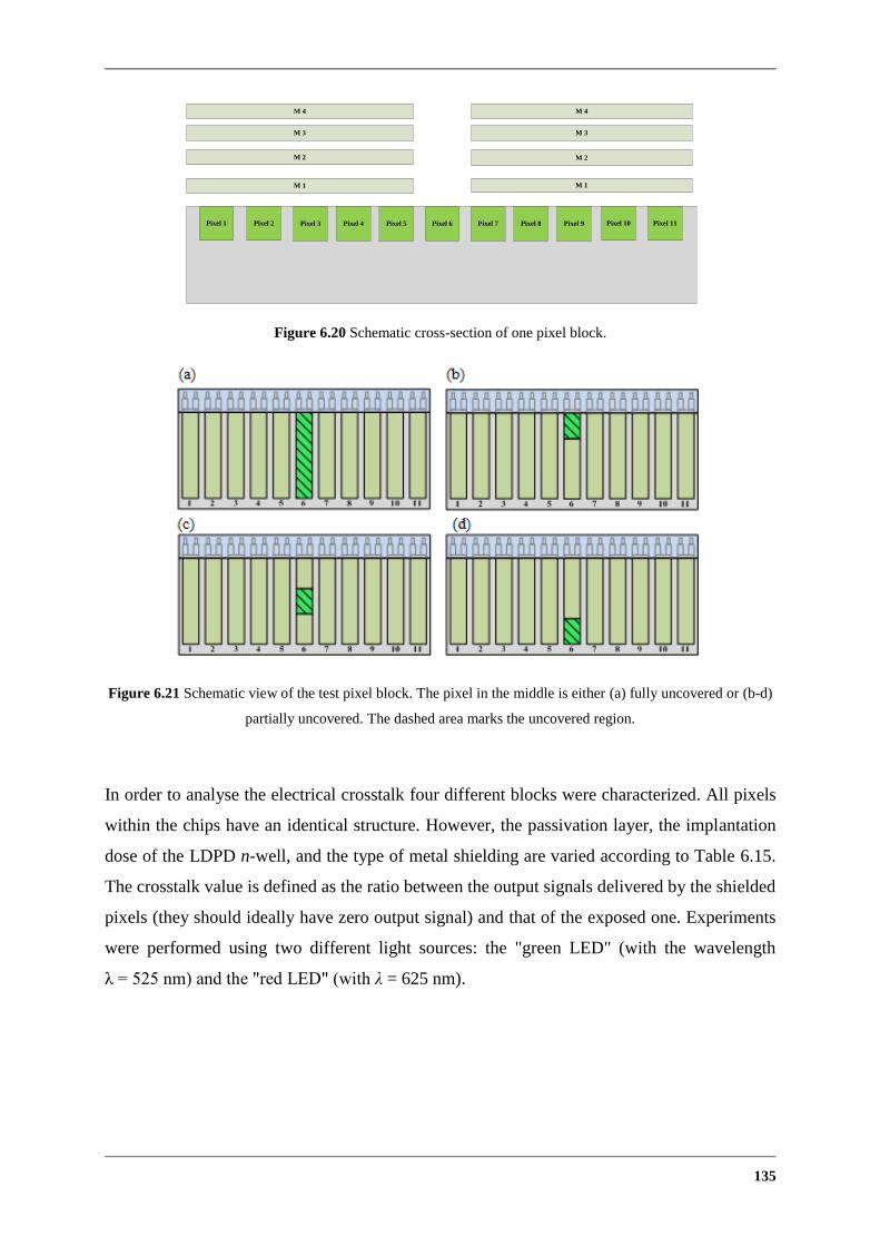
135
Figure 6.20 Schematic cross-section of one pixel block.
Figure 6.21 Schematic view of the test pixel block. The pixel in the middle is either (a) fully uncovered or (b-d)
partially uncovered. The dashed area marks the uncovered region.
In order to analyse the electrical crosstalk four different blocks were characterized. All pixels
within the chips have an identical structure. However, the passivation layer, the implantation
dose of the LDPD n-well, and the type of metal shielding are varied according to Table 6.15.
The crosstalk value is defined as the ratio between the output signals delivered by the shielded
pixels (they should ideally have zero output signal) and that of the exposed one. Experiments
were performed using two different light sources: the "green LED" (with the wavelength
λ = 525 nm) and the "red LED" (with λ = 625 nm).
Pixel 3
M 1 M 1
M 2 M 2
Pixel 9Pixel 4 Pixel 5 Pixel 7 Pixel 8Pixel 6
M 3 M 3
M 4 M 4
Pixel 2 Pixel 11Pixel 10Pixel 1
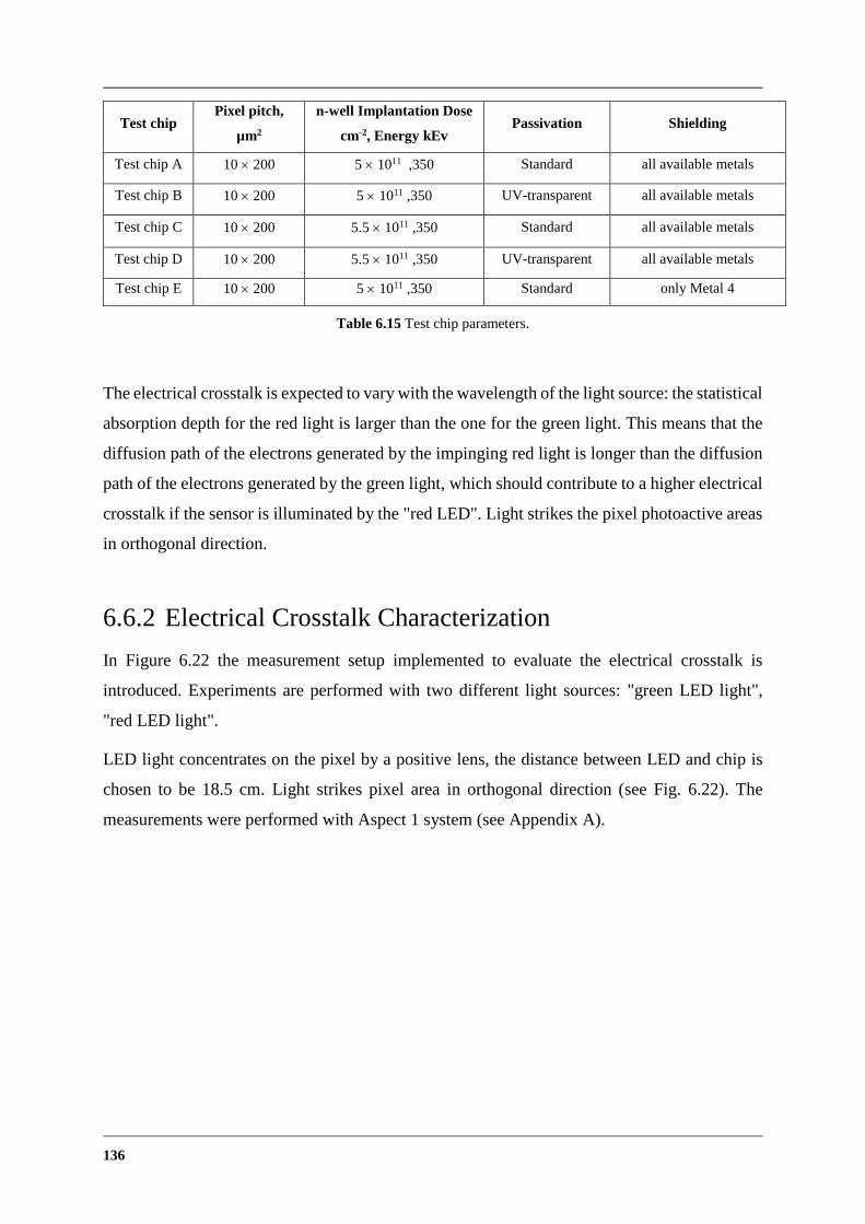
136
Test chip Pixel pitch,
µm2
n-well Implantation Dose
cm-2, Energy kEv Passivation Shielding
Test chip A 10 200 5 1011 ,350 Standard all available metals
Test chip B 10 200 5 1011 ,350 UV-transparent all available metals
Test chip C 10 200 5.5 1011 ,350 Standard all available metals
Test chip D 10 200 5.5 1011 ,350 UV-transparent all available metals
Test chip E 10 200 5 1011 ,350 Standard only Metal 4
Table 6.15 Test chip parameters.
The electrical crosstalk is expected to vary with the wavelength of the light source: the statistical
absorption depth for the red light is larger than the one for the green light. This means that the
diffusion path of the electrons generated by the impinging red light is longer than the diffusion
path of the electrons generated by the green light, which should contribute to a higher electrical
crosstalk if the sensor is illuminated by the "red LED". Light strikes the pixel photoactive areas
in orthogonal direction.
6.6.2 Electrical Crosstalk Characterization
In Figure 6.22 the measurement setup implemented to evaluate the electrical crosstalk is
introduced. Experiments are performed with two different light sources: "green LED light",
"red LED light".
LED light concentrates on the pixel by a positive lens, the distance between LED and chip is
chosen to be 18.5 cm. Light strikes pixel area in orthogonal direction (see Fig. 6.22). The
measurements were performed with Aspect 1 system (see Appendix A).
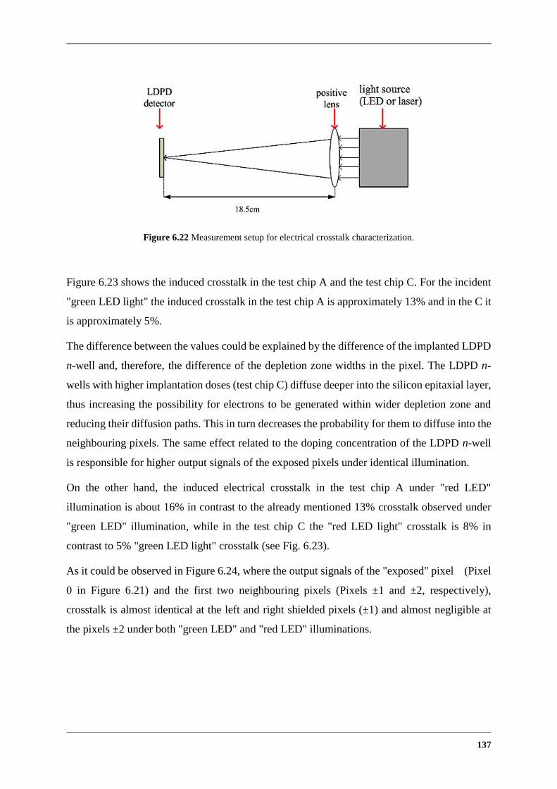
137
Figure 6.22 Measurement setup for electrical crosstalk characterization.
Figure 6.23 shows the induced crosstalk in the test chip A and the test chip C. For the incident
"green LED light" the induced crosstalk in the test chip A is approximately 13% and in the C it
is approximately 5%.
The difference between the values could be explained by the difference of the implanted LDPD
n-well and, therefore, the difference of the depletion zone widths in the pixel. The LDPD n-
wells with higher implantation doses (test chip C) diffuse deeper into the silicon epitaxial layer,
thus increasing the possibility for electrons to be generated within wider depletion zone and
reducing their diffusion paths. This in turn decreases the probability for them to diffuse into the
neighbouring pixels. The same effect related to the doping concentration of the LDPD n-well
is responsible for higher output signals of the exposed pixels under identical illumination.
On the other hand, the induced electrical crosstalk in the test chip A under "red LED"
illumination is about 16% in contrast to the already mentioned 13% crosstalk observed under
"green LED" illumination, while in the test chip C the "red LED light" crosstalk is 8% in
contrast to 5% "green LED light" crosstalk (see Fig. 6.23).
As it could be observed in Figure 6.24, where the output signals of the "exposed" pixel (Pixel
0 in Figure 6.21) and the first two neighbouring pixels (Pixels ±1 and ±2, respectively),
crosstalk is almost identical at the left and right shielded pixels (±1) and almost negligible at
the pixels ±2 under both "green LED" and "red LED" illuminations.

138
Figure 6.23 Wavelength dependent electrical crosstalk for LDPD pixel test-structures with lower implantation
dose (test chip A), and slightly higher implantation dose (test chip C).
Figure 6.24 Pixel crosstalk test results. Pixel 0 is active, pixels ±1, ±2 are optically black.
In the LDPD-based pixel structures the transport of electrons from the photoactive area (the
region of the LDPD n-well) through CG, TG or DG regions into FD or DD results from: thermal
diffusion, the lateral drift induced through the intrinsic concentration gradient within the LDPD
n-well, the transport mechanisms associated with the self-induced drift-field (SID), generated
by the electrons travelling across the pixel, and the fringing fields, induced between the
neighbouring implantation windows of the LDPD n-well extra mask or at the edges of the CG
and both transfer-gates (see Chapter 4).
If the long photoactive area of the LDPD pixel is considered, the electrons are most likely not
influenced by the intrinsic lateral drift-field within entire 200 µm of length, especially in the
area most separated from CG region where the doping concentration of the LDPD n-well is
quite low and no fringing fields due to the biasing of CG can be sensed. In this region electrons
are transported mainly by the thermal diffusion mechanisms. Being no longer influenced by the
lateral drift-field, electrons could theoretically diffuse into the neighbouring pixel n-wells or
FDs. To verify this assumption, measurement results from the test-blocks 2, 3, and 4 (shown in
Figure 6.21 (b), (c) and (d)) test chips A and C were analysed.
Green Red0
5
10
15
20
cro
ssta
lk, %
wavelenght
test chip A(a)
test chip C(b)
-2 -1 0 1 2
0
20
40
60
80
100
"green LED"
cro
ssta
lk,%
pixel
test chip A
test chip C
-2 -1 0 1 2
0
20
40
60
80
100
"red LED"
cro
ssta
lk,%
pixel
test chip A
test chip C
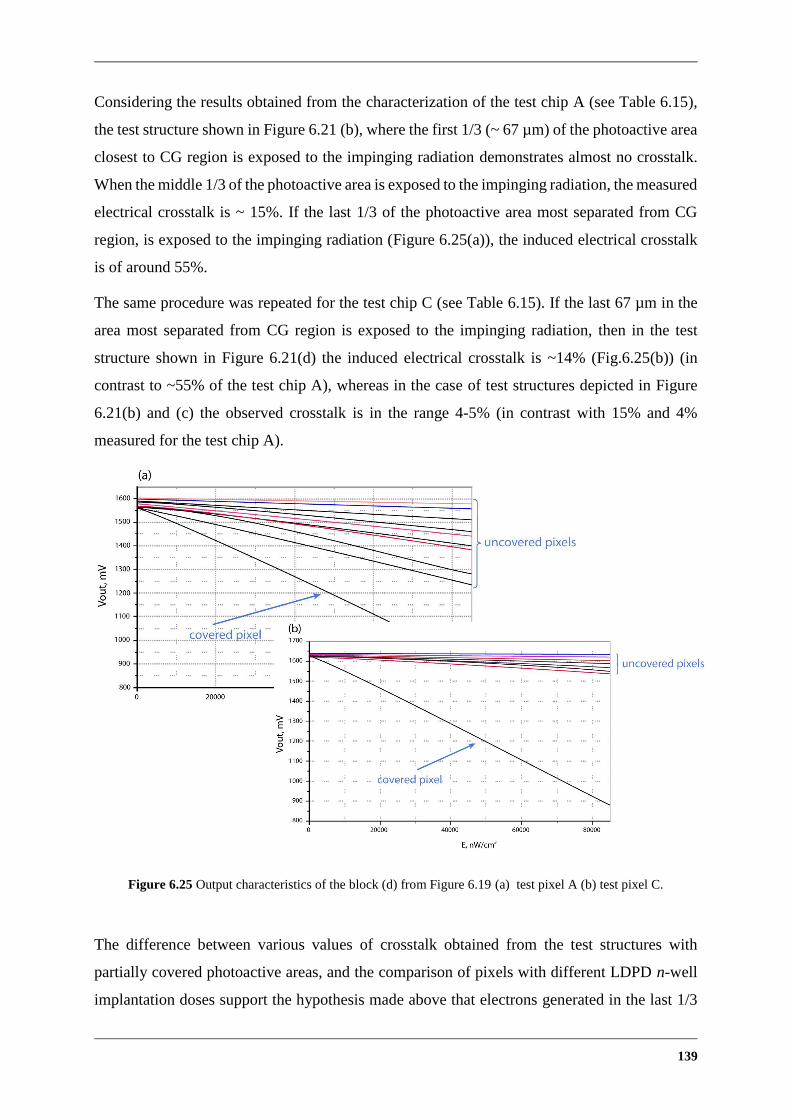
139
Considering the results obtained from the characterization of the test chip A (see Table 6.15),
the test structure shown in Figure 6.21 (b), where the first 1/3 (~ 67 µm) of the photoactive area
closest to CG region is exposed to the impinging radiation demonstrates almost no crosstalk.
When the middle 1/3 of the photoactive area is exposed to the impinging radiation, the measured
electrical crosstalk is ~ 15%. If the last 1/3 of the photoactive area most separated from CG
region, is exposed to the impinging radiation (Figure 6.25(a)), the induced electrical crosstalk
is of around 55%.
The same procedure was repeated for the test chip C (see Table 6.15). If the last 67 µm in the
area most separated from CG region is exposed to the impinging radiation, then in the test
structure shown in Figure 6.21(d) the induced electrical crosstalk is ~14% (Fig.6.25(b)) (in
contrast to ~55% of the test chip A), whereas in the case of test structures depicted in Figure
6.21(b) and (c) the observed crosstalk is in the range 4-5% (in contrast with 15% and 4%
measured for the test chip A).
Figure 6.25 Output characteristics of the block (d) from Figure 6.19 (a) test pixel A (b) test pixel C.
The difference between various values of crosstalk obtained from the test structures with
partially covered photoactive areas, and the comparison of pixels with different LDPD n-well
implantation doses support the hypothesis made above that electrons generated in the last 1/3
140
of the pixel photoactive are have the highest chance to diffuse to the neighbouring pixels
n-wells. In the test chip with the higher dose of n-well implant (test chip C) drift field is induced
in the last 1/3 of the pixel area and influenced charge carriers not letting them to diffuse to the
adjustment pixel n-well, hence electrical cross talk is reduced if compared to the test chip A.
Thus for LDPD-based pixels with long photoactive areas the n-well should be carefully
designed in order to assure that the electrons generated in any region of the photoactive area
are constantly influenced by the lateral drift-field. This includes paying a lot of attention to the
design of the LDPD n-well mask and correctly choose the implantation parameters in order to
maximize the pixel sensitivity and minimize the electrical crosstalk.
6.6.3 Optical Crosstalk Characterization
Optical crosstalk was with two different measurements. In the first experiment "green LED"
radiation strikes the pixel in the direction orthogonal to the silicon surface of two test chips: test
chip C with the standard passivation and test chip D with the UV-transparent passivation (see
Table 6.15). The measurements performed using Aspect 1 system (see Appendix A).
Induced crosstalk in the test chip C is ~ 5% and in the test chip D it is ~ 4%. The difference
between the values could be explained by the difference of the pixel passivation layers.
UV-transparent passivation is designed to have less absorption and reflection compared to the
standard passivation. Thus more photons are able to reach the PD surface thereby increasing
the detector sensitivity and reducing the optical crosstalk, hence increasing the signal of the
uncovered pixel.
The second measurement was performed to analyze the radiation incident angle-dependent
optical crosstalk. Experiments were performed using "green LED" illumination with incidence
angles of 0°, ± 10°, ± 30° (see Fig. 6.26). They were conducted only on the test chip E in order
to better optical crosstalk due to the imperfect light shielding of the used single Metal 4 (the
last metal layer in the process and the one most separated from the silicon surface).

141
Figure 6.26 Measurement setup used to evaluate electrical crosstalk.
The measured induced crosstalk for the test chip E was of about 27%. Taking into consideration
that the electrical crosstalk measured on the identical pixel block was of ~ 13%, it can be
calculated that the optical crosstalk was actually ~14% considering all the angles of incidence
mentioned.
When light strikes the pixel area under an angle different from 0°, the induced optical crosstalk
will increases as expected. For "green LED light" radiation impinging at an angle 30° (as shown
in Fig. 6.27(a)), the measured crosstalk is ~72%, as it can be observed in the incident radiation
impinging angle-dependent crosstalk curve shown in Figure 6.28. At -30° (as shown in
Fig. 6.27(b)) incident angle, the induced crosstalk ~60%, as it can be observed in Figure 6.28.
As expected, with the increased optical crosstalk the output signal of the uncovered pixel
decreases. Reduction of the sensitivity is the result of the increase of the light incidence angle,
hence lower amount of photons actually reaches the photoactive area of the uncovered pixel
and more photons are thus impinging the neighboring pixels’ active areas. A logical side-effect
of this phenomenon is of course, the increase of the output signal of the neighboring covered
pixels.
LDPD
detector
positive lens
α= 30°or 10°
α
-α
LED light
(green)
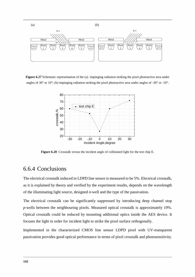
142
(a) (b)
Figure 6.27 Schematic representation of the (a) impinging radiation striking the pixel photoactive area under
angles of 30° or 10°; (b) impinging radiation striking the pixel photoactive area under angles of -30° or -10°.
Figure 6.28 Crosstalk versus the incident angle of collimated light for the test chip E.
6.6.4 Conclusions
The electrical crosstalk induced in LDPD line sensor is measured to be 5%. Electrical crosstalk,
as it is explained by theory and verified by the experiment results, depends on the wavelength
of the illuminating light source, designed n-well and the type of the passivation.
The electrical crosstalk can be significantly suppressed by introducing deep channel stop
p-wells between the neighbouring pixels. Measured optical crosstalk is approximately 19%.
Optical crosstalk could be reduced by mounting additional optics inside the AES device. It
focuses the light in order for incident light to strike the pixel surface orthogonally.
Implemented in the characterized CMOS line sensor LDPD pixel with UV-transparent
passivation provides good optical performance in terms of pixel crosstalk and photosensitivity.
Dummy
pixel
Pixel
1Dummy
pixel
Pixel
2
Pixel
3
Pixel
4
Pixel
5
Metal Metal
h·v
Dummy
pixel
Pixel
1Dummy
pixel
Pixel
2
Pixel
3
Pixel
4
Pixel
5
Metal Metal
h·v
-30 -20 -10 0 10 20 3020
30
40
50
60
70
80
cro
ssta
lk,%
Incident Angle,degree
test chip E

143
7 CMOS Line Sensor with 1 x 368 Pixels
A 1 × 368 pixels CMOS line sensor was designed and fabricated in a 0.35 µm CMOS
technology (see for layout Fig. 7.1), with the an extra n-well yielding a non-uniform lateral
doping profile and an additional p+ surface layer fabricated on top of it to pin the surface to the
silicon substrate potential. On the line sensor 368 pixels in the line sensor are divided into four
blocks, each containing 92 pixels. All four pixel blocks consist of identical pixels with the
length of the photoactive area L = 200 µm. The chip area is of 1.77 x 4.65 mm2. The distance
between the n-wells of the neighboring pixels is 5.5 μm for a 10 μm pixel pitch. Detailed
description, optical and electrical characteristics of the pixels are presented in Chapter 6.
Figure 7.1 CMOS line sensor with 1 x 368 pixels.
7.1 Circuit and Sensor Design
Figure 7.2 shows the building block of the sensor as a diagram. The output line of each pixel
P<i> is connected to the analog switch SEL_FD. The shift register activates only one analog
switch per clock cycle CLK_MUX. It also sets the output voltage of the connected pixel to the
input of the output buffer. The pixel output appears on the pin OUT_SENSOR.
Figure 7.3 shows the circuit diagram of the pixel. The source follower (SF1) and reset transistor
(RESET_FD) are connected to the separate supply voltages VDDA and VDDPIX, respectively.
Such connection allows them to be controlled independently. Two transfer gates connect pixel
photoactive area to the floating diffusion (for the transfer gate) and the draining diffusion (for
the draining gate). DG is controlled via an external digital signal to enabling or disabling the
discharge of the photoactive area into the drain diffusion, which permanently biased to the
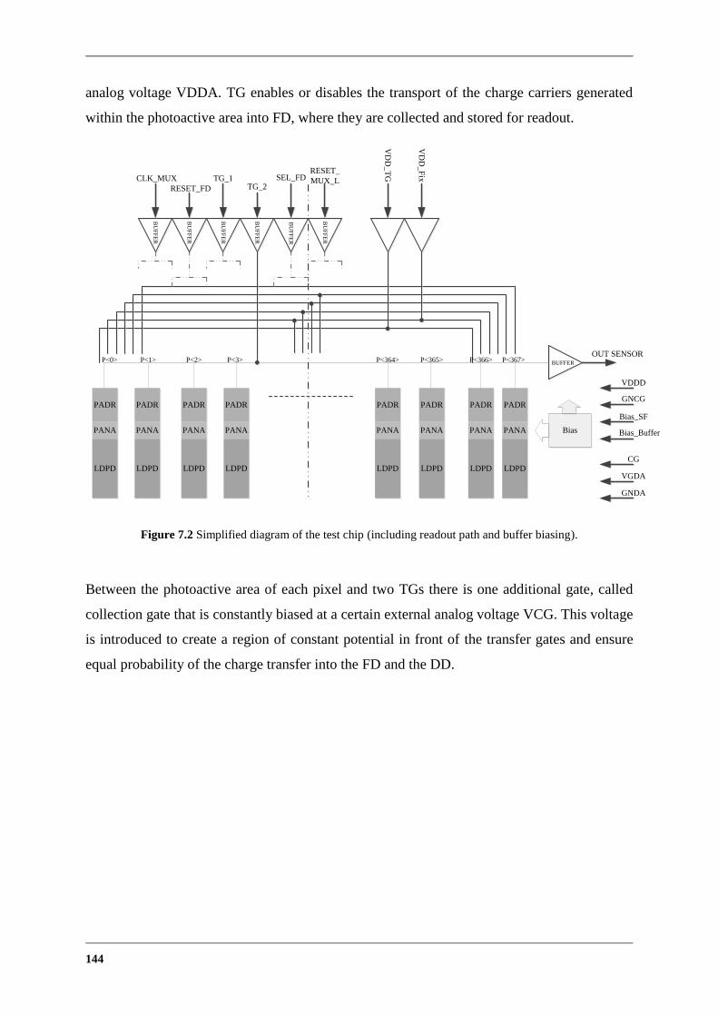
144
analog voltage VDDA. TG enables or disables the transport of the charge carriers generated
within the photoactive area into FD, where they are collected and stored for readout.
Figure 7.2 Simplified diagram of the test chip (including readout path and buffer biasing).
Between the photoactive area of each pixel and two TGs there is one additional gate, called
collection gate that is constantly biased at a certain external analog voltage VCG. This voltage
is introduced to create a region of constant potential in front of the transfer gates and ensure
equal probability of the charge transfer into the FD and the DD.
PADR
PANA
LDPD
PADR
PANA
LDPD
PADR
PANA
LDPD
PADR
PANA
LDPD
PADR
PANA
LDPD
PADR
PANA
LDPD
PADR
PANA
LDPD
PADR
PANA
LDPD
Bias
BUFFER
GNDA
VGDA
CG
Bias_Buffer
Bias_SF
GNCG
VDDD
OUT SENSOR
BU
FF
ER
BU
FF
ER
BU
FF
ER
BU
FF
ER
BU
FF
ER
BU
FF
ER
CLK_MUX
RESET_FD
TG_1TG_2
SEL_FDRESET_
MUX_L
VD
D_
TG
VD
D_
Fix
P<0> P<1> P<2> P<3> P<364> P<365> P<366> P<367>

145
Figure 7.3 Circuit diagram of the LDPD-based pixel used for the line sensor development.
7.2 Pixel Characteristics
The pixel structure parameters used in CMOS line sensor are available in the Table 7.1. Chips
from four different wafers were bonded and measured. These measurements are presented in
Table 7.2.
Pixel pitch,
µm2
n-well
overlap
SF w/l
(µm)
n-well
(µm)
CG(µm) TG(µm) FD
(µm)
RST
10 x 200 0.8 2/1 56 4.7 x 5.9 3.7 2.1 x 1 PEDIG
Table 7.1. Pixel parameters.
DFFADR<i> ADR<i-1>
RESET_MUX_L
CLK_MUX
TG2
TG1
RESET_FDSEL_FD
VDDPIX
RESET
VDDA
SF1
(FDn)n+CFD
GNDA
TG
DG
VCG
CG
M1
GNDA
IBAIS_SF
INV INV INV INV
SELECT SELECT
P<i>
1
GNDA
LDPD
Photo-
activearea
(DDn)n+VDDA
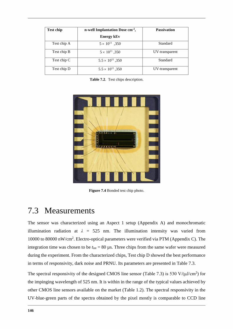
146
Test chip n-well Implantation Dose cm-2,
Energy kEv
Passivation
Test chip A 5 1011 ,350 Standard
Test chip B 5 1011 ,350 UV-transparent
Test chip C 5.5 1011 ,350 Standard
Test chip D 5.5 1011 ,350 UV-transparent
Table 7.2. Test chips description.
Figure 7.4 Bonded test chip photo.
7.3 Measurements
The sensor was characterized using an Aspect 1 setup (Appendix A) and monochromatic
illumination radiation at λ = 525 nm. The illumination intensity was varied from
10000 to 80000 nW/cm2. Electro-optical parameters were verified via PTM (Appendix C). The
integration time was chosen to be tint = 80 µs. Three chips from the same wafer were measured
during the experiment. From the characterized chips, Test chip D showed the best performance
in terms of responsivity, dark noise and PRNU. Its parameters are presented in Table 7.3.
The spectral responsivity of the designed CMOS line sensor (Table 7.3) is 530 V/(μJ/cm2) for
the impinging wavelength of 525 nm. It is within in the range of the typical values achieved by
other CMOS line sensors available on the market (Table 1.2). The spectral responsivity in the
UV-blue-green parts of the spectra obtained by the pixel mostly is comparable to CCD line

147
sensors. This can be explained by a well-tailored interface of the surface pinning p+ layer and
the LDPD n-well, correctly chosen value of the sense node capacitance, and mainly by a
specially developed UV-enhanced silicon-nitride based passivation layer used in the CMOS
process. This passivation additionally serves as the antireflective coating for these wavelengths.
The detailed explanation is given in Chapter 5 and Chapter 6.
The dark current parameters were measured by varying the integration time of the sensor while
it remained unexposed to light. A linear time dependence slope of the mean dark output signal
of the pixel, measured using the chosen integration times, is found to be 75 mV/s at 22°C, i.e.
36 pA/cm2 or 4400 e-/s, for the given pixel area and the linear sensor conversion
gain of 17μV/e-.This relatively low dark current performance in the developed CMOS line
sensor is the result of several optimizations steps including the addition of the surface p+
pinning layer on top of the LDPD n-well in the photoactive area of the pixel, introduction of
several deep p-well channel-stops between the neighboring pixels, carefully chosen length and
width of the control electrodes (CG, TG, and DG), and a adapted design of FD (Chapter 6).
PRNU and DSNU are two parameters that were not fully characterized by the developed test
structures. Test pixel structures that were manufactured and measured (Chapter 6), contain only
5 pixels and cannot deliver enough information about the non-uniformities.
The phenomenon defined originally as the Fixed Pattern Noise (FPN) is a very serious problem
in CMOS imagers due to threshold voltage variations of the MOSFET transistors (especially
the source-followers) in each pixel and the mismatch effects affecting the sense-node
capacitance and, thus the pixel output signals.
The dark-signal non-uniformity (DSNU) is not signal-dependent and appears, among other
causes, due to a non-uniform spatial distribution of the impurities (Shockley-Read-Hall
generation/recombination centres) in the silicon substrate, mismatch problems affecting the
sense-node capacitances, and the temperature distribution across the pixel array area [Sua08].
The statistical variation of the dark signals, referred to the characterized line sensor overall dark
signal mean value (DSNU) is 0.48%.
The photo response non-uniformity (PRNU) is the signal-dependent component of the FPN.
Photolithographic irregularities, variation of the silicon substrate doping concentration and the
doping concentration of all the fabricated well structures (normally due to the non-uniform
diffusion of activated donors) cause changes in the pixel output capacitance, as well as in their
quantum efficiencies (QE), principally due to the variable depths of the p-n junctions and the

148
changes in the carrier recombination rates. For the LDPD pixel used in this CMOS line sensor
one extra mask and one implantation step was introduced in the process flow-chart to establish
non-uniform concentration gradient in the n-well, using different implantation window
openings for this purpose. This mask was not qualified for use in 0.35 µm CMOS process,
which led to an additional increased n-well implantation uncertainty. Nevertheless, the
developed and characterized CMOS line sensor shows 1.59 % PRNU, which is considered as a
very good performance if compared to the other sensors available on the market.
High value of the responsivity, quantum efficiency, SNR and DR, low PRNU and low dark
current together with the possibility of the TRM and accumulation over several integration
cycles (without need of every time reset) make the CMOS line sensor based on the LDPD pixel
developed in this work an excellent alternative to the line sensors currently present on the
market.
Parameter Units Min Mean Max
Conversion gain μV/e 16.2 16.9 17.7
Responsivity
(λ = 525 nm, Tint = 80 μs) V/(μJ/cm2) 530.9 531.4 531.9
Quantum Efficiency @ 525nm % 57.0 59.6 62.2
Linearity % 0.47 0.51 0.54
Saturation Capacity Ke- 57.3 59.3 62.2
Capacitance of the Sence Node fF 7.16 7.50 7.84
Signal-to-Noise Ratio dB 47.6 48,0 48.5
Dynamic Range dB 51.0 51.8 52.8
DSNU1288 % 0.47 0.47 0.48
PRNU1288 % 1.56 1.59 1.62
Dark noise e- 153.4 162.0 170.5
Dark Signal (T 22°C)
Dark Current (T 22°C)
Dark Current (T 22°C)
mV/ms
e-/s
A/cm2
0.074
4330
34.6
0.075
4446
35.6
0.077
4573
36.6
Table 7.3 Measurement results of the 1 x 368 CMOS line sensor (Test chip D).
149
8 Summary In this work CMOS line sensor based on LDPD is developed, characterized and optimized for
the application in AES. Several pixel structures are created, their electrical and optical
parameters measured. Pixel structure with the best characteristics is chosen and implemented
in 1368 pixel CMOS line sensor.
The designed detector is sensitive in the UV part of the spectrum with sensitivity meeting the
application requirements. Pixels with different types of passivation layer are characterized. It is
concluded that UV-transparent passivation increases the spectral sensitivity of the pixel but at
the same time slightly rises the dark current.
Dark current generation mechanisms in the LDPD pixel are analysed on using pixel structures.
Pinning layer significantly reduces the surface generated dark current in the photoactive area.
Dark current generated underneath the control electrodes (CG/TG area) is measured to
contribute the most to the total pixel dark current.
The study of the charge carriers transfer time in a CMOS line sensor based on LDPD is
presented. Charge motion in the LDPD pixel is controlled by the induced lateral drift-field and
self-induced drift field. Fringing field generated underneath CG and TG also plays a significant
role. Properly designed controlled electrodes decrease the charge transfer time by creating a
smooth potential gradient. Transfer time achieved in the developed large area CMOS line sensor
fully satisfies the AES application requirements.
The drawbacks of the n-well design are described, physical and process limitations to be
considered while creating an extra n-well are discussed.
Optical and electrical crosstalk in a CMOS line sensor are theoretically analysed and
characterized. The crosstalk in the developed CMOS line sensor is significantly reduced via
specially created passivation that dramatically decreases optical crosstalk hence increasing the
sensitivity of PD. The diffusion of electrons from pixel to pixel is prevented by introducing
deep p-wells between neighbouring pixels.
The design of the control electrodes and fast transfer speed of the charge carriers in the
developed line sensor enable the charge separation in time. The feature of TRM together with
the random pixel access make CMOS line sensor based on LDPD an optimal alternative to CCD
sensors for the application in AES.

150
Additionally, a novel pixel design proposed to enhance the charge transfer efficiency even
further is presented. The simulated results demonstrate increase of the charge transfer speed
due to the additional fringing field in the photoactive area and enhancements of the lateral
drift-field of the pixel n-well.
8.1 Future work
Although CMOS line sensor developed in this work compares favorably to other leading line
sensors currently available on the market in terms of responsivity, DR and PRNU, some
characteristics still could be further optimized and improved:
dark current can be minimized by implementing new p-well to separate the floating
diffusion node from the FOX thus excluding the possibility for the dark current
generation on the sidewall defects of FOX;
accurate mathematical model of the charge transport in the LDPD pixel can help to
optimize charge transfer time and minimize the influence of the self-induced drift field
on the charge carrier transport;
optimization of the pixel circuit could lead to a decreasing readout nose and, as a
consequence, improve DR;
the new pixel design proposed in this work has to experimentally demonstrate the
decrease of the charge transfer time.

151
Appendix A
A.1 Measurement setup Aspect 1
The measurement setup consists of a black box, a main board, a power supply and a computer.
Computer - controlled measurement system has variable power supplies, 32 analog I/O, 4ADC
with 12Bit 20MHz channels and RGB + IR LED illuminator. The illuminator provides intensity
control for specific wavelength and internal spectrometer for light measurements. Field of view
can be varied for different optic configurations. The main board consists of functional circuits
such as analog digital converters (ADC), ANA-IO, clocks and FPGA. Custom designed
DUT-board is positioned inside the black box. Laser can be used as a light source (λ = 905 nm).
Figure A1 Measurement setup.
Figure A2 Illumination source.

152
Appendix B
B.1 Conversion Gain, Responsivity and Saturation
Capacity Measurements
Conversion gain measurement was performed by stepping a light source from complete
darkness to a maximum illumination (80μW/cm2) in precisely measured increments. At each
illumination level at least 2000 frames (test pixel structure characterization) or 150 frames
(1368 CMOS line sensor characterization) were captured within 60-80µs of integration time.
Output signal mean and variance of each pixel were computed. Conversion gain, responsivity,
and saturation capacity were than calculated via the PTM (as described in [EM10] and [Jan05])
B.2 Dark Current Measurements
Dark current is defined as a number of electrons generated in the pixel per second in darkness
(dark current, e-/s), or as a current per photodiode area (dark current, A/cm2). It is computed
by first plotting average pixel output voltage at different integration times (the sensor is placed
in darkness under the controlled temperature conditions). Then the slope of the plot is used to
calculate the dark current. Knowing the conversion gain (sensitivity), dark signal can be
calculated either in dark current (e-/s) or (A/cm2).
Figure B1 Measured dark signal of the pixel (1368 CMOS line sensor).
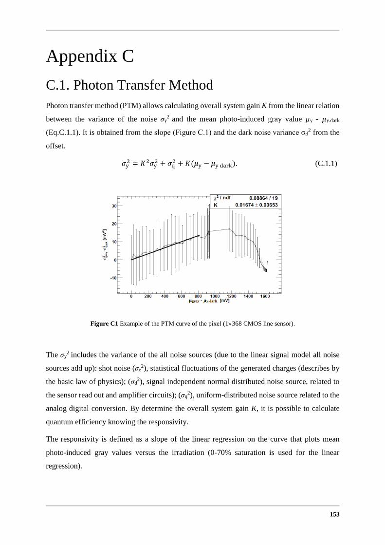
153
Appendix C
C.1. Photon Transfer Method
Photon transfer method (PTM) allows calculating overall system gain K from the linear relation
between the variance of the noise σy2 and the mean photo-induced gray value µy - µy.dark
(Eq.C.1.1). It is obtained from the slope (Figure C.1) and the dark noise variance σd2 from the
offset.
𝜎y2 = 𝐾2𝜎y
2 + 𝜎q2 + 𝐾(𝜇y − 𝜇y dark). (C.1.1)
Figure C1 Example of the PTM curve of the pixel (1368 CMOS line sensor).
The σy2 includes the variance of the all noise sources (due to the linear signal model all noise
sources add up): shot noise (σe2), statistical fluctuations of the generated charges (describes by
the basic law of physics); (σd2), signal independent normal distributed noise source, related to
the sensor read out and amplifier circuits); (σq2), uniform-distributed noise source related to the
analog digital conversion. By determine the overall system gain K, it is possible to calculate
quantum efficiency knowing the responsivity.
The responsivity is defined as a slope of the linear regression on the curve that plots mean
photo-induced gray values versus the irradiation (0-70% saturation is used for the linear
regression).
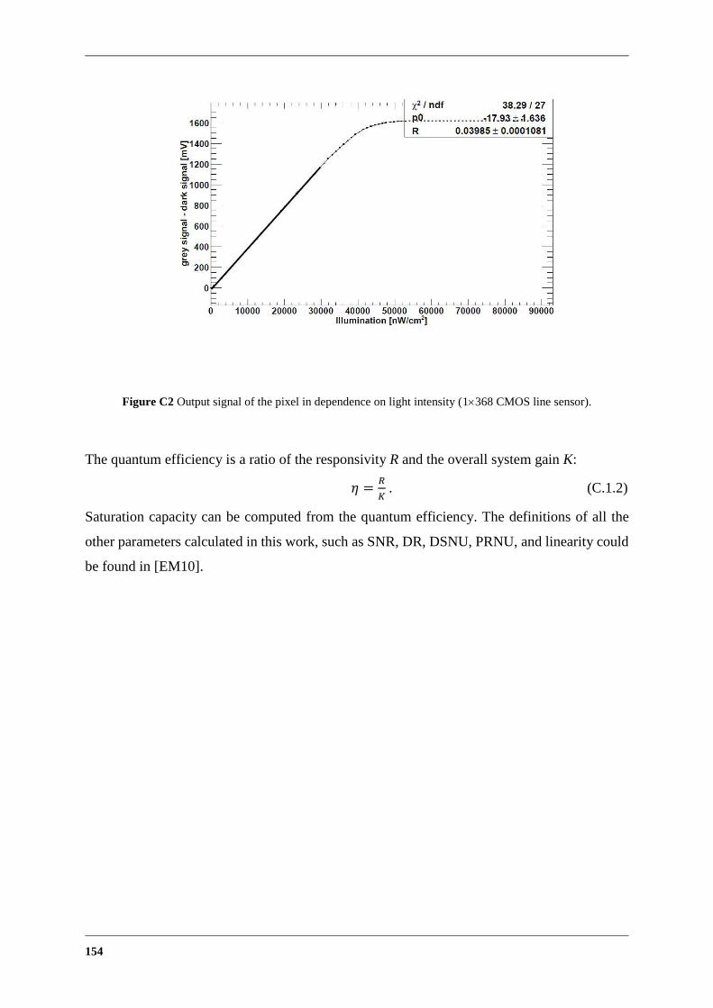
154
Figure C2 Output signal of the pixel in dependence on light intensity (1368 CMOS line sensor).
The quantum efficiency is a ratio of the responsivity R and the overall system gain K:
𝜂 =𝑅
𝐾 . (C.1.2)
Saturation capacity can be computed from the quantum efficiency. The definitions of all the
other parameters calculated in this work, such as SNR, DR, DSNU, PRNU, and linearity could
be found in [EM10].

155
Abbreviations
ADC
AES
BCCD
Analog-Digital-Konverter
Atomic Emission Spectroscopy
Buried Charge Coupled Device
CCD Charge Coupled Device
CDS Correlated Double Sampling
CG Collection Gate
CMOS
DG
DD
DOM
Complementary Metal Oxide Semiconductor
Draining Gate
Draining Diffusion
Draining-Only Modulation
DR
DRNU
Dynamic Range
Dark Response non-uniformity
FD
FPN
FF
FOX
Floating Diffusion
Fixed Pattern Noise
Fill Factor
Field Oxide
FPGA
FWC
QE
ICP
Field Programmable Gate Array
Full-well capacity
Quantum Efficiency
Inductively Coupled Plasma
LDPD
LOXOS
Lateral Drift-Field Photodiode
Local Oxidation of Silicon
MTX
MRD
MRS
MSEL
Transfer Gate Transistor
Amplifier Transistor
Reset Transistor
Select Transistor
MOS Metal Oxide Semiconductor
NMOS
NDR
NW
n-Kanal MOS-Transistor
Non-destructive Readout
n-well

156
OES
PA
Optical Emission Spectroscopy
Photoactive Area
PG Photogate
PMOS
PMT
p-channel MOSFET
Photomultiplier Tubes
PD Photodiode
PPD
PRNU
PSUB
PSN
PTM
PW
RN
Pinned Photodiode
Photo Response Non-Uniformity
p-type Substrate
Photon Shot Noise
Photon Transfer Method
p-well
Read Out Node
RST
SCR
SF
Reset
Space-Charge Region
Source Follower
SEL
SID
SN
SNR
Select
Self-Induced Drift
Sense-Node
Signal-to-Noise Ration
TCAD Technology Computer Aided Design
TG Transfer Gate
ToF
TRM
Time-of-Flight
Time-resolved Measurement
UV Ultraviolet

157
Bibliography
[Ag03] G. Agranov, V.Berezin and R.H.Tsai, “Crosstalk and Microlens Study in a
Color CMOS Image Sensor,” IEEE Transactions on Electron Devices Society,
2003.
[Ap01] Applied Photonics, “An Introduction to Laser-Induced Breakdown
Spectroscopy,” 2001.
[Ba75] D.Barbe, “Imaging Devices Using the Charge-Coupled Concept,” Proceeding of
the IEEE, vol.63, No.1, pp.38-67, 1975.
[Be05] D.Benoit et. al, “Effects of Silicon Nitride Passivation Layer on Mean Dark
Current and Quantum Efficiency of CMOS Active Pixel Sensors ,”
Mat.Res.Soc.Symp.Proc., vol.864, pp.443-448, 2005.
[Bi06] M.Bigas et. al, “Review of CMOS image sensors,” Microelectronics Journal,
vol.37, pp.433-451, 2006.
[Bla09] N.Blanc et. al, “More than Moore. Semiconductor Image Sensing,” Chapter 8,
Springer US, pp. 239-278, 2009.
[Blo10] L.Blockstein and O.Yadid-Pecht, “Crosstalk quantification, analysis, and trends
in CMOS image sensors,” Applied Optics, vol. 49, No.24, pp.4483-4488, 2010.
[Bon12] L.Bonjour et.al., “Experimental Analysis of Lag Sources in Pinned
Photodiodes,” IEEE Electron Device Letters, vol. 33,No.12, pp.1735-1737,
2012.
[Bos97] C.B.Boss and K.J.Fredeen, “Concepts, Instrumentation, and Techniques in
Inductively Coupled Plasma Optical Emission Spectrometry,” Perkin-Elmer
Corporation, 1997.

158
[Bre99] Kevin F. Brennan, “The physics of semiconductors with applications to
optoelectronic devices”, Cambridge University Press, Cambridge, 1999.
[Bro10] I.Brouk et.al, “Characterization of crosstalk between CMOS photodiodes,”
Solid State Electronics, vol. 46, pp.53-59, 2002.
[Bri72] B.Brief et.al,“The buried channel charge coupled device,” The Bell System
Technical Journal, pp.1635-1640, 1972.
[Ca71] J.Carnes et.al, “Drift-Aiding Fringing Fields in Charge-Coupled Devices“,IEEE
Journal of Solid-State Circuits, vol. 6, No.5, pp.322-326, 1971.
[Ca72] J.Carnes et.al, “Free Charge Transfer in Charge-Coupled Devices“,IEEE
Transactions on Electron Devices Society ,Vol. 19, No.6, pp.798-808, 1972.
[Ch13] Y. Cheng, “Characterization of the CMOS line sensor based on lateral drift-
field photodetector (LDPD) by means of the charge transfer time
measurements”, Bachelor Thesis, University of Duisburg-Essen, 2013.
[Dun09] F.Dunnivant and J.Ginsbach, “Flame Atomic Absorbance and Emission
Spectroscopy and Inductevely Coupled Spectrometry-Mass Spectrometery”,
Whitman College, 2009.
[Dur11] D.Durini et.al, “Experimental Comparison of Four Different CMOS Pixel
Architectures Used in Indirect Time-of-Flight Distance Measurement Sensors,”
Image Sensor Workshop, 2011.
[Dur10] D.Durini et.al, “Lateral drift-field photodiode for low noise, high-speed, large
photoactive-area CMOS imaging applications,” Nuclear Instruments and
Methods in Physics Research A, vol. 624, pp.470-475, 2010.
[Dur09] D.Durini , “Solid State Imaging in Standard CMOS Processes,” Dissertation,
Duisburg-Essen University, 2009.
159
[Dur13] D.Durini, W.Brockherde and B.Hosticka, “Detector for detecting
electromagnetic radiation with transfer gate and draining gate,” U.S. Patent 0
1340299 A1, 2013.
[EM10] EMVA Standard 1288, Standard for characterization of Image sensor and
cameras, release 3.0, issued by European machine vision association,
November 29, 2010.
[En70] W.E. Engler et.al. “Surface charge transport in silicon,” Applied physics letters,
vol. 17, Num. 11, pp.469-472, 1970.
[Fi03] K. M. Findlater et al., “Source follower noise limitations in CMOS active pixel
sensors, “Proc. 2003 IEEE Workshop on CCDs and Adv. Image Sensors, 2003.
[Fo13] E. R.Fossum and D.B.Hondongwa, “A review of the Pinned Photodiode for
CCD and CMOS image sensor,” IEEE J.Electron Devices Society, pp.33-43,
2013.
[Fu01] M.Furumiya et.al, “High sensitivity and No-Crosstalk Pixel Technology for
Embedded CMOS image Sensor,” IEEE Transactions on Electron Devices,
pp. 2221 – 2227, 2001.
[Gu97] R.M.Guidash et.al, “A 0.6 μm CMOS pinned photodiode color image
technology,” in Proc.IEDM, pp.927-929, December 1997.
[Ha06] S-W. Han, “Low dark current CMOS image sensor pixel with photodiode
structure enclosed by p-well”, Electronics Letters, Vol.42, No.20, 2006.
[Ha07] H. Han et.al, “Evaluation of a small negative bias on the performance of 4T
CMOS image sensor pixels”, in Proc. Int. Image Sensor Workshop, pp.238-240,
2007.

160
[Ha05] S-W. Han rt.al, “A Low dark current CMOS image sensor pixel with photodiode
structure enclosed by p-well”, Journal of semiconductor technology and science,
Vol.5, No.2, 2005.
[Ho13] F. Hochschulz, “CMOS-Back-End-of-Line-Prozesse für optische Bauelemente”,
Dissertation, University of Duisburg-Essen, 2013.
[Hs04] T. Hsu, “The mechanism and Evaluation of Hot-Carrier-Induced Performance
Degradation in 0.18-µm CMOS Image Sensor”, IEEE Electron Device Letters,
Vol.25, No.6, 2004.
[Hs05] T. Hsu, “A High-Efficiency CMOS image Sensor With Air Gap in situ MicroLens
(AGML) Fabricated by 0.18-µm CMOS Technology”, IEEE Electron Device
Letters, Vol.26, No.9, 2005.
[In03] I. Inoue, “Low-Leakage-Current and Low-Operating- Voltage Buried
Photodiode for a CMOS Imager,” IEEE Transactions on Electron Devices,
Vol.50, No.1., 2003.
[Jan05] J. Janesick, “Photon Transfer DN→λ”, SPIE press, 2007.
[Jar01] R. Jarwal, D.Misra and J.Lowrance, “Charge Transfer in a Multi-Implant
Pinned-Buried Photodetector,” IEEE Transactions on Electron Devices, Vol.48,
No.5., 2001.
[Ju13] J.H.Jungmann,“Detection systems for mass spectrometry imaging; A
perspective on novel developments with a focus on active pixel detectors”,
Rapid. Commun. Mass.Spectrom.,vol.27,pp..1-23, 2013.
[Ob] www.oblf.de
[Ki71] Choonfg-Ki Kim and Martin Lenzlinger, “Charge Transfer in Charge-Coupled
Devices”, Journal of Applied Physics, Vol.42, 1971.
161
[Ko96] W. Kosonocky, “360 x 360 element very-high frame-rate burst-image sensor”,
1996 Intl. Solid-State Circuits Conf. (ISSCC) Dig. of Technical Papers, pp.182-
183, 1996.
[Ko97] W.Kosonocky, “360 x 360 element three-phase very high frame rate burst image
sensor: design, operation and performance”, IEEE Transactions on Electron
Devices, Vol.44, No.10, 1997.
[Kw97] H. Kwon et.al., “The analysis of Dark Signals in the CMOS APS Imagers From
the Characterization of Test Structures”, IEEE Transactions on Electron
Devices, Vol.51, No.2, 2004.
[Li12] Zhuo Li et.al., “A Time-Resolved CMOS Image Sensor With Draining-Only
Modulation Pixels for Fluorescence Lifetime Imaging”, IEEE Transactions on
Electron Devices, Vol.59, No.10, 2012.
[Lo03] N.Loukianova et.al., “Leakage Current Modeling of Test Structures for
Characterization of Dark Current in CMOS Image Sensors”, IEEE Transactions
on Electron Devices, Vol.50, No.1, 2003.
[Mae03] S.Maestre and P.Magnan, “Electroluminescence and Impact Ionization in
CMOS Active Pixel Sensors”, Proceedings of the IISW, 2003.
[Mah10] R.Mahdi et.al. , “Lateral Drift-Field Photodetector for high speed 0.35 µm
CMOS imaging sensors based on non-uniform lateral doping profile: Design,
theoretical concepts and TCAD simulations”, Conference on Ph.D. Research in
Microelectronics and Electronics (PRIME), pp.1-4, 2010.
[Mh08] B.Mheen et.al. , “Negative offset operation of four-transistor CMOS image
pixels for increased well capacity and suppressed dark current”, IEEE Electron
Device Lett., vol.29, no.4, pp.347-349, 2008.
[Na05] J.Nakamura, “Image sensors and signal processing for digital still cameras”,
Taylor & Francis Group, 2005.

162
[Oh08] J.Ohta,“Smart CMOS image sensor and applications”, Taylor & Francis Group,
2008.
[Pa06] G.Patounakis et.al.,“Active CMOS Array Sensor for Time-Resolved
Fluorescence Detection”, IEEE Journal of Solid-State Circuits,
vol.41,No.11,pp..2521-2530, 2006.
[Po13] E.Poklonskaya,“Line sensor for fast, time-resolved spectroscopy
measurements”, Presented at AMA conference, Available: http://ama-
science.org/ama-conferences-2013/
[Ra07] P.Rao et.al,"Radiation Hardness of Deep-Submicron CMOS Technology
Evaluated by Gated-Diode Measurements," Sense of Contact, Zeist, the
Netherlands, (2007).
[Re10] J.Regolini et.al.,“Passivation issues in active pixel CMOS image sensors”,
Microelectronics Reliability 47, pp.739-742, 2007.
[Sa80] N.Saks, “A technique for suppressing dark current generated by interface states
in buried channel CCD Imagers”, IEEE Electron Device Letters, vol.EDL-1,
No.7, July,1980.
[Si10] B.Shin,“The effect of photodiode shape on charge transfer in CMOS image
sensors”, Solid State Electronics 54, pp.1416-1420, 2010.
[Sp11] A.Spickermann, “CMOS 3D Image sensor based on pulse modulated Time-of-
Flight principle and intrinsic lateral Drift-Field Photodiode Pixels”,
Proceedings of the ESSCIRC, pp.111-114, 2011.
[Sua08] Suat Utku Ay, “Large format CMOS image sensors“, VDM Verlag Dr. Müller,
2008.
[Sus13] A. Suss, “Speed considerations for LDPD based time-of-flight CMOS 3D image
sensors”, Proceedings of the ESSCIRC, pp.292-302, 2013.
163
[Sz07] S.M. Sze, “Physics of semiconductor devices“, Third edition, A John Wiley &
Sons, Inc., Publication, 2007.
[Sy13] Synopsys TCAD simulation tool, 2013
[The95] A.Theuwissen, “Solid-State Imaging with Charge-Coupled Devices,” Kluwer
Academic Publishers, 1995.
[The01] A.Theuwissen, “CCD or CMOS image sensors for consumer digital still
photography?“ ,in International Symposium on VLSI Technology, Systems, and
Applications, 2001. Proceedings of Technical Papers, 2001, pp. 168–171.
[The06] A.Theuwissen, “The Hole Role in Solid-State Imagers”, IEEE Transactions on
Electron Devices, Vol.53, No.12, 2006.
[Tho96] V. B.E. Thomsen, “Modern Spectrochemical Analysis of Metals“, OH:
ASM International, 1996, pp. 62–65.
[Tu09] C.Tubert et.al., “High speed dual port pinned-photodiode for Time-of-Flight
imaging”, Proc. 2009 Intl.Image Sensor Workshop (IISW), 2009.
[Wa01] C.Wang and C.G.Sodini, “A Crosstalk Study of CMOS Active Pixel Sensor
Arrays for Color Imager Application, “Proc. 2001 IEEE Workshop on CCDs
and Adv. Image Sensors, 2001.
[Wa08] X.Wang et.al., “A CMOS image sensor with a buried-channel source follower,
“ISSCC Tech. Dig, 62-63,2008.
[Wo97] H.-S.P. Wong, “Cmos image sensors-recent advances and device scaling
considerations, “ International Electron Devices Meeting 1997. IEDM, 1997,
pp. 201–204.
164
[Xi00] X.Hou and B.T.Jones, “Inductively Coupled Plasma/Optical Emission
Spectrometry,” Encyclopedia of Analytical Chemistry, R.A.Meyers (Ed.),
pp.9468-9485, 2000.
[Yad04] O.Yadid-Pecht and R.Etienne-Cummings, “CMOS imagers: from
phototransduction to image processing,” Kluwer Academic Publishers, 2004.
[Yan04] G. Yang and Loc Truong, “Implement Multiple Pixel Output for Photodiode Size
Pixels,” U.S. Patent 20140027609 A1, 2014.
[Yon03] R.A.Yonemoto et.al.,, “A CMOS image sensor with a simple FPN-reduction
technology and a hole accumulated diode,” in Proc.ISSCC, pp.102-103, 2000.
[Yot03] R.A.Yotter, “A review of Photodetectors for Sensing Light-Emitting Reporters
in Biological Systems,” IEEE Sensors Journal, vol. 3, No.3, pp.288-303, 2003.
[Li12] Zhuo Li et.al.,, “A Time-Resolved CMOS Image Sensor with Draining-Only
Modulation Pixels for Fluorescence Lifetime Imaging,” IEEE Transactions on
Electron Devices, Vol.59, No.10, 2012.


