LAN950x USB 2.0 to 10/100 Ethernet Controller - Data Sheet
213
2010-2021 Microchip Technology Inc. DS00001875D-page 1 Highlights • Single Chip Hi-Speed USB 2.0 to 10/100 Ethernet Controller • Integrated 10/100 Ethernet MAC with Full-Duplex Support • Integrated 10/100 Ethernet PHY with HP Auto- MDIX support • Integrated USB 2.0 Hi-Speed Device Controller • Integrated USB 2.0 Hi-Speed PHY • Implements Reduced Power Operating Modes Target Applications • Embedded Systems • Set-Top Boxes • PVRs • CE Devices • Networked Printers • USB Port Replicators • Standalone USB to Ethernet Dongles • Test Instrumentation • Industrial Key Features • USB Device Controller - Fully compliant with Hi-Speed Universal Serial Bus Specification Revision 2.0 - Supports HS (480 Mbps) and FS (12 Mbps) modes - Four endpoints supported - Supports vendor specific commands - Integrated USB 2.0 PHY - Remote wakeup supported • High-Performance 10/100 Ethernet Controller - Fully compliant with IEEE802.3/802.3u - Integrated Ethernet MAC and PHY - 10BASE-T and 100BASE-TX support - Full- and half-duplex support - Full- and half-duplex flow control - Preamble generation and removal - Automatic 32-bit CRC generation and check- ing - Automatic payload padding and pad removal - Loop-back modes - TCP/UDP/IP/ICMP checksum offload support - Flexible address filtering modes –One 48-bit perfect address –64 hash-filtered multicast addresses –Pass all multicast –Promiscuous mode –Inverse filtering –Pass all incoming with status report - Wakeup packet support - Integrated Ethernet PHY –Auto-negotiation –Automatic polarity detection and correction –HP Auto-MDIX support –Link status change wake-up detection - Support for 3 status LEDs - External MII and Turbo MII support Home- PNA™ and HomePlug® PHY • Power and I/Os - Various low power modes - NetDetach feature increases battery life 1 - Supports PCI-like PME wake 1 - 11 GPIOs - Supports bus-powered and self-powered operation - Integrated power-on reset circuit - Single external 3.3v I/O supply –Internal core regulator • Miscellaneous Features - EEPROM Controller - Supports custom operation without EEPROM 1 - IEEE 1149.1 (JTAG) Boundary Scan - Requires single 25 MHz crystal • Software - Windows XP/Vista Driver - Linux Driver - Win CE Driver - MAC OS Driver - EEPROM Utility • Packaging - 56-pin QFN (8x8 mm) RoHS Compliant Environmental - Commercial Temperature Range (0°C to +70°C) - Industrial Temperature Range (-40°C to +85°C) 1 = LAN9500A/LAN9500Ai ONLY LAN9500/LAN9500i/LAN9500A/LAN9500Ai LAN950x USB 2.0 to 10/100 Ethernet Controller
Transcript of LAN950x USB 2.0 to 10/100 Ethernet Controller - Data Sheet

LAN9500/LAN9500i/LAN9500A/LAN9500Ai
LAN950x USB 2.0 to 10/100 Ethernet Controller
Highlights
• Single Chip Hi-Speed USB 2.0 to 10/100 Ethernet Controller
• Integrated 10/100 Ethernet MAC with Full-Duplex Support
• Integrated 10/100 Ethernet PHY with HP Auto-MDIX support
• Integrated USB 2.0 Hi-Speed Device Controller
• Integrated USB 2.0 Hi-Speed PHY
• Implements Reduced Power Operating Modes
Target Applications
• Embedded Systems
• Set-Top Boxes
• PVRs
• CE Devices
• Networked Printers
• USB Port Replicators
• Standalone USB to Ethernet Dongles
• Test Instrumentation
• Industrial
Key Features
• USB Device Controller
- Fully compliant with Hi-Speed Universal Serial Bus Specification Revision 2.0
- Supports HS (480 Mbps) and FS (12 Mbps) modes
- Four endpoints supported- Supports vendor specific commands- Integrated USB 2.0 PHY- Remote wakeup supported
• High-Performance 10/100 Ethernet Controller
- Fully compliant with IEEE802.3/802.3u- Integrated Ethernet MAC and PHY- 10BASE-T and 100BASE-TX support- Full- and half-duplex support- Full- and half-duplex flow control- Preamble generation and removal- Automatic 32-bit CRC generation and check-
ing- Automatic payload padding and pad removal- Loop-back modes- TCP/UDP/IP/ICMP checksum offload support
- Flexible address filtering modes–One 48-bit perfect address–64 hash-filtered multicast addresses–Pass all multicast–Promiscuous mode–Inverse filtering–Pass all incoming with status report
- Wakeup packet support- Integrated Ethernet PHY
–Auto-negotiation–Automatic polarity detection and correction–HP Auto-MDIX support–Link status change wake-up detection
- Support for 3 status LEDs- External MII and Turbo MII support Home-
PNA™ and HomePlug® PHY
• Power and I/Os
- Various low power modes- NetDetach feature increases battery life1
- Supports PCI-like PME wake1
- 11 GPIOs- Supports bus-powered and self-powered
operation- Integrated power-on reset circuit- Single external 3.3v I/O supply
–Internal core regulator
• Miscellaneous Features
- EEPROM Controller- Supports custom operation without
EEPROM1
- IEEE 1149.1 (JTAG) Boundary Scan- Requires single 25 MHz crystal
• Software
- Windows XP/Vista Driver- Linux Driver- Win CE Driver- MAC OS Driver- EEPROM Utility
• Packaging
- 56-pin QFN (8x8 mm) RoHS Compliant
Environmental
- Commercial Temperature Range (0°C to +70°C)
- Industrial Temperature Range (-40°C to +85°C)
1 = LAN9500A/LAN9500Ai ONLY
2010-2021 Microchip Technology Inc. DS00001875D-page 1
LAN950x
TO OUR VALUED CUSTOMERS
It is our intention to provide our valued customers with the best documentation possible to ensure successful use of your Microchipproducts. To this end, we will continue to improve our publications to better suit your needs. Our publications will be refined andenhanced as new volumes and updates are introduced.
If you have any questions or comments regarding this publication, please contact the Marketing Communications Department viaE-mail at [email protected]. We welcome your feedback.
Most Current Data SheetTo obtain the most up-to-date version of this data sheet, please register at our Worldwide Web site at:
http://www.microchip.com
You can determine the version of a data sheet by examining its literature number found on the bottom outside corner of any page. The last character of the literature number is the version number, (e.g., DS30000000A is version A of document DS30000000).
ErrataAn errata sheet, describing minor operational differences from the data sheet and recommended workarounds, may exist for cur-rent devices. As device/documentation issues become known to us, we will publish an errata sheet. The errata will specify therevision of silicon and revision of document to which it applies.
To determine if an errata sheet exists for a particular device, please check with one of the following:• Microchip’s Worldwide Web site; http://www.microchip.com• Your local Microchip sales office (see last page)
When contacting a sales office, please specify which device, revision of silicon and data sheet (include -literature number) you areusing.
Customer Notification SystemRegister on our web site at www.microchip.com to receive the most current information on all of our products.
DS00001875D-page 2 2010-2021 Microchip Technology Inc.
2010-2021 Microchip Technology Inc. DS00001875D-page 3
LAN950x
Table of Contents
1.0 LAN950x Family Differences Overview .......................................................................................................................................... 42.0 Introduction ..................................................................................................................................................................................... 63.0 Pin Description and Configuration ................................................................................................................................................ 114.0 Power Connections ....................................................................................................................................................................... 245.0 Functional Description .................................................................................................................................................................. 256.0 PME Operation ........................................................................................................................................................................... 1127.0 Register Descriptions .................................................................................................................................................................. 1168.0 Operational Characteristics ......................................................................................................................................................... 1899.0 Package Outline .......................................................................................................................................................................... 207Appendix A: Data Sheet Revision History ......................................................................................................................................... 209The Microchip Web Site .................................................................................................................................................................... 210Customer Change Notification Service ............................................................................................................................................. 210Customer Support ............................................................................................................................................................................. 210Product Identification System ........................................................................................................................................................... 211
LAN950x
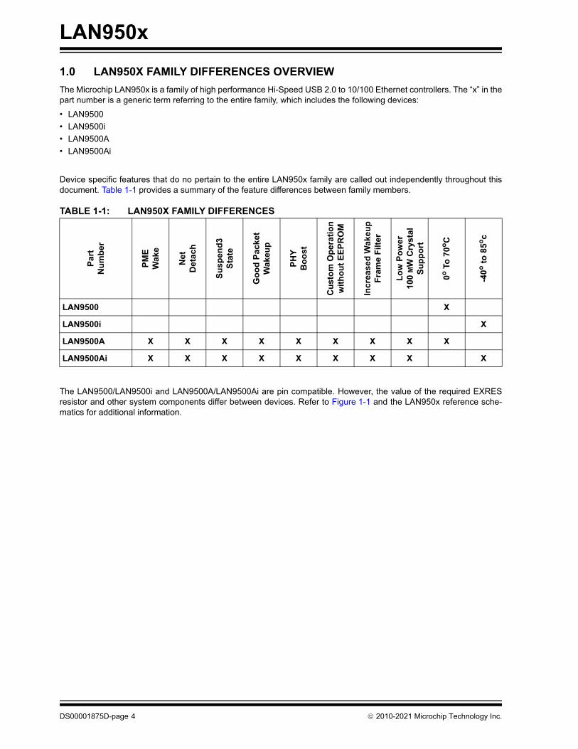
1.0 LAN950X FAMILY DIFFERENCES OVERVIEW
The Microchip LAN950x is a family of high performance Hi-Speed USB 2.0 to 10/100 Ethernet controllers. The “x” in thepart number is a generic term referring to the entire family, which includes the following devices:
• LAN9500
• LAN9500i
• LAN9500A
• LAN9500Ai
Device specific features that do no pertain to the entire LAN950x family are called out independently throughout thisdocument. Table 1-1 provides a summary of the feature differences between family members.
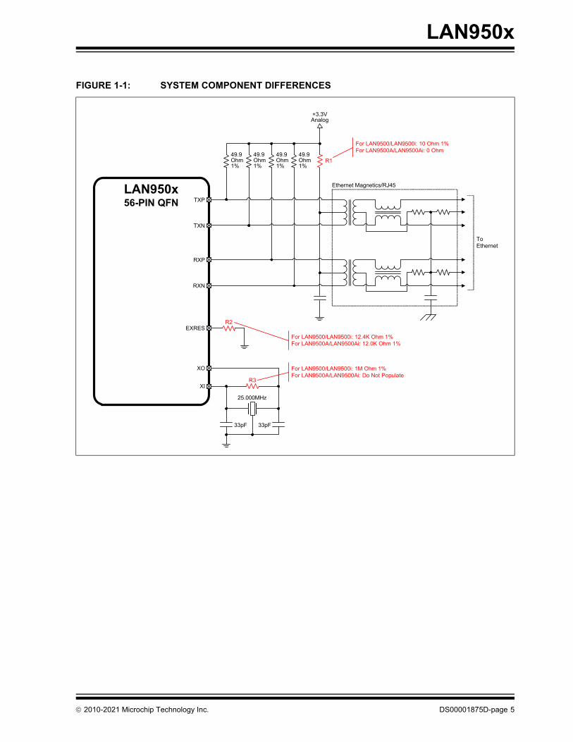
The LAN9500/LAN9500i and LAN9500A/LAN9500Ai are pin compatible. However, the value of the required EXRESresistor and other system components differ between devices. Refer to Figure 1-1 and the LAN950x reference sche-matics for additional information.
TABLE 1-1: LAN950X FAMILY DIFFERENCES
Par
t N
um
ber
PM
EW
ake
Ne
tD
eta
ch
Su
spen
d3
Sta
te
Go
od
Pac
ket
Wa
keu
p
PH
Y
Bo
ost
Cu
sto
m O
per
ati
on
wit
ho
ut
EE
PR
OM
Incr
ease
d W
ake
up
Fra
me
Filt
er
Lo
w P
ow
er10
0Μ
W C
ryst
alS
up
po
rt
0o T
o 7
0oC
-40
o t
o 8
5oc
LAN9500 X
LAN9500i X
LAN9500A X X X X X X X X X
LAN9500Ai X X X X X X X X X
DS00001875D-page 4 2010-2021 Microchip Technology Inc.
LAN950x
FIGURE 1-1: SYSTEM COMPONENT DIFFERENCES
+3.3V Analog
LAN950x56-PIN QFN TXP
TXN
RXP
RXN
R1
For LAN9500/LAN9500i: 10 Ohm 1%For LAN9500A/LAN9500Ai: 0 Ohm
Ethernet Magnetics/RJ45
To Ethernet
49.9Ohm 1%
49.9Ohm 1%
49.9Ohm 1%
49.9Ohm 1%
EXRESR2
For LAN9500/LAN9500i: 12.4K Ohm 1%For LAN9500A/LAN9500Ai: 12.0K Ohm 1%
XO
XI
33pF 33pF
25.000MHz
R3
For LAN9500/LAN9500i: 1M Ohm 1%For LAN9500A/LAN9500Ai: Do Not Populate
2010-2021 Microchip Technology Inc. DS00001875D-page 5
LAN950x
2.0 INTRODUCTION
2.1 General Terms and Conventions
The following is a list of the general terms used in this document:
BYTE 8-bits
CSR Control and Status Registers
DWORD 32-bits
FIFO First In First Out buffer
Frame In the context of this document, a frame refers to transfers on the Ethernet interface.
FSM Finite State Machine
GPIO General Purpose I/O
HOST External system (Includes processor, application software, etc.)
Level-Triggered Sticky Bit This type of status bit is set whenever the condition that it represents is asserted. The bit remains set until the condition is no longer true, and the status bit is cleared by writing a zero.
LFSR Linear Feedback Shift Register
MAC Media Access Controller
MII Media Independent Interface
N/A Not Applicable
Packet In the context of this document, a packet refers to transfers on the USB interface.
POR Power on Reset.
RESERVED Refers to a reserved bit field or address. Unless otherwise noted, reserved bits must always be zero for write operations. Unless otherwise noted, values are not guaranteed when reading reserved bits. Unless otherwise noted, do not read or write to reserved addresses.
SCSR System Control and Status Registers
SMI Serial Management Interface
TLI Transaction Layer Interface
URX USB Bulk Out Packet Receiver
UTX USB Bulk In Packet Transmitter
WORD 16-bits
ZLP Zero Length USB Packet
DS00001875D-page 6 2010-2021 Microchip Technology Inc.
LAN950x
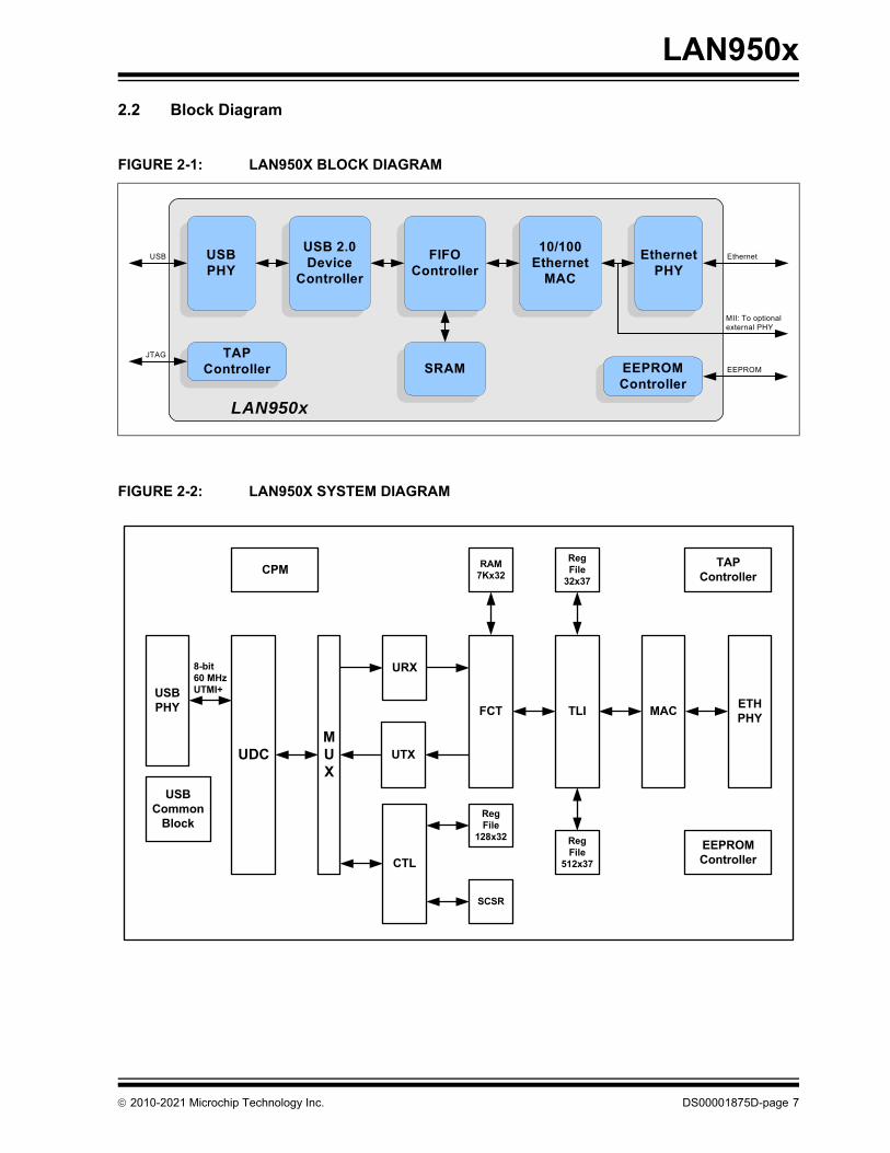
2.2 Block Diagram
FIGURE 2-1: LAN950X BLOCK DIAGRAM
FIGURE 2-2: LAN950X SYSTEM DIAGRAM
TAP Controller EEPROM
Controller
USB 2.0 Device
Controller
SRAM
EthernetPHY
10/100 Ethernet
MAC
FIFO Controller
USBPHY
LAN950x
MII: To optional external PHY
Ethernet
EEPROM
JTAG
USB
UDC
MACFCT
RAM7Kx32
TLI
RegFile
512x37
Reg File
32x37
EEPROMController
ETHPHY
USB PHY
8-bit60 MHzUTMI+
UTX
TAPController
USB Common
Block
URX
CTL
MUX
RegFile
128x32
SCSR
CPM
2010-2021 Microchip Technology Inc. DS00001875D-page 7
LAN950x
2.2.1 OVERVIEW
The LAN950x is a high performance solution for USB to 10/100 Ethernet port bridging. With applications ranging fromembedded systems, set-top boxes, and PVRs, to USB port replicators, USB to Ethernet dongles, and test instrumenta-tion, the device is targeted as a high performance, low cost USB/Ethernet connectivity solution.
The LAN950x contains an integrated 10/100 Ethernet PHY, USB PHY, Hi-Speed USB 2.0 device controller, 10/100Ethernet MAC, TAP controller, EEPROM controller, and a FIFO controller with a total of 30 KB of internal packet buffer-ing. Two KB of buffer memory are allocated to the Transaction Layer Interface (TLI), while 28 KB are allocated to theFIFO Controller (FCT).
The internal USB 2.0 device controller and USB PHY are compliant with the USB 2.0 Hi-Speed standard. The deviceimplements Control, Interrupt, Bulk-in, and Bulk-out USB Endpoints.
The Ethernet controller supports auto-negotiation, auto-polarity correction, HP Auto-MDIX, and is compliant with theIEEE 802.3 and IEEE 802.3u standards. An external MII interface provides support for an external Fast Ethernet PHY,HomePNA, and HomePlug functionality.
Multiple power management features are provided, including various low power modes and “Magic Packet”, “Wake OnLAN”, and “Link Status Change” wake events. These wake events can be programmed to initiate a USB remote wakeup.
An internal EEPROM controller exists to load various USB configuration information and the device MAC address. Theintegrated IEEE 1149.1 compliant TAP controller provides boundary scan via JTAG.
2.2.2 USB
The USB portion of LAN950x consists of the USB Device Controller (UDC), USB Bulk Out Packet Receiver (URX), USBBulk In Packet Transmitter (UTX), Control Block (CTL), System Control and Status Registers (SCSR), and USB PHY.
The USB device controller (UDC) contains a USB low-level protocol interpreter that controls the USB bus protocol,packet generation/extraction, PID/Device ID parsing, and CRC coding/decoding with autonomous error handling. It iscapable of operating either in USB 1.1 or 2.0 compliant modes. It has autonomous protocol handling functions like stallcondition clearing on setup packets, suspend/resume/reset conditions, and remote wakeup. It also autonomously han-dles contingency operations for error conditions such as retry for CRC errors, Data toggle errors, and generation ofNYET, STALL, ACK and NACK depending on the endpoint buffer status. The UDC implements four USB endpoints:Control, Interrupt, Bulk-In, and Bulk-Out.
The Control block (CTL) manages traffic to/from the control endpoint that is not handled by the UDC and constructs thepackets used by the interrupt endpoint. The CTL is responsible for handling some USB standard commands and all ven-dor specific commands. The vendor specific commands allow for efficient statistics collection and access to the SCSR.
The URX and UTX implement the bulk-out and bulk-in pipes, respectively, which connect the USB Host and the UDC.They perform the following functions:
The URX passes USB Bulk-Out packets to the FIFO Controller (FCT). It tracks whether or not a USB packet is errone-ous. It instructs the FCT to flush erroneous packets by rewinding its write pointer.
The UTX retrieves Ethernet frames from the FCT and constructs USB Bulk-In packets from them. If the handshake fora transmitted Bulk-In packet does not complete, the UTX is capable of retransmitting the packet. The UTX will notinstruct the FCT to advance its read head pointer until the current USB packet has been successfully transmitted to theUSB Host.
Both the URX and UTX are responsible for handling Ethernet frames encapsulated over USB by one of the followingmethods.
• Multiple Ethernet frames per USB Bulk packet
• Single Ethernet frame per USB Bulk packet
The UDC also implements the System Control and Status Register (SCSR) space used by the Host to obtain status andcontrol overall system operation.
The integrated USB 2.0 compliant device PHY supports high speed and full speed modes.
DS00001875D-page 8 2010-2021 Microchip Technology Inc.
LAN950x
2.2.3 FIFO CONTROLLER (FCT)
The FIFO controller uses a 28 KB internal SRAM to buffer RX and TX traffic. 20 KB is allocated for received Ethernet-USB traffic (RX buffer), while 8 KB is allocated for USB-Ethernet traffic (TX buffer). Bulk-Out packets from the USB con-troller are directly stored into the TX buffer. The FCT is responsible for extracting Ethernet frames from the USB packetdata and passing the frames to the MAC.Ethernet Frames are directly stored into the RX buffer and become the basisfor bulk-in packets. The FCT passes the stored data to the UTX in blocks typically 512 or 64 bytes in size, dependingon the current HS/FS USB operating speed.
2.2.4 ETHERNET
LAN950x integrates an IEEE 802.3 PHY for twisted pair Ethernet applications and a 10/100 Ethernet Media AccessController (MAC).
The PHY can be configured for either 100 Mbps (100Base-TX) or 10 Mbps (10Base-T) Ethernet operation in either Fullor Half Duplex configurations. The PHY block includes auto-negotiation, auto-polarity correction, and Auto-MDIX. Min-imal external components are required for the utilization of the Integrated PHY.
Optionally, an external PHY may be used via the MII (Media Independent Interface) port, effectively bypassing the inter-nal PHY. This option allows support for HomePNA and HomePlug applications.
The transmit and receive data paths within the 10/100 Ethernet MAC are independent, allowing for the highest perfor-mance possible, particularly in full-duplex mode. The Ethernet MAC operates in store and forward mode, utilizing anindependent 2KB buffer for transmitted frames, and a smaller 128 byte buffer for received frames. The Ethernet MACdata paths connect to the FIFO controller. The MAC also implements a Control and Status Register (CSR) space usedby the Host to obtain status and control its operation.
The Ethernet MAC/PHY supports numerous power management wakeup features, including “Magic Packet”, “Wake onLAN” and “Link Status Change”. Eight wakeup frame filters are provided by LAN9500A/LAN9500Ai, while four are pro-vided by LAN9500/LAN9500i.
2.2.5 TRANSACTION LAYER INTERFACE (TLI)
The TLI interfaces the MAC with the FCT. It is a conduit between these two modules through which all transmitted andreceived data, along with status information, is passed. It has separate receive and transmit data paths. The TLI containsa 2KB transmit FIFO and a 128-byte receive FIFO. The transmit FIFO operates in store and forward mode and is capa-ble of storing up to two Ethernet frames.
2.2.6 POWER MANAGEMENT
The LAN950x features four (Note 2-1) variations of USB suspend: SUSPEND0, SUSPEND1, SUSPEND2, and SUS-PEND3. These modes allow the application to select the ideal balance of remote wakeup functionality and power con-sumption.
• SUSPEND0: Supports GPIO, “Wake On LAN”, and “Magic Packet” remote wakeup events. This suspend state reduces power by stopping the clocks of the MAC and other internal modules.
• SUSPEND1: Supports GPIO and “Link Status Change” for remote wakeup events. This suspend state consumes less power than SUSPEND0.
• SUSPEND2: Supports only GPIO assertion for a remote wakeup event. This is the default suspend mode for the device.
• SUSPEND3: (Note 2-1) Supports GPIO and “Good Packet” remote wakeup event. A “Good Packet” is a received frame passing certain filtering constraints independent of those imposed on “Wake On LAN” and “Magic Packet” frames. This suspend state consumes power at a level similar to the NORMAL state, however, it allows for power savings in the Host CPU.
Note 2-1 All four SUSPEND states are supported by LAN9500A/LAN9500Ai. SUSPEND3 is not supported byLAN9500/LAN9500i.
Please refer to Section 5.12, "Wake Events," on page 100 for more information on the USB suspend states and the wakeevents supported in each state.
2010-2021 Microchip Technology Inc. DS00001875D-page 9
LAN950x
2.2.7 EEPROM CONTROLLER (EPC)
LAN950x contains an EEPROM controller for connection to an external EEPROM. This allows for the automatic loadingof static configuration data upon power-on reset, pin reset, or software reset. The EEPROM can be configured to loadUSB descriptors, USB device configuration, and MAC address.
(LAN9500A/LAN9500Ai ONLY)
2.2.8 GENERAL PURPOSE I/O
When configured for internal PHY mode, up to eleven GPIOs are supported. All GPIOs can serve as remote wakeupevents when the LAN950x is in a suspended state.
2.2.9 TAP CONTROLLER
IEEE 1149.1 compliant TAP Controller supports boundary scan and various test modes.
2.2.10 CONTROL AND STATUS REGISTERS (CSR)
LAN950x’s functions are controlled and monitored by the Host via the Control and Status Registers (CSR). This registerspace includes registers that control and monitor the USB controller, as well as elements of overall system operation(System Control and Status Registers - SCSR), the MAC (MAC Control and Status Registers - MCSR), and the PHY(accessed indirectly through the MAC via the MII_ACCESS and MII_DATA registers). The CSR may be accessed viathe USB Vendor Commands (REGISTER READ/REGISTER WRITE). Please refer to Section 5.3.3, "USB Vendor Com-mands," on page 41 for more information.
2.2.11 RESETS
LAN950x supports the following system reset events:
• Power on Reset (POR)
• Hardware Reset Input Pin Reset (nRESET)
• Lite Reset (LRST)
• Software Reset (SRST)
• USB Reset
• VBUS Reset
The device supports the following module level reset events:
• Ethernet PHY Software Reset (PHY_RST)
• nTRST Pin Reset for Tap Controller
2.2.12 TEST FEATURES
Read/Write access to internal SRAMs is provided via the CSRs. JTAG based USB BIST is available. Full internal scanand At Speed scan are supported.
2.2.13 SYSTEM SOFTWARE
LAN950x software drivers are available for the following operating systems:
• Windows XP
• Windows Vista
• Linux
• Win CE
• MAC OS
In addition, an EEPROM programming utility is available for configuring the external EEPROM.
DS00001875D-page 10 2010-2021 Microchip Technology Inc.
LAN950x
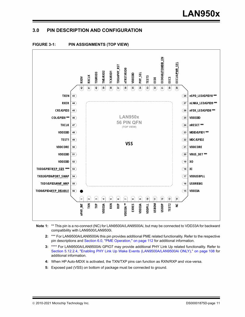
3.0 PIN DESCRIPTION AND CONFIGURATION
Note 1: ** This pin is a no-connect (NC) for LAN9500A/LAN9500Ai, but may be connected to VDD33A for backwardcompatibility with LAN9500/LAN9500i.
2: *** For LAN9500A/LAN9500Ai this pin provides additional PME related functionality. Refer to the respectivepin descriptions and Section 6.0, "PME Operation," on page 112 for additional information.
3: **** For LAN9500A/LAN9500Ai GPIO7 may provide additional PHY Link Up related functionality. Refer toSection 5.12.2.4, "Enabling PHY Link Up Wake Events (LAN9500A/LAN9500Ai ONLY)," on page 108 foradditional information.
4: When HP Auto-MDIX is activated, the TXN/TXP pins can function as RXN/RXP and vice-versa.
5: Exposed pad (VSS) on bottom of package must be connected to ground.
FIGURE 3-1: PIN ASSIGNMENTS (TOP VIEW)
VSS
LAN950x56 PIN QFN
(TOP VIEW)
TXEN
RXD
V
nSPD_LED/GPIO10 ***
NC
1 2 3 4 5 6 7 8 9 10 11 12 13 14
15
16
17
18
19
20
21
22
23
24
25
26
27
28
42 41 40 39 38 37 36 35 34 33 32 31 30 29
56
55
54
53
52
51
50
49
48
47
46
45
44
43
TEST
2
USB
DP
USB
DM
VDD
PLL
VDD
33A
EXR
ES
VDD
33A
**
RXP
RXN
VDD
33A
TXP
TXN
nPH
Y_IN
T
RXC
LK
TDI/R
XD3
TMS/
RXD
2
TCK
/RXD
1
TDO
/nPH
Y_R
ST
nTR
ST/R
XD0
VDD
33IO
PHY_
SEL
TEST
3
EED
I
EED
O/A
UTO
MD
IX_E
N
EEC
S
EEC
LK/P
WR
_SEL
RXER
CRS/GPIO3
COL/GPIO0 ***
TXCLK
VDD33IO
TEST1
VDDCORE
VDD33IO
VDD33IO
TXD3/GPIO7/EEP_SIZE ****
TXD2/GPIO6/PORT_SWAP
TXD1/GPIO5/RMT_WKP
TXD0/GPIO4/EEP_DISABLE
nLNKA_LED/GPIO9 ***
nFDX_LED/GPIO8 ***
VDD33IO
nRESET ***
MDIO/GPIO1 ***
MDC/GPIO2
VDDCORE
VBUS_DET ***
XO
XI
VDDUSBPLL
USBRBIAS
VDD33A
2010-2021 Microchip Technology Inc. DS00001875D-page 11
LAN950x
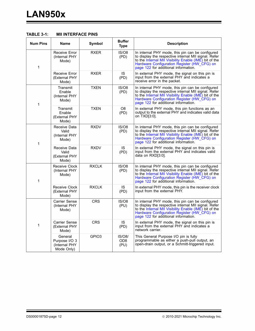
TABLE 3-1: MII INTERFACE PINS
Num Pins Name SymbolBuffer Type
Description
1
Receive Error(Internal PHY
Mode)
RXER IS/O8(PD)
In internal PHY mode, this pin can be configured to display the respective internal MII signal. Refer to the Internal MII Visibility Enable (IME) bit of the Hardware Configuration Register (HW_CFG) on page 122 for additional information.
Receive Error(External PHY
Mode)
RXER IS(PD)
In external PHY mode, the signal on this pin is input from the external PHY and indicates a receive error in the packet.
1
Transmit Enable
(Internal PHY Mode)
TXEN IS/O8(PD)
In internal PHY mode, this pin can be configured to display the respective internal MII signal. Refer to the Internal MII Visibility Enable (IME) bit of the Hardware Configuration Register (HW_CFG) on page 122 for additional information.
Transmit Enable
(External PHY Mode)
TXEN O8(PD)
In external PHY mode, this pin functions as an output to the external PHY and indicates valid data on TXD[3:0].
1
Receive Data Valid
(Internal PHY Mode)
RXDV IS/O8(PD)
In internal PHY mode, this pin can be configured to display the respective internal MII signal. Refer to the Internal MII Visibility Enable (IME) bit of the Hardware Configuration Register (HW_CFG) on page 122 for additional information.
Receive Data Valid
(External PHY Mode)
RXDV IS(PD)
In external PHY mode, the signal on this pin is input from the external PHY and indicates valid data on RXD[3:0].
1
Receive Clock(Internal PHY
Mode)
RXCLK IS/O8(PD)
In internal PHY mode, this pin can be configured to display the respective internal MII signal. Refer to the Internal MII Visibility Enable (IME) bit of the Hardware Configuration Register (HW_CFG) on page 122 for additional information.
Receive Clock(External PHY
Mode)
RXCLK IS(PD)
In external PHY mode, this pin is the receiver clock input from the external PHY.
1
Carrier Sense(Internal PHY
Mode)
CRS IS/O8(PU)
In internal PHY mode, this pin can be configured to display the respective internal MII signal. Refer to the Internal MII Visibility Enable (IME) bit of the Hardware Configuration Register (HW_CFG) on page 122 for additional information.
Carrier Sense(External PHY
Mode)
CRS IS(PD)
In external PHY mode, the signal on this pin is input from the external PHY and indicates a network carrier.
General Purpose I/O 3(Internal PHY Mode Only)
GPIO3 IS/O8/OD8(PU)
This General Purpose I/O pin is fully programmable as either a push-pull output, an open-drain output, or a Schmitt-triggered input.
DS00001875D-page 12 2010-2021 Microchip Technology Inc.
LAN950x
1
MII Collision Detect
(Internal PHY Mode)
COL IS/O8(PU)
In internal PHY mode, this pin can be configured to display the respective internal MII signal. Refer to the Internal MII Visibility Enable (IME) bit of the Hardware Configuration Register (HW_CFG) on page 122 for additional information.
MII Collision Detect
(External PHY Mode)
COL IS(PD)
In external PHY mode, the signal on this pin is input from the external PHY and indicates a collision event.
General Purpose I/O 0(Internal PHY Mode Only)
GPIO0 IS/O8/OD8(PU)
This General Purpose I/O pin is fully programmable as either a push-pull output, an open-drain output, or a Schmitt-triggered input.
Note: (LAN9500A/LAN9500Ai ONLY): This pin may be used to signal PME when Internal PHY and PME modes of operation are in effect. Refer to Section 6.0, "PME Operation," on page 112 for additional information.
1
Management Data
(Internal PHY Mode)
MDIO IS/O8(PU)
In internal PHY mode, this pin can be configured to display the respective internal MII signal. Refer to the Internal MII Visibility Enable (IME) bit of the Hardware Configuration Register (HW_CFG) on page 122 for additional information.
Management Data
(External PHY Mode)
MDIO IS/O8(PD)
In external PHY mode, this pin provides the management data to/from the external PHY.
General Purpose I/O 1(Internal PHY Mode Only)
GPIO1 IS/O8/OD8(PU)
This General Purpose I/O pin is fully programmable as either a push-pull output, an open-drain output, or a Schmitt-triggered input.
Note: (LAN9500A/LAN9500Ai ONLY): This pin may serve as the PME_MODE_SEL input when Internal PHY and PME modes of operation are in effect. Refer to Section 6.0, "PME Operation," on page 112 for additional information.
1
Management Clock
(Internal PHY Mode)
MDC IS/O8(PU)
In internal PHY mode, this pin can be configured to display the respective internal MII signal. Refer to the Internal MII Visibility Enable (IME) bit of the Hardware Configuration Register (HW_CFG) on page 122 for additional information.
Management Clock
(External PHY Mode)
MDC O8(PD)
In external PHY mode, this pin outputs the management clock to the external PHY.
General Purpose I/O 2(Internal PHY Mode Only)
GPIO2 IS/O8/OD8(PU)
This General Purpose I/O pin is fully programmable as either a push-pull output, an open-drain output, or a Schmitt-triggered input.
TABLE 3-1: MII INTERFACE PINS (CONTINUED)
Num Pins Name SymbolBuffer Type
Description
2010-2021 Microchip Technology Inc. DS00001875D-page 13
LAN950x
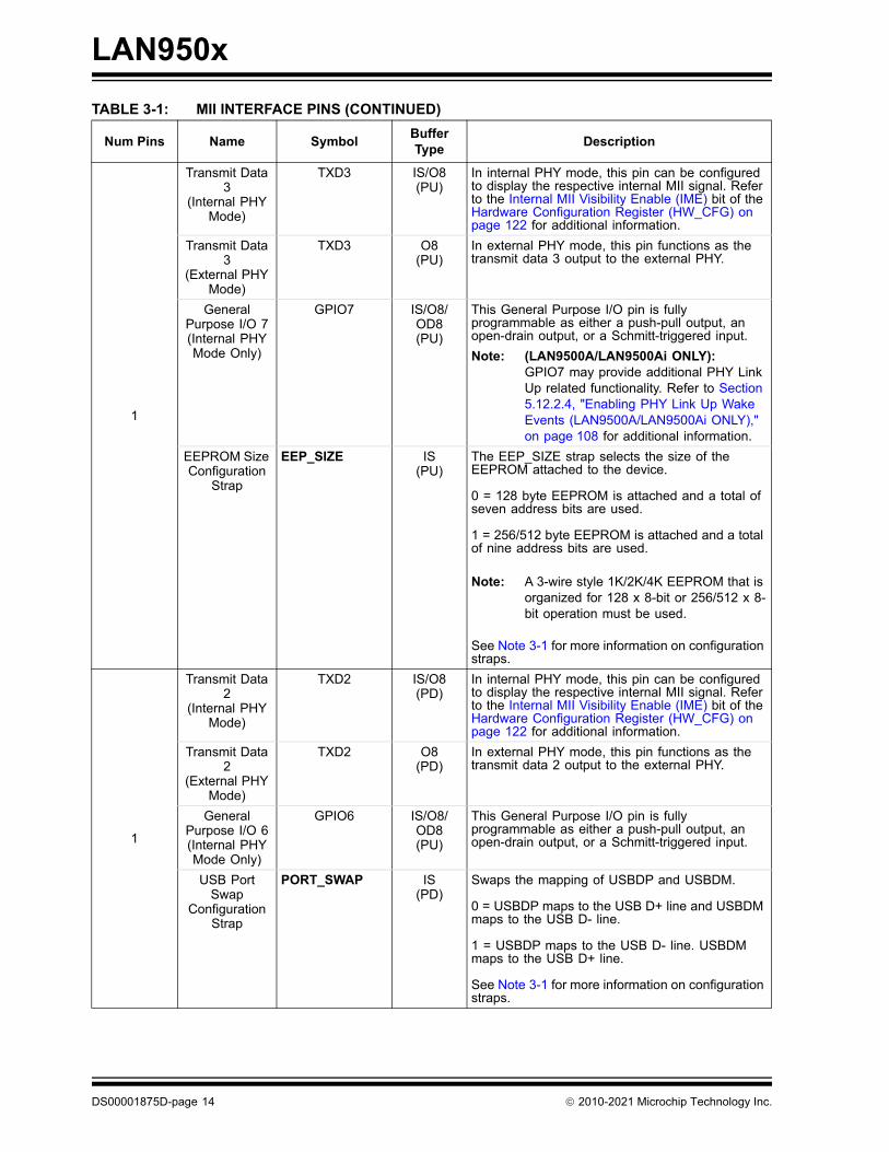
1
Transmit Data 3
(Internal PHY Mode)
TXD3 IS/O8(PU)
In internal PHY mode, this pin can be configured to display the respective internal MII signal. Refer to the Internal MII Visibility Enable (IME) bit of the Hardware Configuration Register (HW_CFG) on page 122 for additional information.
Transmit Data 3
(External PHY Mode)
TXD3 O8(PU)
In external PHY mode, this pin functions as the transmit data 3 output to the external PHY.
General Purpose I/O 7(Internal PHY Mode Only)
GPIO7 IS/O8/OD8(PU)
This General Purpose I/O pin is fully programmable as either a push-pull output, an open-drain output, or a Schmitt-triggered input.
Note: (LAN9500A/LAN9500Ai ONLY):GPIO7 may provide additional PHY Link Up related functionality. Refer to Section 5.12.2.4, "Enabling PHY Link Up Wake Events (LAN9500A/LAN9500Ai ONLY)," on page 108 for additional information.
EEPROM Size Configuration
Strap
EEP_SIZE IS(PU)
The EEP_SIZE strap selects the size of the EEPROM attached to the device.
0 = 128 byte EEPROM is attached and a total of seven address bits are used.
1 = 256/512 byte EEPROM is attached and a total of nine address bits are used.
Note: A 3-wire style 1K/2K/4K EEPROM that is organized for 128 x 8-bit or 256/512 x 8-bit operation must be used.
See Note 3-1 for more information on configuration straps.
1
Transmit Data 2
(Internal PHY Mode)
TXD2 IS/O8(PD)
In internal PHY mode, this pin can be configured to display the respective internal MII signal. Refer to the Internal MII Visibility Enable (IME) bit of the Hardware Configuration Register (HW_CFG) on page 122 for additional information.
Transmit Data 2
(External PHY Mode)
TXD2 O8(PD)
In external PHY mode, this pin functions as the transmit data 2 output to the external PHY.
General Purpose I/O 6(Internal PHY Mode Only)
GPIO6 IS/O8/OD8(PU)
This General Purpose I/O pin is fully programmable as either a push-pull output, an open-drain output, or a Schmitt-triggered input.
USB Port Swap
Configuration Strap
PORT_SWAP IS(PD)
Swaps the mapping of USBDP and USBDM.
0 = USBDP maps to the USB D+ line and USBDM maps to the USB D- line.
1 = USBDP maps to the USB D- line. USBDM maps to the USB D+ line.
See Note 3-1 for more information on configuration straps.
TABLE 3-1: MII INTERFACE PINS (CONTINUED)
Num Pins Name SymbolBuffer Type
Description
DS00001875D-page 14 2010-2021 Microchip Technology Inc.
LAN950x
Note 3-1 Configuration strap values are latched on Power-On Reset (POR) or External Chip Reset (nRESET).Configuration straps are identified by an underlined symbol name. Pins that function as configurationstraps must be augmented with an external resistor when connected to a load. Refer to Section 5.14,"Configuration Straps," on page 111 for additional information.
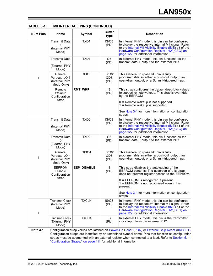
1
Transmit Data 1
(Internal PHY Mode)
TXD1 IS/O8(PD)
In internal PHY mode, this pin can be configured to display the respective internal MII signal. Refer to the Internal MII Visibility Enable (IME) bit of the Hardware Configuration Register (HW_CFG) on page 122 for additional information.
Transmit Data 1
(External PHY Mode)
TXD1 O8(PD)
In external PHY mode, this pin functions as the transmit data 1 output to the external PHY.
General Purpose I/O 5 (Internal PHY Mode Only)
GPIO5 IS/O8/OD8(PU)
This General Purpose I/O pin is fully programmable as either a push-pull output, an open-drain output, or a Schmitt-triggered input.
Remote Wakeup
Configuration Strap
RMT_WKP IS(PD)
This strap configures the default descriptor values to support remote wakeup. This strap is overridden by the EEPROM.
0 = Remote wakeup is not supported.1 = Remote wakeup is supported.
See Note 3-1 for more information on configuration straps.
1
Transmit Data 0
(Internal PHY Mode)
TXD0 IS/O8(PD)
In internal PHY mode, this pin can be configured to display the respective internal MII signal. Refer to the Internal MII Visibility Enable (IME) bit of the Hardware Configuration Register (HW_CFG) on page 122 for additional information.
Transmit Data 0
(External PHY Mode)
TXD0 O8(PD)
In external PHY mode, this pin functions as the transmit data 0 output to the external PHY.
General Purpose I/O 4 (Internal PHY Mode Only)
GPIO4 IS/O8/OD8(PU)
This General Purpose I/O pin is fully programmable as either a push-pull output, an open-drain output, or a Schmitt-triggered input.
EEPROM Disable
Configuration Strap
EEP_DISABLE IS(PD)
This strap disables the autoloading of the EEPROM contents. The assertion of this strap does not prevent register access to the EEPROM.
0 = EEPROM is recognized if present.1 = EEPROM is not recognized even if it is present.
See Note 3-1 for more information on configuration straps.
1
Transmit Clock(Internal PHY
Mode)
TXCLK IS/O8(PU)
In internal PHY mode, this pin can be configured to display the respective internal MII signal. Refer to the Internal MII Visibility Enable (IME) bit of the Hardware Configuration Register (HW_CFG) on page 122 for additional information.
Transmit Clock(External PHY
Mode)
TXCLK IS(PU)
In external PHY mode, this pin is the transmitter clock input from the external PHY.
TABLE 3-1: MII INTERFACE PINS (CONTINUED)
Num Pins Name SymbolBuffer Type
Description
2010-2021 Microchip Technology Inc. DS00001875D-page 15
LAN950x
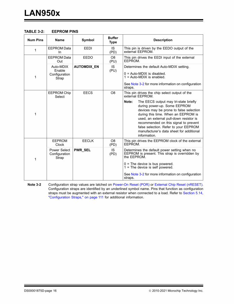
Note 3-2 Configuration strap values are latched on Power-On Reset (POR) or External Chip Reset (nRESET).Configuration straps are identified by an underlined symbol name. Pins that function as configurationstraps must be augmented with an external resistor when connected to a load. Refer to Section 5.14,"Configuration Straps," on page 111 for additional information.
TABLE 3-2: EEPROM PINS
Num Pins Name SymbolBuffer Type
Description
1 EEPROM Data In
EEDI IS(PD)
This pin is driven by the EEDO output of the external EEPROM.
1
EEPROM Data Out
EEDO O8(PU)
This pin drives the EEDI input of the external EEPROM.
Auto-MDIX Enable
Configuration Strap
AUTOMDIX_EN IS(PU)
Determines the default Auto-MDIX setting.
0 = Auto-MDIX is disabled.1 = Auto-MDIX is enabled.
See Note 3-2 for more information on configuration straps.
1
EEPROM Chip Select
EECS O8 This pin drives the chip select output of the external EEPROM.
Note: The EECS output may tri-state briefly during power-up. Some EEPROM devices may be prone to false selection during this time. When an EEPROM is used, an external pull-down resistor is recommended on this signal to prevent false selection. Refer to your EEPROM manufacturer’s data sheet for additional information.
1
EEPROM Clock
EECLK O8(PD)
This pin drives the EEPROM clock of the external EEPROM.
Power Select Configuration
Strap
PWR_SEL IS(PD)
Determines the default power setting when no EEPROM is present. This strap is overridden by the EEPROM.
0 = The device is bus powered.1 = The device is self powered.
See Note 3-2 for more information on configuration straps.
DS00001875D-page 16 2010-2021 Microchip Technology Inc.
LAN950x
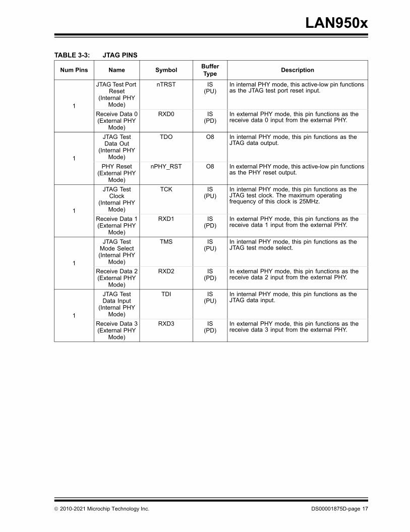
TABLE 3-3: JTAG PINS
Num Pins Name SymbolBuffer Type
Description
1
JTAG Test Port Reset
(Internal PHY Mode)
nTRST IS(PU)
In internal PHY mode, this active-low pin functions as the JTAG test port reset input.
Receive Data 0(External PHY
Mode)
RXD0 IS(PD)
In external PHY mode, this pin functions as the receive data 0 input from the external PHY.
1
JTAG Test Data Out
(Internal PHY Mode)
TDO O8 In internal PHY mode, this pin functions as the JTAG data output.
PHY Reset(External PHY
Mode)
nPHY_RST O8 In external PHY mode, this active-low pin functions as the PHY reset output.
1
JTAG Test Clock
(Internal PHY Mode)
TCK IS(PU)
In internal PHY mode, this pin functions as the JTAG test clock. The maximum operating frequency of this clock is 25MHz.
Receive Data 1(External PHY
Mode)
RXD1 IS(PD)
In external PHY mode, this pin functions as the receive data 1 input from the external PHY.
1
JTAG Test Mode Select(Internal PHY
Mode)
TMS IS(PU)
In internal PHY mode, this pin functions as the JTAG test mode select.
Receive Data 2(External PHY
Mode)
RXD2 IS(PD)
In external PHY mode, this pin functions as the receive data 2 input from the external PHY.
1
JTAG Test Data Input
(Internal PHY Mode)
TDI IS(PU)
In internal PHY mode, this pin functions as the JTAG data input.
Receive Data 3(External PHY
Mode)
RXD3 IS(PD)
In external PHY mode, this pin functions as the receive data 3 input from the external PHY.
2010-2021 Microchip Technology Inc. DS00001875D-page 17
LAN950x
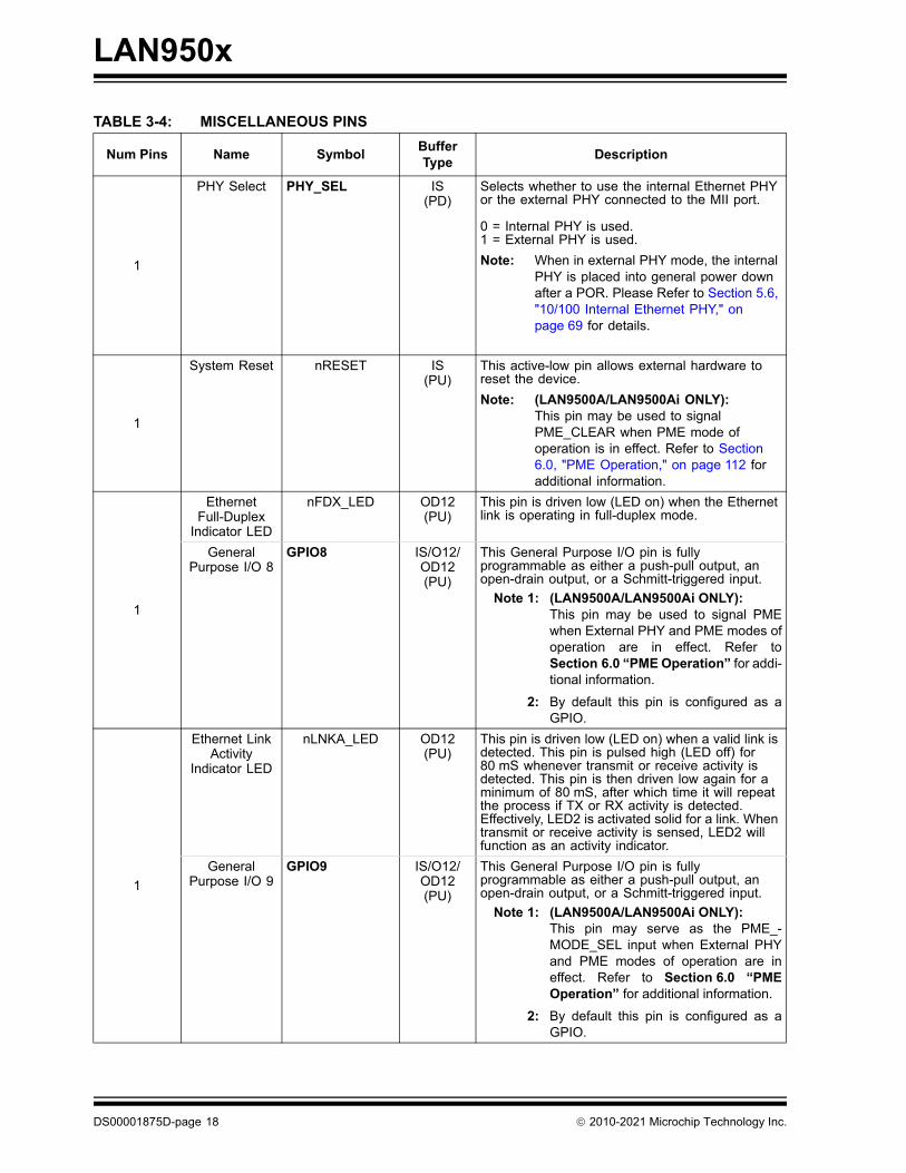
TABLE 3-4: MISCELLANEOUS PINS
Num Pins Name SymbolBuffer Type
Description
1
PHY Select PHY_SEL IS(PD)
Selects whether to use the internal Ethernet PHY or the external PHY connected to the MII port.
0 = Internal PHY is used.1 = External PHY is used.
Note: When in external PHY mode, the internal PHY is placed into general power down after a POR. Please Refer to Section 5.6, "10/100 Internal Ethernet PHY," on page 69 for details.
1
System Reset nRESET IS(PU)
This active-low pin allows external hardware to reset the device.
Note: (LAN9500A/LAN9500Ai ONLY):This pin may be used to signal PME_CLEAR when PME mode of operation is in effect. Refer to Section 6.0, "PME Operation," on page 112 for additional information.
1
Ethernet Full-Duplex
Indicator LED
nFDX_LED OD12(PU)
This pin is driven low (LED on) when the Ethernet link is operating in full-duplex mode.
General Purpose I/O 8
GPIO8 IS/O12/OD12(PU)
This General Purpose I/O pin is fully programmable as either a push-pull output, an open-drain output, or a Schmitt-triggered input.
Note 1: (LAN9500A/LAN9500Ai ONLY):This pin may be used to signal PMEwhen External PHY and PME modes ofoperation are in effect. Refer toSection 6.0 “PME Operation” for addi-tional information.
2: By default this pin is configured as aGPIO.
1
Ethernet Link Activity
Indicator LED
nLNKA_LED OD12(PU)
This pin is driven low (LED on) when a valid link is detected. This pin is pulsed high (LED off) for 80 mS whenever transmit or receive activity is detected. This pin is then driven low again for a minimum of 80 mS, after which time it will repeat the process if TX or RX activity is detected. Effectively, LED2 is activated solid for a link. When transmit or receive activity is sensed, LED2 will function as an activity indicator.
General Purpose I/O 9
GPIO9 IS/O12/OD12(PU)
This General Purpose I/O pin is fully programmable as either a push-pull output, an open-drain output, or a Schmitt-triggered input.
Note 1: (LAN9500A/LAN9500Ai ONLY):This pin may serve as the PME_-MODE_SEL input when External PHYand PME modes of operation are ineffect. Refer to Section 6.0 “PMEOperation” for additional information.
2: By default this pin is configured as aGPIO.
DS00001875D-page 18 2010-2021 Microchip Technology Inc.
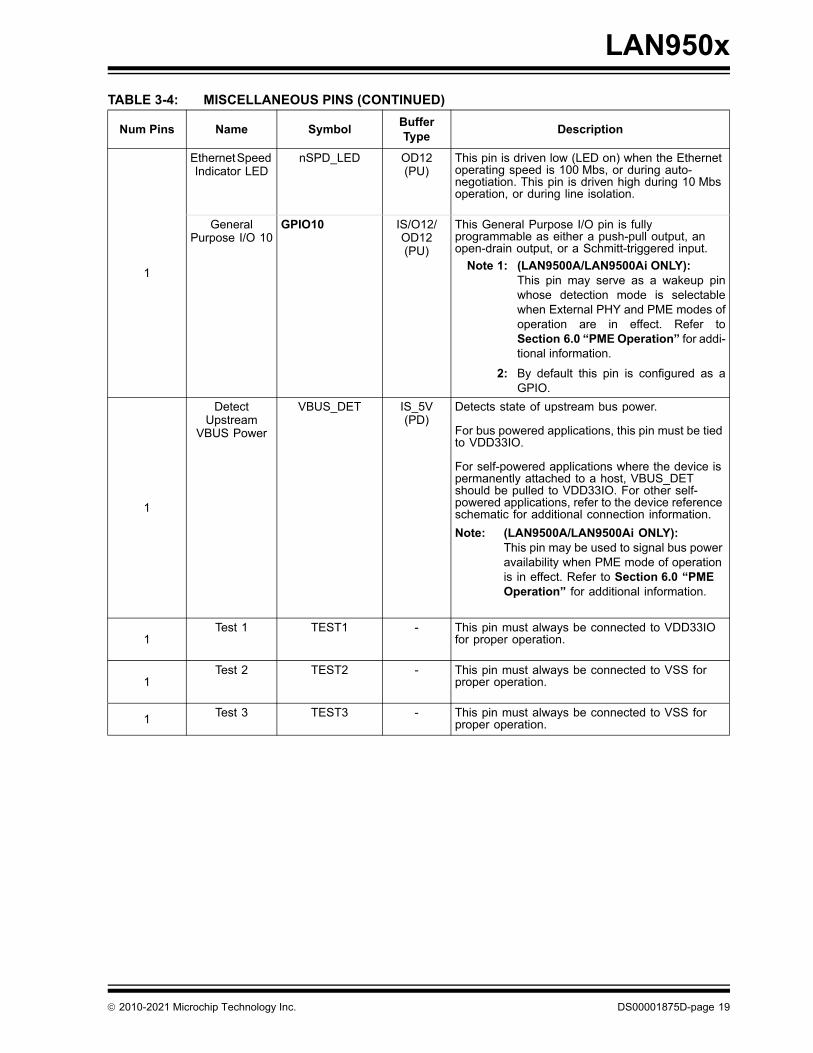
LAN950x
1
Ethernet Speed Indicator LED
nSPD_LED OD12(PU)
This pin is driven low (LED on) when the Ethernet operating speed is 100 Mbs, or during auto-negotiation. This pin is driven high during 10 Mbs operation, or during line isolation.
General Purpose I/O 10
GPIO10 IS/O12/OD12(PU)
This General Purpose I/O pin is fully programmable as either a push-pull output, an open-drain output, or a Schmitt-triggered input.
Note 1: (LAN9500A/LAN9500Ai ONLY):This pin may serve as a wakeup pinwhose detection mode is selectablewhen External PHY and PME modes ofoperation are in effect. Refer toSection 6.0 “PME Operation” for addi-tional information.
2: By default this pin is configured as aGPIO.
1
Detect Upstream
VBUS Power
VBUS_DET IS_5V(PD)
Detects state of upstream bus power.
For bus powered applications, this pin must be tied to VDD33IO.
For self-powered applications where the device is permanently attached to a host, VBUS_DET should be pulled to VDD33IO. For other self-powered applications, refer to the device reference schematic for additional connection information.
Note: (LAN9500A/LAN9500Ai ONLY):This pin may be used to signal bus power availability when PME mode of operation is in effect. Refer to Section 6.0 “PME Operation” for additional information.
1Test 1 TEST1 - This pin must always be connected to VDD33IO
for proper operation.
1Test 2 TEST2 - This pin must always be connected to VSS for
proper operation.
1Test 3 TEST3 - This pin must always be connected to VSS for
proper operation.
TABLE 3-4: MISCELLANEOUS PINS (CONTINUED)
Num Pins Name SymbolBuffer Type
Description
2010-2021 Microchip Technology Inc. DS00001875D-page 19
LAN950x
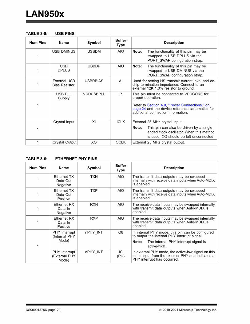
TABLE 3-5: USB PINS
Num Pins Name SymbolBuffer Type
Description
1USB DMINUS USBDM AIO Note: The functionality of this pin may be
swapped to USB DPLUS via the PORT_SWAP configuration strap.
1USB
DPLUSUSBDP AIO Note: The functionality of this pin may be
swapped to USB DMINUS via the PORT_SWAP configuration strap.
1External USB Bias Resistor.
USBRBIAS AI Used for setting HS transmit current level and on-chip termination impedance. Connect to an external 12K 1.0% resistor to ground.
1
USB PLL Supply
VDDUSBPLL P This pin must be connected to VDDCORE for proper operation.
Refer to Section 4.0, "Power Connections," on page 24 and the device reference schematics for additional connection information.
1
Crystal Input XI ICLK External 25 MHz crystal input.
Note: This pin can also be driven by a single-ended clock oscillator. When this method is used, XO should be left unconnected
1 Crystal Output XO OCLK External 25 MHz crystal output.
TABLE 3-6: ETHERNET PHY PINS
Num Pins Name SymbolBuffer Type
Description
1Ethernet TX
Data Out Negative
TXN AIO The transmit data outputs may be swapped internally with receive data inputs when Auto-MDIX is enabled.
1Ethernet TX
Data Out Positive
TXP AIO The transmit data outputs may be swapped internally with receive data inputs when Auto-MDIX is enabled.
1Ethernet RX
Data In Negative
RXN AIO The receive data inputs may be swapped internally with transmit data outputs when Auto-MDIX is enabled.
1Ethernet RX
Data In Positive
RXP AIO The receive data inputs may be swapped internally with transmit data outputs when Auto-MDIX is enabled.
1
PHY Interrupt (Internal PHY
Mode)
nPHY_INT O8 In internal PHY mode, this pin can be configured to output the internal PHY interrupt signal.
Note: The internal PHY interrupt signal is active-high.
PHY Interrupt(External PHY
Mode)
nPHY_INT IS(PU)
In external PHY mode, the active-low signal on this pin is input from the external PHY and indicates a PHY interrupt has occurred.
DS00001875D-page 20 2010-2021 Microchip Technology Inc.
LAN950x
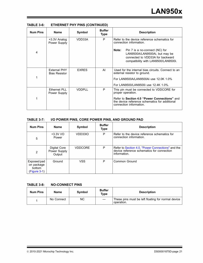
4
+3.3V Analog Power Supply
VDD33A P Refer to the device reference schematics for connection information.
Note: Pin 7 is a no-connect (NC) for LAN9500A/LAN9500Ai, but may be connected to VDD33A for backward compatibility with LAN9500/LAN9500i.
1
External PHY Bias Resistor
EXRES AI Used for the internal bias circuits. Connect to an external resistor to ground.
For LAN9500A/LAN9500Ai use 12.0K 1.0%
For LAN9500/LAN9500i use 12.4K 1.0%.
1
Ethernet PLL Power Supply
VDDPLL P This pin must be connected to VDDCORE for proper operation.
Refer to Section 4.0 “Power Connections” and the device reference schematics for additional connection information.
TABLE 3-7: I/O POWER PINS, CORE POWER PINS, AND GROUND PAD
Num Pins Name SymbolBuffer Type
Description
5
+3.3V I/O Power
VDD33IO P Refer to the device reference schematics for connection information.
2
Digital Core Power Supply
Output
VDDCORE P Refer to Section 4.0, "Power Connections" and the device reference schematics for connection information.
Exposed pad on package
bottom(Figure 3-1)
Ground VSS P Common Ground
TABLE 3-8: NO-CONNECT PINS
Num Pins Name SymbolBuffer Type
Description
1 No Connect NC — These pins must be left floating for normal device operation.
TABLE 3-6: ETHERNET PHY PINS (CONTINUED)
Num Pins Name SymbolBuffer Type
Description
2010-2021 Microchip Technology Inc. DS00001875D-page 21
LAN950x
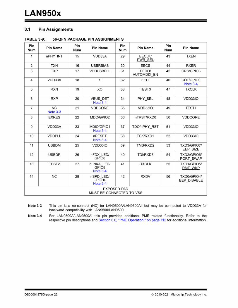
3.1 Pin Assignments
Note 3-3 This pin is a no-connect (NC) for LAN9500A/LAN9500Ai, but may be connected to VDD33A forbackward compatibility with LAN9500/LAN9500i.
Note 3-4 For LAN9500A/LAN9500Ai this pin provides additional PME related functionality. Refer to therespective pin descriptions and Section 6.0, "PME Operation," on page 112 for additional information.
TABLE 3-9: 56-QFN PACKAGE PIN ASSIGNMENTS
PinNum
Pin NamePin
NumPin Name
PinNum
Pin NamePin
NumPin Name
1 nPHY_INT 15 VDD33A 29 EECLK/PWR_SEL
43 TXEN
2 TXN 16 USBRBIAS 30 EECS 44 RXER
3 TXP 17 VDDUSBPLL 31 EEDO/AUTOMDIX_EN
45 CRS/GPIO3
4 VDD33A 18 XI 32 EEDI 46 COL/GPIO0Note 3-4
5 RXN 19 XO 33 TEST3 47 TXCLK
6 RXP 20 VBUS_DETNote 3-4
34 PHY_SEL 48 VDD33IO
7 NCNote 3-3
21 VDDCORE 35 VDD33IO 49 TEST1
8 EXRES 22 MDC/GPIO2 36 nTRST/RXD0 50 VDDCORE
9 VDD33A 23 MDIO/GPIO1Note 3-4
37 TDO/nPHY_RST 51 VDD33IO
10 VDDPLL 24 nRESETNote 3-4
38 TCK/RXD1 52 VDD33IO
11 USBDM 25 VDD33IO 39 TMS/RXD2 53 TXD3/GPIO7/EEP_SIZE
12 USBDP 26 nFDX_LED/GPIO8
40 TDI/RXD3 54 TXD2/GPIO6/PORT_SWAP
13 TEST2 27 nLNKA_LED/GPIO9
Note 3-4
41 RXCLK 55 TXD1/GPIO5/RMT_WKP
14 NC 28 nSPD_LED/GPIO10Note 3-4
42 RXDV 56 TXD0/GPIO4/EEP_DISABLE
EXPOSED PADMUST BE CONNECTED TO VSS
DS00001875D-page 22 2010-2021 Microchip Technology Inc.
LAN950x
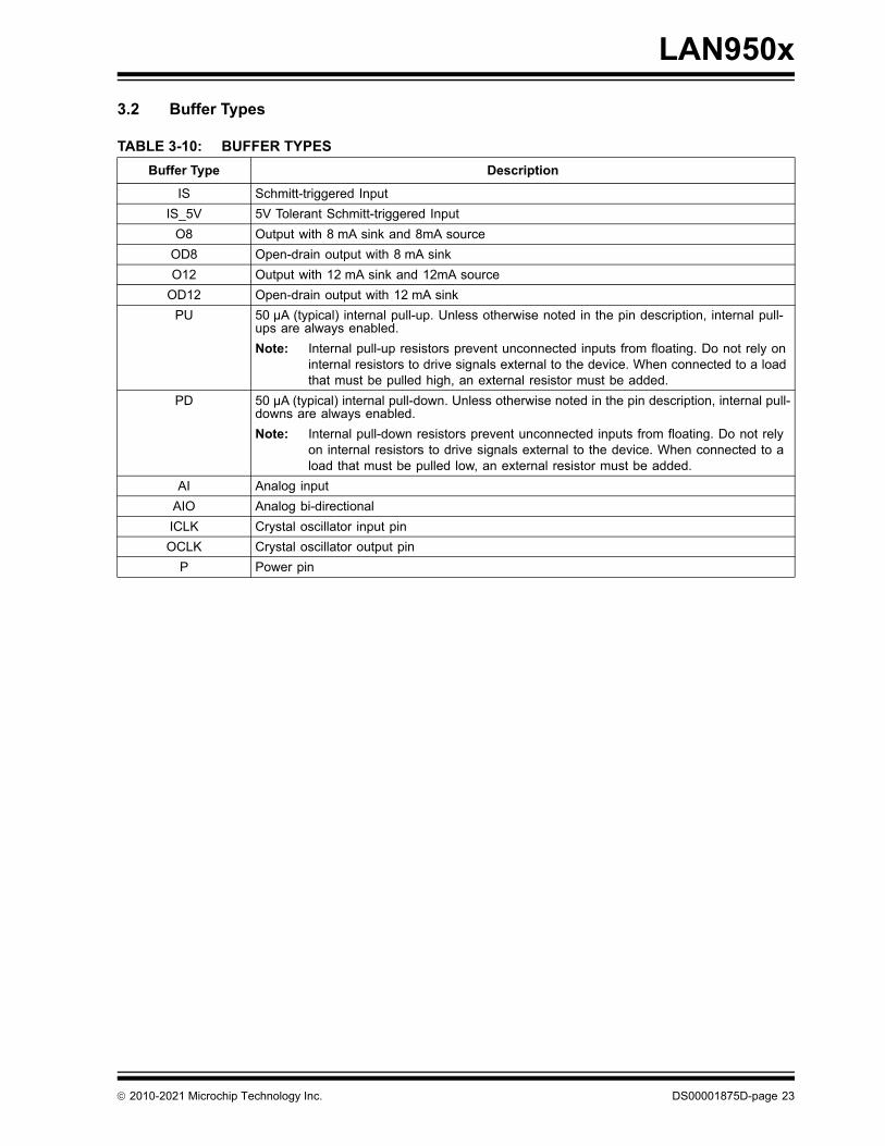
3.2 Buffer Types
TABLE 3-10: BUFFER TYPES
Buffer Type Description
IS Schmitt-triggered Input
IS_5V 5V Tolerant Schmitt-triggered Input
O8 Output with 8 mA sink and 8mA source
OD8 Open-drain output with 8 mA sink
O12 Output with 12 mA sink and 12mA source
OD12 Open-drain output with 12 mA sink
PU 50 µA (typical) internal pull-up. Unless otherwise noted in the pin description, internal pull-ups are always enabled.
Note: Internal pull-up resistors prevent unconnected inputs from floating. Do not rely on internal resistors to drive signals external to the device. When connected to a load that must be pulled high, an external resistor must be added.
PD 50 µA (typical) internal pull-down. Unless otherwise noted in the pin description, internal pull-downs are always enabled.
Note: Internal pull-down resistors prevent unconnected inputs from floating. Do not rely on internal resistors to drive signals external to the device. When connected to a load that must be pulled low, an external resistor must be added.
AI Analog input
AIO Analog bi-directional
ICLK Crystal oscillator input pin
OCLK Crystal oscillator output pin
P Power pin
2010-2021 Microchip Technology Inc. DS00001875D-page 23
LAN950x
DS00001875D-page 24 2010-2021 Microchip Technology Inc.
4.0 POWER CONNECTIONS
Figure 4-1 illustrates the power connections for LAN950x.
FIGURE 4-1: POWER CONNECTIONS
(IN) (OUT)
Internal Core Regulator
VDD33IO
+3.3V
VDDCORE
VDDCORECore Logic
1uF0.1 ohm ESR
VDDUSBPLLUSB PHY
0.1uF
Exposed Pad
VDD33A
VDD33IO
0.1uF
VDD33IO
VDD33IO
VDD33IO
0.1uF
0.1uF
0.1uF
0.1uF
0.1uF
LAN950x
VDD33A
VDD33A
VDD33A
0.1uF
0.1uF
56-PIN QFN
0.5A120 ohm @
100MHz
VSS
VDDPLL
0.1uF
PLL &
Ethernet PHY
0.5A120 ohm @
100MHz
0.1uF
0.5A120 ohm @
100MHz
LAN950x
5.0 FUNCTIONAL DESCRIPTION
5.1 Functional Overview
The LAN950x USB 2.0 to 10/100 Ethernet Controller consists of the following major functional blocks:
• USB PHY
• USB 2.0 Device Controller (UDC)
• FIFO Controller (FCT) and Associated SRAM
• 10/100 Ethernet MAC
• 10/100 Internal Ethernet PHY
• IEEE 1149.1 Tap Controller
• EEPROM Controller (EPC)
The following sections discuss the features of each block. A block diagram of the device is shown in Figure 2-1.
5.2 USB PHY
The USB PHY has the USB interface on one end, and connects to the USB 2.0 Device Controller on the other. TheParallel-to-serial/serial-to-parallel conversion, bit stuffing, and NRZI coding / decoding are handled in the PHY block.The PHY is capable of operating in the USB 1.1 and 2.0 modes.
5.3 USB 2.0 Device Controller (UDC)
The USB functionality in the device consists of five major parts. The USB PHY (discussed in Section 5.2), UCB (USBCommon Block), UDC (USB Device Controller), URX (USB Bulk Out Receiver), UTX (USB Bulk In Receiver), and CTL(USB Control Block). They are represented as the USB PHY and UDC, collectively, in Figure 2-1.
The UCB generates various clocks, including the system clocks of the device. The URX and UTX implement the BulkOut and Bulk In endpoints respectively. The CTL manages control and interrupt endpoints.
The UDC is a USB low-level protocol interpreter. The UDC controls the USB bus protocol, packet generation/extraction,PID/Device ID parsing, and CRC coding/decoding with autonomous error handling. It is capable of operating either inUSB 1.1 or 2.0 compliant modes. It has autonomous protocol handling functions like stall condition clearing on setuppackets, suspend/resume/reset conditions, and remote wakeup. It also autonomously handles error conditions such asretry for CRC errors, Data toggle errors, and generation of NYET, STALL, ACK and NACK, depending on the endpointbuffer status.
The UDC is configured to support one configuration, one interface, one alternate setting, and four endpoints.
5.3.1 SUPPORTED ENDPOINTS
Table 5-1lists the supported endpoints. The following subsections discuss these endpoints in detail.
The URX and UTX implement the Bulk Out and Bulk In endpoints, respectively. The CTL manages the Control and Inter-rupt endpoints.
5.3.1.1 Endpoint 1 (Bulk In)
The Bulk In Endpoint is controlled by the UTX (USB Bulk In Transmitter). The UTX is responsible for encapsulatingEthernet data into a USB Bulk In packet. Ethernet frames are retrieved from the FCT’s RX FIFO.
The UTX supports the following two modes of operation: MEF and SEF, selected via the Multiple Ethernet Frames perUSB Packet (MEF) bit of the Hardware Configuration Register (HW_CFG).
TABLE 5-1: SUPPORTED ENDPOINTS
EndpointNumber
Description
0 Control Endpoint
1 Bulk In Endpoint
2 Bulk Out Endpoint
3 Interrupt Endpoint
2010-2021 Microchip Technology Inc. DS00001875D-page 25
LAN950x
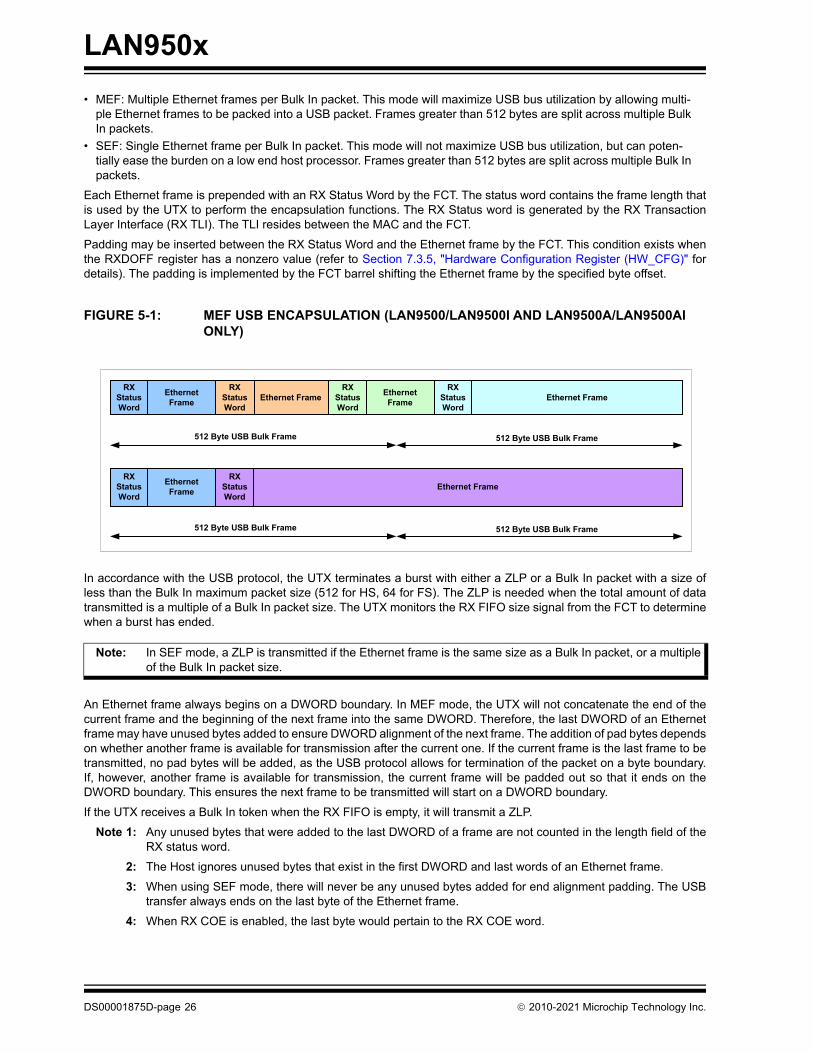
• MEF: Multiple Ethernet frames per Bulk In packet. This mode will maximize USB bus utilization by allowing multi-ple Ethernet frames to be packed into a USB packet. Frames greater than 512 bytes are split across multiple Bulk In packets.
• SEF: Single Ethernet frame per Bulk In packet. This mode will not maximize USB bus utilization, but can poten-tially ease the burden on a low end host processor. Frames greater than 512 bytes are split across multiple Bulk In packets.
Each Ethernet frame is prepended with an RX Status Word by the FCT. The status word contains the frame length thatis used by the UTX to perform the encapsulation functions. The RX Status word is generated by the RX TransactionLayer Interface (RX TLI). The TLI resides between the MAC and the FCT.
Padding may be inserted between the RX Status Word and the Ethernet frame by the FCT. This condition exists whenthe RXDOFF register has a nonzero value (refer to Section 7.3.5, "Hardware Configuration Register (HW_CFG)" fordetails). The padding is implemented by the FCT barrel shifting the Ethernet frame by the specified byte offset.
In accordance with the USB protocol, the UTX terminates a burst with either a ZLP or a Bulk In packet with a size ofless than the Bulk In maximum packet size (512 for HS, 64 for FS). The ZLP is needed when the total amount of datatransmitted is a multiple of a Bulk In packet size. The UTX monitors the RX FIFO size signal from the FCT to determinewhen a burst has ended.
An Ethernet frame always begins on a DWORD boundary. In MEF mode, the UTX will not concatenate the end of thecurrent frame and the beginning of the next frame into the same DWORD. Therefore, the last DWORD of an Ethernetframe may have unused bytes added to ensure DWORD alignment of the next frame. The addition of pad bytes dependson whether another frame is available for transmission after the current one. If the current frame is the last frame to betransmitted, no pad bytes will be added, as the USB protocol allows for termination of the packet on a byte boundary.If, however, another frame is available for transmission, the current frame will be padded out so that it ends on theDWORD boundary. This ensures the next frame to be transmitted will start on a DWORD boundary.
If the UTX receives a Bulk In token when the RX FIFO is empty, it will transmit a ZLP.
Note 1: Any unused bytes that were added to the last DWORD of a frame are not counted in the length field of theRX status word.
2: The Host ignores unused bytes that exist in the first DWORD and last words of an Ethernet frame.
3: When using SEF mode, there will never be any unused bytes added for end alignment padding. The USBtransfer always ends on the last byte of the Ethernet frame.
4: When RX COE is enabled, the last byte would pertain to the RX COE word.
FIGURE 5-1: MEF USB ENCAPSULATION (LAN9500/LAN9500I AND LAN9500A/LAN9500AI ONLY)
Note: In SEF mode, a ZLP is transmitted if the Ethernet frame is the same size as a Bulk In packet, or a multipleof the Bulk In packet size.
RX Status Word
Ethernet Frame
512 Byte USB Bulk Frame
Ethernet FrameRX
Status Word
RX Status Word
Ethernet Frame
RX Status Word
Ethernet Frame
RX Status Word
Ethernet Frame
RX Status Word
Ethernet Frame
512 Byte USB Bulk Frame
512 Byte USB Bulk Frame 512 Byte USB Bulk Frame
DS00001875D-page 26 2010-2021 Microchip Technology Inc.
LAN950x
Once a decision is made to end a transfer and a short packet or ZLP has been sent, it is possible that an Ethernet framewill arrive prior to the UTX seeing an ACK from the Host for the previous Bulk In packet. In this case, the UTX mustcontinue to repeat the short packet or ZLP until the ACK is received for the end of the previous transfer. The UTX mustnot start a new transfer, or re-use the previous data toggle, to begin sending the next Ethernet frame until the ACK hasbeen received for the end of the previous transfer.
In order to more efficiently utilize USB bandwidth in MEF mode, the UTX has a mechanism for delaying the transmissionof a short packet, or ZLP. This mode entails having the UTX wait a time defined by the Bulk In Delay Register(BULK_IN_DLY) before terminating the burst. A value of zero in this register disables this feature. By default, a delay of34 us is used.
After the UTX transmits the last USB wPacketSize packet in a burst, the UTX will enable an internal timer. When theinternal timer is equal to the Bulk In Delay, any Bulk In data will be transmitted upon reception of the next Bulk In Token.If enough data arrives before the timer elapses to build at least one maximum sized packet, then the UTX will transmitthis packet when it receives the next Bulk In Token. After packet transmission, the UTX will then reset its internal timerand delay the short packet, or ZLP, transmission until the Bulk In Delay time elapses.
In the case where the FIFO is empty and a single Ethernet packet less than the USB wPacketSize has been received,the UTX will enable its internal timer. If enough data arrives before the timer elapses to build at least one maximum sizedpacket, then the UTX will transmit this packet when it receives the next Bulk In Token and will reset the internal timer.Otherwise, the short packet, or ZLP, is sent in response to the first Bulk In Token received after the timer expires.
The UTX will NAK any Bulk In tokens while waiting for the Bulk In Delay to elapse. This NAK response is not affectedby the Bulk In Empty Response (BIR). The Bulk In Empty Response (BIR) setting only applies after the Bulk In Delaytime expires.
The UTX, via the Burst Cap Register (BURST_CAP), is capable or prematurely terminating a burst. When the amounttransmitted exceeds the value specified in this register, the UTX transmits a ZLP after the current Bulk In packet com-pletes. The Burst Cap Register (BURST_CAP) uses units of USB packet size (512 bytes). To enable use of the BurstCap register, the Burst Cap Enable (BCE) bit in the Hardware Configuration Register (HW_CFG) must be set. For properoperation, the BURST_CAP field should be set to value greater than 4 for HS mode and greater than 32 for FS mode.Burst Cap enforcement is disabled if BURST_CAP is set to a value less than or equal to 4 for HS mode and less thanor equal to 32 for FS mode.
Whenever Burst Cap enforcement is disabled, the UTX will respond with a ZLP (when Bulk In Empty Response (BIR)=0) or with NAK (when Bulk In Empty Response (BIR) = 1).
Whenever Burst Cap enforcement is enabled (BURST_CAP value is legal), the following holds:
• For HS Operation:- Let BURST = BURST_CAP * 512- The burst may terminate at BURST-4, BURST-3, BURST-2, BURST-1, or BURST bytes, or, when the RX FIFO runs out of
data. The burst is terminated with either a short USB packet or with a ZLP.
• For FS operation:- The burst will terminate after BURST_CAP * 64 bytes.
In the case of an error condition, the UTX will issue a rewind to the FCT. This occurs when the UTX completes trans-mitting a Bulk In packet and does not receive an ACK from the Host. In this case, the next frame received by the UTXwill be another In token and the Bulk In packet is retransmitted. When the ACK is finally received, the UTX notifies theFCT. The FCT will then advance the read head pointer to the next packet.
Note: Ethernet frames are not fragmented across bursts when using Burst Cap Enforcement.
Note: The UTX will never stall the endpoint. The endpoint can only be stalled by the Host.
2010-2021 Microchip Technology Inc. DS00001875D-page 27
LAN950x
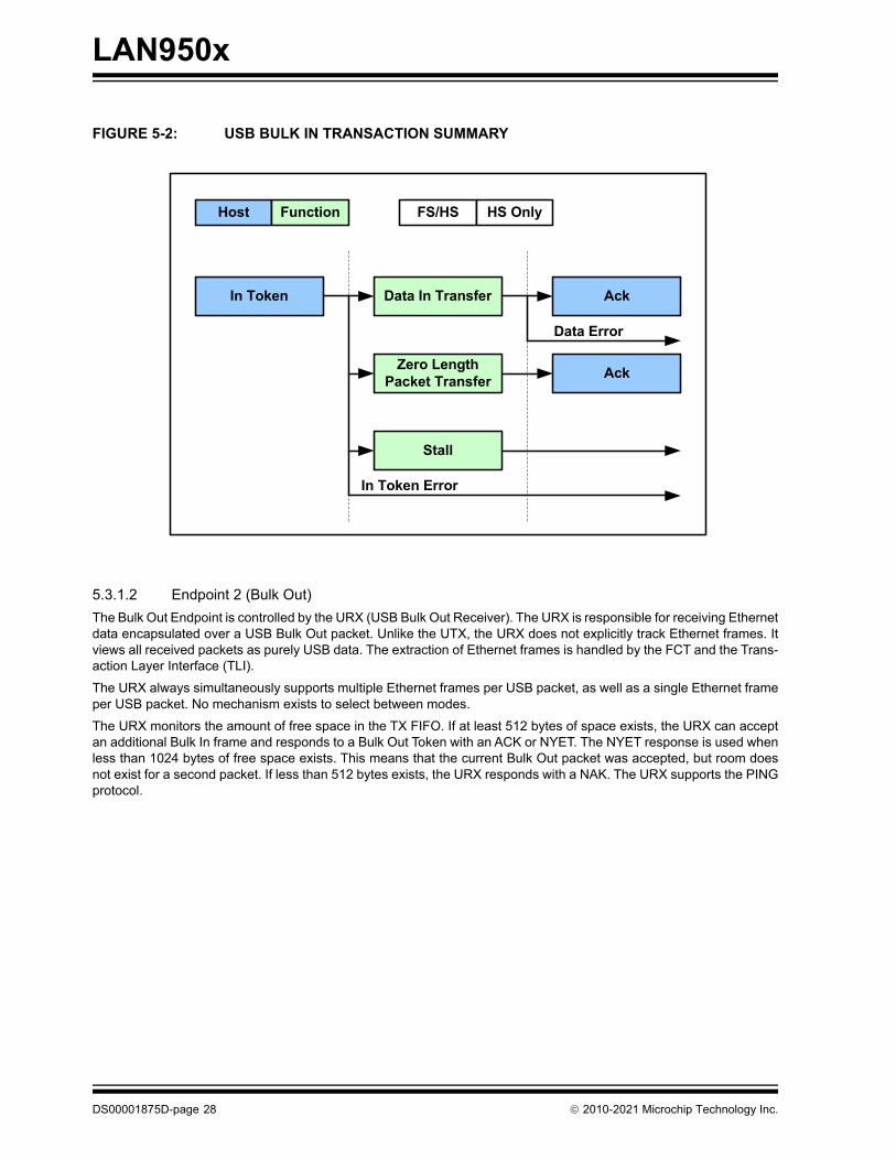
5.3.1.2 Endpoint 2 (Bulk Out)
The Bulk Out Endpoint is controlled by the URX (USB Bulk Out Receiver). The URX is responsible for receiving Ethernetdata encapsulated over a USB Bulk Out packet. Unlike the UTX, the URX does not explicitly track Ethernet frames. Itviews all received packets as purely USB data. The extraction of Ethernet frames is handled by the FCT and the Trans-action Layer Interface (TLI).
The URX always simultaneously supports multiple Ethernet frames per USB packet, as well as a single Ethernet frameper USB packet. No mechanism exists to select between modes.
The URX monitors the amount of free space in the TX FIFO. If at least 512 bytes of space exists, the URX can acceptan additional Bulk In frame and responds to a Bulk Out Token with an ACK or NYET. The NYET response is used whenless than 1024 bytes of free space exists. This means that the current Bulk Out packet was accepted, but room doesnot exist for a second packet. If less than 512 bytes exists, the URX responds with a NAK. The URX supports the PINGprotocol.
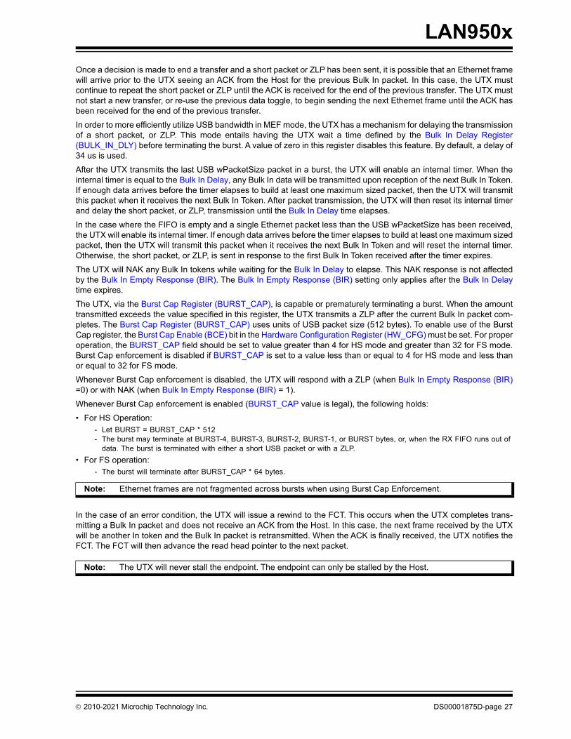
FIGURE 5-2: USB BULK IN TRANSACTION SUMMARY
In Token Data In Transfer Ack
Zero Length Packet Transfer
Stall
Data Error
In Token Error
Host Function FS/HS HS Only
Ack
DS00001875D-page 28 2010-2021 Microchip Technology Inc.
LAN950x
In the case where the Bulk Out packet is errored, the URX does not respond to the Host. The URX will request that theFCT rewinds the packet. It is the Hosts responsibility to retransmit the packet at a later time.
The FCT notifies the URX when it detects loss of sync. When this occurs, the URX stalls the Bulk Out pipe. This is anappropriate response, as loss of sync is a catastrophic error. This behavior is configurable via the Hardware Configura-tion Register (HW_CFG) on page 122.
FIGURE 5-3: USB BULK OUT TRANSACTION SUMMARY
Host Function
Out TokenData Out Transfer
ACK
NYET
STALL
Ping
Data Error
ACK
NAK
NAK
FS/HS HS Only
2010-2021 Microchip Technology Inc. DS00001875D-page 29
LAN950x
5.3.1.3 Endpoint 3 (Interrupt)
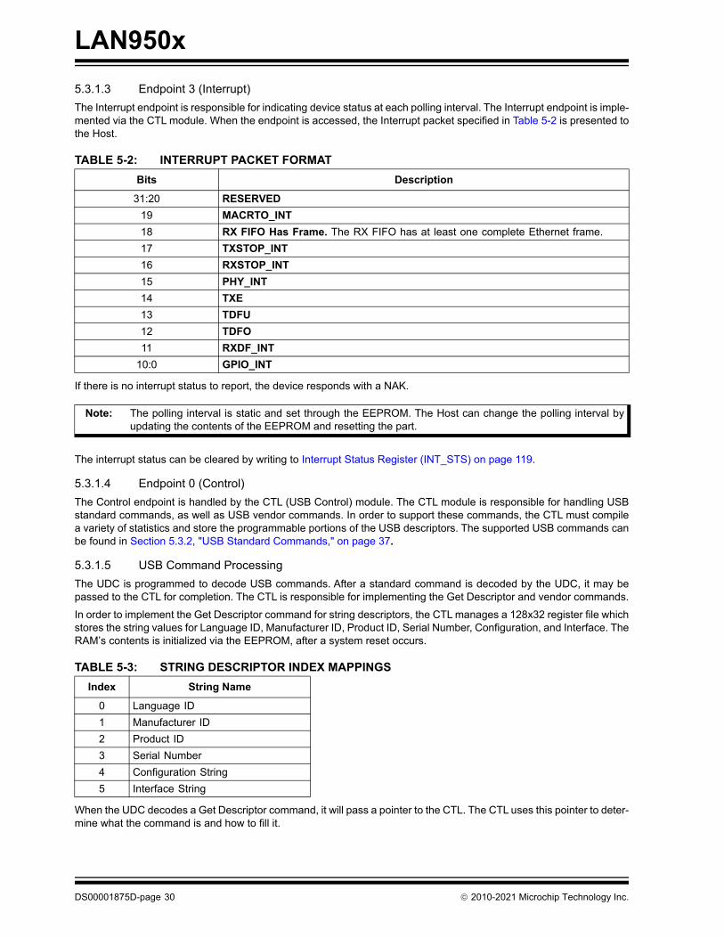
The Interrupt endpoint is responsible for indicating device status at each polling interval. The Interrupt endpoint is imple-mented via the CTL module. When the endpoint is accessed, the Interrupt packet specified in Table 5-2 is presented tothe Host.
If there is no interrupt status to report, the device responds with a NAK.
The interrupt status can be cleared by writing to Interrupt Status Register (INT_STS) on page 119.
5.3.1.4 Endpoint 0 (Control)
The Control endpoint is handled by the CTL (USB Control) module. The CTL module is responsible for handling USBstandard commands, as well as USB vendor commands. In order to support these commands, the CTL must compilea variety of statistics and store the programmable portions of the USB descriptors. The supported USB commands canbe found in Section 5.3.2, "USB Standard Commands," on page 37.
5.3.1.5 USB Command Processing
The UDC is programmed to decode USB commands. After a standard command is decoded by the UDC, it may bepassed to the CTL for completion. The CTL is responsible for implementing the Get Descriptor and vendor commands.
In order to implement the Get Descriptor command for string descriptors, the CTL manages a 128x32 register file whichstores the string values for Language ID, Manufacturer ID, Product ID, Serial Number, Configuration, and Interface. TheRAM’s contents is initialized via the EEPROM, after a system reset occurs.
When the UDC decodes a Get Descriptor command, it will pass a pointer to the CTL. The CTL uses this pointer to deter-mine what the command is and how to fill it.
TABLE 5-2: INTERRUPT PACKET FORMAT
Bits Description
31:20 RESERVED
19 MACRTO_INT
18 RX FIFO Has Frame. The RX FIFO has at least one complete Ethernet frame.
17 TXSTOP_INT
16 RXSTOP_INT
15 PHY_INT
14 TXE
13 TDFU
12 TDFO
11 RXDF_INT
10:0 GPIO_INT
Note: The polling interval is static and set through the EEPROM. The Host can change the polling interval byupdating the contents of the EEPROM and resetting the part.
TABLE 5-3: STRING DESCRIPTOR INDEX MAPPINGS
Index String Name
0 Language ID
1 Manufacturer ID
2 Product ID
3 Serial Number
4 Configuration String
5 Interface String
DS00001875D-page 30 2010-2021 Microchip Technology Inc.
LAN950x
5.3.1.6 USB Descriptors
The following subsections describe the USB descriptors.
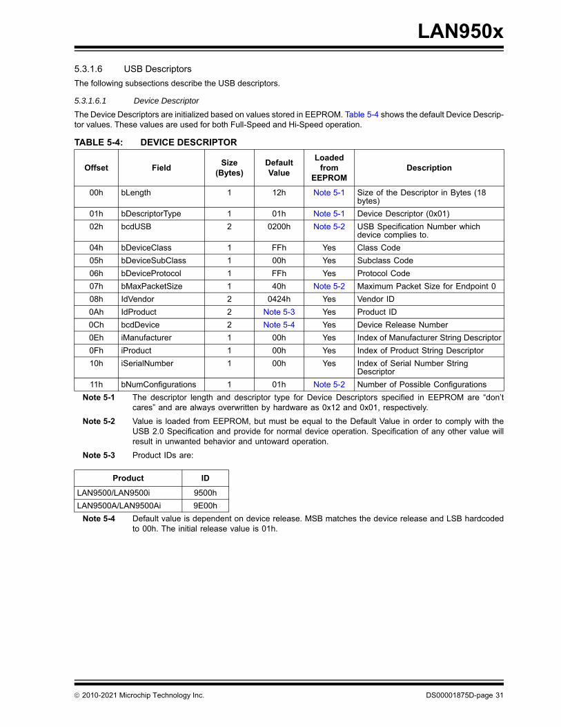
5.3.1.6.1 Device Descriptor
The Device Descriptors are initialized based on values stored in EEPROM. Table 5-4 shows the default Device Descrip-tor values. These values are used for both Full-Speed and Hi-Speed operation.
Note 5-1 The descriptor length and descriptor type for Device Descriptors specified in EEPROM are “don’tcares” and are always overwritten by hardware as 0x12 and 0x01, respectively.
Note 5-2 Value is loaded from EEPROM, but must be equal to the Default Value in order to comply with theUSB 2.0 Specification and provide for normal device operation. Specification of any other value willresult in unwanted behavior and untoward operation.
Note 5-3 Product IDs are:
Note 5-4 Default value is dependent on device release. MSB matches the device release and LSB hardcodedto 00h. The initial release value is 01h.
TABLE 5-4: DEVICE DESCRIPTOR
Offset FieldSize
(Bytes)Default Value
Loaded from
EEPROMDescription
00h bLength 1 12h Note 5-1 Size of the Descriptor in Bytes (18 bytes)
01h bDescriptorType 1 01h Note 5-1 Device Descriptor (0x01)
02h bcdUSB 2 0200h Note 5-2 USB Specification Number which device complies to.
04h bDeviceClass 1 FFh Yes Class Code
05h bDeviceSubClass 1 00h Yes Subclass Code
06h bDeviceProtocol 1 FFh Yes Protocol Code
07h bMaxPacketSize 1 40h Note 5-2 Maximum Packet Size for Endpoint 0
08h IdVendor 2 0424h Yes Vendor ID
0Ah IdProduct 2 Note 5-3 Yes Product ID
0Ch bcdDevice 2 Note 5-4 Yes Device Release Number
0Eh iManufacturer 1 00h Yes Index of Manufacturer String Descriptor
0Fh iProduct 1 00h Yes Index of Product String Descriptor
10h iSerialNumber 1 00h Yes Index of Serial Number String Descriptor
11h bNumConfigurations 1 01h Note 5-2 Number of Possible Configurations
Product ID
LAN9500/LAN9500i 9500h
LAN9500A/LAN9500Ai 9E00h
2010-2021 Microchip Technology Inc. DS00001875D-page 31
LAN950x
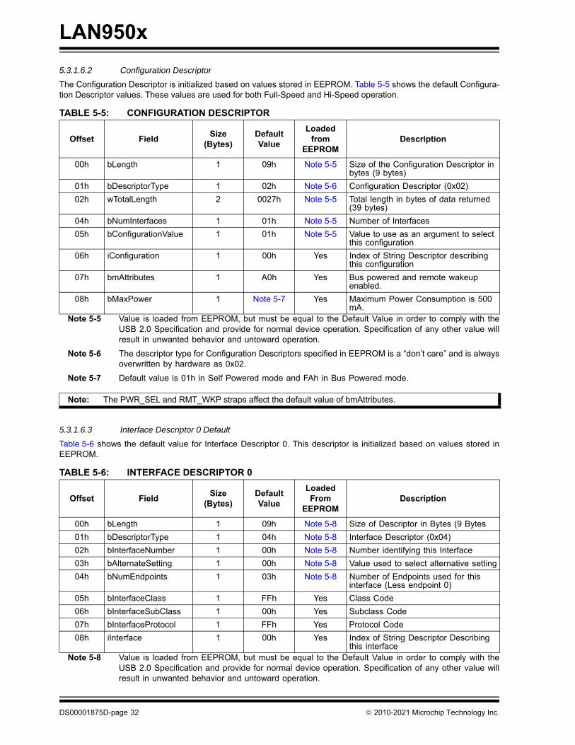
5.3.1.6.2 Configuration Descriptor
The Configuration Descriptor is initialized based on values stored in EEPROM. Table 5-5 shows the default Configura-tion Descriptor values. These values are used for both Full-Speed and Hi-Speed operation.
Note 5-5 Value is loaded from EEPROM, but must be equal to the Default Value in order to comply with theUSB 2.0 Specification and provide for normal device operation. Specification of any other value willresult in unwanted behavior and untoward operation.
Note 5-6 The descriptor type for Configuration Descriptors specified in EEPROM is a “don’t care” and is alwaysoverwritten by hardware as 0x02.
Note 5-7 Default value is 01h in Self Powered mode and FAh in Bus Powered mode.
5.3.1.6.3 Interface Descriptor 0 Default
Table 5-6 shows the default value for Interface Descriptor 0. This descriptor is initialized based on values stored inEEPROM.
Note 5-8 Value is loaded from EEPROM, but must be equal to the Default Value in order to comply with theUSB 2.0 Specification and provide for normal device operation. Specification of any other value willresult in unwanted behavior and untoward operation.
TABLE 5-5: CONFIGURATION DESCRIPTOR
Offset FieldSize
(Bytes)Default Value
Loaded from
EEPROMDescription
00h bLength 1 09h Note 5-5 Size of the Configuration Descriptor in bytes (9 bytes)
01h bDescriptorType 1 02h Note 5-6 Configuration Descriptor (0x02)
02h wTotalLength 2 0027h Note 5-5 Total length in bytes of data returned (39 bytes)
04h bNumInterfaces 1 01h Note 5-5 Number of Interfaces
05h bConfigurationValue 1 01h Note 5-5 Value to use as an argument to select this configuration
06h iConfiguration 1 00h Yes Index of String Descriptor describing this configuration
07h bmAttributes 1 A0h Yes Bus powered and remote wakeup enabled.
08h bMaxPower 1 Note 5-7 Yes Maximum Power Consumption is 500 mA.
Note: The PWR_SEL and RMT_WKP straps affect the default value of bmAttributes.
TABLE 5-6: INTERFACE DESCRIPTOR 0
Offset FieldSize
(Bytes)Default Value
Loaded From
EEPROMDescription
00h bLength 1 09h Note 5-8 Size of Descriptor in Bytes (9 Bytes
01h bDescriptorType 1 04h Note 5-8 Interface Descriptor (0x04)
02h bInterfaceNumber 1 00h Note 5-8 Number identifying this Interface
03h bAlternateSetting 1 00h Note 5-8 Value used to select alternative setting
04h bNumEndpoints 1 03h Note 5-8 Number of Endpoints used for this interface (Less endpoint 0)
05h bInterfaceClass 1 FFh Yes Class Code
06h bInterfaceSubClass 1 00h Yes Subclass Code
07h bInterfaceProtocol 1 FFh Yes Protocol Code
08h iInterface 1 00h Yes Index of String Descriptor Describing this interface
DS00001875D-page 32 2010-2021 Microchip Technology Inc.
LAN950x
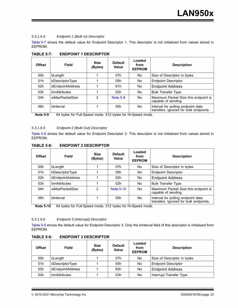
5.3.1.6.4 Endpoint 1 (Bulk In) Descriptor
Table 5-7 shows the default value for Endpoint Descriptor 1. This descriptor is not initialized from values stored inEEPROM.
Note 5-9 64 bytes for Full-Speed mode. 512 bytes for Hi-Speed mode.
5.3.1.6.5 Endpoint 2 (Bulk Out) Descriptor
Table 5-8 shows the default value for Endpoint Descriptor 2. This descriptor is not initialized from values stored inEEPROM.
Note 5-10 64 bytes for Full-Speed mode. 512 bytes for Hi-Speed mode.
5.3.1.6.6 Endpoint 3 (Interrupt) Descriptor
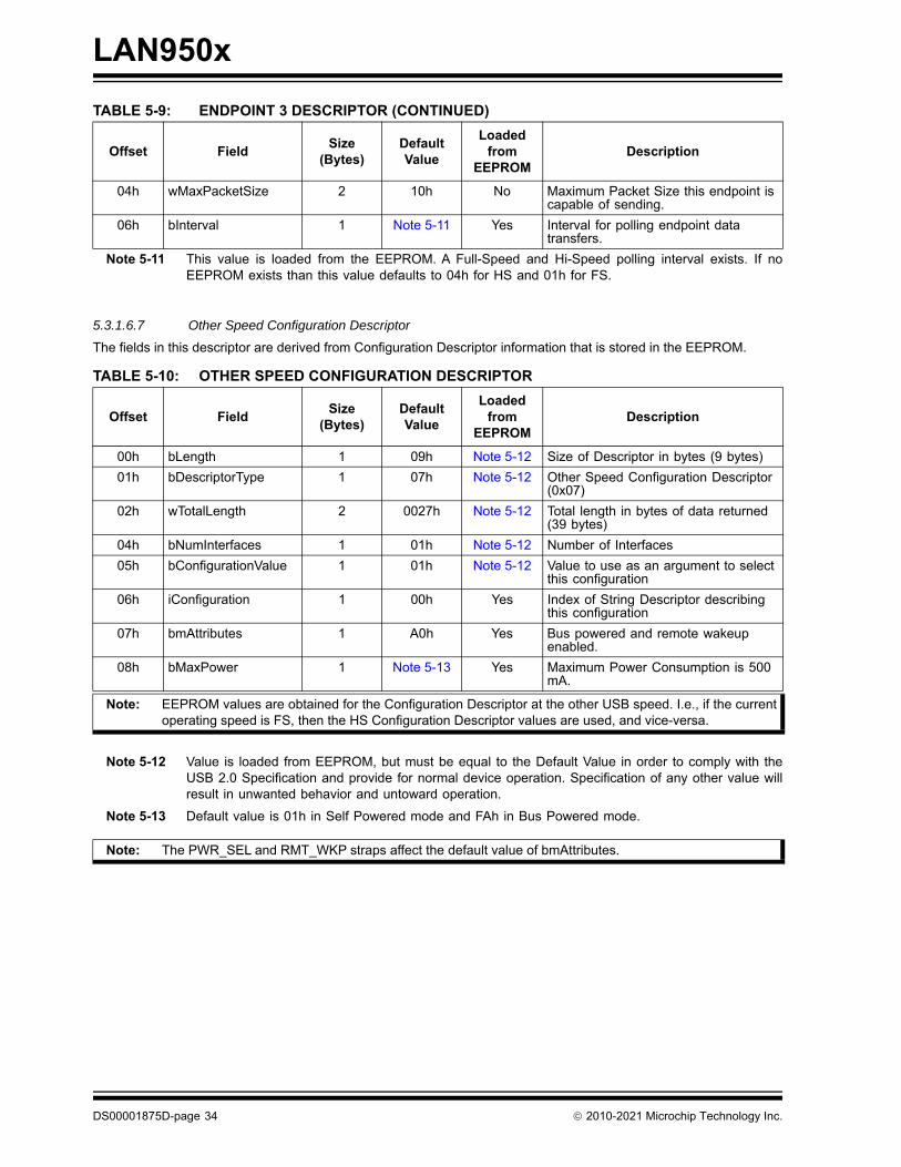
Table 5-9 shows the default value for Endpoint Descriptor 3. Only the bInterval field of this descriptor is initialized fromEEPROM.
TABLE 5-7: ENDPOINT 1 DESCRIPTOR
Offset FieldSize
(Bytes)Default Value
Loaded from
EEPROMDescription
00h bLength 1 07h No Size of Descriptor in bytes
01h bDescriptorType 1 05h No Endpoint Descriptor
02h bEndpointAddress 1 81h No Endpoint Address
03h bmAttributes 1 02h No Bulk Transfer Type
04h wMaxPacketSize 2 Note 5-9 No Maximum Packet Size this endpoint is capable of sending.
06h bInterval 1 00h No Interval for polling endpoint data transfers. Ignored for bulk endpoints.
TABLE 5-8: ENDPOINT 2 DESCRIPTOR
Offset FieldSize
(Bytes)Default Value
Loaded from
EEPROMDescription
00h bLength 1 07h No Size of Descriptor in bytes
01h bDescriptorType 1 05h No Endpoint Descriptor
02h bEndpointAddress 1 02h No Endpoint Address
03h bmAttributes 1 02h No Bulk Transfer Type
04h wMaxPacketSize 2 Note 5-10 No Maximum Packet Size this endpoint is capable of sending.
06h bInterval 1 00h No Interval for polling endpoint data transfers. Ignored for bulk endpoints.
TABLE 5-9: ENDPOINT 3 DESCRIPTOR
Offset FieldSize
(Bytes)Default Value
Loaded from
EEPROMDescription
00h bLength 1 07h No Size of Descriptor in bytes
01h bDescriptorType 1 05h No Endpoint Descriptor
02h bEndpointAddress 1 83h No Endpoint Address
03h bmAttributes 1 03h No Interrupt Transfer Type
2010-2021 Microchip Technology Inc. DS00001875D-page 33
LAN950x
Note 5-11 This value is loaded from the EEPROM. A Full-Speed and Hi-Speed polling interval exists. If noEEPROM exists than this value defaults to 04h for HS and 01h for FS.
5.3.1.6.7 Other Speed Configuration Descriptor
The fields in this descriptor are derived from Configuration Descriptor information that is stored in the EEPROM.
Note 5-12 Value is loaded from EEPROM, but must be equal to the Default Value in order to comply with theUSB 2.0 Specification and provide for normal device operation. Specification of any other value willresult in unwanted behavior and untoward operation.
Note 5-13 Default value is 01h in Self Powered mode and FAh in Bus Powered mode.
04h wMaxPacketSize 2 10h No Maximum Packet Size this endpoint is capable of sending.
06h bInterval 1 Note 5-11 Yes Interval for polling endpoint data transfers.
TABLE 5-10: OTHER SPEED CONFIGURATION DESCRIPTOR
Offset FieldSize
(Bytes)Default Value
Loaded from
EEPROMDescription
00h bLength 1 09h Note 5-12 Size of Descriptor in bytes (9 bytes)
01h bDescriptorType 1 07h Note 5-12 Other Speed Configuration Descriptor (0x07)
02h wTotalLength 2 0027h Note 5-12 Total length in bytes of data returned (39 bytes)
04h bNumInterfaces 1 01h Note 5-12 Number of Interfaces
05h bConfigurationValue 1 01h Note 5-12 Value to use as an argument to select this configuration
06h iConfiguration 1 00h Yes Index of String Descriptor describing this configuration
07h bmAttributes 1 A0h Yes Bus powered and remote wakeup enabled.
08h bMaxPower 1 Note 5-13 Yes Maximum Power Consumption is 500 mA.
Note: EEPROM values are obtained for the Configuration Descriptor at the other USB speed. I.e., if the currentoperating speed is FS, then the HS Configuration Descriptor values are used, and vice-versa.
Note: The PWR_SEL and RMT_WKP straps affect the default value of bmAttributes.
TABLE 5-9: ENDPOINT 3 DESCRIPTOR (CONTINUED)
Offset FieldSize
(Bytes)Default Value
Loaded from
EEPROMDescription
DS00001875D-page 34 2010-2021 Microchip Technology Inc.
LAN950x
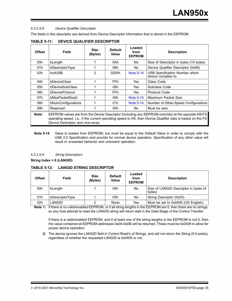
5.3.1.6.8 Device Qualifier Descriptor
The fields in this descriptor are derived from Device Descriptor information that is stored in the EEPROM.
Note 5-14 Value is loaded from EEPROM, but must be equal to the Default Value in order to comply with theUSB 2.0 Specification and provide for normal device operation. Specification of any other value willresult in unwanted behavior and untoward operation.
5.3.1.6.9 String Descriptors
String Index = 0 (LANGID)
Note 1: If there is no valid/enabled EEPROM, or if all string lengths in the EEPROM are 0, then there are no strings,so any host attempt to read the LANGID string will return stall in the Data Stage of the Control Transfer.
If there is a valid/enabled EEPROM, and if at least one of the string lengths in the EEPROM is not 0, thenthe value contained at EEPROM addresses 0x0A-0x0B will be returned. These must be 0x0409 to allow forproper device operation.
2: The device ignores the LANGID field in Control Read’s of Strings, and will not return the String (if it exists),regardless of whether the requested LANGID is 0x0409 or not.
TABLE 5-11: DEVICE QUALIFIER DESCRIPTOR
Offset FieldSize
(Bytes)Default Value
Loaded from
EEPROMDescription
00h bLength 1 0Ah No Size of Descriptor in bytes (10 bytes)
01h bDescriptorType 1 06h No Device Qualifier Descriptor (0x06)
02h bcdUSB 2 0200h Note 5-14 USB Specification Number which device complies to.
04h bDeviceClass 1 FFh Yes Class Code
05h bDeviceSubClass 1 00h Yes Subclass Code
06h bDeviceProtocol 1 FFh Yes Protocol Code
07h bMaxPacketSize0 1 40h Note 5-14 Maximum Packet Size
08h bNumConfigurations 1 01h Note 5-14 Number of Other-Speed Configurations
09h Reserved 1 00h No Must be zero
Note: EEPROM values are from the Device Descriptor (including any EEPROM override) at the opposite HS/FSoperating speed. I.e., if the current operating speed is HS, then Device Qualifier data is based on the FSDevice Descriptor, and vice-versa.
TABLE 5-12: LANGID STRING DESCRIPTOR
Offset FieldSize
(Bytes)Default Value
Loaded from
EEPROMDescription
00h bLength 1 04h No Size of LANGID Descriptor in bytes (4 bytes)
01h bDescriptorType 1 03h No String Descriptor (0x03)
02h LANGID 2 None Yes Must be set to 0x0409 (US English).
2010-2021 Microchip Technology Inc. DS00001875D-page 35
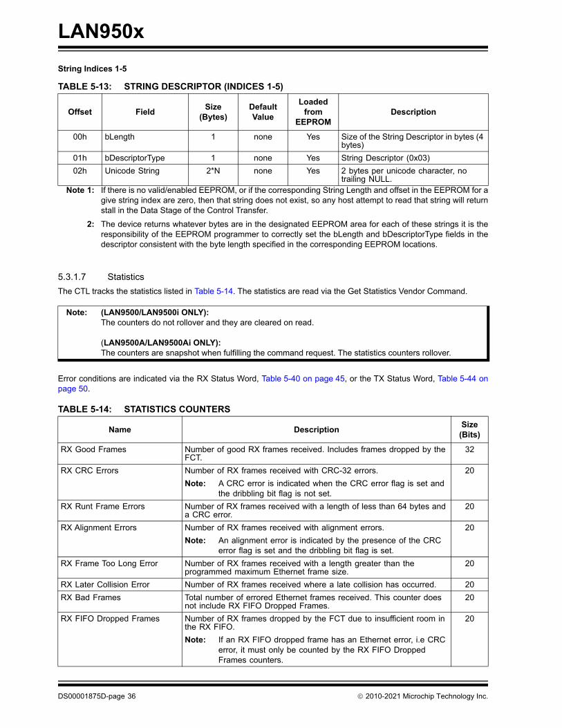
LAN950x
String Indices 1-5
Note 1: If there is no valid/enabled EEPROM, or if the corresponding String Length and offset in the EEPROM for agive string index are zero, then that string does not exist, so any host attempt to read that string will returnstall in the Data Stage of the Control Transfer.
2: The device returns whatever bytes are in the designated EEPROM area for each of these strings it is theresponsibility of the EEPROM programmer to correctly set the bLength and bDescriptorType fields in thedescriptor consistent with the byte length specified in the corresponding EEPROM locations.
5.3.1.7 Statistics
The CTL tracks the statistics listed in Table 5-14. The statistics are read via the Get Statistics Vendor Command.
Error conditions are indicated via the RX Status Word, Table 5-40 on page 45, or the TX Status Word, Table 5-44 onpage 50.
TABLE 5-13: STRING DESCRIPTOR (INDICES 1-5)
Offset FieldSize
(Bytes)Default Value
Loaded from
EEPROMDescription
00h bLength 1 none Yes Size of the String Descriptor in bytes (4 bytes)
01h bDescriptorType 1 none Yes String Descriptor (0x03)
02h Unicode String 2*N none Yes 2 bytes per unicode character, no trailing NULL.
Note: (LAN9500/LAN9500i ONLY):The counters do not rollover and they are cleared on read.
(LAN9500A/LAN9500Ai ONLY):The counters are snapshot when fulfilling the command request. The statistics counters rollover.
TABLE 5-14: STATISTICS COUNTERS
Name DescriptionSize
(Bits)
RX Good Frames Number of good RX frames received. Includes frames dropped by the FCT.
32
RX CRC Errors Number of RX frames received with CRC-32 errors.
Note: A CRC error is indicated when the CRC error flag is set and the dribbling bit flag is not set.
20
RX Runt Frame Errors Number of RX frames received with a length of less than 64 bytes and a CRC error.
20
RX Alignment Errors Number of RX frames received with alignment errors.
Note: An alignment error is indicated by the presence of the CRC error flag is set and the dribbling bit flag is set.
20
RX Frame Too Long Error Number of RX frames received with a length greater than the programmed maximum Ethernet frame size.
20
RX Later Collision Error Number of RX frames received where a late collision has occurred. 20
RX Bad Frames Total number of errored Ethernet frames received. This counter does not include RX FIFO Dropped Frames.
20
RX FIFO Dropped Frames Number of RX frames dropped by the FCT due to insufficient room in the RX FIFO.
Note: If an RX FIFO dropped frame has an Ethernet error, i.e CRC error, it must only be counted by the RX FIFO Dropped Frames counters.
20
DS00001875D-page 36 2010-2021 Microchip Technology Inc.
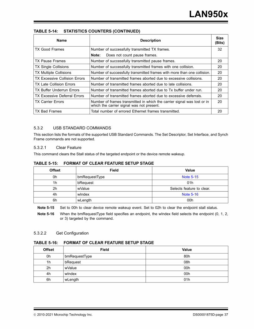
LAN950x
5.3.2 USB STANDARD COMMANDS
This section lists the formats of the supported USB Standard Commands. The Set Descriptor, Set Interface, and SynchFrame commands are not supported.
5.3.2.1 Clear Feature
This command clears the Stall status of the targeted endpoint or the device remote wakeup.
Note 5-15 Set to 00h to clear device remote wakeup event. Set to 02h to clear the endpoint stall status.
Note 5-16 When the bmRequestType field specifies an endpoint, the wIndex field selects the endpoint (0, 1, 2,or 3) targeted by the command.
5.3.2.2 Get Configuration
TX Good Frames Number of successfully transmitted TX frames.
Note: Does not count pause frames.
32
TX Pause Frames Number of successfully transmitted pause frames. 20
TX Single Collisions Number of successfully transmitted frames with one collision. 20
TX Multiple Collisions Number of successfully transmitted frames with more than one collision. 20
TX Excessive Collision Errors Number of transmitted frames aborted due to excessive collisions. 20
TX Late Collision Errors Number of transmitted frames aborted due to late collisions. 20
TX Buffer Underrun Errors Number of transmitted frames aborted due to Tx buffer under run. 20
TX Excessive Deferral Errors Number of transmitted frames aborted due to excessive deferrals. 20
TX Carrier Errors Number of frames transmitted in which the carrier signal was lost or in which the carrier signal was not present.
20
TX Bad Frames Total number of errored Ethernet frames transmitted. 20
TABLE 5-15: FORMAT OF CLEAR FEATURE SETUP STAGE
Offset Field Value
0h bmRequestType Note 5-15
1h bRequest 01h
2h wValue Selects feature to clear.
4h wIndex Note 5-16
6h wLength 00h
TABLE 5-16: FORMAT OF CLEAR FEATURE SETUP STAGE
Offset Field Value
0h bmRequestType 80h
1h bRequest 08h
2h wValue 00h
4h wIndex 00h
6h wLength 01h
TABLE 5-14: STATISTICS COUNTERS (CONTINUED)
Name DescriptionSize
(Bits)
2010-2021 Microchip Technology Inc. DS00001875D-page 37
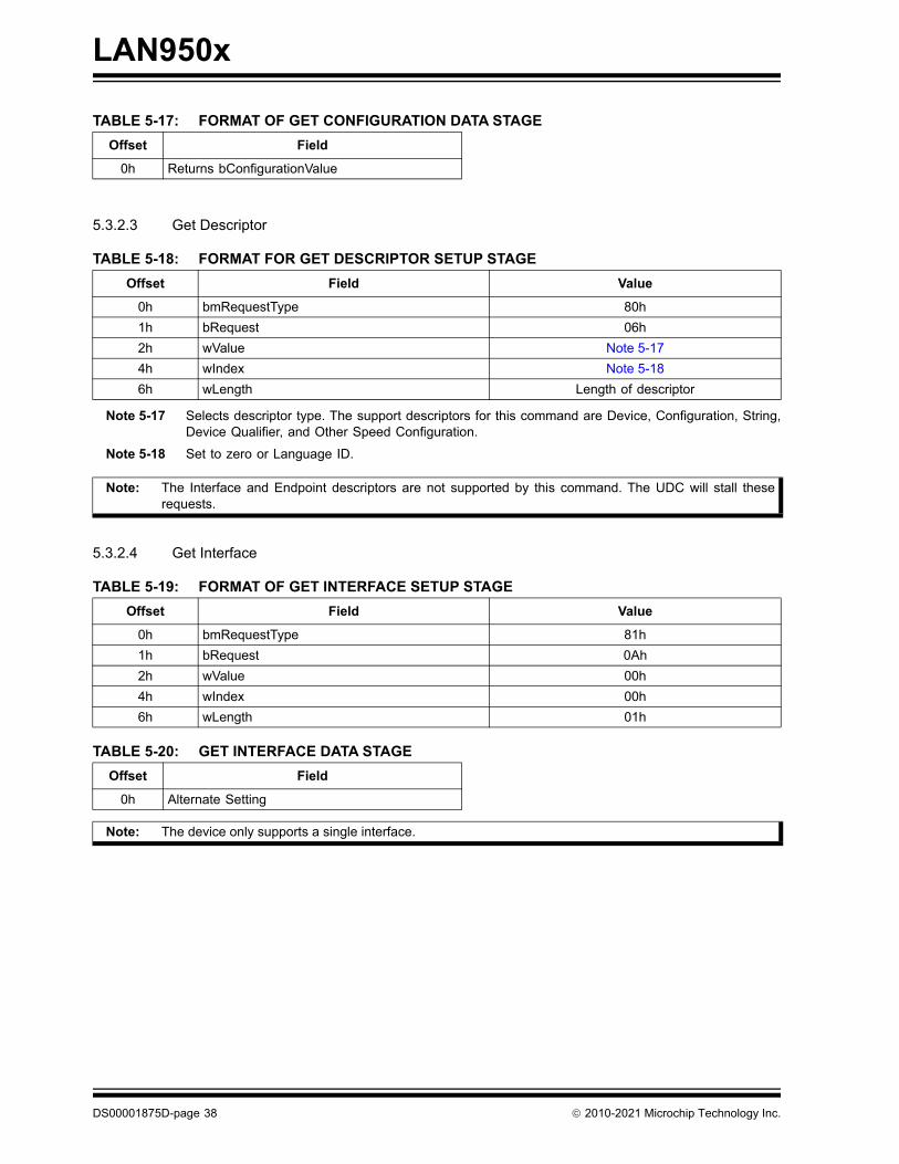
LAN950x
5.3.2.3 Get Descriptor
Note 5-17 Selects descriptor type. The support descriptors for this command are Device, Configuration, String,Device Qualifier, and Other Speed Configuration.
Note 5-18 Set to zero or Language ID.
5.3.2.4 Get Interface
TABLE 5-17: FORMAT OF GET CONFIGURATION DATA STAGE
Offset Field
0h Returns bConfigurationValue
TABLE 5-18: FORMAT FOR GET DESCRIPTOR SETUP STAGE
Offset Field Value
0h bmRequestType 80h
1h bRequest 06h
2h wValue Note 5-17
4h wIndex Note 5-18
6h wLength Length of descriptor
Note: The Interface and Endpoint descriptors are not supported by this command. The UDC will stall theserequests.
TABLE 5-19: FORMAT OF GET INTERFACE SETUP STAGE
Offset Field Value
0h bmRequestType 81h
1h bRequest 0Ah
2h wValue 00h
4h wIndex 00h
6h wLength 01h
TABLE 5-20: GET INTERFACE DATA STAGE
Offset Field
0h Alternate Setting
Note: The device only supports a single interface.
DS00001875D-page 38 2010-2021 Microchip Technology Inc.
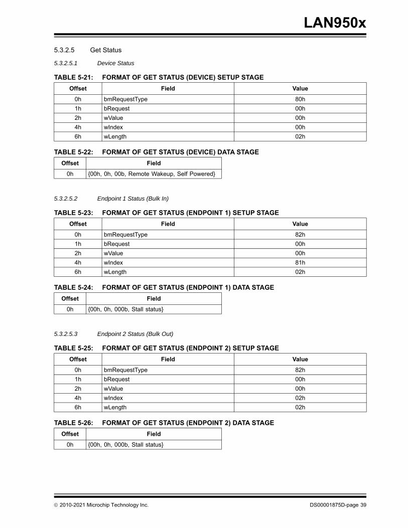
LAN950x
5.3.2.5 Get Status
5.3.2.5.1 Device Status
5.3.2.5.2 Endpoint 1 Status (Bulk In)
5.3.2.5.3 Endpoint 2 Status (Bulk Out)
TABLE 5-21: FORMAT OF GET STATUS (DEVICE) SETUP STAGE
Offset Field Value
0h bmRequestType 80h
1h bRequest 00h
2h wValue 00h
4h wIndex 00h
6h wLength 02h
TABLE 5-22: FORMAT OF GET STATUS (DEVICE) DATA STAGE
Offset Field
0h {00h, 0h, 00b, Remote Wakeup, Self Powered}
TABLE 5-23: FORMAT OF GET STATUS (ENDPOINT 1) SETUP STAGE
Offset Field Value
0h bmRequestType 82h
1h bRequest 00h
2h wValue 00h
4h wIndex 81h
6h wLength 02h
TABLE 5-24: FORMAT OF GET STATUS (ENDPOINT 1) DATA STAGE
Offset Field
0h {00h, 0h, 000b, Stall status}
TABLE 5-25: FORMAT OF GET STATUS (ENDPOINT 2) SETUP STAGE
Offset Field Value
0h bmRequestType 82h
1h bRequest 00h
2h wValue 00h
4h wIndex 02h
6h wLength 02h
TABLE 5-26: FORMAT OF GET STATUS (ENDPOINT 2) DATA STAGE
Offset Field
0h {00h, 0h, 000b, Stall status}
2010-2021 Microchip Technology Inc. DS00001875D-page 39
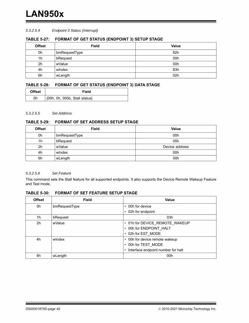
LAN950x
5.3.2.5.4 Endpoint 3 Status (Interrupt)
5.3.2.5.5 Set Address
5.3.2.5.6 Set Feature
This command sets the Stall feature for all supported endpoints. It also supports the Device Remote Wakeup Featureand Test mode.
TABLE 5-27: FORMAT OF GET STATUS (ENDPOINT 3) SETUP STAGE
Offset Field Value
0h bmRequestType 82h
1h bRequest 00h
2h wValue 00h
4h wIndex 83h
6h wLength 02h
TABLE 5-28: FORMAT OF GET STATUS (ENDPOINT 3) DATA STAGE
Offset Field
0h {00h, 0h, 000b, Stall status}
TABLE 5-29: FORMAT OF SET ADDRESS SETUP STAGE
Offset Field Value
0h bmRequestType 00h
1h bRequest 05h
2h wValue Device address
4h wIndex 00h
6h wLength 00h
TABLE 5-30: FORMAT OF SET FEATURE SETUP STAGE
Offset Field Value
0h bmRequestType • 00h for device
• 02h for endpoint
1h bRequest 03h
2h wValue • 01h for DEVICE_REMOTE_WAKEUP
• 00h for ENDPOINT_HALT
• 02h for EST_MODE
4h wIndex • 00h for device remote wakeup
• 00h for TEST_MODE
• Interface endpoint number for halt
6h wLength 00h
DS00001875D-page 40 2010-2021 Microchip Technology Inc.
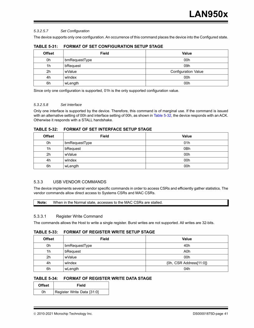
LAN950x
5.3.2.5.7 Set Configuration
The device supports only one configuration. An occurrence of this command places the device into the Configured state.
Since only one configuration is supported, 01h is the only supported configuration value.
5.3.2.5.8 Set Interface
Only one interface is supported by the device. Therefore, this command is of marginal use. If the command is issuedwith an alternative setting of 00h and interface setting of 00h, as shown in Table 5-32, the device responds with an ACK.Otherwise it responds with a STALL handshake.
5.3.3 USB VENDOR COMMANDS
The device implements several vendor specific commands in order to access CSRs and efficiently gather statistics. Thevendor commands allow direct access to Systems CSRs and MAC CSRs.
5.3.3.1 Register Write Command
The commands allows the Host to write a single register. Burst writes are not supported. All writes are 32-bits.
TABLE 5-31: FORMAT OF SET CONFIGURATION SETUP STAGE
Offset Field Value
0h bmRequestType 00h
1h bRequest 09h
2h wValue Configuration Value
4h wIndex 00h
6h wLength 00h
TABLE 5-32: FORMAT OF SET INTERFACE SETUP STAGE
Offset Field Value
0h bmRequestType 01h
1h bRequest 0Bh
2h wValue 00h
4h wIndex 00h
6h wLength 00h
Note: When in the Normal state, accesses to the MAC CSRs are stalled.
TABLE 5-33: FORMAT OF REGISTER WRITE SETUP STAGE
Offset Field Value
0h bmRequestType 40h
1h bRequest A0h
2h wValue 00h
4h wIndex {0h, CSR Address[11:0]}
6h wLength 04h
TABLE 5-34: FORMAT OF REGISTER WRITE DATA STAGE
Offset Field
0h Register Write Data [31:0]
2010-2021 Microchip Technology Inc. DS00001875D-page 41
LAN950x
5.3.3.2 Register Read Command
The commands allows the Host to read a single register. Burst reads are not supported. All reads return 32-bits.
5.3.3.3 Get Statistics Command
The Get Statistics Command returns the entire contents of the statistics RAMs. The wIndex field is used to select theRX or TX statistics.
Note 5-19 0b - Retrieves RX statistics. 1b - Retrieves TX statistics.
Note 5-20 20h for RX statistics. 28h for TX statistics.
TABLE 5-35: FORMAT OF REGISTER READ SETUP STAGE
Offset Field Value
0h bmRequestType C0h
1h bRequest A1h
2h wValue 00h
4h wIndex {0h, CSR Address[11:0]}
6h wLength 04h
TABLE 5-36: FORMAT OF REGISTER READ DATA STAGE
Offset Field
0h Register Read Data [31:0]
Note: (LAN9500/LAN9500i ONLY):The contents of the statistics RAM is cleared after the command is processed.
(LAN9500A/LAN9500Ai ONLY):The contents of the statistics RAM is snapshot when fulfilling the command request. The statistics countersrollover, hence the RAM is not cleared.
TABLE 5-37: FORMAT OF GET STATISTICS SETUP STAGE
Offset Field Value
0h bmRequestType C0h
1h bRequest A2h
2h wValue 00h
4h wIndex Note 5-19
6h wLength Note 5-20
DS00001875D-page 42 2010-2021 Microchip Technology Inc.
LAN950x
5.4 FIFO Controller (FCT)
The FIFO controller uses a 28 KB internal SRAM to buffer RX and TX traffic. 20 KB is allocated for received Ethernet-USB traffic (RX buffer), while 8 KB is allocated for USB-Ethernet traffic (TX buffer).Bulk-Out packets from the USB con-troller are directly stored into the TX buffer. The FCT is responsible for extracting Ethernet frames from the USB packetdata and passing the frames to the MAC.Ethernet Frames are directly stored into the RX buffer and become the basisfor bulk-in packets. The FCT passes the stored data to the UTX in blocks typically 512 or 64 bytes in size, dependingon the current HS/FS USB operating speed.
5.4.1 RX PATH (ETHERNET -> USB)
The 20 KB RX FIFO buffers Ethernet frames received from the TLI. The UTX extracts these frames from the FCT toform USB Bulk In packets. The Host drivers will ultimately reassemble the Ethernet frames from the USB packets.
The FCT manages the writing of data into the RX FIFO through the use of two pointers - the rx_wr_ptr and the rx_wr_h-d_ptr. The rx_wr_ptr is used to write Ethernet frame data into the FIFO. The rx_wr_hd_ptr points to the location prior tothe first DWORD of the frame. It is used to write the RX Status Word received from the TLI, upon completion of a frametransaction. This status word contains status information associated with the frame and the frame transaction. Figure 5-4 illustrates how a frame is stored in the FIFO, along with pointer usage.
When the RX TLI signals that it has Data ready, the RX TLI controller starts passing the RX packet data to the FCT. TheFCT updates the RX FIFO pointers as the data is written into the FIFO. The last transfer from the TLI is the RX StatusWord.
The FCT may insert 0 - 3 bytes at the start of the Ethernet frame. The value of the RX Data Offset (RXDOFF) field ofthe Hardware Configuration Register (HW_CFG) on page 122 determines the number of bytes inserted.
TABLE 5-38: FORMAT OF GET STATISTICS DATA STAGE (RX)
Offset Field
00h RX Good Frames
04h RX CRC Errors
08h RX Runt Frame Errors
0Ch RX Alignment Errors
10h RX Frame Too Long Error
14h RX Later Collision Error
18h RX Bad Frames
1Ch RX FIFO Dropped Frames
TABLE 5-39: FORMAT OF GET STATISTICS DATA STAGE (TX)
Offset Field
00h TX Good Frames
04h TX Pause Frames
08h TX Single Collisions
0Ch TX Multiple Collisions
10h TX Excessive Collision Errors
14h TX Late Collision Errors
18h TX Buffer Underrun Errors
1Ch TX Excessive Deferral Errors
20h TX Carrier Errors
24h TX Bad Frames
2010-2021 Microchip Technology Inc. DS00001875D-page 43
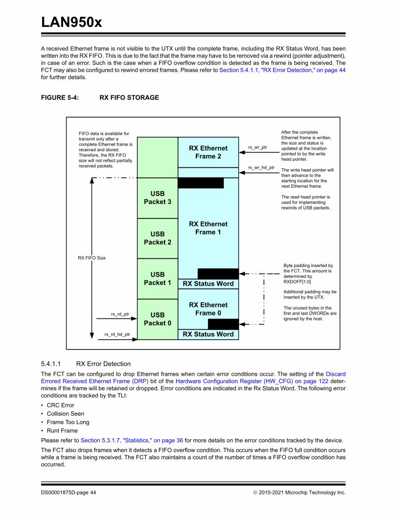
LAN950x
A received Ethernet frame is not visible to the UTX until the complete frame, including the RX Status Word, has beenwritten into the RX FIFO. This is due to the fact that the frame may have to be removed via a rewind (pointer adjustment),in case of an error. Such is the case when a FIFO overflow condition is detected as the frame is being received. TheFCT may also be configured to rewind errored frames. Please refer to Section 5.4.1.1, "RX Error Detection," on page 44for further details.
5.4.1.1 RX Error Detection
The FCT can be configured to drop Ethernet frames when certain error conditions occur. The setting of the DiscardErrored Received Ethernet Frame (DRP) bit of the Hardware Configuration Register (HW_CFG) on page 122 deter-mines if the frame will be retained or dropped. Error conditions are indicated in the Rx Status Word. The following errorconditions are tracked by the TLI:
• CRC Error
• Collision Seen
• Frame Too Long
• Runt Frame
Please refer to Section 5.3.1.7, "Statistics," on page 36 for more details on the error conditions tracked by the device.
The FCT also drops frames when it detects a FIFO overflow condition. This occurs when the FIFO full condition occurswhile a frame is being received. The FCT also maintains a count of the number of times a FIFO overflow condition hasoccurred.
FIGURE 5-4: RX FIFO STORAGE
RX Status Word
RX Ethernet Frame 0
RX Status Word
RX Ethernet Frame 1
rx_rd_ptr
rx_wr_hd_ptr
RX Ethernet Frame 2
rx_wr_ptr
After the complete Ethernet frame is written, the size and status is updated at the location pointed to by the write head pointer.
The write head pointer will then advance to the starting location for the next Ethernet frame.
The read head pointer is used for implementing rewinds of USB packets.
rx_rd_hd_ptr
USBPacket 0
USBPacket 1
USBPacket 2
USBPacket 3
FIFO data is available for transmit only after a complete Ethernet frame is received and stored. Therefore, the RX FIFO size will not reflect partially received packets.
RX FIFO Size
Byte padding inserted by the FCT. This amount is determined by RXDOFF[1:0]
Additional padding may be inserted by the UTX.
The unused bytes in the first and last DWORDs are ignored by the host.
DS00001875D-page 44 2010-2021 Microchip Technology Inc.
LAN950x
Dropping an Ethernet frame is implemented by rewinding the received frame. A write side rewind is implemented bysetting the rx_wr_ptr to be equal to the rx_wr_hd_ptr. Similarly, a read side rewind is implemented by setting therx_rd_ptr to be equal to the rx_rd_hd_ptr.
For the case where the frame is dropped due to overflow, the FCT ignores the remainder of the frame. It will not beginwriting into the RX FIFO again until the next frame is received.
In the read direction, the FCT must also support rewinds for the UTX. This is needed for the case where the USB BulkOut packet is not successfully received by the Host and needs to be retransmitted.
5.4.1.2 RX Status Format
Table 5-40 illustrates the format of the RX Status Word.
TABLE 5-40: RX STATUS WORD FORMAT
Bits Description
31 RESERVED
30 Filtering FailWhen set, this bit indicates that the associated frame failed the address recognizing filtering.
29:16 Frame LengthThe size, in bytes, of the corresponding received frame.
15 Error Status (ES)When set, this bit indicates that the TLI has reported an error. This bit is the logical OR of bits 11, 7, 6, 1 in this status word.
14 RESERVED
13 Broadcast FrameWhen set, this bit indicates that the received frame has a Broadcast address.
12 Length Error (LE)When set, this bit indicates that the actual length does not match with the length/type field of the received frame.
11 Runt FrameWhen set, this bit indicates that frame was prematurely terminated before the collision window (64 bytes). Runt frames are passed on to the Host only if the Pass Bad Frames bit MAC_CR Bit [16] is set.
10 Multicast FrameWhen set, this bit indicates that the received frame has a Multicast address.
9:8 RESERVED
7 Frame Too LongWhen set, this bit indicates that the frame length exceeds the maximum Ethernet specification of 1518 bytes. This is only a frame too long indication and will not cause the frame reception to be truncated.
6 Collision SeenWhen set, this bit indicates that the frame has seen a collision after the collision window. This indicates that a late collision has occurred.
5 Frame TypeWhen set, this bit indicates that the frame is an Ethernet-type frame (Length/Type field in the frame is greater than 1500). When reset, it indicates the incoming frame was an 802.3 type frame. This bit is not set for Runt frames less than 14 bytes.
4 Receive Watchdog time-outWhen set, this bit indicates that the incoming frame is greater than 2048 bytes through 2560 bytes, therefore expiring the Receive Watchdog Timer.
3 MII ErrorWhen set, this bit indicates that a receive error (RX_ER asserted) was detected during frame reception.
2 Dribbling BitWhen set, this bit indicates that the frame contained a no-integer multiple of 8 bits. This error is reported only if the number of dribbling bits in the last byte is 4 in the MII operating mode, or at least 3 in the 10 Mbps operating mode. This bit will not be set when the Collision Seen bit[6] is set. If set and the CRC error[1] bit is reset, then the frame is considered to be valid.
2010-2021 Microchip Technology Inc. DS00001875D-page 45
LAN950x
5.4.1.3 Flushing the RX FIFO
The device allows for the Host to the flush the entire contents of the FCT RX FIFO. When a flush is activated, the readand write pointers of the RX FIFO are returned to their reset state.
Before flushing the RX FIFO, the device’s receiver must be stopped, as specified in Section 5.4.1.4. Once the receiverstop completion is confirmed, the Receive FIFO Flush bit can be set in the Receive Configuration Register (RX_CFG)on page 120 to initiate the flush operation. This bit is cleared after the flush is complete.
5.4.1.4 Stopping and Starting the Receiver
To stop the receiver, the Host must clear the Receiver Enable (RXEN) bit in the MAC Control Register (MAC_CR) onpage 159. When the receiver is halted, the RXSTOP_INT will be pulsed. Once stopped, the Host can optionally clearthe RX Status and RX FIFOs. The Host must re-enable the receiver by setting the RXEN bit.
5.4.2 TX PATH (USB -> ETHERNET)
The 8 KB TX FIFO buffers USB Bulk Out packets received by the URX. The FCT is responsible for extracting the Ether-net frames embedded in the USB Bulk Out Packets and passing them to the TLI. The Ethernet frames were segmentedacross the USB packets by the Host drivers.
The FCT manages the writing of data into the TX FIFO through the use of two pointers - the tx_wr_ptr and the tx_wr_h-d_ptr. These pointers are used to manage the storing of USB Bulk Out packets. They support rewinding the stored USBpacket, in the event that the Bulk Out Packet is errored and needs to be retransmitted by the Host. The write side of theFCT does not perform any processing on the USB packet data. The read side of the TX FIFO is responsible for extract-ing the Ethernet frames. The Ethernet frames may be split across multiple buffers, as shown in Figure 5-5.
1 CRC ErrorWhen set, this bit indicates that a CRC error was detected. This bit is also set when the RX_ER pin is asserted during the reception of a frame even though the CRC may be correct. This bit is not valid if the received frame is a Runt frame, or a late collision was detected or when the Watchdog Time-out occurs.
0 RESERVED
TABLE 5-40: RX STATUS WORD FORMAT (CONTINUED)
Bits Description
DS00001875D-page 46 2010-2021 Microchip Technology Inc.
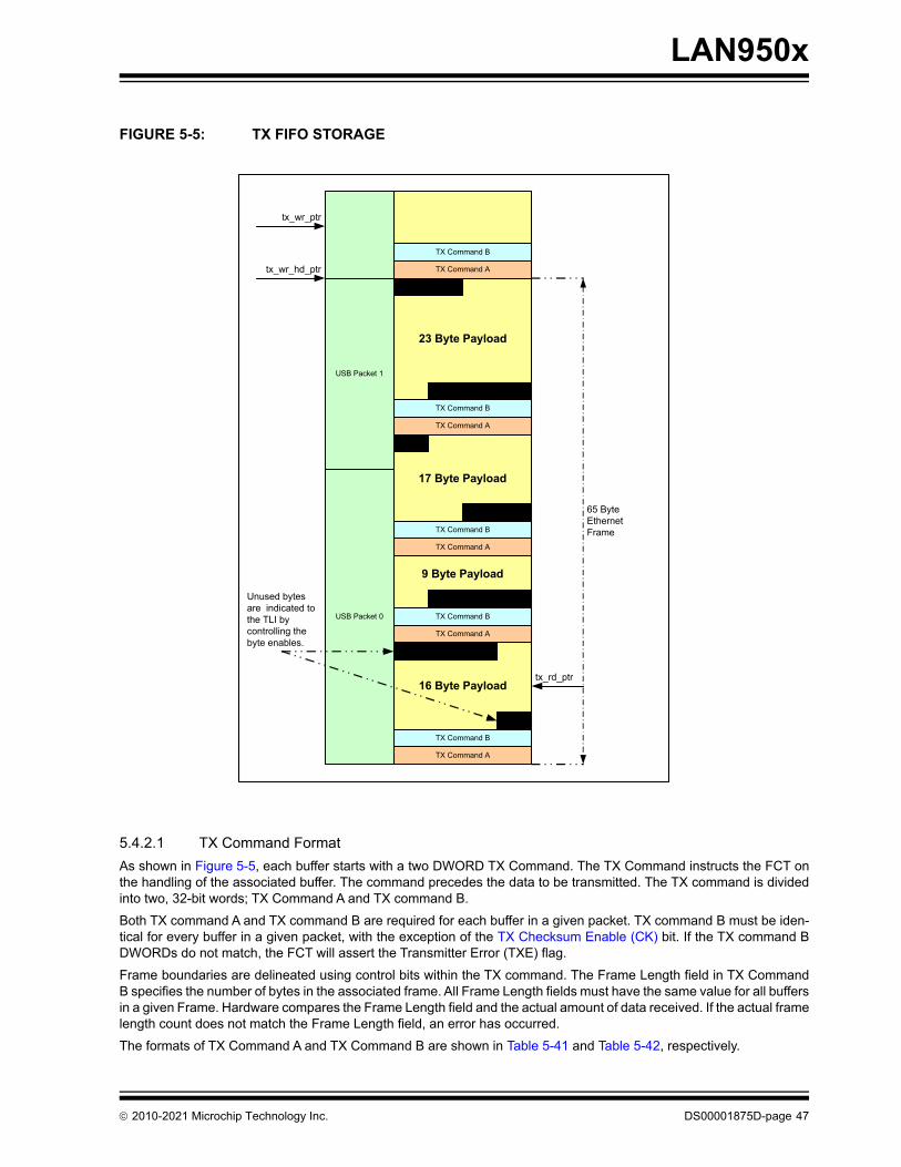
LAN950x
5.4.2.1 TX Command Format
As shown in Figure 5-5, each buffer starts with a two DWORD TX Command. The TX Command instructs the FCT onthe handling of the associated buffer. The command precedes the data to be transmitted. The TX command is dividedinto two, 32-bit words; TX Command A and TX command B.
Both TX command A and TX command B are required for each buffer in a given packet. TX command B must be iden-tical for every buffer in a given packet, with the exception of the TX Checksum Enable (CK) bit. If the TX command BDWORDs do not match, the FCT will assert the Transmitter Error (TXE) flag.
Frame boundaries are delineated using control bits within the TX command. The Frame Length field in TX CommandB specifies the number of bytes in the associated frame. All Frame Length fields must have the same value for all buffersin a given Frame. Hardware compares the Frame Length field and the actual amount of data received. If the actual framelength count does not match the Frame Length field, an error has occurred.
The formats of TX Command A and TX Command B are shown in Table 5-41 and Table 5-42, respectively.
FIGURE 5-5: TX FIFO STORAGE
TX Command A
TX Command B
TX Command A
TX Command B
TX Command A
TX Command B
TX Command A
TX Command B
23 Byte Payload
17 Byte Payload
9 Byte Payload
16 Byte Payload
65 Byte Ethernet Frame
tx_wr_ptr
tx_wr_hd_ptr
USB Packet 0
USB Packet 1
TX Command A
TX Command B
tx_rd_ptr
Unused bytes are indicated to the TLI by controlling the byte enables.
2010-2021 Microchip Technology Inc. DS00001875D-page 47
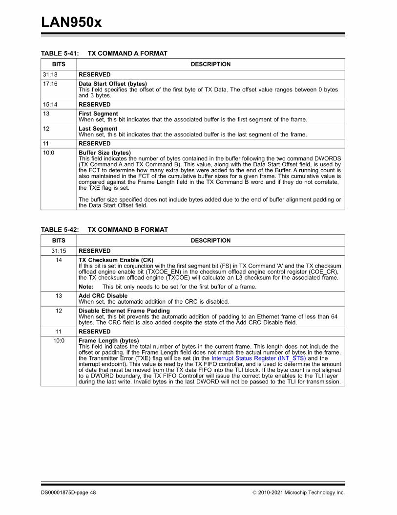
LAN950x
TABLE 5-41: TX COMMAND A FORMAT
BITS DESCRIPTION
31:18 RESERVED
17:16 Data Start Offset (bytes)This field specifies the offset of the first byte of TX Data. The offset value ranges between 0 bytes and 3 bytes.
15:14 RESERVED
13 First SegmentWhen set, this bit indicates that the associated buffer is the first segment of the frame.
12 Last SegmentWhen set, this bit indicates that the associated buffer is the last segment of the frame.
11 RESERVED
10:0 Buffer Size (bytes)This field indicates the number of bytes contained in the buffer following the two command DWORDS (TX Command A and TX Command B). This value, along with the Data Start Offset field, is used by the FCT to determine how many extra bytes were added to the end of the Buffer. A running count is also maintained in the FCT of the cumulative buffer sizes for a given frame. This cumulative value is compared against the Frame Length field in the TX Command B word and if they do not correlate, the TXE flag is set.
The buffer size specified does not include bytes added due to the end of buffer alignment padding or the Data Start Offset field.
TABLE 5-42: TX COMMAND B FORMAT
BITS DESCRIPTION
31:15 RESERVED
14 TX Checksum Enable (CK)If this bit is set in conjunction with the first segment bit (FS) in TX Command 'A' and the TX checksum offload engine enable bit (TXCOE_EN) in the checksum offload engine control register (COE_CR), the TX checksum offload engine (TXCOE) will calculate an L3 checksum for the associated frame.
Note: This bit only needs to be set for the first buffer of a frame.
13 Add CRC DisableWhen set, the automatic addition of the CRC is disabled.
12 Disable Ethernet Frame PaddingWhen set, this bit prevents the automatic addition of padding to an Ethernet frame of less than 64 bytes. The CRC field is also added despite the state of the Add CRC Disable field.
11 RESERVED
10:0 Frame Length (bytes)This field indicates the total number of bytes in the current frame. This length does not include the offset or padding. If the Frame Length field does not match the actual number of bytes in the frame, the Transmitter Error (TXE) flag will be set (in the Interrupt Status Register (INT_STS) and the interrupt endpoint). This value is read by the TX FIFO controller, and is used to determine the amount of data that must be moved from the TX data FIFO into the TLI block. If the byte count is not aligned to a DWORD boundary, the TX FIFO Controller will issue the correct byte enables to the TLI layer during the last write. Invalid bytes in the last DWORD will not be passed to the TLI for transmission.
DS00001875D-page 48 2010-2021 Microchip Technology Inc.
LAN950x
5.4.2.2 TX Data Format
The TX data section begins at the third DWORD in the TX buffer (after TX Command A and TX Command B). The loca-tion of the first byte of valid buffer data to be transmitted is specified in the Data Start Offset field of TX Command A.Table 5-43, "TX Data Start Offset" shows the correlation between the setting of the Lab's in the Data Start Offset fieldand the byte location of the first valid data byte.
TX data is contiguous until the end of the buffer. The buffer may end on a byte boundary. Unused bytes at the end ofthe packet will not be sent to the TLI for transmission.
5.4.2.3 TX Buffer Fragmentation Rules
Transmit buffers must adhere to the following rules:
• Each buffer may start and end on any arbitrary byte alignment.
• The first buffer of any transmit packet can be any length.
• Middle buffers (i.e., those with First Segment = Last Segment = 0) must be greater than, or equal to 4 bytes in length.
• The final buffer of any transmit packet can be any length.
5.4.2.4 FCT Actions
The FCT performs basic sanity checks on the correctness of the buffer configuration, as described in Section 5.4.2.5,"TX Error Detection," on page 49. Errors in this regard indicate the TX path is out of sync, which is catastrophic andrequires a reinitialization of the TX path.
The FCT performs the following steps when extracting an Ethernet frame:
• Strip out TX Command A
• Strip out TX Command B
• Account for the byte offset at the beginning of the frame. Based upon the buffer size and DataStartOffset[1:0] field of TX Command A, the FCT can numerically determine any unused bytes in the first and last word of the buffer. When transferring these respective DWORDs to the TLI, the FCT adjusts the byte enables accordingly.
Unlike the write side, the read side of the TX FIFO does not need to support rewinds. Errors are reported via the Trans-mitter Error (TXE) flag, which is visible to the Host via the Interrupt Endpoint and is also set in theInterrupt Status Reg-ister (INT_STS).
5.4.2.5 TX Error Detection
As previously stated, both TX Command A and TX Command B are required for each buffer in a given frame. TX Com-mand B must be identical for every buffer in a given frame, with the exception of the TX Checksum Enable (CK) bit. Ifthe TX Command B words do not match, then the TX path is out of sync and the FCT asserts the Transmitter Error (TXE)flag.
Similarly, the FCT numerically adds up the size of the frame’s buffers. If there is a numerical mismatch, the TX path isout of sync and the FCT asserts the Transmitter Error (TXE) flag. The following error conditions are tracked by the FCT:
• Missing FS - The expected first buffer of a frame does not have the FS bit set.
• Unexpected FS - The FS bit is set when the total size of buffers so far opened is less than the frame size.
• Missing LS - The total size of the buffers opened is equal to or exceeds the size of the frame. The FCT expects this buffer to have the LS bit set and it is not set.
• Unexpected LS - The LS bit is set when the aggregate total size of descriptor buffers so far opened is less than the frame size.
TABLE 5-43: TX DATA START OFFSET
Data Start Offset[1:0] 11 10 01 00
First TX Data Byte D[31:24] D[23:16] D[15:8] D[7:0]
Note: When a packet is split into multiple buffers, each successive buffer’s data payload may begin on any arbi-trary byte.
2010-2021 Microchip Technology Inc. DS00001875D-page 49
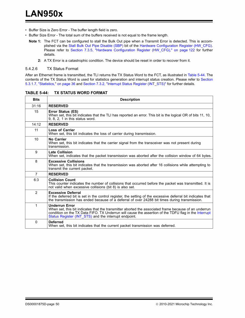
LAN950x
• Buffer Size is Zero Error - The buffer length field is zero.
• Buffer Size Error - The total sum of the buffers received is not equal to the frame length.
Note 1: The FCT can be configured to stall the Bulk Out pipe when a Transmit Error is detected. This is accom-plished via the Stall Bulk Out Pipe Disable (SBP) bit of the Hardware Configuration Register (HW_CFG).Please refer to Section 7.3.5, "Hardware Configuration Register (HW_CFG)," on page 122 for furtherdetails.
2: A TX Error is a catastrophic condition. The device should be reset in order to recover from it.
5.4.2.6 TX Status Format
After an Ethernet frame is transmitted, the TLI returns the TX Status Word to the FCT, as illustrated in Table 5-44. Thecontents of the TX Status Word is used for statistics generation and interrupt status creation. Please refer to Section5.3.1.7, "Statistics," on page 36 and Section 7.3.2, "Interrupt Status Register (INT_STS)" for further details.
TABLE 5-44: TX STATUS WORD FORMAT
Bits Description
31:16 RESERVED
15 Error Status (ES)When set, this bit indicates that the TLI has reported an error. This bit is the logical OR of bits 11, 10, 9, 8, 2, 1 in this status word.
14:12 RESERVED
11 Loss of CarrierWhen set, this bit indicates the loss of carrier during transmission.
10 No CarrierWhen set, this bit indicates that the carrier signal from the transceiver was not present during transmission.
9 Late CollisionWhen set, indicates that the packet transmission was aborted after the collision window of 64 bytes.
8 Excessive CollisionsWhen set, this bit indicates that the transmission was aborted after 16 collisions while attempting to transmit the current packet.
7 RESERVED
6:3 Collision CountThis counter indicates the number of collisions that occurred before the packet was transmitted. It is not valid when excessive collisions (bit 8) is also set.
2 Excessive DeferralIf the deferred bit is set in the control register, the setting of the excessive deferral bit indicates that the transmission has ended because of a deferral of over 24288 bit times during transmission.
1 Underrun ErrorWhen set, this bit indicates that the transmitter aborted the associated frame because of an underrun condition on the TX Data FIFO. TX Underrun will cause the assertion of the TDFU flag in the Interrupt Status Register (INT_STS) and the interrupt endpoint.
0 DeferredWhen set, this bit indicates that the current packet transmission was deferred.
DS00001875D-page 50 2010-2021 Microchip Technology Inc.
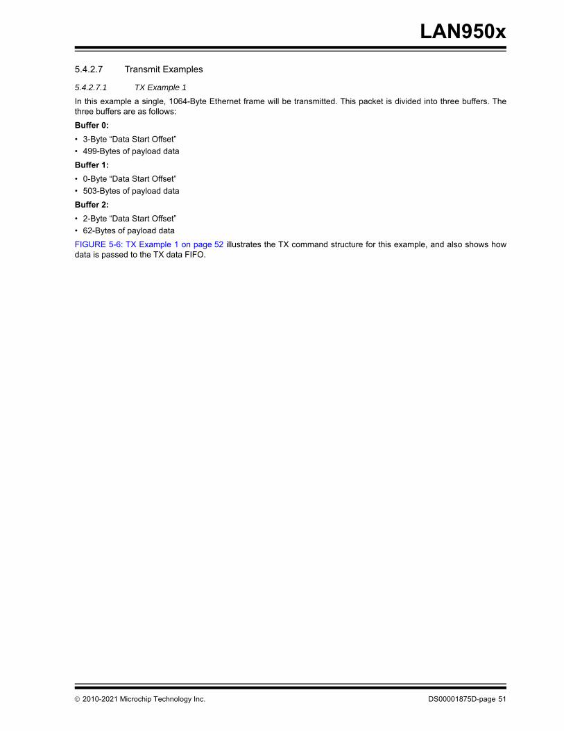
LAN950x
5.4.2.7 Transmit Examples
5.4.2.7.1 TX Example 1
In this example a single, 1064-Byte Ethernet frame will be transmitted. This packet is divided into three buffers. Thethree buffers are as follows:
Buffer 0:
• 3-Byte “Data Start Offset”
• 499-Bytes of payload data
Buffer 1:
• 0-Byte “Data Start Offset”
• 503-Bytes of payload data
Buffer 2:
• 2-Byte “Data Start Offset”
• 62-Bytes of payload data
FIGURE 5-6: TX Example 1 on page 52 illustrates the TX command structure for this example, and also shows howdata is passed to the TX data FIFO.
2010-2021 Microchip Technology Inc. DS00001875D-page 51
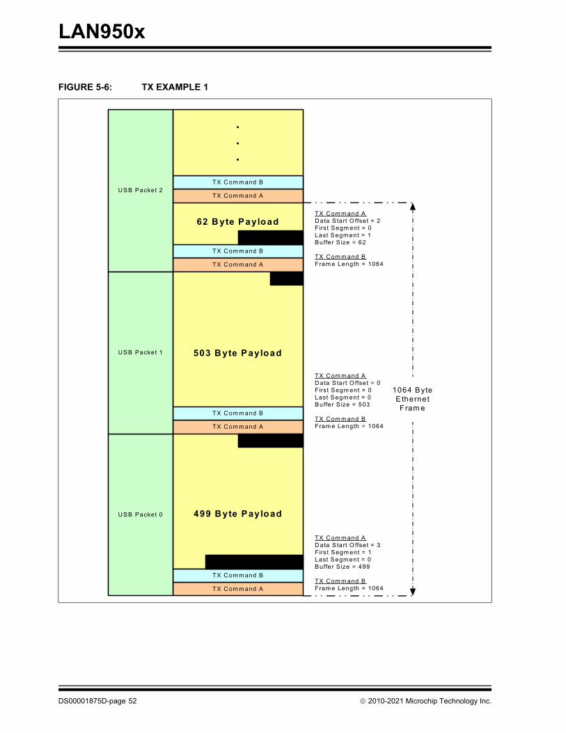
LAN950x
FIGURE 5-6: TX EXAMPLE 1
TX C om m and A
TX C om m and B
TX C om m and A
TX C om m and B
TX C om m and A
TX C om m and B
1064 B yteE thernetFram e
503 B yte Payload
499 B yte PayloadU SB Packet 0
U SB Packet 1
TX C om m and A
TX C om m and B
U SB Packet 2
62 B yte Payload
TX C om m and AD ata S tart O ffset = 3F irst Segm ent = 1Last Segm ent = 0Buffer S ize = 499
TX C om m and BFram e Length = 1064
TX C om m and AD ata S tart O ffset = 0F irst Segm ent = 0Last Segm ent = 0Buffer S ize = 503
TX C om m and BFram e Length = 1064
TX C om m and AD ata S tart O ffset = 2F irst Segm ent = 0Last Segm ent = 1Buffer S ize = 62
TX C om m and BFram e Length = 1064
.
.
.
DS00001875D-page 52 2010-2021 Microchip Technology Inc.
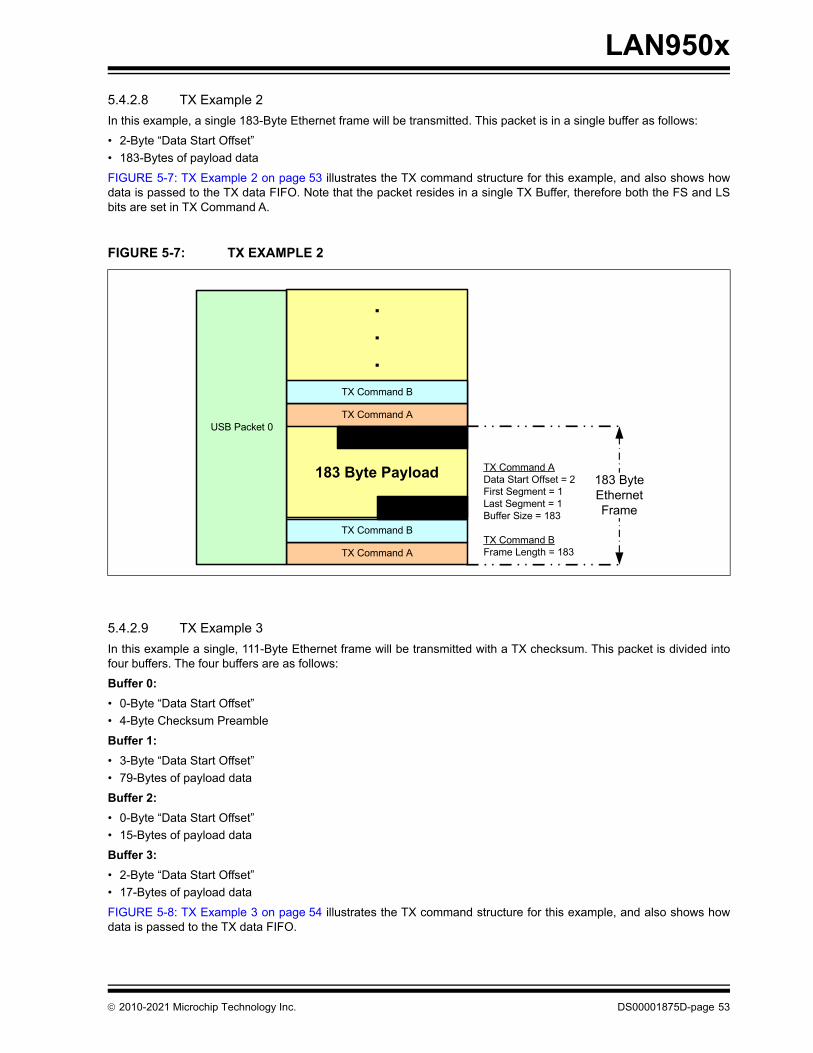
LAN950x
5.4.2.8 TX Example 2
In this example, a single 183-Byte Ethernet frame will be transmitted. This packet is in a single buffer as follows:
• 2-Byte “Data Start Offset”
• 183-Bytes of payload data
FIGURE 5-7: TX Example 2 on page 53 illustrates the TX command structure for this example, and also shows howdata is passed to the TX data FIFO. Note that the packet resides in a single TX Buffer, therefore both the FS and LSbits are set in TX Command A.
5.4.2.9 TX Example 3
In this example a single, 111-Byte Ethernet frame will be transmitted with a TX checksum. This packet is divided intofour buffers. The four buffers are as follows:
Buffer 0:
• 0-Byte “Data Start Offset”
• 4-Byte Checksum Preamble
Buffer 1:
• 3-Byte “Data Start Offset”
• 79-Bytes of payload data
Buffer 2:
• 0-Byte “Data Start Offset”
• 15-Bytes of payload data
Buffer 3:
• 2-Byte “Data Start Offset”
• 17-Bytes of payload data
FIGURE 5-8: TX Example 3 on page 54 illustrates the TX command structure for this example, and also shows howdata is passed to the TX data FIFO.
FIGURE 5-7: TX EXAMPLE 2
TX Command A
TX Command B
TX Command A
TX Command B
183 ByteEthernetFrame
183 Byte Payload
USB Packet 0
TX Command AData Start Offset = 2First Segment = 1Last Segment = 1Buffer Size = 183
TX Command BFrame Length = 183
.
.
.
2010-2021 Microchip Technology Inc. DS00001875D-page 53
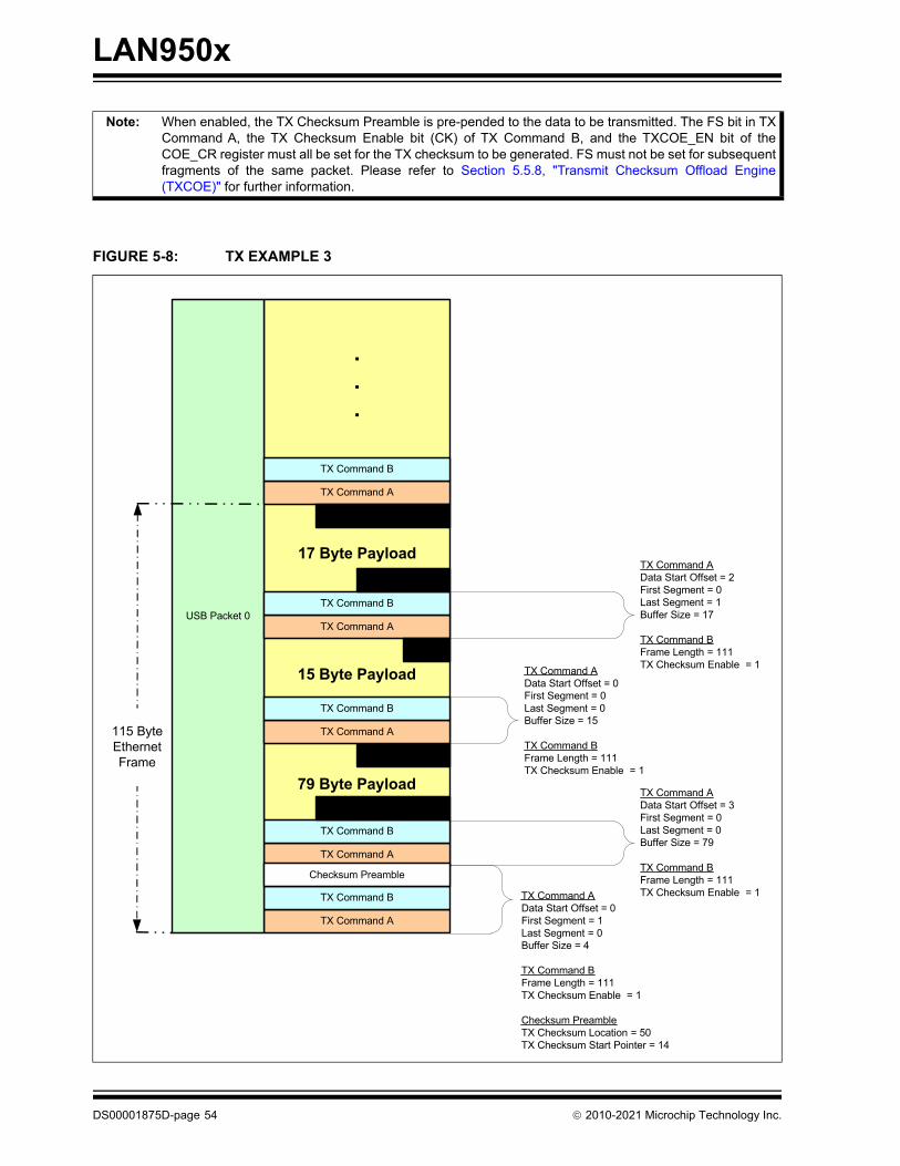
LAN950x
Note: When enabled, the TX Checksum Preamble is pre-pended to the data to be transmitted. The FS bit in TXCommand A, the TX Checksum Enable bit (CK) of TX Command B, and the TXCOE_EN bit of theCOE_CR register must all be set for the TX checksum to be generated. FS must not be set for subsequentfragments of the same packet. Please refer to Section 5.5.8, "Transmit Checksum Offload Engine(TXCOE)" for further information.
FIGURE 5-8: TX EXAMPLE 3
TX Command A
TX Command B
TX Command A
TX Command B
115 ByteEthernetFrame
15 Byte Payload
79 Byte Payload
USB Packet 0
TX Command A
TX Command B
TX Command AData Start Offset = 0First Segment = 1Last Segment = 0Buffer Size = 4
TX Command BFrame Length = 111TX Checksum Enable = 1
Checksum PreambleTX Checksum Location = 50TX Checksum Start Pointer = 14
.
.
.
Checksum Preamble
TX Command AData Start Offset = 3First Segment = 0Last Segment = 0Buffer Size = 79
TX Command BFrame Length = 111TX Checksum Enable = 1
TX Command A
TX Command B
TX Command A
TX Command B
TX Command AData Start Offset = 0First Segment = 0Last Segment = 0Buffer Size = 15
TX Command BFrame Length = 111TX Checksum Enable = 1
TX Command AData Start Offset = 2First Segment = 0Last Segment = 1Buffer Size = 17
TX Command BFrame Length = 111TX Checksum Enable = 1
17 Byte Payload
DS00001875D-page 54 2010-2021 Microchip Technology Inc.
LAN950x
5.4.2.10 Flushing the TX FIFO
The device allows for the Host to the flush the entire contents of the FCT TX FIFO. When a flush is activated, the readand write pointers for the TX FIFO are returned to their reset state.
Before flushing the TX FIFO, the device’s transmitter must be stopped, as specified in Section 5.4.2.11. Once the trans-mitter stop completion is confirmed, the Transmit FIFO Flush bit can be set in the Transmit Configuration Register(TX_CFG) on page 121. This bit is cleared after the flush is complete.
5.4.2.11 Stopping and Starting the Transmitter
To halt the transmitter, the Host must set the Stop Transmitter (STOP_TX) bit in the TX_CFG register. The transmitterwill finish sending the current frame (if there is a frame transmission in progress). When the transmitter has receivedthe TX Status for the current frame, it will clear the STOP_TX and TX_ON bits in the TX_CFG register, and will pulseTXSTOP_INT.
Once stopped, the Host can optionally flush the TX FIFO, and can optionally disable the MAC by clearing TXEN. TheHost must re-enable the transmitter by setting the TX_ON and TXEN bits. If the there are frames pending in the TX FIFO(i.e., the TX FIFO was not purged), the transmission will resume with this data.
5.4.3 ARBITRATION
The FCT must arbitrate access to the RX and TX FIFOs to the URX, UTX, TLI RX, and TLI TX. Highest priority is alwaysgiven to the USB. The TLI RX/TX can be wait stated as frames buffering exists in the TLI (2 KB TX, 128 Byte RX).
FCT strict priority order:
1. URX Request (Bulk Out Packet)
2. UTX Request (Bulk In Packet)
3. TLI RX (Received Ethernet Frame)
4. TLI TX (Transmitted Ethernet Frame)
5.5 10/100 Ethernet MAC
The Ethernet Media Access controller (MAC) incorporates the essential protocol requirements for operating an Ether-net/IEEE 802.3-compliant node and provides an interface between the Host subsystem and the internal Ethernet PHY.The MAC can operate in either 100-Mbps or 10-Mbps mode.
The MAC operates in both half-duplex and full-duplex modes. When operating in half-duplex mode, the MAC compliesfully with Section 4 of ISO/IEC 8802-3 (ANSI/IEEE standard) and ANSI/IEEE 802.3 standards. When operating in full-duplex mode, the MAC complies with IEEE 802.3x full-duplex operation standard.
The MAC provides programmable enhanced features designed to minimize Host supervision, bus utilization, and pre-or post-message processing. These features include the ability to disable retries after a collision, dynamic FCS (FrameCheck Sequence) generation on a frame-by-frame basis, automatic pad field insertion and deletion to enforce minimumframe size attributes, layer 3 checksum calculation for transmit and receive operations, and automatic retransmissionand detection of collision frames.
The MAC can sustain transmission or reception of minimally-sized back-to-back packets at full line speed with an inter-packet gap (IPG) of 9.6 microseconds for 10 Mbps and 0.96 microseconds for 100 Mbps.
The primary attributes of the MAC Function are:
• Transmit and receive message data encapsulation
• Framing (frame boundary delimitation, frame synchronization)
• Error detection (physical medium transmission errors)
• Media access management
Note: The TX Stop mechanism described here assumes that the MAC will return a status for every TX frame.
Note: By nature of the USB bus and UDC operation, the URX and UTX should not request bandwidth simultane-ously.
2010-2021 Microchip Technology Inc. DS00001875D-page 55
LAN950x
• Medium allocation (collision detection, except in full-duplex operation)
• Contention resolution (collision handling, except in full-duplex operation)
• Flow control during full-duplex mode
• Decoding of control frames (PAUSE command) and disabling the transmitter
• Generation of control frames
• Interface to the internal PHY and optional external PHY.
• Checksum offload engine for calculation of layer 3 transmit and receive checksum.
The transmit and receive data paths are separate within the device from the MAC to Host interface, allowing the highestperformance, especially in full duplex mode. Payload data as well as transmit and receive status are passed on thesebusses.
A third internal bus is used to access the MAC’s “Control and Status Registers” (CSR’s). This bus is also accessiblefrom the Host.
On the backend, the MAC interfaces with the 10/100 PHY through an MII (Media Independent Interface) port which isinternal to the device. In addition, there is an external MII interface supporting optional PHY devices. The MAC CSR'salso provide a mechanism for accessing the PHY’s internal registers through the internal SMI (Serial Management Inter-face) bus.
The receive and transmit FIFOs allow increased packet buffer storage to the MAC. The FIFOs are a conduit betweenthe Host interface and the MAC through which all transmitted and received data and status information is passed. DeepFIFOs allow a high degree of latency tolerance relative to the various transport and OS software stacks reducing andminimizing overrun conditions. Like the MAC, the FIFOs have separate receive and transmit data paths.
5.5.1 FLOW CONTROL
The device’s Ethernet MAC supports full-duplex flow control using the pause operation and control frame. It also sup-ports half-duplex flow control using back pressure. In order for flow control to be invoked, the Flow Control Enable(FCEN) bit of the Flow Control Register (FLOW) must be set.
5.5.1.1 Full-Duplex Flow Control
The pause operation inhibits data transmission of data frames for a specified period of time. A Pause operation consistsof a frame containing the globally assigned multicast address (01-80-C2-00-00-01), the PAUSE opcode, and a param-eter indicating the quantum of slot time (512 bit times) to inhibit data transmissions. The PAUSE parameter may rangefrom 0 to 65,535 slot times. The Ethernet MAC logic, on receiving a frame with the reserved multicast address andPAUSE opcode, inhibits data frame transmissions for the length of time indicated. If a Pause request is received whilea transmission is in progress, then the pause will take effect after the transmission is complete. Control frames arereceived and processed by the MAC and are passed on.
The device will automatically transmit pause frames based on the settings of Automatic Flow Control Configuration Reg-ister (AFC_CFG) and the Flow Control Register (FLOW). When the RX FIFO reaches the level set in the Automatic FlowControl High Level (AFC_HI) field of AFC_CFG, the device will transmit a pause frame. The pause time field that is trans-mitted is set in the Pause Time (FCPT) field of the FLOW register. When the RX FIFO drops below the level set in theAutomatic Flow Control Low Level (AFC_LO) field of AFC_CFG, the device will automatically transmit a pause framewith a pause time of zero. The device will only send another pause frame when the RX FIFO level falls below AFC_LOand then exceeds AFC_HI again.
5.5.1.2 Half-Duplex Flow Control (Backpressure)
In half-duplex mode, back pressure is used for flow control. Whenever the RX FIFO crosses a certain threshold level,the MAC starts sending a Jam signal. The MAC transmit logic enters a state at the end of current transmission (if any),where it waits for the beginning of a received frame. Once a new frame starts, the MAC starts sending the jam signal,which will result in a collision. After sensing the collision, the remote station will back off its transmission. The MAC con-tinues sending the jam signal to make other stations defer transmission. The MAC only generates this collision-basedback pressure when it receives a new frame, in order to avoid any late collisions.
The device will automatically assert back pressure based on the setting of the Automatic Flow Control ConfigurationRegister (AFC_CFG). When the RX FIFO reaches the level set by Automatic Flow Control High Level (AFC_HI) field ofAFC_CFG, the Back pressure Duration Timer will start. The device will assert back pressure for any received frames,as defined by the values of the FCANY, FCADD, FCMULT and FCBRD control bits of AFC_CFG. This continues untilthe Back pressure Duration Timer reaches the time specified by the BACK_DUR field of AFC_CFG. After theBACK_DUR time period has elapsed, the receiver will accept one frame. If, after receiving one RX frame, the RX FIFO
DS00001875D-page 56 2010-2021 Microchip Technology Inc.
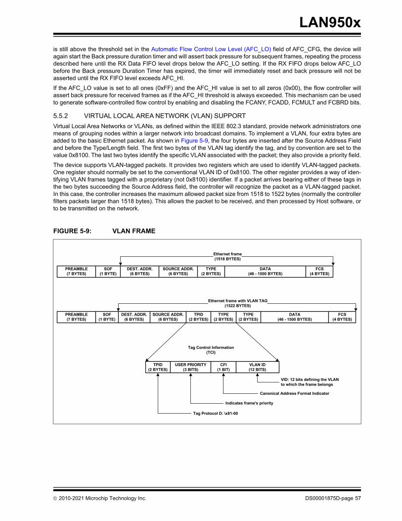
LAN950x
is still above the threshold set in the Automatic Flow Control Low Level (AFC_LO) field of AFC_CFG, the device willagain start the Back pressure duration timer and will assert back pressure for subsequent frames, repeating the processdescribed here until the RX Data FIFO level drops below the AFC_LO setting. If the RX FIFO drops below AFC_LObefore the Back pressure Duration Timer has expired, the timer will immediately reset and back pressure will not beasserted until the RX FIFO level exceeds AFC_HI.
If the AFC_LO value is set to all ones (0xFF) and the AFC_HI value is set to all zeros (0x00), the flow controller willassert back pressure for received frames as if the AFC_HI threshold is always exceeded. This mechanism can be usedto generate software-controlled flow control by enabling and disabling the FCANY, FCADD, FCMULT and FCBRD bits.
5.5.2 VIRTUAL LOCAL AREA NETWORK (VLAN) SUPPORT
Virtual Local Area Networks or VLANs, as defined within the IEEE 802.3 standard, provide network administrators onemeans of grouping nodes within a larger network into broadcast domains. To implement a VLAN, four extra bytes areadded to the basic Ethernet packet. As shown in Figure 5-9, the four bytes are inserted after the Source Address Fieldand before the Type/Length field. The first two bytes of the VLAN tag identify the tag, and by convention are set to thevalue 0x8100. The last two bytes identify the specific VLAN associated with the packet; they also provide a priority field.
The device supports VLAN-tagged packets. It provides two registers which are used to identify VLAN-tagged packets.One register should normally be set to the conventional VLAN ID of 0x8100. The other register provides a way of iden-tifying VLAN frames tagged with a proprietary (not 0x8100) identifier. If a packet arrives bearing either of these tags inthe two bytes succeeding the Source Address field, the controller will recognize the packet as a VLAN-tagged packet.In this case, the controller increases the maximum allowed packet size from 1518 to 1522 bytes (normally the controllerfilters packets larger than 1518 bytes). This allows the packet to be received, and then processed by Host software, orto be transmitted on the network.
FIGURE 5-9: VLAN FRAME
PREAMBLE(7 BYTES)
SOF(1 BYTE)
DEST. ADDR.(6 BYTES)
SOURCE ADDR.(6 BYTES)
TYPE(2 BYTES)
DATA(46 - 1500 BYTES)
FCS(4 BYTES)
Ethernet frame(1518 BYTES)
PREAMBLE(7 BYTES)
SOF(1 BYTE)
DEST. ADDR.(6 BYTES)
SOURCE ADDR.(6 BYTES)
TYPE(2 BYTES)
DATA(46 - 1500 BYTES)
FCS(4 BYTES)
Ethernet frame with VLAN TAG(1522 BYTES)
TPID(2 BYTES)
TYPE(2 BYTES)
TPID(2 BYTES)
USER PRIORITY(3 BITS)
CFI (1 BIT)
VLAN ID (12 BITS)
Tag Control Information(TCI)
Tag Protocol D: \x81-00
Indicates frame's priority
Canonical Address Format Indicator
VID: 12 bits defining the VLAN to which the frame belongs
2010-2021 Microchip Technology Inc. DS00001875D-page 57
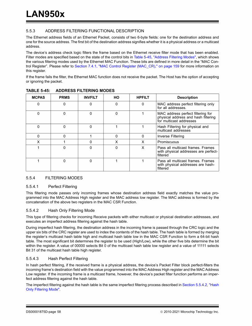
LAN950x
5.5.3 ADDRESS FILTERING FUNCTIONAL DESCRIPTION
The Ethernet address fields of an Ethernet Packet, consists of two 6-byte fields: one for the destination address andone for the source address. The first bit of the destination address signifies whether it is a physical address or a multicastaddress.
The device’s address check logic filters the frame based on the Ethernet receive filter mode that has been enabled.Filter modes are specified based on the state of the control bits in Table 5-45, "Address Filtering Modes", which showsthe various filtering modes used by the Ethernet MAC Function. These bits are defined in more detail in the “MAC Con-trol Register”. Please refer to Section 7.4.1, "MAC Control Register (MAC_CR)," on page 159 for more information onthis register.
If the frame fails the filter, the Ethernet MAC function does not receive the packet. The Host has the option of acceptingor ignoring the packet.
5.5.4 FILTERING MODES
5.5.4.1 Perfect Filtering
This filtering mode passes only incoming frames whose destination address field exactly matches the value pro-grammed into the MAC Address High register and the MAC address low register. The MAC address is formed by theconcatenation of the above two registers in the MAC CSR Function.
5.5.4.2 Hash Only Filtering Mode
This type of filtering checks for incoming Receive packets with either multicast or physical destination addresses, andexecutes an imperfect address filtering against the hash table.
During imperfect hash filtering, the destination address in the incoming frame is passed through the CRC logic and theupper six bits of the CRC register are used to index the contents of the hash table. The hash table is formed by mergingthe register’s multicast hash table high and multicast hash table low in the MAC CSR Function to form a 64-bit hashtable. The most significant bit determines the register to be used (High/Low), while the other five bits determine the bitwithin the register. A value of 00000 selects Bit 0 of the multicast hash table low register and a value of 11111 selectsBit 31 of the multicast hash table high register.
5.5.4.3 Hash Perfect Filtering
In hash perfect filtering, if the received frame is a physical address, the device’s Packet Filter block perfect-filters theincoming frame’s destination field with the value programmed into the MAC Address High register and the MAC AddressLow register. If the incoming frame is a multicast frame, however, the device’s packet filter function performs an imper-fect address filtering against the hash table.
The imperfect filtering against the hash table is the same imperfect filtering process described in Section 5.5.4.2, "HashOnly Filtering Mode".
TABLE 5-45: ADDRESS FILTERING MODES
MCPAS PRMS INVFILT HO HPFILT Description
0 0 0 0 0 MAC address perfect filtering only for all addresses.
0 0 0 0 1 MAC address perfect filtering for physical address and hash filtering for multicast addresses
0 0 0 1 1 Hash Filtering for physical and multicast addresses
0 0 1 0 0 Inverse Filtering
X 1 0 X X Promiscuous
1 0 0 0 X Pass all multicast frames. Frames with physical addresses are perfect-filtered
1 0 0 1 1 Pass all multicast frames. Frames with physical addresses are hash-filtered
DS00001875D-page 58 2010-2021 Microchip Technology Inc.
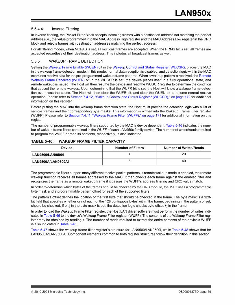
LAN950x
5.5.4.4 Inverse Filtering
In inverse filtering, the Packet Filter Block accepts incoming frames with a destination address not matching the perfectaddress (i.e., the value programmed into the MAC Address High register and the MAC Address Low register in the CRCblock and rejects frames with destination addresses matching the perfect address.
For all filtering modes, when MCPAS is set, all multicast frames are accepted. When the PRMS bit is set, all frames areaccepted regardless of their destination address. This includes all broadcast frames as well.
5.5.5 WAKEUP FRAME DETECTION
Setting the Wakeup Frame Enable (WUEN) bit in the Wakeup Control and Status Register (WUCSR), places the MACin the wakeup frame detection mode. In this mode, normal data reception is disabled, and detection logic within the MACexamines receive data for the pre-programmed wakeup frame patterns. When a wakeup pattern is received, the RemoteWakeup Frame Received (WUFR) bit in the WUCSR is set, the device places itself in a fully operational state, andremote wakeup is issued. The Host will then resume the device and read the WUSCR register to determine the conditionthat caused the remote wakeup. Upon determining that the WUFR bit is set, the Host will know a wakeup frame detec-tion event was the cause. The Host will then clear the WUFR bit, and clear the WUEN bit to resume normal receiveoperation. Please refer to Section 7.4.12, "Wakeup Control and Status Register (WUCSR)," on page 172 for additionalinformation on this register.
Before putting the MAC into the wakeup frame detection state, the Host must provide the detection logic with a list ofsample frames and their corresponding byte masks. This information is written into the Wakeup Frame Filter register(WUFF). Please refer to Section 7.4.11, "Wakeup Frame Filter (WUFF)," on page 171 for additional information on thisregister.
The number of programmable wakeup filters supported by the MAC is device dependent. Table 5-46 indicates the num-ber of wakeup frame filters contained in the WUFF of each LAN950x family device. The number of writes/reads requiredto program the WUFF or read its contents, respectively, is also indicated.
The programmable filters support many different receive packet patterns. If remote wakeup mode is enabled, the remotewakeup function receives all frames addressed to the MAC. It then checks each frame against the enabled filter andrecognizes the frame as a remote wakeup frame if it passes the WUFF’s address filtering and CRC value match.
In order to determine which bytes of the frames should be checked by the CRC module, the MAC uses a programmablebyte mask and a programmable pattern offset for each of the supported filters.
The pattern’s offset defines the location of the first byte that should be checked in the frame. The byte mask is a 128-bit field that specifies whether or not each of the 128 contiguous bytes within the frame, beginning in the pattern offset,should be checked. If bit j in the byte mask is set, the detection logic checks byte offset +j in the frame.
In order to load the Wakeup Frame Filter register, the Host LAN driver software must perform the number of writes indi-cated in Table 5-46 to the device’s Wakeup Frame Filter register (WUFF). The contents of the Wakeup Frame Filter reg-ister may be obtained by reading it. The number of reads required to extract the entire contents of the device’s WUFFis also indicated in Table 5-46.
Table 5-47 shows the wakeup frame filter register’s structure for LAN9500/LAN9500i, while Table 5-48 shows that forLAN9500A/LAN9500Ai. Component elements common to both register structures follow their definition in this section.
TABLE 5-46: WAKEUP FRAME FILTER CAPACITY
Device Number of Filters Number of Writes/Reads
LAN9500/LAN9500i 4 20
LAN9500A/LAN9500Ai 8 40
2010-2021 Microchip Technology Inc. DS00001875D-page 59
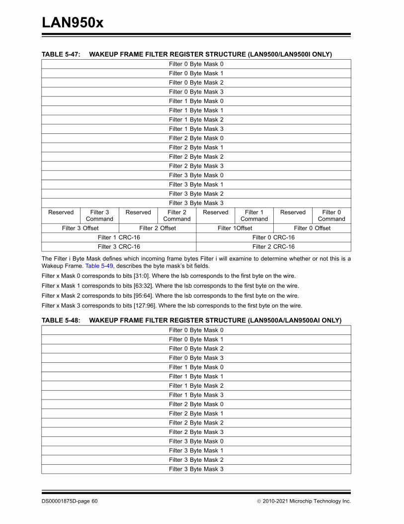
LAN950x
The Filter i Byte Mask defines which incoming frame bytes Filter i will examine to determine whether or not this is aWakeup Frame. Table 5-49, describes the byte mask’s bit fields.
Filter x Mask 0 corresponds to bits [31:0]. Where the lsb corresponds to the first byte on the wire.
Filter x Mask 1 corresponds to bits [63:32]. Where the lsb corresponds to the first byte on the wire.
Filter x Mask 2 corresponds to bits [95:64]. Where the lsb corresponds to the first byte on the wire.
Filter x Mask 3 corresponds to bits [127:96]. Where the lsb corresponds to the first byte on the wire.
TABLE 5-47: WAKEUP FRAME FILTER REGISTER STRUCTURE (LAN9500/LAN9500I ONLY)
Filter 0 Byte Mask 0
Filter 0 Byte Mask 1
Filter 0 Byte Mask 2
Filter 0 Byte Mask 3
Filter 1 Byte Mask 0
Filter 1 Byte Mask 1
Filter 1 Byte Mask 2
Filter 1 Byte Mask 3
Filter 2 Byte Mask 0
Filter 2 Byte Mask 1
Filter 2 Byte Mask 2
Filter 2 Byte Mask 3
Filter 3 Byte Mask 0
Filter 3 Byte Mask 1
Filter 3 Byte Mask 2
Filter 3 Byte Mask 3
Reserved Filter 3 Command
Reserved Filter 2 Command
Reserved Filter 1 Command
Reserved Filter 0 Command
Filter 3 Offset Filter 2 Offset Filter 1Offset Filter 0 Offset
Filter 1 CRC-16 Filter 0 CRC-16
Filter 3 CRC-16 Filter 2 CRC-16
TABLE 5-48: WAKEUP FRAME FILTER REGISTER STRUCTURE (LAN9500A/LAN9500AI ONLY)
Filter 0 Byte Mask 0
Filter 0 Byte Mask 1
Filter 0 Byte Mask 2
Filter 0 Byte Mask 3
Filter 1 Byte Mask 0
Filter 1 Byte Mask 1
Filter 1 Byte Mask 2
Filter 1 Byte Mask 3
Filter 2 Byte Mask 0
Filter 2 Byte Mask 1
Filter 2 Byte Mask 2
Filter 2 Byte Mask 3
Filter 3 Byte Mask 0
Filter 3 Byte Mask 1
Filter 3 Byte Mask 2
Filter 3 Byte Mask 3
DS00001875D-page 60 2010-2021 Microchip Technology Inc.
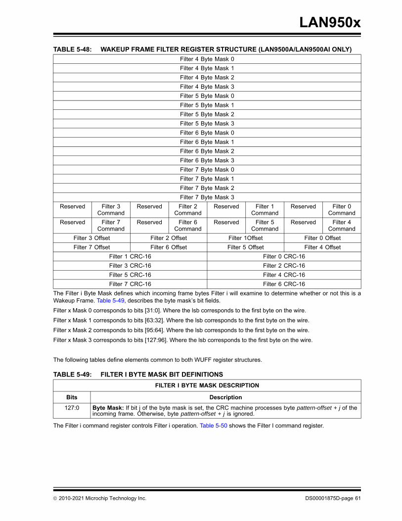
LAN950x
The Filter i Byte Mask defines which incoming frame bytes Filter i will examine to determine whether or not this is aWakeup Frame. Table 5-49, describes the byte mask’s bit fields.
Filter x Mask 0 corresponds to bits [31:0]. Where the lsb corresponds to the first byte on the wire.
Filter x Mask 1 corresponds to bits [63:32]. Where the lsb corresponds to the first byte on the wire.
Filter x Mask 2 corresponds to bits [95:64]. Where the lsb corresponds to the first byte on the wire.
Filter x Mask 3 corresponds to bits [127:96]. Where the lsb corresponds to the first byte on the wire.
The following tables define elements common to both WUFF register structures.
The Filter i command register controls Filter i operation. Table 5-50 shows the Filter I command register.
Filter 4 Byte Mask 0
Filter 4 Byte Mask 1
Filter 4 Byte Mask 2
Filter 4 Byte Mask 3
Filter 5 Byte Mask 0
Filter 5 Byte Mask 1
Filter 5 Byte Mask 2
Filter 5 Byte Mask 3
Filter 6 Byte Mask 0
Filter 6 Byte Mask 1
Filter 6 Byte Mask 2
Filter 6 Byte Mask 3
Filter 7 Byte Mask 0
Filter 7 Byte Mask 1
Filter 7 Byte Mask 2
Filter 7 Byte Mask 3
Reserved Filter 3 Command
Reserved Filter 2 Command
Reserved Filter 1 Command
Reserved Filter 0 Command
Reserved Filter 7 Command
Reserved Filter 6 Command
Reserved Filter 5 Command
Reserved Filter 4 Command
Filter 3 Offset Filter 2 Offset Filter 1Offset Filter 0 Offset
Filter 7 Offset Filter 6 Offset Filter 5 Offset Filter 4 Offset
Filter 1 CRC-16 Filter 0 CRC-16
Filter 3 CRC-16 Filter 2 CRC-16
Filter 5 CRC-16 Filter 4 CRC-16
Filter 7 CRC-16 Filter 6 CRC-16
TABLE 5-49: FILTER I BYTE MASK BIT DEFINITIONS
FILTER I BYTE MASK DESCRIPTION
Bits Description
127:0 Byte Mask: If bit j of the byte mask is set, the CRC machine processes byte pattern-offset + j of the incoming frame. Otherwise, byte pattern-offset + j is ignored.
TABLE 5-48: WAKEUP FRAME FILTER REGISTER STRUCTURE (LAN9500A/LAN9500AI ONLY)
2010-2021 Microchip Technology Inc. DS00001875D-page 61
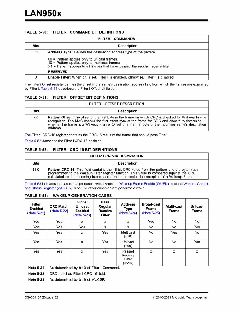
LAN950x
The Filter i Offset register defines the offset in the frame’s destination address field from which the frames are examinedby Filter i. Table 5-51 describes the Filter i Offset bit fields.
The Filter i CRC-16 register contains the CRC-16 result of the frame that should pass Filter i.
Table 5-52 describes the Filter i CRC-16 bit fields.
Table 5-53 indicates the cases that produce a wake when the Wakeup Frame Enable (WUEN) bit of the Wakeup Controland Status Register (WUCSR) is set. All other cases do not generate a wake.
Note 5-21 As determined by bit 0 of Filter i Command.
Note 5-22 CRC matches Filter i CRC-16 field.
Note 5-23 As determined by bit 9 of WUCSR.
TABLE 5-50: FILTER I COMMAND BIT DEFINITIONS
FILTER i COMMANDS
Bits Description
3:2 Address Type: Defines the destination address type of the pattern.
00 = Pattern applies only to unicast frames.10 = Pattern applies only to multicast frames.X1 = Pattern applies to all frames that have passed the regular receive filter.
1 RESERVED
0 Enable Filter: When bit is set, Filter i is enabled, otherwise, Filter i is disabled.
TABLE 5-51: FILTER I OFFSET BIT DEFINITIONS
FILTER I OFFSET DESCRIPTION
Bits Description
7:0 Pattern Offset: The offset of the first byte in the frame on which CRC is checked for Wakeup Frame recognition. The MAC checks the first offset byte of the frame for CRC and checks to determine whether the frame is a Wakeup Frame. Offset 0 is the first byte of the incoming frame's destination address.
TABLE 5-52: FILTER I CRC-16 BIT DEFINITIONS
FILTER I CRC-16 DESCRIPTION
Bits Description
15:0 Pattern CRC-16: This field contains the 16-bit CRC value from the pattern and the byte mask programmed to the Wakeup Filter register function. This value is compared against the CRC calculated on the incoming frame, and a match indicates the reception of a Wakeup Frame.
TABLE 5-53: WAKEUP GENERATION CASES
Filter Enabled
(Note 5-21)
CRC Match(Note 5-22)
Global Unicast Enabled
(Note 5-23)
Pass Regular Receive
Filter
Address Type
(Note 5-24)
Broad-cast Frame
(Note 5-25)
Multi-cast Frame
Unicast Frame
Yes Yes x x x Yes No No
Yes Yes Yes x x No No Yes
Yes Yes x Yes Multicast(=10)
No Yes No
Yes Yes x Yes Unicast(=00)
No No Yes
Yes Yes x Yes Passed Receive
Filter(=x1b)
x x x
DS00001875D-page 62 2010-2021 Microchip Technology Inc.
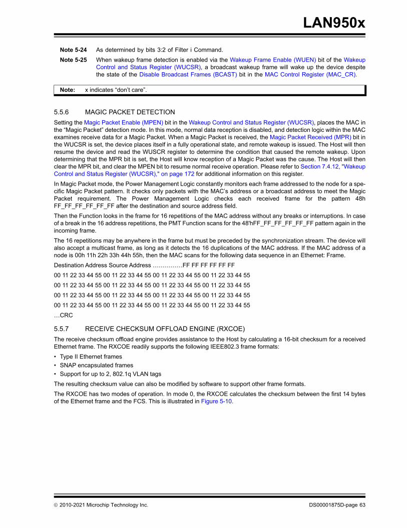
LAN950x
Note 5-24 As determined by bits 3:2 of Filter i Command.
Note 5-25 When wakeup frame detection is enabled via the Wakeup Frame Enable (WUEN) bit of the WakeupControl and Status Register (WUCSR), a broadcast wakeup frame will wake up the device despitethe state of the Disable Broadcast Frames (BCAST) bit in the MAC Control Register (MAC_CR).
5.5.6 MAGIC PACKET DETECTION
Setting the Magic Packet Enable (MPEN) bit in the Wakeup Control and Status Register (WUCSR), places the MAC inthe “Magic Packet” detection mode. In this mode, normal data reception is disabled, and detection logic within the MACexamines receive data for a Magic Packet. When a Magic Packet is received, the Magic Packet Received (MPR) bit inthe WUCSR is set, the device places itself in a fully operational state, and remote wakeup is issued. The Host will thenresume the device and read the WUSCR register to determine the condition that caused the remote wakeup. Upondetermining that the MPR bit is set, the Host will know reception of a Magic Packet was the cause. The Host will thenclear the MPR bit, and clear the MPEN bit to resume normal receive operation. Please refer to Section 7.4.12, "WakeupControl and Status Register (WUCSR)," on page 172 for additional information on this register.
In Magic Packet mode, the Power Management Logic constantly monitors each frame addressed to the node for a spe-cific Magic Packet pattern. It checks only packets with the MAC’s address or a broadcast address to meet the MagicPacket requirement. The Power Management Logic checks each received frame for the pattern 48hFF_FF_FF_FF_FF_FF after the destination and source address field.
Then the Function looks in the frame for 16 repetitions of the MAC address without any breaks or interruptions. In caseof a break in the 16 address repetitions, the PMT Function scans for the 48'hFF_FF_FF_FF_FF_FF pattern again in theincoming frame.
The 16 repetitions may be anywhere in the frame but must be preceded by the synchronization stream. The device willalso accept a multicast frame, as long as it detects the 16 duplications of the MAC address. If the MAC address of anode is 00h 11h 22h 33h 44h 55h, then the MAC scans for the following data sequence in an Ethernet: Frame.
Destination Address Source Address ……………FF FF FF FF FF FF
00 11 22 33 44 55 00 11 22 33 44 55 00 11 22 33 44 55 00 11 22 33 44 55
00 11 22 33 44 55 00 11 22 33 44 55 00 11 22 33 44 55 00 11 22 33 44 55
00 11 22 33 44 55 00 11 22 33 44 55 00 11 22 33 44 55 00 11 22 33 44 55
00 11 22 33 44 55 00 11 22 33 44 55 00 11 22 33 44 55 00 11 22 33 44 55
…CRC
5.5.7 RECEIVE CHECKSUM OFFLOAD ENGINE (RXCOE)
The receive checksum offload engine provides assistance to the Host by calculating a 16-bit checksum for a receivedEthernet frame. The RXCOE readily supports the following IEEE802.3 frame formats:
• Type II Ethernet frames
• SNAP encapsulated frames
• Support for up to 2, 802.1q VLAN tags
The resulting checksum value can also be modified by software to support other frame formats.
The RXCOE has two modes of operation. In mode 0, the RXCOE calculates the checksum between the first 14 bytesof the Ethernet frame and the FCS. This is illustrated in Figure 5-10.
Note: x indicates “don’t care”.
2010-2021 Microchip Technology Inc. DS00001875D-page 63
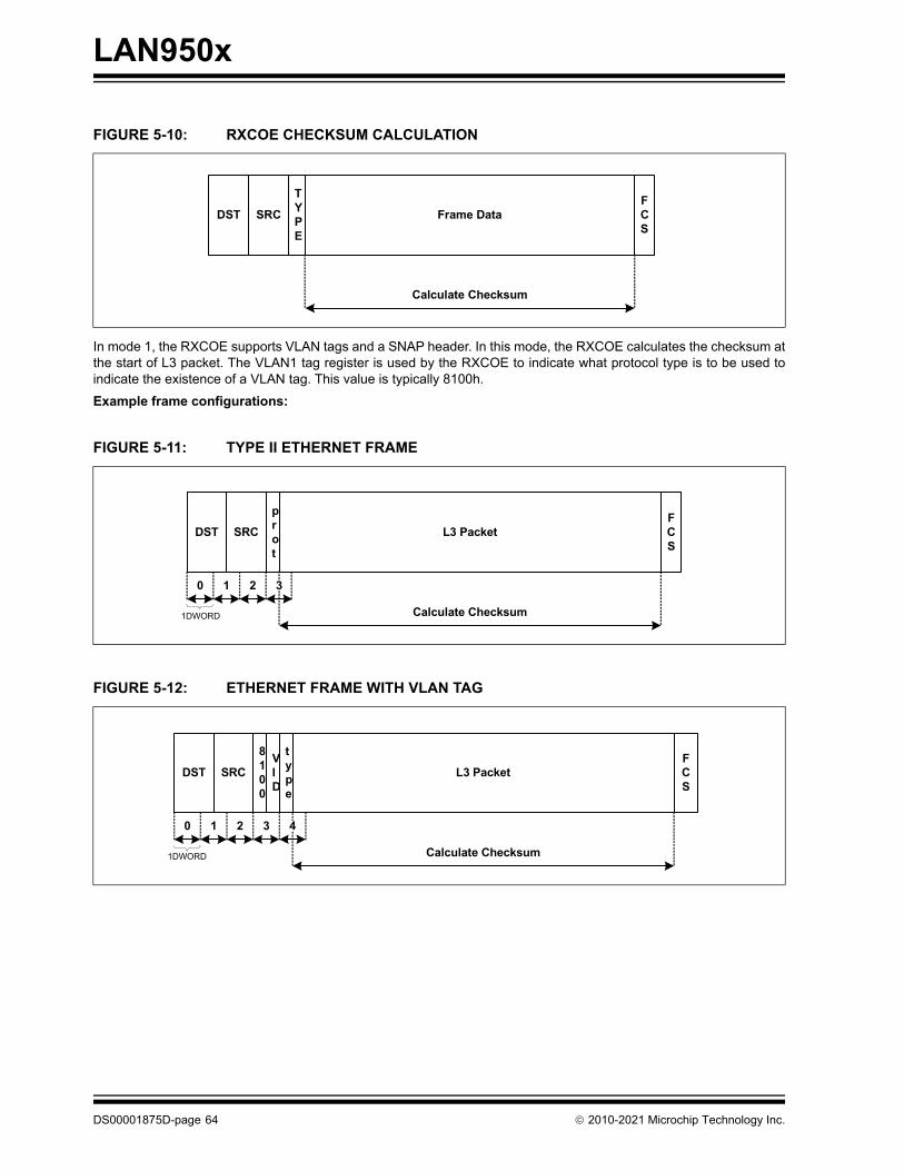
LAN950x
In mode 1, the RXCOE supports VLAN tags and a SNAP header. In this mode, the RXCOE calculates the checksum atthe start of L3 packet. The VLAN1 tag register is used by the RXCOE to indicate what protocol type is to be used toindicate the existence of a VLAN tag. This value is typically 8100h.
Example frame configurations:
FIGURE 5-10: RXCOE CHECKSUM CALCULATION
FIGURE 5-11: TYPE II ETHERNET FRAME
FIGURE 5-12: ETHERNET FRAME WITH VLAN TAG
DST SRC
TYPE
Frame DataFCS
Calculate Checksum
DST SRC
prot
0 1 2 3
L3 PacketFCS
Calculate Checksum1DWORD
DST SRC
8100
VID
0 1 2 3
type
4
L3 PacketFCS
Calculate Checksum1DWORD
DS00001875D-page 64 2010-2021 Microchip Technology Inc.
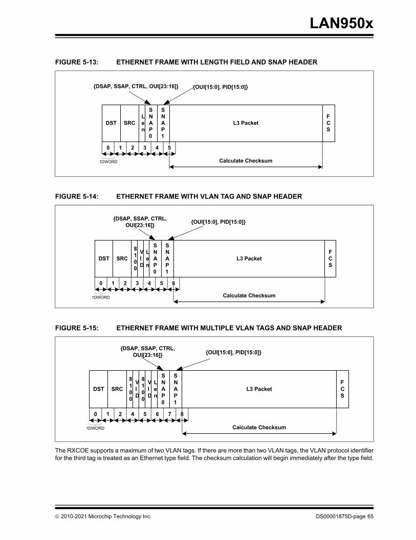
LAN950x
The RXCOE supports a maximum of two VLAN tags. If there are more than two VLAN tags, the VLAN protocol identifierfor the third tag is treated as an Ethernet type field. The checksum calculation will begin immediately after the type field.
FIGURE 5-13: ETHERNET FRAME WITH LENGTH FIELD AND SNAP HEADER
FIGURE 5-14: ETHERNET FRAME WITH VLAN TAG AND SNAP HEADER
FIGURE 5-15: ETHERNET FRAME WITH MULTIPLE VLAN TAGS AND SNAP HEADER
DST SRC L3 PacketFCS
SNAP0
SNAP1
Len
0 1 2
{DSAP, SSAP, CTRL, OUI[23:16]} {OUI[15:0], PID[15:0]}
3 4 5
Calculate Checksum1DWORD
DST SRC
8100
VID
L3 PacketFCS
SNAP0
SNAP1
3
Len
0 1 2
{DSAP, SSAP, CTRL, OUI[23:16]}
{OUI[15:0], PID[15:0]}
4 5 6
Calculate Checksum1DWORD
DST SRC
8100
VID
L3 PacketFCS
SNAP0
SNAP1
5
Len
0 1 2
{DSAP, SSAP, CTRL, OUI[23:16]} {OUI[15:0], PID[15:0]}
6 7 8
Calculate Checksum
8100
VID
4
1DWORD
2010-2021 Microchip Technology Inc. DS00001875D-page 65
LAN950x
The RXCOE resides in the RX path within the MAC. As the RXCOE receives an Ethernet frame, it calculates the 16-bitchecksum. The RXCOE passes the Ethernet frame to the RX FIFO with the checksum appended to the end of the frame.The RXCOE inserts the checksum immediately after the last byte of the Ethernet frame and before it transmits the statusword. The packet length field in the RX Status Word (refer to Section 5.4.1.2) will indicate that the frame size hasincreased by two bytes to accommodate the checksum.
Setting the RXCOE_EN bit in the Checksum Offload Engine Control Register (COE_CR) enables the RXCOE, while theRXCOE_MODE bit selects the operating mode. When the RXCOE is disabled, the received data is simply passedthrough the RXCOE unmodified.
Note 1: Software applications must stop the receiver and flush the RX data path before changing the state of theRXCOE_EN or RXCOE_MODE bits.
2: When the RXCOE is enabled, automatic pad stripping must be disabled (bit 8 (PADSTR) of the MAC ControlRegister (MAC_CR)) and vice versa. These functions cannot be enabled simultaneously.
5.5.7.1 RX Checksum Calculation
The checksum is calculated 16 bits at a time. In the case of an odd sized frame, an extra byte of zero is used to pad upto 16 bits.
Consider the following packet: DA, SA, Type, B0, B1, B2 … BN, FCS
Let [A, B] = A*256 + B;
If the packet has an even number of octets then
checksum = [B1, B0] + C0 + [B3, B2] + C1 + … + [BN, BN-1] + CN-1
Where C0, C1, ... CN-1 are the carry out results of the intermediate sums.
If the packet has an odd number of octets then
checksum = [B1, B0] + C0 + [B3, B2] + C1 + … + [0, BN] + CN-1
5.5.8 TRANSMIT CHECKSUM OFFLOAD ENGINE (TXCOE)
The transmit checksum offload engine provides assistance to the CPU by calculating a 16-bit checksum, typically forTCP, for a transmit Ethernet frame. The TXCOE calculates the checksum and inserts the results back into the datastream as it is transferred to the MAC.
To activate the TXCOE and perform a checksum calculation, the Host must first set the TX Checksum Offload EngineEnable (TX_COE_EN) bit in the Checksum Offload Engine Control Register (COE_CR). The Host then pre-pends a 3DWORD buffer to the data that will be transmitted. The pre-pended buffer includes a TX Command A, TX Command B,and a 32-bit TX checksum preamble (refer to Table 5-54). When the CK bit of the TX Command ‘B’ is set in conjunctionwith the FS bit of TX Command ‘A’ and the TX_COE_EN bit of the COE_CR register, the TXCOE will perform a check-sum calculation on the associated packet. The TX checksum preamble instructs the TXCOE on the handling of the asso-ciated packet. The TXCSSP - TX Checksum Start Pointer field of the TX checksum preamble defines the byte offset atwhich the data checksum calculation will begin. The checksum calculation will begin at this offset and will continue untilthe end of the packet. The data checksum calculation must not begin in the MAC header (first 14 bytes) or in the last 4bytes of the TX packet. When the calculation is complete, the checksum will be inserted into the packet at the byte offsetdefined by the TXCSLOC - TX Checksum Location field of the TX checksum preamble. The TX checksum cannot beinserted in the MAC header (first 14 bytes) or in the last 4 bytes of the TX packet. If the CK bit is not set in the first TXCommand ‘B’ of a packet, the packet is passed directly through the TXCOE without modification, regardless if theTXCOE_EN is set. An example of a TX packet with a pre-pended TX checksum preamble can be found in Section5.4.2.9, "TX Example 3". In this example, the Host provides the Ethernet frame to the Ethernet controller (via a USBpacket) in four fragments, the first containing the TX Checksum Preamble. Figure 5-8 shows how these fragments areloaded into the TX Data FIFO. For more information on the TX Command ‘A’ and TX Command ‘B’, refer to Section5.4.2.1, "TX Command Format," on page 47.
If the TX packet already includes a partial checksum calculation (perhaps inserted by an upper layer protocol), thischecksum can be included in the hardware checksum calculation by setting the TXCSSP field in the TX checksum pre-amble to include the partial checksum. The partial checksum can be replaced by the completed checksum calculationby setting the TXCSLOC pointer to point to the location of the partial checksum.
Note: When enabled, the RXCOE calculates a checksum for every received frame.
DS00001875D-page 66 2010-2021 Microchip Technology Inc.
LAN950x
Note 1: When the TXCOE is enabled, the third DWORD of the pre-pended packet is not transmitted. However, 4bytes must be added to the packet length field in TX Command B.
2: Software applications must stop the transmitter and flush the TX data path before changing the state of theTXCOE_EN bit. However, the CK bit of TX Command B can be set or cleared on a per-packet basis.
3: The TXCOE_MODE may only be changed if the TX path is disabled. If it is desired to change this valueduring run time, it is safe to do so only after the TX Ethernet path is disabled and the TLI is empty.
4: The TX checksum preamble must be DWORD-aligned.
5: TX preamble size is accounted for in both the buffer length and packet length.
6: The first buffer, which contains the TX preamble, may not contain any Ethernet frame data
FIGURE 5-16: TX Example Illustrating a Pre-pended TX Checksum Preamble on page 68 illustrates the use of a pre-pended checksum preamble when transmitting an Ethernet frame consisting of 3 payload buffers.
TABLE 5-54: TX CHECKSUM PREAMBLE
FIELD DESCRIPTION
31:28 RESERVED
27:16 TXCSLOC - TX Checksum LocationThis field specifies the byte offset where the TX checksum will be inserted in the TX packet. The checksum will replace two bytes of data starting at this offset.
Note: The TX checksum cannot be inserted in the MAC header (first 14 bytes) or in the last 4 bytes of the TX packet.
15:12 RESERVED
11:0 TXCSSP - TX Checksum Start PointerThis field indicates start offset, in bytes, where the checksum calculation will begin in the associated TX packet.
Note: The data checksum calculation must not begin in the MAC header (first 14 bytes) or in the last 4 bytes of the TX packet.
2010-2021 Microchip Technology Inc. DS00001875D-page 67
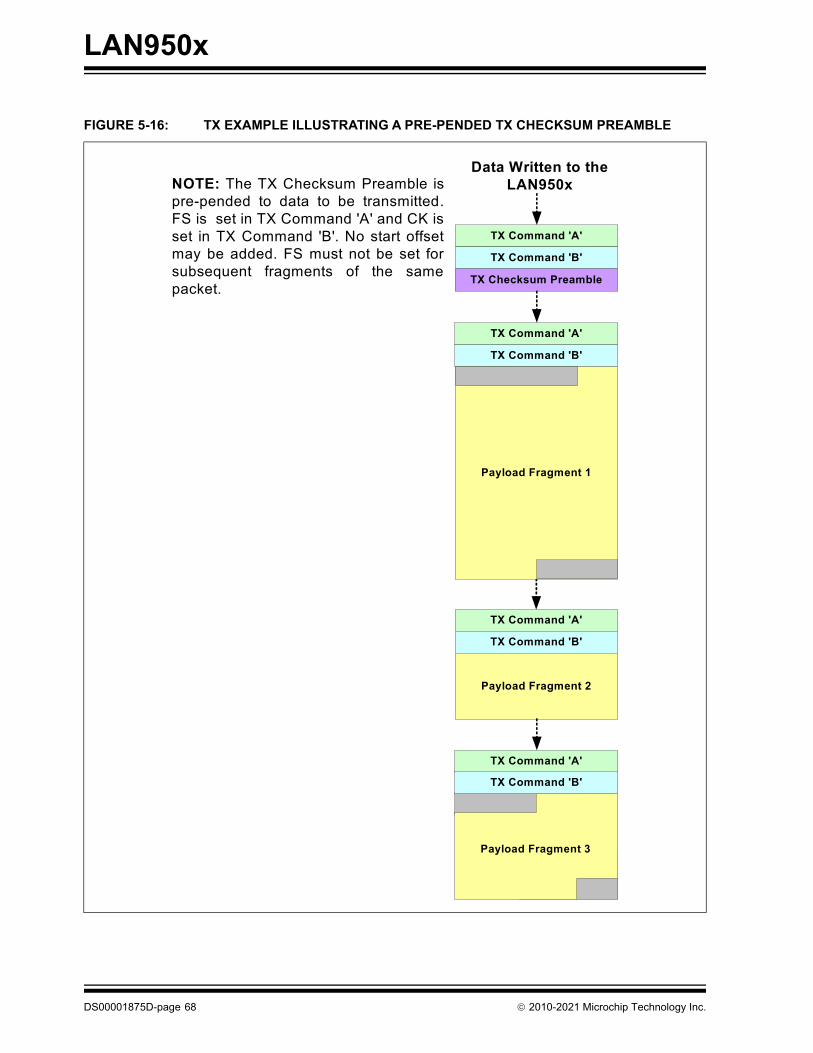
LAN950x
FIGURE 5-16: TX EXAMPLE ILLUSTRATING A PRE-PENDED TX CHECKSUM PREAMBLE
TX Command 'A'
Pad DWORD 1
TX Command 'A'
TX Command 'B'
10-ByteEnd Offset Padding
Payload Fragment 2
TX Command 'A'
TX Command 'B'
Data Written to the LAN950x
Payload Fragment 3
TX Command 'A'
TX Command 'B'
TX Checksum Preamble
NOTE: The TX Checksum Preamble is pre-pended to data to be transmitted. FS is set in TX Command 'A' and CK is set in TX Command 'B'. No start offset may be added. FS must not be set for subsequent fragments of the same packet.
TX Command 'B'
Payload Fragment 1
DS00001875D-page 68 2010-2021 Microchip Technology Inc.
LAN950x
5.5.8.1 TX Checksum Calculation
The TX checksum calculation is performed using the same operation as the RX checksum shown in Section 5.5.7.1,with the exception that the calculation starts as indicated by the preamble, and the transmitted checksum is the one’s-compliment of the final calculation.
5.5.9 MAC CONTROL AND STATUS REGISTERS (MCSR)
Please refer to Section 7.4, "MAC Control and Status Registers," on page 158 for a complete description of the MCSR.
5.6 10/100 Internal Ethernet PHY
The device integrates an IEEE 802.3 Physical Layer for Twisted Pair Ethernet applications. The PHY can be configuredfor either 100 Mbps (100Base-TX) or 10 Mbps (10Base-T) Ethernet operation in either Full or Half Duplex configura-tions. The PHY block includes auto-negotiation. Minimal external components are required for the utilization of the inter-nal PHY.
The device provides an option to use an external PHY in place of the internal PHY. The external PHY can be connectedvia the Media Independent Interface (MII) port. This option is useful for supporting Home PNA operations. When anexternal PHY is used, the internal PHY must be placed into general power down via a PHY reset (refer to Section 5.6.9,"PHY Resets," on page 78 for further information).
Functionally, the internal PHY can be divided into the following sections:
• 100Base-TX transmit and receive
• 10Base-T transmit and receive
• Internal MII interface to the Ethernet Media Access Controller
• Auto-negotiation to automatically determine the best speed and duplex possible
• Management Control to read status registers and write control registers
5.6.1 100BASE-TX TRANSMIT
The data path of the 100Base-TX is shown in Figure 5-17. Each major block is explained in the following sections.
Note: When the TX checksum offload feature is invoked, if the calculated checksum is 0000h, it is left unaltered.UDP checksums are optional under IPv4, and a zero checksum calculated by the TX checksum offloadfeature will erroneously indicate to the receiver that no checksum was calculated, however, the packet willtypically not be rejected by the receiver. Under IPv6, however, according to RFC 2460, the UDP checksumis not optional. A calculated checksum that yields a result of zero must be changed to FFFFh for insertioninto the UDP header. IPv6 receivers discard UDP packets containing a zero checksum. Thus, this featuremust not be used for UDP checksum calculation under IPv6.
2010-2021 Microchip Technology Inc. DS00001875D-page 69
LAN950x
5.6.1.1 4B/5B Encoding
The transmit data passes from the MII block to the 4B/5B encoder. This block encodes the data from 4-bit nibbles to 5-bit symbols (known as “code-groups”) according to Table 5-55. Each 4-bit data-nibble is mapped to 16 of the 32 possiblecode-groups. The remaining 16 code-groups are either used for control information or are not valid.
The first 16 code-groups are referred to by the hexadecimal values of their corresponding data nibbles, 0 through F. Theremaining code-groups are given letter designations with slashes on either side. For example, an IDLE code-group is/I/, a transmit error code-group is /H/, etc.
The encoding process may be bypassed by clearing bit 6 of register 31. When the encoding is bypassed the 5th transmitdata bit is equivalent to TX_ER.
FIGURE 5-17: 100BASE-TX DATA PATH
TABLE 5-55: 4B/5B CODE TABLE
Code Group SYM Receiver Interpretation Transmitter Interpretation
11110 0 0 0000 DATA 0 0000 DATA
01001 1 1 0001 1 0001
10100 2 2 0010 2 0010
10101 3 3 0011 3 0011
01010 4 4 0100 4 0100
01011 5 5 0101 5 0101
01110 6 6 0110 6 0110
01111 7 7 0111 7 0111
10010 8 8 1000 8 1000
10011 9 9 1001 9 1001
10110 A A 1010 A 1010
10111 B B 1011 B 1011
11010 C C 1100 C 1100
11011 D D 1101 D 1101
11100 E E 1110 E 1110
MAC
Tx Driver
MLT-3 Converter
NRZI Converter
4B/5B Encoder
Magnetics
CAT-5RJ45
100M PLL
Internal MII 25 MHz by 4 bits
TX_CLK
25MHz by5 bits
NRZI
MLT-3
MLT-3
MLT-3
MLT-3
Scrambler and PISO
125 Mbps Serial
MII 25MHzby 4 bits
DS00001875D-page 70 2010-2021 Microchip Technology Inc.
LAN950x
5.6.1.2 Scrambling
Repeated data patterns (especially the IDLE code-group) can have power spectral densities with large narrow-bandpeaks. Scrambling the data helps eliminate these peaks and spread the signal power more uniformly over the entirechannel bandwidth. This uniform spectral density is required by FCC regulations to prevent excessive EMI from beingradiated by the physical wiring.
The scrambler also performs the Parallel In Serial Out conversion (PISO) of the data.
5.6.1.3 NRZI and MLT3 Encoding
The scrambler block passes the 5-bit wide parallel data to the NRZI converter where it becomes a serial 125MHz NRZIdata stream. The NRZI is encoded to MLT-3. MLT3 is a tri-level code where a change in the logic level represents a codebit “1” and the logic output remaining at the same level represents a code bit “0”.
5.6.1.4 100M Transmit Driver
The MLT3 data is then passed to the analog transmitter, which launches the differential MLT-3 signal, on outputs TXPand TXN, to the twisted pair media via a 1:1 ratio isolation transformer. The 10Base-T and 100Base-TX signals passthrough the same transformer so that common “magnetics” can be used for both. The transmitter drives into the 100impedance of the CAT-5 cable. Cable termination and impedance matching require external components.
5.6.1.5 100M Phase Lock Loop (PLL)
The 100M PLL locks onto reference clock and generates the 125MHz clock used to drive the 125 MHz logic and the100Base-Tx Transmitter.
5.6.2 100BASE-TX RECEIVE
The receive data path is shown in Figure 5-18. Detailed descriptions are given in the following subsections.
11101 F F 1111 F 1111
11111 I IDLE Sent after /T/R until TX_EN
11000 J First nibble of SSD, translated to “0101” following IDLE, else RX_ER
Sent for rising TX_EN
10001 K Second nibble of SSD, translated to “0101” following J, else RX_ER
Sent for rising TX_EN
01101 T First nibble of ESD, causes de-assertion of CRS if followed by /R/, else assertion of RX_ER
Sent for falling TX_EN
00111 R Second nibble of ESD, causes deassertion of CRS if following /T/, else assertion of RX_ER
Sent for falling TX_EN
00100 H Transmit Error Symbol Sent for rising TX_ER
00110 V INVALID, RX_ER if during RX_DV INVALID
11001 V INVALID, RX_ER if during RX_DV INVALID
00000 V INVALID, RX_ER if during RX_DV INVALID
00001 V INVALID, RX_ER if during RX_DV INVALID
00010 V INVALID, RX_ER if during RX_DV INVALID
00011 V INVALID, RX_ER if during RX_DV INVALID
00101 V INVALID, RX_ER if during RX_DV INVALID
01000 V INVALID, RX_ER if during RX_DV INVALID
01100 V INVALID, RX_ER if during RX_DV INVALID
10000 V INVALID, RX_ER if during RX_DV INVALID
TABLE 5-55: 4B/5B CODE TABLE (CONTINUED)
Code Group SYM Receiver Interpretation Transmitter Interpretation
2010-2021 Microchip Technology Inc. DS00001875D-page 71
LAN950x
5.6.2.1 100M Receive Input
The MLT-3 from the cable is fed into the PHY (on inputs RXP and RXN) via a 1:1 ratio transformer. The ADC samplesthe incoming differential signal at a rate of 125M samples per second. Using a 64-level quanitizer, it generates 6 digitalbits to represent each sample. The DSP adjusts the gain of the ADC according to the observed signal levels such thatthe full dynamic range of the ADC can be used
5.6.2.2 Equalizer, Baseline Wander Correction and Clock and Data Recovery
The 6 bits from the ADC are fed into the DSP block. The equalizer in the DSP section compensates for phase and ampli-tude distortion caused by the physical channel consisting of magnetics, connectors, and CAT- 5 cable. The equalizercan restore the signal for any good-quality CAT-5 cable between 1m and 150m.
If the DC content of the signal is such that the low-frequency components fall below the low frequency pole of the iso-lation transformer, then the droop characteristics of the transformer will become significant and Baseline Wander (BLW)on the received signal will result. To prevent corruption of the received data, the PHY corrects for BLW and can receivethe ANSI X3.263-1995 FDDI TP-PMD defined “killer packet” with no bit errors.
The 100M PLL generates multiple phases of the 125MHz clock. A multiplexer, controlled by the timing unit of the DSP,selects the optimum phase for sampling the data. This is used as the received recovered clock. This clock is used toextract the serial data from the received signal.
5.6.2.3 NRZI and MLT-3 Decoding
The DSP generates the MLT-3 recovered levels that are fed to the MLT-3 converter. The MLT-3 is then converted to anNRZI data stream.
5.6.2.4 Descrambling
The descrambler performs an inverse function to the scrambler in the transmitter and also performs the Serial In ParallelOut (SIPO) conversion of the data.
During reception of IDLE (/I/) symbols. the descrambler synchronizes its descrambler key to the incoming stream. Oncesynchronization is achieved, the descrambler locks on this key and is able to descramble incoming data.
FIGURE 5-18: RECEIVE DATA PATH
MAC
A/D Converter
MLT-3 Converter
NRZI Converter
4B/5B Decoder
Magnetics CAT-5RJ45
100M PLL
InternalMII 25MHz by 4 bits
RX_CLK
25MHz by5 bits
NRZI
MLT-3MLT-3 MLT-3
6 bit Data
Descrambler and SIPO
125 Mbps Serial
DSP: Timing recovery, Equalizer and BLW Correction
MLT-3
MII 25MHzby 4 bits
DS00001875D-page 72 2010-2021 Microchip Technology Inc.
LAN950x
Special logic in the descrambler ensures synchronization with the remote PHY by searching for IDLE symbols within awindow of 4000 bytes (40us). This window ensures that a maximum packet size of 1514 bytes, allowed by the IEEE802.3 standard, can be received with no interference. If no IDLE-symbols are detected within this time-period, receiveoperation is aborted and the descrambler re-starts the synchronization process.
The descrambler can be bypassed by setting bit 0 of register 31.
5.6.2.5 Alignment
The de-scrambled signal is then aligned into 5-bit code-groups by recognizing the /J/K/ Start-of-Stream Delimiter (SSD)pair at the start of a packet. Once the code-word alignment is determined, it is stored and utilized until the next start offrame.
5.6.2.6 5B/4B Decoding
The 5-bit code-groups are translated into 4-bit data nibbles according to the 4B/5B table. The SSD, /J/K/, is translatedto “0101 0101” as the first 2 nibbles of the MAC preamble. Reception of the SSD causes the PHY to assert the internalRX_DV signal, indicating that valid data is available on the Internal RXD bus. Successive valid code-groups are trans-lated to data nibbles. Reception of either the End of Stream Delimiter (ESD) consisting of the /T/R/ symbols, or at leasttwo /I/ symbols causes the PHY to de-assert the internal carrier sense and RX_DV.
These symbols are not translated into data.
5.6.2.7 Receiver Errors
bit During a frame, unexpected code-groups are considered receive errors. Expected code groups are the DATA set (0 through F), and the /T/R/ (ESD) symbol pair. When a receive error occurs, the internal MII’s RX_ER signal is asserted and arbitrary data is driven onto the internal receive data bus (RXD) to the MAC. Should an error be detected during the time that the /J/K/ delimiter is being decoded (bad SSD error), RX_ER is asserted and the value 1110b is driven onto the internal receive data bus (RXD) to the MAC. Note that the internal MII’s data valid signal (RX_DV) is not yet asserted when the bad SSD occurs.
5.6.3 10BASE-T TRANSMIT
Data to be transmitted comes from the MAC layer controller. The 10Base-T transmitter receives 4-bit nibbles from theMII at a rate of 2.5MHz and converts them to a 10Mbps serial data stream. The data stream is then Manchester encodedand sent to the analog transmitter, which drives a signal onto the twisted pair via the external magnetics.
The 10M transmitter uses the following blocks:
• MII (digital)
• TX 10M (digital)
• 10M Transmitter (analog)
• 10M PLL (analog)
5.6.3.1 10M Transmit Data Across the Internal MII Bus
The MAC controller drives the transmit data onto the internal TXD BUS. When the controller has driven TX_EN high toindicate valid data, the data is latched by the MII block on the rising edge of TX_CLK. The data is in the form of 4-bitwide 2.5MHz data.
5.6.3.2 Manchester Encoding
The 4-bit wide data is sent to the TX10M block. The nibbles are converted to a 10Mbps serial NRZI data stream. The10M PLL locks onto the external clock or internal oscillator and produces a 20MHz clock. This is used to Manchesterencode the NRZ data stream. When no data is being transmitted (TX_EN is low), the TX10M block outputs Normal LinkPulses (NLPs) to maintain communications with the remote link partner.
5.6.3.3 10M Transmit Drivers
The Manchester encoded data is sent to the analog transmitter where it is shaped and filtered before being driven outas a differential signal across the TXP and TXN outputs.
2010-2021 Microchip Technology Inc. DS00001875D-page 73
LAN950x
5.6.4 10BASE-T RECEIVE
The 10Base-T receiver gets the Manchester encoded analog signal from the cable via the magnetics. It recovers thereceive clock from the signal and uses this clock to recover the NRZI data stream. This 10M serial data is converted to4-bit data nibbles which are passed to the controller across the MII at a rate of 2.5MHz.
This 10M receiver uses the following blocks:
• Filter and SQUELCH (analog)
• 10M PLL (analog)
• RX 10M (digital)
• MII (digital)
5.6.4.1 10M Receive Input and Squelch
The Manchester signal from the cable is fed into the PHY (on inputs RXP and RXN) via 1:1 ratio magnetics. It is firstfiltered to reduce any out-of-band noise. It then passes through a SQUELCH circuit. The SQUELCH is a set of amplitudeand timing comparators that normally reject differential voltage levels below 300mV and detect and recognize differentialvoltages above 585mV.
5.6.4.2 Manchester Decoding
The output of the SQUELCH goes to the RX10M block where it is validated as Manchester encoded data. The polarityof the signal is also checked. If the polarity is reversed (local RXP is connected to RXN of the remote partner and viceversa), then this is identified and corrected. The reversed condition is indicated by the flag “XPOL“, bit 4 in register 27.The 10M PLL is locked onto the received Manchester signal and from this, generates the received 20MHz clock. Usingthis clock, the Manchester encoded data is extracted and converted to a 10MHz NRZI data stream. It is then convertedfrom serial to 4-bit wide parallel data.
The RX10M block also detects valid 10Base-T IDLE signals - Normal Link Pulses (NLPs) - to maintain the link.
5.6.4.3 Jabber Detection
Jabber is a condition in which a station transmits for a period of time longer than the maximum permissible packet length,usually due to a fault condition, that results in holding the TX_EN input for a long period. Special logic is used to detectthe jabber state and abort the transmission to the line, within 45 mS. Once TX_EN is deasserted, the logic resets thejabber condition.
5.6.5 AUTO-NEGOTIATION
The purpose of the Auto-negotiation function is to automatically configure the PHY to the optimum link parametersbased on the capabilities of its link partner. Auto-negotiation is a mechanism for exchanging configuration informationbetween two link-partners and automatically selecting the highest performance mode of operation supported by bothsides. Auto-negotiation is fully defined in clause 28 of the IEEE 802.3 specification.
Once auto-negotiation has completed, information about the resolved link can be passed back to the controller via theinternal Serial Management Interface (SMI). The results of the negotiation process are reflected in the Speed Indicationbits in register 31, as well as the Link Partner Ability Register (Register 5).
The auto-negotiation protocol is a purely physical layer activity and proceeds independently of the MAC controller.
The advertised capabilities of the PHY are stored in register 4 of the SMI registers. The default advertised by the PHYis determined by user-defined on-chip signal options.
The following blocks are activated during an Auto-negotiation session:
• Auto-negotiation (digital)
• 100M ADC (analog)
• 100M PLL (analog)
• 100M equalizer/BLW/clock recovery (DSP)
• 10M SQUELCH (analog)
• 10M PLL (analog)
• 10M Transmitter (analog)
DS00001875D-page 74 2010-2021 Microchip Technology Inc.
LAN950x
When enabled, auto-negotiation is started by the occurrence of one of the following events:
• Hardware reset
• Software reset
• Power-down reset
• Link status down
• Setting register 0, bit 9 high (auto-negotiation restart)
On detection of one of these events, the PHY begins auto-negotiation by transmitting bursts of Fast Link Pulses (FLP).These are bursts of link pulses from the 10M transmitter. They are shaped as Normal Link Pulses and can pass uncor-rupted down CAT-3 or CAT-5 cable. A Fast Link Pulse Burst consists of up to 33 pulses. The 17 odd-numbered pulses,which are always present, frame the FLP burst. The 16 even-numbered pulses, which may be present or absent, containthe data word being transmitted. Presence of a data pulse represents a “1”, while absence represents a “0”.
The data transmitted by an FLP burst is known as a “Link Code Word.” These are defined fully in IEEE 802.3 clause 28.In summary, the PHY advertises 802.3 compliance in its selector field (the first 5 bits of the Link Code Word). It adver-tises its technology ability according to the bits set in register 4 of the SMI registers.
There are 4 possible matches of the technology abilities. In the order of priority these are:
• 100M full-duplex (Highest priority)
• 100M half-duplex
• 10M full-duplex
• 10M half-duplex
If the full capabilities of the PHY are advertised (100M, full-duplex), and if the link partner is capable of 10M and 100M,then auto-negotiation selects 100M as the highest performance mode. If the link partner is capable of half and full-duplexmodes, then auto-negotiation selects full-duplex as the highest performance operation.
Once a capability match has been determined, the link code words are repeated with the acknowledge bit set. Any dif-ference in the main content of the link code words at this time will cause auto-negotiation to re-start. Auto-negotiationwill also re-start if not all of the required FLP bursts are received.
Writing register 4 bits [8:5] allows software control of the capabilities advertised by the PHY. Writing register 4 does notautomatically re-start auto-negotiation. Register 0, bit 9 must be set before the new abilities will be advertised. Auto-negotiation can also be disabled via software by clearing register 0, bit 12.
The device does not support “Next Page” capability.
5.6.6 PARALLEL DETECTION
If LAN950x is connected to a device lacking the ability to auto-negotiate (i.e. no FLPs are detected), it is able to deter-mine the speed of the link based on either 100M MLT-3 symbols or 10M Normal Link Pulses. In this case the link ispresumed to be half-duplex per the IEEE standard. This ability is known as “Parallel Detection. This feature ensuresinteroperability with legacy link partners. If a link is formed via parallel detection, then bit 0 in register 6 is cleared toindicate that the Link Partner is not capable of auto-negotiation. The Ethernet MAC has access to this information viathe management interface. If a fault occurs during parallel detection, bit 4 of register 6 is set.
Register 5 is used to store the Link Partner Ability information, which is coded in the received FLPs. If the Link Partneris not auto-negotiation capable, then register 5 is updated after completion of parallel detection to reflect the speed capa-bility of the Link Partner.
5.6.6.1 Re-starting Auto-negotiation
Auto-negotiation can be re-started at any time by setting register 0, bit 9. Auto-negotiation will also re-start if the link isbroken at any time. A broken link is caused by signal loss. This may occur because of a cable break, or because of aninterruption in the signal transmitted by the Link Partner. Auto-negotiation resumes in an attempt to determine the newlink configuration.
If the management entity re-starts Auto-negotiation by writing to bit 9 of the control register, the device will respond bystopping all transmission/receiving operations. Once the break_link_timer is done, in the Auto-negotiation state-machine (approximately 1200 mS) the auto-negotiation will re-start. The Link Partner will have also dropped the link dueto lack of a received signal, so it too will resume auto-negotiation.
2010-2021 Microchip Technology Inc. DS00001875D-page 75
LAN950x
5.6.6.2 Disabling Auto-negotiation
Auto-negotiation can be disabled by setting register 0, bit 12 to zero. The device will then force its speed of operationto reflect the information in register 0, bit 13 (speed) and register 0, bit 8 (duplex). The speed and duplex bits in register0 should be ignored when auto-negotiation is enabled.
5.6.6.3 Half vs. Full-Duplex
Half-duplex operation relies on the CSMA/CD (Carrier Sense Multiple Access / Collision Detect) protocol to handle net-work traffic and collisions. In this mode, the internal carrier sense signal, CRS, responds to both transmit and receiveactivity. In this mode, If data is received while the PHY is transmitting, a collision results.
In full-duplex mode, the PHY is able to transmit and receive data simultaneously. In this mode, the internal CRSresponds only to receive activity. The CSMA/CD protocol does not apply and collision detection is disabled.
Table 5-56 describes the behavior of the internal CRS bit under all receive/transmit conditions.
The internal CRS signal is used to trigger bit 10 (No Carrier) of the TX Status Word (See Section 5.4.2.6, "TX StatusFormat," on page 50). The CRS value, and subsequently the No Carrier value, are invalid during any full-duplex trans-mission. Therefore, these signals cannot be used as a verification method of transmitted packets when transmitting in10/100 Mbps full-duplex modes.
Note 5-1 The device’s 10/100 PHY internal CRS signal operates in two modes: Active and Low. When in Activemode, the internal CRS will transition high and low upon line activity, where a high value indicates acarrier has been detected. In Low mode, the internal CRS stays low and does not indicate carrierdetection. The internal CRS signal and No Carrier (bit 10 of the TX Status Word) cannot be used asa verification method of transmitted packets when transmitting in 10/100 Mbps full-duplex mode.
5.6.7 HP AUTO-MDIX
HP Auto-MDIX facilitates the use of CAT-3 (10 BASE-T) or CAT-5 (100 BASE-T) media UTP interconnect cable withoutconsideration of interface wiring scheme. If a user plugs in either a direct connect LAN cable, or a cross-over patchcable, as shown in Figure 5-19, the device’s Auto-MDIX PHY is capable of configuring the TPO and TPI twisted pairpins for correct transceiver operation.
The internal logic of the device detects the TX and RX pins of the connecting device. Since the RX and TX line pairsare interchangeable, special PCB design considerations are needed to accommodate the symmetrical magnetics andtermination of an Auto-MDIX design.
TABLE 5-56: CRS BEHAVIOR
Mode Speed Duplex ActivityCRS Behavior
(Note 5-1)
Manual 10 Mbps Half-Duplex Transmitting Active
Manual 10 Mbps Half-Duplex Receiving Active
Manual 10 Mbps Full-Duplex Transmitting Low
Manual 10 Mbps Full-Duplex Receiving Active
Manual 100 Mbps Half-Duplex Transmitting Active
Manual 100 Mbps Half-Duplex Receiving Active
Manual 100 Mbps Full-Duplex Transmitting Low
Manual 100 Mbps Full-Duplex Receiving Active
Auto-Negotiation 10 Mbps Half-Duplex Transmitting Active
Auto-Negotiation 10 Mbps Half-Duplex Receiving Active
Auto-Negotiation 10 Mbps Full-Duplex Transmitting Low
Auto-Negotiation 10 Mbps Full-Duplex Receiving Active
Auto-Negotiation 100 Mbps Half-Duplex Transmitting Active
Auto-Negotiation 100 Mbps Half-Duplex Receiving Active
Auto-Negotiation 100 Mbps Full-Duplex Transmitting Low
Auto-Negotiation 100 Mbps Full-Duplex Receiving Active
DS00001875D-page 76 2010-2021 Microchip Technology Inc.
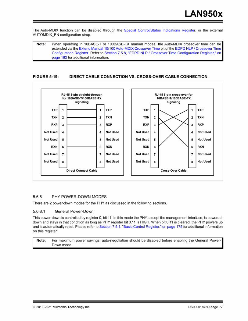
LAN950x
The Auto-MDIX function can be disabled through the Special Control/Status Indications Register, or the externalAUTOMDIX_EN configuration strap.
5.6.8 PHY POWER-DOWN MODES
There are 2 power-down modes for the PHY as discussed in the following sections.
5.6.8.1 General Power-Down
This power-down is controlled by register 0, bit 11. In this mode the PHY, except the management interface, is powered-down and stays in that condition as long as PHY register bit 0.11 is HIGH. When bit 0.11 is cleared, the PHY powers upand is automatically reset. Please refer to Section 7.5.1, "Basic Control Register," on page 175 for additional informationon this register.
Note: When operating in 10BASE-T or 100BASE-TX manual modes, the Auto-MDIX crossover time can beextended via the Extend Manual 10/100 Auto-MDIX Crossover Time bit of the EDPD NLP / Crossover TimeConfiguration Register. Refer to Section 7.5.8, "EDPD NLP / Crossover Time Configuration Register," onpage 182 for additional information.
FIGURE 5-19: DIRECT CABLE CONNECTION VS. CROSS-OVER CABLE CONNECTION.
Note: For maximum power savings, auto-negotiation should be disabled before enabling the General Power-Down mode.
1
2
3
4
5
6
7
8
TXP
TXN
RXP
Not Used
Not Used
RXN
Not Used
Not Used
1
2
3
4
5
6
7
8
TXP
TXN
RXP
Not Used
Not Used
RXN
Not Used
Not Used
Direct Connect Cable
RJ-45 8-pin straight-through for 10BASE-T/100BASE-TX
signaling
1
2
3
4
5
6
7
8
TXP
TXN
RXP
Not Used
Not Used
RXN
Not Used
Not Used
1
2
3
4
5
6
7
8
TXP
TXN
RXP
Not Used
Not Used
RXN
Not Used
Not Used
Cross-Over Cable
RJ-45 8-pin cross-over for 10BASE-T/100BASE-TX
signaling
2010-2021 Microchip Technology Inc. DS00001875D-page 77
LAN950x
5.6.8.2 Energy Detect Power-Down (EDPD)
This power-down mode is activated by setting the EDPWRDOWN bit of the Mode Control/Status Register. In this mode,when no energy is present on the line, the PHY is powered down (except the for the management interface, theSQUELCH circuit, and the ENERGYON logic). The ENERGYON logic is used to detect the presence of valid energyfrom 100BASE-TX, 10BASE-T, or Auto-negotiation signals.
In this mode, when the ENERGYON bit of the Mode Control/Status Register is low, the PHY is powered-down and noth-ing is transmitted. When energy is received via link pulses or packets, the ENERGYON bit goes high and the PHY pow-ers-up. The PHY automatically resets itself into the state prior to power-down and asserts the INT7 bit of the PHYInterrupt Source Flag Register register. If the ENERGYON interrupt is enabled, this event will cause a PHY interrupt tothe Interrupt Controller and the power management event detection logic. The first and possibly the second packet toactivate ENERGYON may be lost.
When THE EDPWRDOWN bit of the Mode Control/Status Register is low, energy detect power-down is disabled.
When in EDPD mode, the device’s NLP characteristics may be modified. The device can be configured to transmit NLPsin EDPD via the EDPD TX NLP Enable bit of the EDPD NLP / Crossover Time Configuration Register. When enabled,the TX NLP time interval is configurable via the EDPD TX NLP Interval Timer Select field of the EDPD NLP / CrossoverTime Configuration Register. When in EDPD mode, the device can also be configured to wake on the reception of oneor two NLPs. Setting the EDPD RX Single NLP Wake Enable bit of the EDPD NLP / Crossover Time Configuration Reg-ister will enable the device to wake on reception of a single NLP. If the EDPD RX Single NLP Wake Enable bit is cleared,the maximum interval for detecting reception of two NLPs to wake from EDPD is configurable via the EDPD RX NLPMax Interval Detect Select field of the EDPD NLP / Crossover Time Configuration Register.
5.6.9 PHY RESETS
In addition to a chip-level reset, the PHY supports two software-initiated resets. These are discussed in the followingsections.
5.6.9.1 PHY Soft Reset via PMT_CTL Register PHY Reset (PHY_RST) Bit
The PHY soft reset is initiated by writing a ‘1’ to the PHY Reset (PHY_RST) bit of the Power Management Control Reg-ister (PMT_CTL). This self-clearing bit will return to ‘0’ after approximately 2ms, at which time the PHY reset is complete.
5.6.9.2 PHY Soft Reset via PHY Basic Control Register Bit 15 (PHY Reg. 0.15)
The PHY Reg. 0.15 Soft Reset is initiated by writing a ‘1’ to bit 15 of the PHY’s Basic Control Register. This self-clearingbit will return to ‘0’ after approximately 256s, at which time the PHY reset is complete. The BCR reset initializes thelogic within the PHY, with the exception of register bits marked as NASR (Not Affected by Software Reset).
5.6.10 REQUIRED ETHERNET MAGNETICS
The magnetics selected for use with the device should be an Auto-MDIX style magnetic available from several vendors.The user is urged to review Application Note 8.13 “Suggested Magnetics” for the latest qualified and suggested mag-netics. Vendors and part numbers are provided in this application note.
5.6.11 PHY REGISTERS
Please refer to Section 7.5, "PHY Registers," on page 174 for a complete description of the PHY registers.
5.7 EEPROM Controller (EPC)
The device may use an external EEPROM to store the default values for the USB descriptors and the MAC address.The EEPROM controller supports most “93C46” type EEPROMs. The EEP_SIZE strap selects the size of the EEPROMattached to the device. When this strap is set to “0”, a 128 byte EEPROM is attached and a total of seven address bitsare used. When this strap is set to “1” a 256/512 byte EEPROM is attached and a total of nine address bits are used.
Note: A 3-wire style 1K/2K/4K EEPROM that is organized for 128 x 8-bit or 256/512 x 8-bit operation must beused.
DS00001875D-page 78 2010-2021 Microchip Technology Inc.
LAN950x
The MAC address is used as the default Ethernet MAC address and is loaded into the MAC’s ADDRH and ADDRL reg-isters. If a properly configured EEPROM is not detected, it is the responsibility of the Host LAN Driver to set the IEEEaddresses.
After a system-level reset occurs, the device will load the default values from a properly configured EEPROM. Thedevice will not accept USB transactions from the Host until this process is completed.
The EEPROM controller also allows the Host system to read, write and erase the contents of the Serial EEPROM.
5.7.1 EEPROM FORMAT
Table 5-57 illustrates the format in which data is stored inside of the EEPROM.
Note the EEPROM offsets are given in units of 16-bit word offsets. A length field with a value of zero indicates that thefield does not exist in the EEPROM. The device will use the field’s HW default value in this case.
Note 1: For the device descriptor, the only valid values for the length are 0 and 18.
2: For the configuration and interface descriptor, the only valid values for the length are 0 and 18.
3: The EEPROM programmer must ensure that if a string descriptor does not exist in the EEPROM, the refer-encing descriptor must contain 00h for the respective string index field.
4: If all string descriptor lengths are zero, then a Language ID will not be supported.
TABLE 5-57: EEPROM FORMAT
EEPROM Address EEPROM Contents
00h 0xA5
01h MAC Address [7:0]
02h MAC Address [15:8]
03h MAC Address [23:16]
04h MAC Address [31:24]
05h MAC Address [39:32]
06h MAC Address [47:40]
07h Full-Speed Polling Interval for Interrupt Endpoint
08h Hi-Speed Polling Interval for Interrupt Endpoint
09h Configuration Flags
0Ah Language ID Descriptor [7:0]
0Bh Language ID Descriptor [15:8]
0Ch Manufacturer ID String Descriptor Length (bytes)
0Dh Manufacturer ID String Descriptor EEPROM Word Offset
0Eh Product Name String Descriptor Length (bytes)
0Fh Product Name String Descriptor EEPROM Word Offset
10h Serial Number String Descriptor Length (bytes)
11h Serial Number String Descriptor EEPROM Word Offset
12h Configuration String Descriptor Length (bytes)
13h Configuration String Descriptor Word Offset
14h Interface String Descriptor Length (bytes)
15h Interface String Descriptor Word Offset
16h Hi-Speed Device Descriptor Length (bytes)
17h Hi-Speed Device Descriptor Word Offset
18h Hi-Speed Configuration and Interface Descriptor Length (bytes)
19h Hi-Speed Configuration and Interface Descriptor Word Offset
1Ah Full-Speed Device Descriptor Length (bytes)
1Bh Full-Speed Device Descriptor Word Offset
1Ch Full-Speed Configuration and Interface Descriptor Length (bytes)
2010-2021 Microchip Technology Inc. DS00001875D-page 79
LAN950x
Note 1: The descriptor type for the device descriptors specified in the EEPROM is a don't care and always overwrit-ten by HW to 0x1.The descriptor size for the device descriptors specified in the EEPROM is a don't care and always overwrit-ten by HW to 0x12.The descriptor type for the configuration descriptors specified in the EEPROM is a don't care and alwaysoverwritten by HW to 0x2.
2: Descriptors specified in EEPROM having bcdUSB, bMaxPacketSize0, and bNumConfigurations fieldsdefined with values other than 0200h, 40h, and 1, respectively, will result in unwanted behavior and untow-ard results.
3: EEPROM byte addresses past the indicated address can be used to store data for any purpose:(LAN9500/LAN9500i ONLY): 1Dh(LAN9500A/LAN9500Ai ONLY): 20h
Table 5-58 describes the configuration flags. The configuration flags override the affects of the RMT_WKP and PWR_-SEL straps. If a configuration descriptor exists in the EEPROM it will override both the configuration flags and associatedstraps.
Table 5-59 describes the GPIO PME flags (LAN9500A/LAN9500Ai ONLY).
1Dh Full-Speed Configuration and Interface Descriptor Word Offset
1Eh (LAN9500A/LAN9500Ai ONLY)
LSB of GPIO Wake 0-10 (GPIOWKn) field of General Purpose IO Wake Enable and Polarity Register (GPIO_WAKE)
1Fh (LAN9500A/LAN9500Ai ONLY)
MSB of GPIO Wake 0-10 (GPIOWKn) field of General Purpose IO Wake Enable and Polarity Register (GPIO_WAKE)
20h (LAN9500A/LAN9500Ai ONLY)
GPIO PME Flags
TABLE 5-58: CONFIGURATION FLAGS
Bits Description
7:6 RESERVED
5:4 (LAN9500A/LAN9500Ai ONLY, Otherwise RESERVED)
PHY BoostRefer to the PHY Boost (PHY_BOOST) field of the Hardware Configuration Register (HW_CFG) on page 122 for permissible field values.
3 RESERVED
2 Remote Wakeup Support0 = The device does not support remote wakeup.1 = The device supports remote wakeup.
1 (LAN9500A/LAN9500Ai ONLY, Otherwise RESERVED)
LED SelectRefer to the LED Select (LED_SEL) bit of the LED General Purpose IO Configuration Register (LED_G-PIO_CFG) on page 129 for bit function definitions.
0 Power Method0 = The device is bus powered.1 = The device is self powered.
TABLE 5-57: EEPROM FORMAT (CONTINUED)
EEPROM Address EEPROM Contents
DS00001875D-page 80 2010-2021 Microchip Technology Inc.
LAN950x
TABLE 5-59: GPIO PME FLAGS
Bits Description
7 GPIO PME EnableSetting this bit enables the assertion of the GPIO0 or GPIO8 pin, as a result of a Wakeup (GPIO) pin, Magic Packet, or PHY Link Up. The host processor may use the GPIO0/GPIO8 pin to asynchronously wake up, in a manner analogous to a PCI PME pin. GPIO0 signals the event when operating in Internal PHY mode, while GPIO8 signals the event when operating in External PHY mode. Internal or External PHY mode of operation is dictated by the PHY_SEL pin.
0 = The device does not support GPIO PME signaling.1 = The device supports GPIO PME signaling.
Note: When this bit is 0, the remaining GPIO PME parameters in this flag byte are ignored.
6 GPIO PME ConfigurationThis bit selects whether the GPIO PME is signaled on the GPIO pin as a level or a pulse. If pulse is selected, the duration of the pulse is determined by the setting of the GPIO PME Length bit of this flag byte. The level of the signal or the polarity of the pulse is determined by the GPIO PME Polarity bit of this flag byte.
0 = GPIO PME is signaled via a level.1 = GPIO PME is signaled via a pulse.
Note: If GPIO PME Enable is 0, this bit is ignored.
5 GPIO PME LengthWhen the GPIO PME Configuration bit of this flag byte indicates that the GPIO PME is signaled by a pulse on the GPIO pin, this bit determines the duration of the pulse.
0 = GPIO PME pulse length is 1.5 mS.1 = GPIO PME pulse length is 150 mS.
Note: If GPIO PME Enable is 0, this bit is ignored.
4 GPIO PME PolaritySpecifies the level of the signal or the polarity of the pulse used for GPIO PME signaling.
0 = GPIO PME signaling polarity is low.1 = GPIO PME signaling polarity is high.
Note: If GPIO PME Enable is 0, this bit is ignored.
3 GPIO PME Buffer TypeThis bit selects the output buffer type for GPIO0/GPIO8.
0 = Open drain driver / open source1 = Push-Pull driver
Note 1: Buffer Type = 0, Polarity = 0 implies Open DrainBuffer Type = 0, Polarity = 1 implies Open Source
2: If GPIO PME Enable is 0, this bit is ignored.
2 GPIO PME WOL SelectThree types of wakeup events are supported; Magic Packet, PHY Link Up, and Wakeup Pin(s) assertion. Wakeup Pin(s) are selected via the GPIO Wake 0-10 (GPIOWKn) field of the General Purpose IO Wake Enable and Polarity Register (GPIO_WAKE). The Wakeup Enables are specified in bytes 1Eh and 1Fh of the EEPROM. This bit selects whether Magic packet or Link Up wakeup events are supported.
0 = Magic packet wakeup supported.1 = PHY linkup wakeup supported. (not supported in External PHY mode)
Note: If GPIO PME Enable is 0, this bit is ignored.
1 GPIO10 Detection SelectThis bit selects the detection mode for GPIO10 when operating in PME mode. In PME mode, GPIO10 is usable in both Internal and External PHY mode as a wakeup pin. This parameter defines whether the wakeup should occur on an active high or active low signal.
0 = Active-low detection for GPIO10.1 = Active-high detection for GPIO10.
Note: If GPIO PME Enable is 0, this bit is ignored.
0 RESERVED
2010-2021 Microchip Technology Inc. DS00001875D-page 81
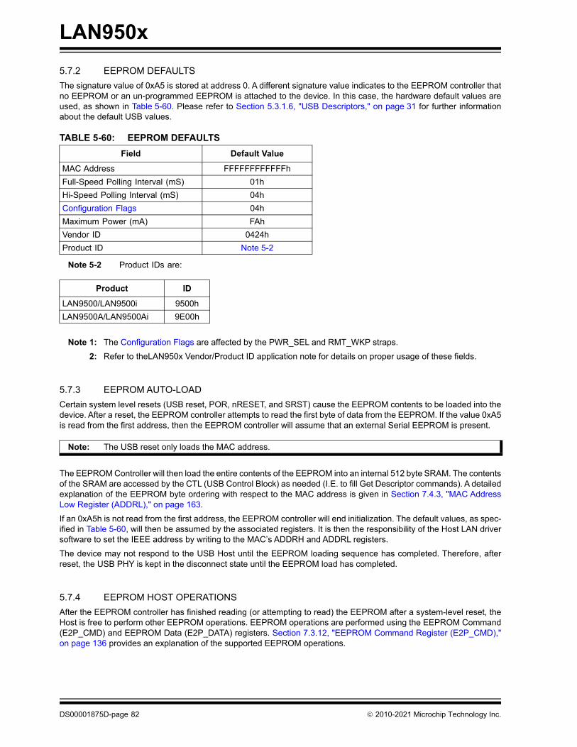
LAN950x
5.7.2 EEPROM DEFAULTS
The signature value of 0xA5 is stored at address 0. A different signature value indicates to the EEPROM controller thatno EEPROM or an un-programmed EEPROM is attached to the device. In this case, the hardware default values areused, as shown in Table 5-60. Please refer to Section 5.3.1.6, "USB Descriptors," on page 31 for further informationabout the default USB values.
Note 5-2 Product IDs are:
Note 1: The Configuration Flags are affected by the PWR_SEL and RMT_WKP straps.
2: Refer to theLAN950x Vendor/Product ID application note for details on proper usage of these fields.
5.7.3 EEPROM AUTO-LOAD
Certain system level resets (USB reset, POR, nRESET, and SRST) cause the EEPROM contents to be loaded into thedevice. After a reset, the EEPROM controller attempts to read the first byte of data from the EEPROM. If the value 0xA5is read from the first address, then the EEPROM controller will assume that an external Serial EEPROM is present.
The EEPROM Controller will then load the entire contents of the EEPROM into an internal 512 byte SRAM. The contentsof the SRAM are accessed by the CTL (USB Control Block) as needed (I.E. to fill Get Descriptor commands). A detailedexplanation of the EEPROM byte ordering with respect to the MAC address is given in Section 7.4.3, "MAC AddressLow Register (ADDRL)," on page 163.
If an 0xA5h is not read from the first address, the EEPROM controller will end initialization. The default values, as spec-ified in Table 5-60, will then be assumed by the associated registers. It is then the responsibility of the Host LAN driversoftware to set the IEEE address by writing to the MAC’s ADDRH and ADDRL registers.
The device may not respond to the USB Host until the EEPROM loading sequence has completed. Therefore, afterreset, the USB PHY is kept in the disconnect state until the EEPROM load has completed.
5.7.4 EEPROM HOST OPERATIONS
After the EEPROM controller has finished reading (or attempting to read) the EEPROM after a system-level reset, theHost is free to perform other EEPROM operations. EEPROM operations are performed using the EEPROM Command(E2P_CMD) and EEPROM Data (E2P_DATA) registers. Section 7.3.12, "EEPROM Command Register (E2P_CMD),"on page 136 provides an explanation of the supported EEPROM operations.
TABLE 5-60: EEPROM DEFAULTS
Field Default Value
MAC Address FFFFFFFFFFFFh
Full-Speed Polling Interval (mS) 01h
Hi-Speed Polling Interval (mS) 04h
Configuration Flags 04h
Maximum Power (mA) FAh
Vendor ID 0424h
Product ID Note 5-2
Product ID
LAN9500/LAN9500i 9500h
LAN9500A/LAN9500Ai 9E00h
Note: The USB reset only loads the MAC address.
DS00001875D-page 82 2010-2021 Microchip Technology Inc.
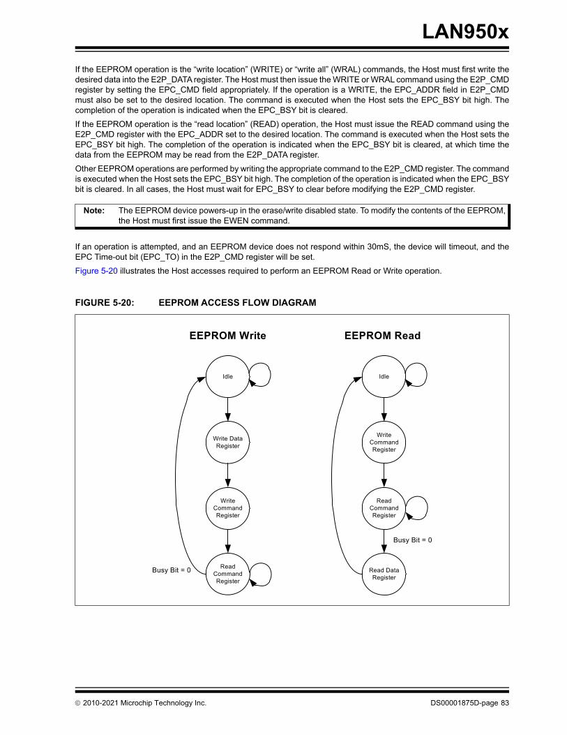
LAN950x
If the EEPROM operation is the “write location” (WRITE) or “write all” (WRAL) commands, the Host must first write thedesired data into the E2P_DATA register. The Host must then issue the WRITE or WRAL command using the E2P_CMDregister by setting the EPC_CMD field appropriately. If the operation is a WRITE, the EPC_ADDR field in E2P_CMDmust also be set to the desired location. The command is executed when the Host sets the EPC_BSY bit high. Thecompletion of the operation is indicated when the EPC_BSY bit is cleared.
If the EEPROM operation is the “read location” (READ) operation, the Host must issue the READ command using theE2P_CMD register with the EPC_ADDR set to the desired location. The command is executed when the Host sets theEPC_BSY bit high. The completion of the operation is indicated when the EPC_BSY bit is cleared, at which time thedata from the EEPROM may be read from the E2P_DATA register.
Other EEPROM operations are performed by writing the appropriate command to the E2P_CMD register. The commandis executed when the Host sets the EPC_BSY bit high. The completion of the operation is indicated when the EPC_BSYbit is cleared. In all cases, the Host must wait for EPC_BSY to clear before modifying the E2P_CMD register.
If an operation is attempted, and an EEPROM device does not respond within 30mS, the device will timeout, and theEPC Time-out bit (EPC_TO) in the E2P_CMD register will be set.
Figure 5-20 illustrates the Host accesses required to perform an EEPROM Read or Write operation.
Note: The EEPROM device powers-up in the erase/write disabled state. To modify the contents of the EEPROM,the Host must first issue the EWEN command.
FIGURE 5-20: EEPROM ACCESS FLOW DIAGRAM
Idle
Write Data Register
Write Command Register
Read Command Register
Idle
Write Command Register
Read Command Register
Read Data Register
Busy Bit = 0
Busy Bit = 0
EEPROM Write EEPROM Read
2010-2021 Microchip Technology Inc. DS00001875D-page 83
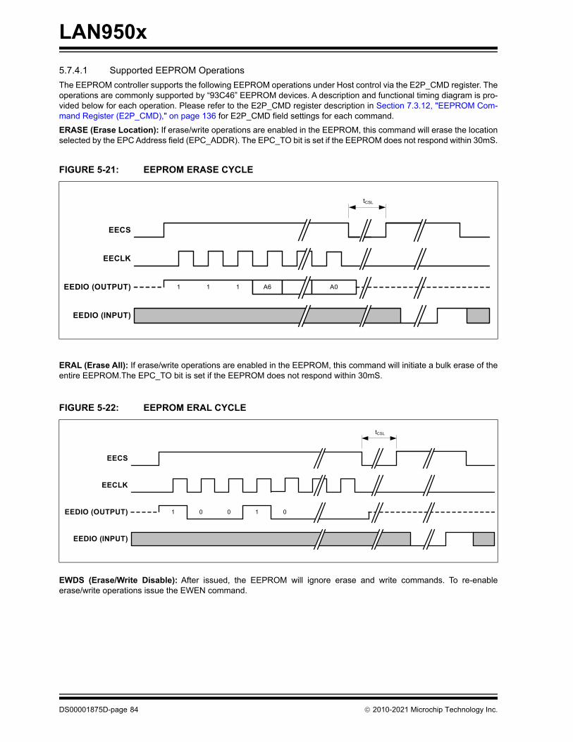
LAN950x
5.7.4.1 Supported EEPROM Operations
The EEPROM controller supports the following EEPROM operations under Host control via the E2P_CMD register. Theoperations are commonly supported by “93C46” EEPROM devices. A description and functional timing diagram is pro-vided below for each operation. Please refer to the E2P_CMD register description in Section 7.3.12, "EEPROM Com-mand Register (E2P_CMD)," on page 136 for E2P_CMD field settings for each command.
ERASE (Erase Location): If erase/write operations are enabled in the EEPROM, this command will erase the locationselected by the EPC Address field (EPC_ADDR). The EPC_TO bit is set if the EEPROM does not respond within 30mS.
ERAL (Erase All): If erase/write operations are enabled in the EEPROM, this command will initiate a bulk erase of theentire EEPROM.The EPC_TO bit is set if the EEPROM does not respond within 30mS.
EWDS (Erase/Write Disable): After issued, the EEPROM will ignore erase and write commands. To re-enableerase/write operations issue the EWEN command.
FIGURE 5-21: EEPROM ERASE CYCLE
FIGURE 5-22: EEPROM ERAL CYCLE
1
EECLK
EEDIO (INPUT)
EEDIO (OUTPUT)
EECS
1 1 A6 A0
tCSL
0
EECLK
EEDIO (INPUT)
EEDIO (OUTPUT)
EECS
1 0 1 0
tCSL
DS00001875D-page 84 2010-2021 Microchip Technology Inc.
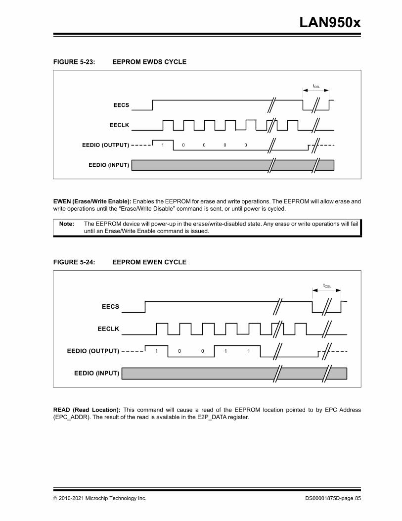
LAN950x
EWEN (Erase/Write Enable): Enables the EEPROM for erase and write operations. The EEPROM will allow erase andwrite operations until the “Erase/Write Disable” command is sent, or until power is cycled.
READ (Read Location): This command will cause a read of the EEPROM location pointed to by EPC Address(EPC_ADDR). The result of the read is available in the E2P_DATA register.
FIGURE 5-23: EEPROM EWDS CYCLE
Note: The EEPROM device will power-up in the erase/write-disabled state. Any erase or write operations will failuntil an Erase/Write Enable command is issued.
FIGURE 5-24: EEPROM EWEN CYCLE
0
EECLK
EEDIO (INPUT)
EEDIO (OUTPUT)
EECS
1 0 0 0
tCSL
0
EECLK
EEDIO (INPUT)
EEDIO (OUTPUT)
EECS
1 0 1 1
tCSL
2010-2021 Microchip Technology Inc. DS00001875D-page 85
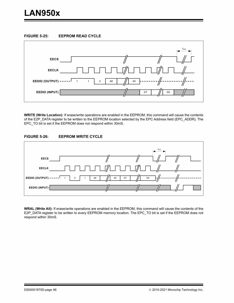
LAN950x
WRITE (Write Location): If erase/write operations are enabled in the EEPROM, this command will cause the contentsof the E2P_DATA register to be written to the EEPROM location selected by the EPC Address field (EPC_ADDR). TheEPC_TO bit is set if the EEPROM does not respond within 30mS.
WRAL (Write All): If erase/write operations are enabled in the EEPROM, this command will cause the contents of theE2P_DATA register to be written to every EEPROM memory location. The EPC_TO bit is set if the EEPROM does notrespond within 30mS.
FIGURE 5-25: EEPROM READ CYCLE
FIGURE 5-26: EEPROM WRITE CYCLE
11 0 A6
EECS
EECLK
EEDIO (OUTPUT) A0
D7 D0EEDIO (INPUT)
tCSL
0
EECLK
EEDIO (INPUT)
EEDIO (OUTPUT)
EECS
1 1 A6 A0 D7 D0
tCSL
DS00001875D-page 86 2010-2021 Microchip Technology Inc.
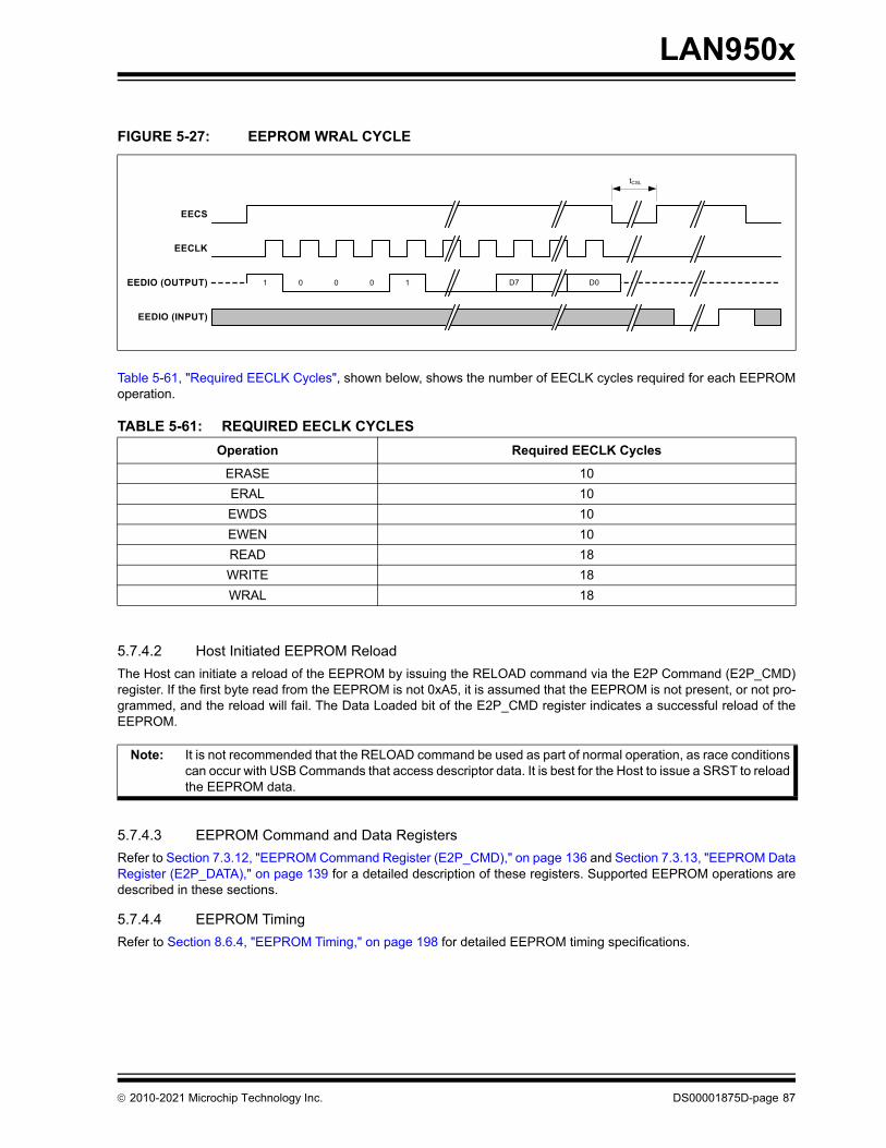
LAN950x
Table 5-61, "Required EECLK Cycles", shown below, shows the number of EECLK cycles required for each EEPROMoperation.
5.7.4.2 Host Initiated EEPROM Reload
The Host can initiate a reload of the EEPROM by issuing the RELOAD command via the E2P Command (E2P_CMD)register. If the first byte read from the EEPROM is not 0xA5, it is assumed that the EEPROM is not present, or not pro-grammed, and the reload will fail. The Data Loaded bit of the E2P_CMD register indicates a successful reload of theEEPROM.
5.7.4.3 EEPROM Command and Data Registers
Refer to Section 7.3.12, "EEPROM Command Register (E2P_CMD)," on page 136 and Section 7.3.13, "EEPROM DataRegister (E2P_DATA)," on page 139 for a detailed description of these registers. Supported EEPROM operations aredescribed in these sections.
5.7.4.4 EEPROM Timing
Refer to Section 8.6.4, "EEPROM Timing," on page 198 for detailed EEPROM timing specifications.
FIGURE 5-27: EEPROM WRAL CYCLE
TABLE 5-61: REQUIRED EECLK CYCLES
Operation Required EECLK Cycles
ERASE 10
ERAL 10
EWDS 10
EWEN 10
READ 18
WRITE 18
WRAL 18
Note: It is not recommended that the RELOAD command be used as part of normal operation, as race conditionscan occur with USB Commands that access descriptor data. It is best for the Host to issue a SRST to reloadthe EEPROM data.
0
EECLK
EEDIO (INPUT)
EEDIO (OUTPUT)
EECS
1 D7 D00 0 1
tCSL
2010-2021 Microchip Technology Inc. DS00001875D-page 87
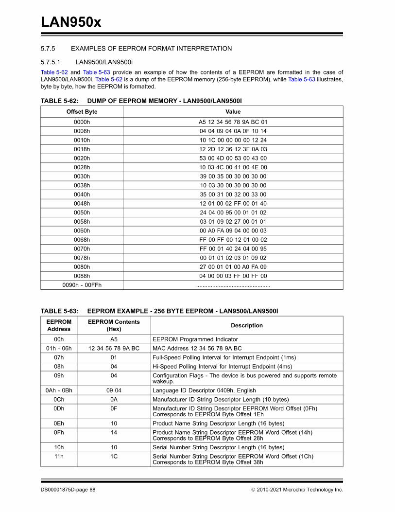
LAN950x
5.7.5 EXAMPLES OF EEPROM FORMAT INTERPRETATION
5.7.5.1 LAN9500/LAN9500i
Table 5-62 and Table 5-63 provide an example of how the contents of a EEPROM are formatted in the case ofLAN9500/LAN9500i. Table 5-62 is a dump of the EEPROM memory (256-byte EEPROM), while Table 5-63 illustrates,byte by byte, how the EEPROM is formatted.
TABLE 5-62: DUMP OF EEPROM MEMORY - LAN9500/LAN9500I
Offset Byte Value
0000h A5 12 34 56 78 9A BC 01
0008h 04 04 09 04 0A 0F 10 14
0010h 10 1C 00 00 00 00 12 24
0018h 12 2D 12 36 12 3F 0A 03
0020h 53 00 4D 00 53 00 43 00
0028h 10 03 4C 00 41 00 4E 00
0030h 39 00 35 00 30 00 30 00
0038h 10 03 30 00 30 00 30 00
0040h 35 00 31 00 32 00 33 00
0048h 12 01 00 02 FF 00 01 40
0050h 24 04 00 95 00 01 01 02
0058h 03 01 09 02 27 00 01 01
0060h 00 A0 FA 09 04 00 00 03
0068h FF 00 FF 00 12 01 00 02
0070h FF 00 01 40 24 04 00 95
0078h 00 01 01 02 03 01 09 02
0080h 27 00 01 01 00 A0 FA 09
0088h 04 00 00 03 FF 00 FF 00
0090h - 00FFh ..............................................
TABLE 5-63: EEPROM EXAMPLE - 256 BYTE EEPROM - LAN9500/LAN9500I
EEPROMAddress
EEPROM Contents(Hex)
Description
00h A5 EEPROM Programmed Indicator
01h - 06h 12 34 56 78 9A BC MAC Address 12 34 56 78 9A BC
07h 01 Full-Speed Polling Interval for Interrupt Endpoint (1ms)
08h 04 Hi-Speed Polling Interval for Interrupt Endpoint (4ms)
09h 04 Configuration Flags - The device is bus powered and supports remote wakeup.
0Ah - 0Bh 09 04 Language ID Descriptor 0409h, English
0Ch 0A Manufacturer ID String Descriptor Length (10 bytes)
0Dh 0F Manufacturer ID String Descriptor EEPROM Word Offset (0Fh)Corresponds to EEPROM Byte Offset 1Eh
0Eh 10 Product Name String Descriptor Length (16 bytes)
0Fh 14 Product Name String Descriptor EEPROM Word Offset (14h)Corresponds to EEPROM Byte Offset 28h
10h 10 Serial Number String Descriptor Length (16 bytes)
11h 1C Serial Number String Descriptor EEPROM Word Offset (1Ch)Corresponds to EEPROM Byte Offset 38h
DS00001875D-page 88 2010-2021 Microchip Technology Inc.
LAN950x
12h 00 Configuration String Descriptor Length (0 bytes - NA)
13h 00 Configuration String Descriptor Word Offset (Don’t Care)
14h 00 Interface String Descriptor Length (0 bytes - NA)
15h 00 Interface String Descriptor Word Offset (Don’t Care)
16h 12 Hi-Speed Device Descriptor Length (18 bytes)
17h 24 Hi-Speed Device Descriptor Word Offset (24h)Corresponds to EEPROM Byte Offset 48h
18h 12 Hi-Speed Configuration and Interface Descriptor Length (18 bytes)
19h 2D Hi-Speed Configuration and Interface Descriptor Word Offset (2Dh)Corresponds to EEPROM Byte Offset 5Ah
1Ah 12 Full-Speed Device Descriptor Length (18 bytes)
1Bh 36 Full-Speed Device Descriptor Word Offset (36h)Corresponds to EEPROM Byte Offset 6Ch
1Ch 12 Full-Speed Configuration and Interface Descriptor Length (18bytes)
1Dh 3F Full-Speed Configuration and Interface Descriptor Word Offset (3Fh)Corresponds to EEPROM Byte Offset 7Eh
1Eh 0A Size of Manufacturer ID String Descriptor (10 bytes)
1Fh 03 Descriptor Type (String Descriptor - 03h)
20h-27h 53 00 4D 00 53 00 43 00 Manufacturer ID String (“MCHP” in UNICODE)
28h 10 Size of Product Name String Descriptor (16 bytes)
29h 03 Descriptor Type (String Descriptor - 03h)
2Ah-37h 4C 00 41 00 4E 00 39 00 35 00 30 00 30 00
Product Name String (“LAN9500” in UNICODE)
38h 10 Size of Serial Number String Descriptor (16 bytes)
39h 03 Descriptor Type (String Descriptor - 03h)
3Ah-47h 30 00 30 00 30 00 35 00 31 00 32 00 33 00
Serial Number String (“0005123” in UNICODE)
48h 12 Size of Hi-Speed Device Descriptor in Bytes (18 bytes)
49h 01 Descriptor Type (Device Descriptor - 01h)
4Ah-4Bh 00 02 USB Specification Number that the device complies with (0200h)
4Ch FF Class Code
4Dh 00 Subclass Code
4Eh 01 Protocol Code
4Fh 40 Maximum Packet Size for Endpoint 0
50h-51h 24 04 Vendor ID (0424h)
52h-53h 00 95 Product ID (9500h)
54h-55h 00 01 Device Release Number (0100h)
56h 01 Index of Manufacturer String Descriptor
57h 02 Index of Product String Descriptor
58h 03 Index of Serial Number String Descriptor
59h 01 Number of Possible Configurations
5Ah 09 Size of Hi-Speed Configuration Descriptor in bytes (9 bytes)
5Bh 02 Descriptor Type (Configuration Descriptor - 02h)
5Ch-5Dh 27 00 Total length in bytes of data returned (0027h = 39 bytes)
5Eh 01 Number of Interfaces
5Fh 01 Value to use as an argument to select this configuration
TABLE 5-63: EEPROM EXAMPLE - 256 BYTE EEPROM - LAN9500/LAN9500I (CONTINUED)
EEPROMAddress
EEPROM Contents(Hex)
Description
2010-2021 Microchip Technology Inc. DS00001875D-page 89
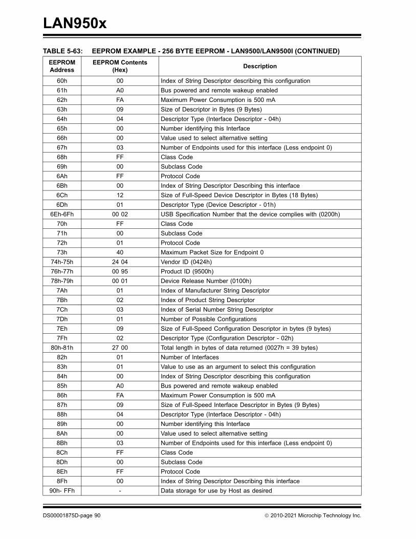
LAN950x
60h 00 Index of String Descriptor describing this configuration
61h A0 Bus powered and remote wakeup enabled
62h FA Maximum Power Consumption is 500 mA
63h 09 Size of Descriptor in Bytes (9 Bytes)
64h 04 Descriptor Type (Interface Descriptor - 04h)
65h 00 Number identifying this Interface
66h 00 Value used to select alternative setting
67h 03 Number of Endpoints used for this interface (Less endpoint 0)
68h FF Class Code
69h 00 Subclass Code
6Ah FF Protocol Code
6Bh 00 Index of String Descriptor Describing this interface
6Ch 12 Size of Full-Speed Device Descriptor in Bytes (18 Bytes)
6Dh 01 Descriptor Type (Device Descriptor - 01h)
6Eh-6Fh 00 02 USB Specification Number that the device complies with (0200h)
70h FF Class Code
71h 00 Subclass Code
72h 01 Protocol Code
73h 40 Maximum Packet Size for Endpoint 0
74h-75h 24 04 Vendor ID (0424h)
76h-77h 00 95 Product ID (9500h)
78h-79h 00 01 Device Release Number (0100h)
7Ah 01 Index of Manufacturer String Descriptor
7Bh 02 Index of Product String Descriptor
7Ch 03 Index of Serial Number String Descriptor
7Dh 01 Number of Possible Configurations
7Eh 09 Size of Full-Speed Configuration Descriptor in bytes (9 bytes)
7Fh 02 Descriptor Type (Configuration Descriptor - 02h)
80h-81h 27 00 Total length in bytes of data returned (0027h = 39 bytes)
82h 01 Number of Interfaces
83h 01 Value to use as an argument to select this configuration
84h 00 Index of String Descriptor describing this configuration
85h A0 Bus powered and remote wakeup enabled
86h FA Maximum Power Consumption is 500 mA
87h 09 Size of Full-Speed Interface Descriptor in Bytes (9 Bytes)
88h 04 Descriptor Type (Interface Descriptor - 04h)
89h 00 Number identifying this Interface
8Ah 00 Value used to select alternative setting
8Bh 03 Number of Endpoints used for this interface (Less endpoint 0)
8Ch FF Class Code
8Dh 00 Subclass Code
8Eh FF Protocol Code
8Fh 00 Index of String Descriptor Describing this interface
90h- FFh - Data storage for use by Host as desired
TABLE 5-63: EEPROM EXAMPLE - 256 BYTE EEPROM - LAN9500/LAN9500I (CONTINUED)
EEPROMAddress
EEPROM Contents(Hex)
Description
DS00001875D-page 90 2010-2021 Microchip Technology Inc.
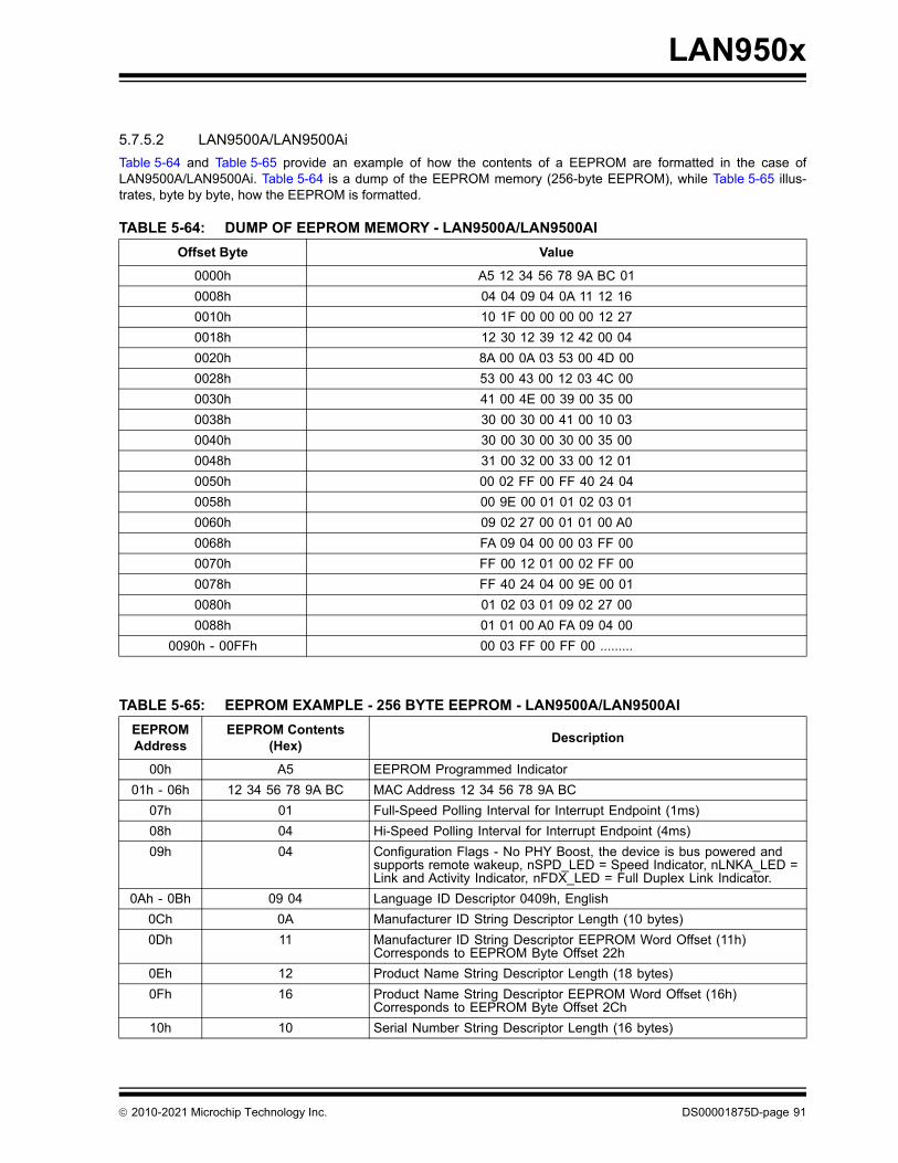
LAN950x
5.7.5.2 LAN9500A/LAN9500Ai
Table 5-64 and Table 5-65 provide an example of how the contents of a EEPROM are formatted in the case ofLAN9500A/LAN9500Ai. Table 5-64 is a dump of the EEPROM memory (256-byte EEPROM), while Table 5-65 illus-trates, byte by byte, how the EEPROM is formatted.
TABLE 5-64: DUMP OF EEPROM MEMORY - LAN9500A/LAN9500AI
Offset Byte Value
0000h A5 12 34 56 78 9A BC 01
0008h 04 04 09 04 0A 11 12 16
0010h 10 1F 00 00 00 00 12 27
0018h 12 30 12 39 12 42 00 04
0020h 8A 00 0A 03 53 00 4D 00
0028h 53 00 43 00 12 03 4C 00
0030h 41 00 4E 00 39 00 35 00
0038h 30 00 30 00 41 00 10 03
0040h 30 00 30 00 30 00 35 00
0048h 31 00 32 00 33 00 12 01
0050h 00 02 FF 00 FF 40 24 04
0058h 00 9E 00 01 01 02 03 01
0060h 09 02 27 00 01 01 00 A0
0068h FA 09 04 00 00 03 FF 00
0070h FF 00 12 01 00 02 FF 00
0078h FF 40 24 04 00 9E 00 01
0080h 01 02 03 01 09 02 27 00
0088h 01 01 00 A0 FA 09 04 00
0090h - 00FFh 00 03 FF 00 FF 00 .........
TABLE 5-65: EEPROM EXAMPLE - 256 BYTE EEPROM - LAN9500A/LAN9500AI
EEPROMAddress
EEPROM Contents(Hex)
Description
00h A5 EEPROM Programmed Indicator
01h - 06h 12 34 56 78 9A BC MAC Address 12 34 56 78 9A BC
07h 01 Full-Speed Polling Interval for Interrupt Endpoint (1ms)
08h 04 Hi-Speed Polling Interval for Interrupt Endpoint (4ms)
09h 04 Configuration Flags - No PHY Boost, the device is bus powered and supports remote wakeup, nSPD_LED = Speed Indicator, nLNKA_LED = Link and Activity Indicator, nFDX_LED = Full Duplex Link Indicator.
0Ah - 0Bh 09 04 Language ID Descriptor 0409h, English
0Ch 0A Manufacturer ID String Descriptor Length (10 bytes)
0Dh 11 Manufacturer ID String Descriptor EEPROM Word Offset (11h)Corresponds to EEPROM Byte Offset 22h
0Eh 12 Product Name String Descriptor Length (18 bytes)
0Fh 16 Product Name String Descriptor EEPROM Word Offset (16h)Corresponds to EEPROM Byte Offset 2Ch
10h 10 Serial Number String Descriptor Length (16 bytes)
2010-2021 Microchip Technology Inc. DS00001875D-page 91
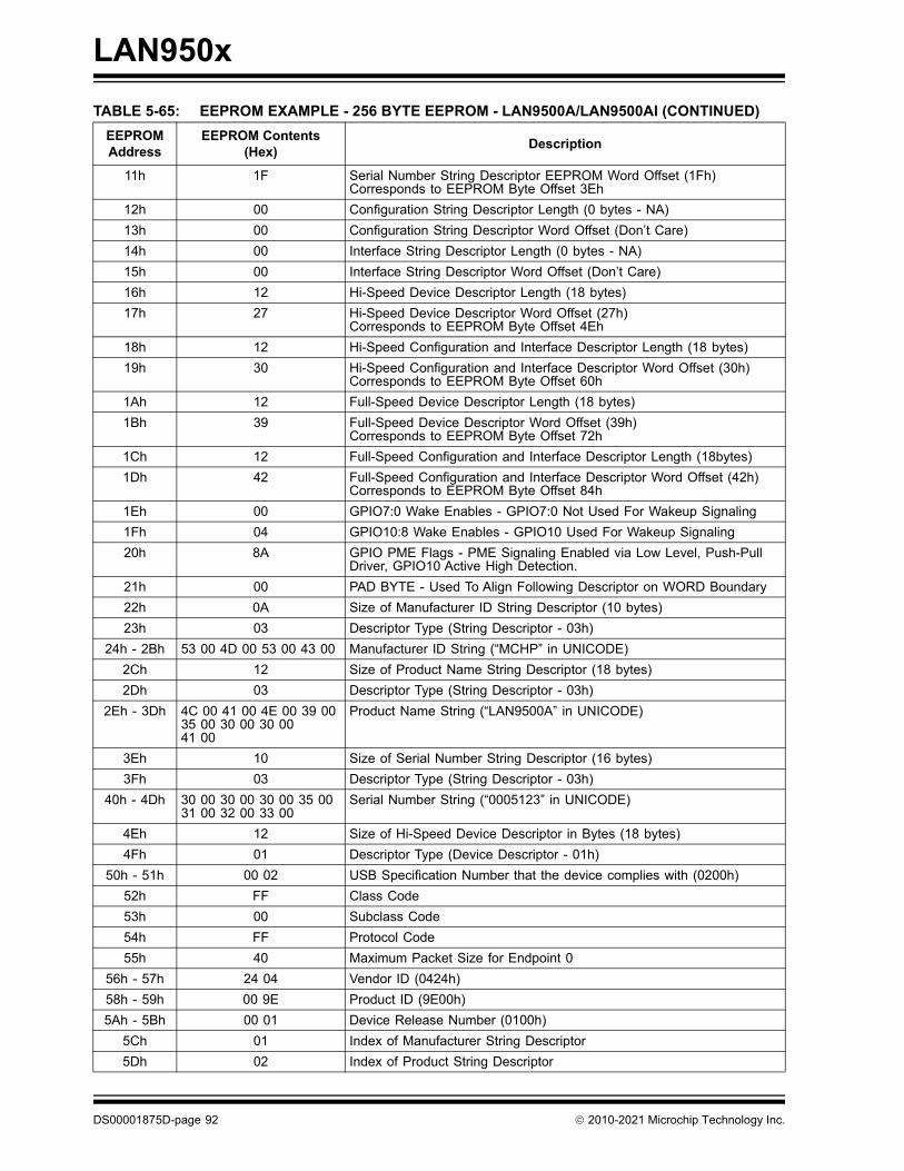
LAN950x
11h 1F Serial Number String Descriptor EEPROM Word Offset (1Fh)Corresponds to EEPROM Byte Offset 3Eh
12h 00 Configuration String Descriptor Length (0 bytes - NA)
13h 00 Configuration String Descriptor Word Offset (Don’t Care)
14h 00 Interface String Descriptor Length (0 bytes - NA)
15h 00 Interface String Descriptor Word Offset (Don’t Care)
16h 12 Hi-Speed Device Descriptor Length (18 bytes)
17h 27 Hi-Speed Device Descriptor Word Offset (27h)Corresponds to EEPROM Byte Offset 4Eh
18h 12 Hi-Speed Configuration and Interface Descriptor Length (18 bytes)
19h 30 Hi-Speed Configuration and Interface Descriptor Word Offset (30h)Corresponds to EEPROM Byte Offset 60h
1Ah 12 Full-Speed Device Descriptor Length (18 bytes)
1Bh 39 Full-Speed Device Descriptor Word Offset (39h)Corresponds to EEPROM Byte Offset 72h
1Ch 12 Full-Speed Configuration and Interface Descriptor Length (18bytes)
1Dh 42 Full-Speed Configuration and Interface Descriptor Word Offset (42h)Corresponds to EEPROM Byte Offset 84h
1Eh 00 GPIO7:0 Wake Enables - GPIO7:0 Not Used For Wakeup Signaling
1Fh 04 GPIO10:8 Wake Enables - GPIO10 Used For Wakeup Signaling
20h 8A GPIO PME Flags - PME Signaling Enabled via Low Level, Push-Pull Driver, GPIO10 Active High Detection.
21h 00 PAD BYTE - Used To Align Following Descriptor on WORD Boundary
22h 0A Size of Manufacturer ID String Descriptor (10 bytes)
23h 03 Descriptor Type (String Descriptor - 03h)
24h - 2Bh 53 00 4D 00 53 00 43 00 Manufacturer ID String (“MCHP” in UNICODE)
2Ch 12 Size of Product Name String Descriptor (18 bytes)
2Dh 03 Descriptor Type (String Descriptor - 03h)
2Eh - 3Dh 4C 00 41 00 4E 00 39 00 35 00 30 00 30 0041 00
Product Name String (“LAN9500A” in UNICODE)
3Eh 10 Size of Serial Number String Descriptor (16 bytes)
3Fh 03 Descriptor Type (String Descriptor - 03h)
40h - 4Dh 30 00 30 00 30 00 35 00 31 00 32 00 33 00
Serial Number String (“0005123” in UNICODE)
4Eh 12 Size of Hi-Speed Device Descriptor in Bytes (18 bytes)
4Fh 01 Descriptor Type (Device Descriptor - 01h)
50h - 51h 00 02 USB Specification Number that the device complies with (0200h)
52h FF Class Code
53h 00 Subclass Code
54h FF Protocol Code
55h 40 Maximum Packet Size for Endpoint 0
56h - 57h 24 04 Vendor ID (0424h)
58h - 59h 00 9E Product ID (9E00h)
5Ah - 5Bh 00 01 Device Release Number (0100h)
5Ch 01 Index of Manufacturer String Descriptor
5Dh 02 Index of Product String Descriptor
TABLE 5-65: EEPROM EXAMPLE - 256 BYTE EEPROM - LAN9500A/LAN9500AI (CONTINUED)
EEPROMAddress
EEPROM Contents(Hex)
Description
DS00001875D-page 92 2010-2021 Microchip Technology Inc.
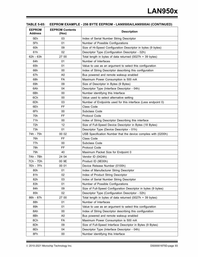
LAN950x
5Eh 03 Index of Serial Number String Descriptor
5Fh 01 Number of Possible Configurations
60h 09 Size of Hi-Speed Configuration Descriptor in bytes (9 bytes)
61h 02 Descriptor Type (Configuration Descriptor - 02h)
62h - 63h 27 00 Total length in bytes of data returned (0027h = 39 bytes)
64h 01 Number of Interfaces
65h 01 Value to use as an argument to select this configuration
66h 00 Index of String Descriptor describing this configuration
67h A0 Bus powered and remote wakeup enabled
68h FA Maximum Power Consumption is 500 mA
69h 09 Size of Descriptor in Bytes (9 Bytes)
6Ah 04 Descriptor Type (Interface Descriptor - 04h)
6Bh 00 Number identifying this Interface
6Ch 00 Value used to select alternative setting
6Dh 03 Number of Endpoints used for this interface (Less endpoint 0)
6Eh FF Class Code
6Fh 00 Subclass Code
70h FF Protocol Code
71h 00 Index of String Descriptor Describing this interface
72h 12 Size of Full-Speed Device Descriptor in Bytes (18 Bytes)
73h 01 Descriptor Type (Device Descriptor - 01h)
74h - 75h 00 02 USB Specification Number that the device complies with (0200h)
76h FF Class Code
77h 00 Subclass Code
78h FF Protocol Code
79h 40 Maximum Packet Size for Endpoint 0
7Ah - 7Bh 24 04 Vendor ID (0424h)
7Ch - 7Dh 00 9E Product ID (9E00h)
7Eh - 7Fh 00 01 Device Release Number (0100h)
80h 01 Index of Manufacturer String Descriptor
81h 02 Index of Product String Descriptor
82h 03 Index of Serial Number String Descriptor
83h 01 Number of Possible Configurations
84h 09 Size of Full-Speed Configuration Descriptor in bytes (9 bytes)
85h 02 Descriptor Type (Configuration Descriptor - 02h)
86h - 87h 27 00 Total length in bytes of data returned (0027h = 39 bytes)
88h 01 Number of Interfaces
89h 01 Value to use as an argument to select this configuration
8Ah 00 Index of String Descriptor describing this configuration
8Bh A0 Bus powered and remote wakeup enabled
8Ch FA Maximum Power Consumption is 500 mA
8Dh 09 Size of Full-Speed Interface Descriptor in Bytes (9 Bytes)
8Eh 04 Descriptor Type (Interface Descriptor - 04h)
8Fh 00 Number identifying this Interface
TABLE 5-65: EEPROM EXAMPLE - 256 BYTE EEPROM - LAN9500A/LAN9500AI (CONTINUED)
EEPROMAddress
EEPROM Contents(Hex)
Description
2010-2021 Microchip Technology Inc. DS00001875D-page 93
LAN950x
5.8 Customized Operation Without EEPROM
Customized operation without EEPROM is supported only by LAN9500A/LAN9500Ai.
The device provides the capability to customize operation without the use of an EEPROM. Descriptor information andinitialization quantities normally fetched from EEPROM and used to initialize descriptors and elements of the SystemControl and Status Registers may be specified via an alternate mechanism. This alternate mechanism involves the useof the Descriptor RAM in conjunction with the Attribute Registers and select elements of the System Control and StatusRegisters. The software device driver orchestrates the process by performing the following actions in the order indi-cated:
• Initialization of SCSR Elements in Lieu of EEPROM Load
• Attribute Register Initialization
• Descriptor RAM Initialization
• Enable Descriptor RAM and Flag Attribute Registers as Source
• Inhibit Reset of Select SCSR Elements
The following subsections explain these actions. The attribute registers must be written prior to initializing the DescriptorRAM. Failure to do this will prevent the PWR_SEL and RMT_WKUP flags from being overwritten by the bmAttributesof the Configuration Descriptor.
5.8.1 INITIALIZATION OF SCSR ELEMENTS IN LIEU OF EEPROM LOAD
During EEPROM operation, the following register fields are initialized by the hardware using the values contained in theEEPROM. In the absence of an EEPROM, the software device driver must initialize these quantities:
• MAC Address High Register (ADDRH) and MAC Address Low Register (ADDRL)
• PHY Boost (PHY_BOOST) field of Hardware Configuration Register (HW_CFG)
• LED Select (LED_SEL) bit of the LED General Purpose IO Configuration Register (LED_GPIO_CFG)
• GPIO Wake 0-10 (GPIOWKn) field of the General Purpose IO Wake Enable and Polarity Register (GPIO_WAKE)
5.8.2 ATTRIBUTE REGISTER INITIALIZATION
The Attribute Registers are as follows:
• HS Descriptor Attributes Register (HS_ATTR)
• FS Descriptor Attributes Register (FS_ATTR)
• String Descriptor Attributes Register 0 (STRNG_ATTR0)
• String Descriptor Attributes Register 1 (STRNG_ATTR1)
• Flag Attributes Register (FLAG_ATTR)
All of these registers, with the exception of FLAG_ATTR, contain fields defining the lengths of the descriptors writteninto the Descriptor RAM. If the descriptor is not written into the Descriptor RAM, the associated entry in the AttributesRegister must be written as 0. Writing an erroneous or illegal length will result in untoward operation and unexpectedresults.
90h 00 Value used to select alternative setting
91h 03 Number of Endpoints used for this interface (Less endpoint 0)
92h FF Class Code
93h 00 Subclass Code
94h FF Protocol Code
95h 00 Index of String Descriptor Describing this interface
96h - FFh - Data storage for use by Host as desired
TABLE 5-65: EEPROM EXAMPLE - 256 BYTE EEPROM - LAN9500A/LAN9500AI (CONTINUED)
EEPROMAddress
EEPROM Contents(Hex)
Description
DS00001875D-page 94 2010-2021 Microchip Technology Inc.
LAN950x
The Flag Attributes Register (FLAG_ATTR) provides the mechanism to initialize components of the Configuration Flagsand GPIO PME Flags that are stand-alone and not part of any other System Control and Status Register. DuringEEPROM operation, the analogous fields in this register are read by the hardware from the EEPROM and are not avail-able to the software for read-back or modification.
Note 1: The software device driver must initialize these registers prior to initializing the Descriptor RAM.
2: The bmAttributes field of the HS and FS descriptors in descriptor RAM (if present) must be consistent withthe contents of the Flag Attributes Register (FLAG_ATTR).
5.8.3 DESCRIPTOR RAM INITIALIZATION
The Descriptor RAM contents are initialized using the Data Port registers. The Data Port registers are used to select theDescriptor RAM and write the descriptor elements into it. The Descriptor RAM is 512 bytes in length. Every descriptorwritten into the Descriptor RAM must be DWORD aligned. The Attribute Registers discussed in Section 5.8.2 must bewritten with the length of the descriptors written into the Descriptor RAM. If a descriptor is not used, hence not writteninto Descriptor RAM, its length must be written as 0 into the associated Attribute Register.
Note 1: The Attribute Registers must be initialized before the Descriptor RAM.
2: Address 0 of the Descriptor RAM is always reserved for the Language ID descriptor, even if it will not besupported.
The descriptors must be written in the following order, starting at address 0 of the RAM and observing the DWORD align-ment rule:
• Language ID Descriptor
• Manufacturing String Descriptor (String Index 1)
• Product Name String Descriptor (String Index 2)
• Serial Number String Descriptor (String Index 3)
• Configuration String Descriptor (String Index 4)
• Interface String Descriptor (String Index 5)
• HS Device Descriptor
• HS Configuration Descriptor
• FS Device Descriptor
• FS Configuration Descriptor
An example of Descriptor RAM use is illustrated in Figure 5-28.
As in the case of descriptors specified in EEPROM, the following restrictions apply to descriptors written into DescriptorRAM:
1. For Device Descriptors, the only valid values for the length are 0 and 18. The descriptor size for the DeviceDescriptors specified in the Descriptor RAM is a don't care and always overwritten by HW to 0x12 when trans-mitting the descriptor to the host.
2. The descriptor type for Device Descriptors specified in the Descriptor RAM is a don't care and is always overwrit-ten by HW to 0x1 when transmitting the descriptor to the host.
3. For the Configuration and Interface descriptor, the only valid values for the length are 0 and 18. The descriptorsize for the Device Descriptors specified in the Descriptor RAM is a don't care and always overwritten by HW to0x12 when transmitting the descriptor to the host.
4. The descriptor type for the configuration descriptors specified in the Descriptor RAM is a don't care and alwaysoverwritten by HW to 0x2 when transmitting the descriptor to the host.
5. If a string descriptor does not exist in the Descriptor RAM, the referencing descriptor must contain 00h for therespective string index field.
6. If all string descriptor lengths are zero than a Language ID will not be supported.
Note 1: The first entry in the Descriptor RAM is always reserved for the Language ID descriptor, even if it will not besupported.
2: Descriptors specified having bcdUSB, bMaxPacketSize0, and bNumConfigurations fields defined with val-ues other than 0200h, 40h, and 1, respectively, will result in unwanted behavior and untoward results.
The RAM Test Mode Enable (TESTEN) bit must be deasserted after programming the descriptor RAM.
2010-2021 Microchip Technology Inc. DS00001875D-page 95
LAN950x
5.8.4 ENABLE DESCRIPTOR RAM AND FLAG ATTRIBUTE REGISTERS AS SOURCE
The EEPROM Emulation Enable (EEM) bit of the Hardware Configuration Register (HW_CFG) must be configured bythe software device driver to use the Descriptor RAM and the Attribute Registers for custom operation. Upon assertionof EEPROM Emulation Enable (EEM), the hardware will utilize the Descriptor information contained in the DescriptorRAM, the Attributes Registers, and the values of the items listed in Section 5.8.1 to facilitate custom operation.
5.8.5 INHIBIT RESET OF SELECT SCSR ELEMENTS
The software device driver must take care to ensure that the contents of the Descriptor RAM and SCSR register contentcritical to custom operation using Descriptor RAM are preserved across reset operations other than POR. The drivermust configure the Reset Protection (RST_PROTECT) bit of the Hardware Configuration Register (HW_CFG) in orderto accomplish this.
The following registers have contents that can be preserved across all resets other than POR. Consult the register’sdescription for additional details.
• Descriptor RAM
• Attribute Registers
FIGURE 5-28: DESCRIPTOR RAM EXAMPLE
Language ID DescriptorManufacturing String Descriptor
Product Name String Descriptor
Serial Number String Descriptor
Configuration String DescriptorInterface String Descriptor
HS Device Descriptor
HS Configuration and Interface Descriptor
FS Device Descriptor
FS Configuration and Interface Descriptor
0123456789
0A0B0C0D0E0F101112131415161718191A1B1C1D1E
DATAPORT ADDR
= Unused Space Required For Alignment Purposes
DS00001875D-page 96 2010-2021 Microchip Technology Inc.
LAN950x
• MAC Address High Register (ADDRH) and MAC Address Low Register (ADDRL)
• Hardware Configuration Register (HW_CFG)
• LED General Purpose IO Configuration Register (LED_GPIO_CFG)
• General Purpose IO Wake Enable and Polarity Register (GPIO_WAKE)
5.9 Device Clocking
The device requires a fixed-frequency 25MHz clock source. This is typically provided by attaching a 25MHz crystal tothe XI and XO pins. The clock can optionally be provided by driving the XI input pin with a single-ended 25MHz clocksource. If a single-ended source is selected, the clock input must run continuously for normal device operation.
Internally, the device generates its required clocks with a phase-locked loop (PLL). It reduces its power consumption inseveral of its operating states by disabling its internal PLL and derivative clocks. The 25MHz clock remains operationalin all states where power is applied.
5.10 Device Power Sources
The device may be soft powered by the USB bus or self powered via external power supplies. The following external3.3V power supplies are required when power is not being furnished by the USB bus:
• VDD33IO, VDD33A
5.11 Power States
The following power states are featured.
• UNPOWERED
• NORMAL (Unconfigured and Configured)
• Suspend (SUSPEND0, SUSPEND1, SUSPEND2, and SUSPEND3)
All four SUSPEND states are supported by LAN9500A/LAN9500Ai. SUSPEND3 is not supported byLAN9500/LAN9500i.
Figure 5-29 illustrates the power states and allowed state transitions.
Note: The device also uses power supplied by an internal regulator and connection does not vary. Since the reg-ulated supply is derived from VDD33IO, there is no need to discuss it separately.
FIGURE 5-29: POWER STATES
UN PO W ER ED
N O R M AL (C onfigured )
SU SPEND 0 SUSPEND 1 SUSPEND 2
USB Resum e || W O L || G PIO
USB Suspend
USB Resum e || G PIO
USB Suspend
USB Resum e || Energy Detect ||
G PIO
USB Suspend
!VBUS_DET(Any state)
(PO R || nRESET || USB Reset || SRST) && VBUS_DET
N O R M AL (Unconfigured )
C onfiguredDeconfigured
USB Resum e || G PIO
USB Suspend
SUSPEND 3
USB SuspendUSB Resum e ||
Fram e Received || G PIO
VBUS_DETAsserted
2010-2021 Microchip Technology Inc. DS00001875D-page 97
LAN950x
Note 1: It is not possible to transition from SUSPEND2 to NORMAL Configured if SUSPEND2 was entered via atransition from NORMAL Unconfigured.
2: When the device is bus powered, VBUS_DET is tied to 1b. Therefore, the UNPOWERED state only hasmeaning for self powered operation.
5.11.1 UNPOWERED STATE
The UNPOWERED state provides a mechanism for the device to conserve power when VBUS_DET is not connectedand the device is self powered.
The device may initially enter the UNPOWERED state when a POR occurs and USB power is not detected. This statepersists until the VBUS_DET is asserted. The UNPOWERED state is alternatively entered whenever VBUS_DET deas-serts.
In order to make the LAN950x fully operational, the Host must configure the device, which places it in the NORMALConfigured state.
5.11.2 NORMAL STATE
The NORMAL state is the fully functional state of the device. The are two flavors of the NORMAL state, NORMAL Con-figured and NORMAL Unconfigured. In the Configured variation, all chip subsystem modules are enabled. The Uncon-figured variation has only a subset of the modules enabled. The reduced functionality allows for power savings.
This NORMAL state is entered by any of the following methods.
• A system reset and VBUS_DET is asserted.
• The device is in the UNPOWERED state and VBUS_DET is asserted.
• The device is suspended and the Host issues resume signaling.
• The device is suspended and a wake event is detected.
5.11.2.1 Unconfigured
Upon initially entering the NORMAL state, the device is unconfigured. The device transitions to the NORMAL Configuredstate upon the Host completion of the USB configuration.
It is possible for the device to be deconfigured by the Host after being placed in the NORMAL configured state, via aset_configuration command. In this case, the CPM must place the device back into the NORMAL Unconfigured state.
5.11.2.2 Reset Operation
After a system reset, the device is placed into the NORMAL Unconfigured state. When in the NORMAL state, theREADY bit in the Power Management Control Register (PMT_CTL) is set. This READY bit is useful to the Host after aUSB reset occurs. In this case, it indicates that the values in the EEPROM have been completely loaded.
5.11.2.3 Suspend Operation
When returning to the NORMAL state from the SUSPEND state, the USB context is maintained. After entering the NOR-MAL state, the READY bit in the PMT_CTL register is asserted.
5.11.3 SUSPEND STATES
The SUSPEND state is entered after the USB Host suspends the device. The LAN950x family features four (Note 5-3)variations of the USB SUSPEND state. Each state offers different options in terms of power consumption and wakeupsupport.
A SUSPEND state is entered via a transition from the NORMAL state. The SUSPEND_MODE field in the Power Man-agement Control Register (PMT_CTL), indicates which SUSPEND state is to be used. The Host sets the value of thisfield to select the desired suspend state, then sends suspend signaling. A transfer back to the NORMAL state occurswhen the Host sends resume signaling or a wakeup event is detected.
The device can be suspended from the NORMAL Unconfigured state. In this scenario, it is only possible to transition tothe SUSPEND2 state. Subsequent resume signaling or a wakeup event will cause the device to transition back to theNORMAL Unconfigured state.
Note: If the originating suspend state is SUSPEND2, the Host is required to reinitialize the Ethernet PHY regis-ters.
DS00001875D-page 98 2010-2021 Microchip Technology Inc.
LAN950x
Note 5-3 All four SUSPEND states are supported by LAN9500A/LAN9500Ai. SUSPEND3 is not supported byLAN9500/LAN9500i.
5.11.3.1 Reset from Suspend
All suspend states must respond to a USB Reset and pin reset, nRESET. The application of these resets result in thedevice’s hardware being re-initialized and placed into the NORMAL Unconfigured state.
5.11.3.2 SUSPEND0
This state is entered from the NORMAL state when the device is suspended and the SUSPEND_MODE field in thePower Management Control Register (PMT_CTL) is set to 00b.
Refer to Section 5.12.2.1, "Enabling GPIO Wake Events," on page 106, Section 5.12.2.2, "Enabling WOL Wake Events,"on page 107, and Section 5.12.2.4, "Enabling PHY Link Up Wake Events (LAN9500A/LAN9500Ai ONLY)," on page 108for detailed instructions on how to program events that cause resumption from the SUSPEND0 state.
In this state, the MAC can optionally be programmed to detect a Wake-On-Lan event or Magic Packet event.
GPIO events can be programmed to cause wakeup in this state. For LAN9500A/LAN9500Ai only, if GPIO7 signals theevent, the PHY Link Up Enable (PHY_LINKUP_EN) bit of the General Purpose IO Wake Enable and Polarity Register(GPIO_WAKE) may be examined to determined whether a PHY Link Up event or pin event occurred.
The Host may take the device out of the SUSPEND0 state at any time.
5.11.3.3 SUSPEND1
This state is entered from the NORMAL state when the device is suspended and the SUSPEND_MODE field in thePower Management Control Register (PMT_CTL) is set to 01b.
Refer to Section 5.12.2.1, "Enabling GPIO Wake Events," on page 106, and Section 5.12.2.3, "Enabling Link StatusChange (Energy Detect) Wake Events," on page 107 for detailed instructions on how to program events that causeresumption from the SUSPEND1 state.
In this state, the Ethernet PHY can be optionally programmed for energy detect. GPIO events can also be programmedto cause wakeup in this state.
The Host may take the device out of the SUSPEND1 state at any time.
5.11.3.4 SUSPEND2
This state is entered from the NORMAL state when the device is suspended and the SUSPEND_MODE field in thePower Management Control Register (PMT_CTL) is set to 10b. SUSPEND2 is the default suspend mode.
Refer to Section 5.12.2.1, "Enabling GPIO Wake Events," on page 106 for detailed instructions on how to programevents that cause resumption from the SUSPEND2 state.
This state consumes the least amount of power. In this state, the device may only be awakened by the Host or GPIOassertion.
The state of the Ethernet PHY is lost when entering SUSPEND2. Therefore, Host must reinitialize the PHY after thedevice returns to the NORMAL state.
5.11.3.5 SUSPEND3 (Not Supported by LAN9500/LAN9500i)
This state is entered from the NORMAL state when the device is suspended and the SUSPEND_MODE field in thePower Management Control Register (PMT_CTL) is set to 11b.
Refer to Section 5.12.2.1, "Enabling GPIO Wake Events," on page 106, Section 5.12.2.4, "Enabling PHY Link Up WakeEvents (LAN9500A/LAN9500Ai ONLY)," on page 108, and Section 5.12.2.5, "Enabling “Good Frame” Wake Events(LAN9500A/LAN9500Ai ONLY)," on page 108 for detailed instructions on how to program events that cause resumptionfrom the SUSPEND3 state.
In this suspend state, all clocks in the device are enabled and power consumption is similar to the NORMAL state. How-ever, it allows for power savings in the Host CPU, which greatly exceeds that of the device. The driver may place thedevice in this state after prolonged periods of not receiving any Ethernet traffic.
Note: If the device is deconfigured, the SUSPEND_MODE field in the Power Management Control Register(PMT_CTL) resets to 10b.
2010-2021 Microchip Technology Inc. DS00001875D-page 99
LAN950x
This state supports wakeup from GPIO assertion, PHY Link Up, and on reception of a frame passing the filtering con-straints set by the MAC Control Register (MAC_CR). Due to the limited amount of RX FIFO buffering, it is possible thatthere will be frames lost when in this state, as the USB resume time greatly exceeds the buffering capacity of the FIFO.
The Wake-On-LAN bit of the Wakeup Status (WUPS) field of the Power Management Control Register (PMT_CTL) isused to signal wakeup due to reception of a frame passing the aforementioned filtering constraints. This bit, along withthe GPIO [10:0] (GPIOx_INT) bits of the Interrupt Status Register (INT_STS), may be examined to determined theevent(s) causing the wakeup. If GPIO7 is found to have caused the wakeup, the PHY Link Up Enable (PHY_LINK-UP_EN) bit of the General Purpose IO Wake Enable and Polarity Register (GPIO_WAKE) may be examined to deter-mined whether a PHY Link Up event or pin event occurred.
Note 1: Wake-On-LAN events MUST NOT be enabled in the Wakeup Control and Status Register (WUCSR)while operating in the SUSPEND3 state. If any Wake-On-LAN Event is enabled in WUCSR, allreceived frames will be dropped. The setting of the Wake-On-Lan Enable (WOL_EN) bit of the PowerManagement Control Register (PMT_CTL) is a “don’t care”.
2: The Wake-On-LAN bit of the Wakeup Status (WUPS) is used to signal both Wake-On-LAN events andwakeup from SUSPEND3 state due to reception of frames passing the filtering constraints set by the MACControl Register (MAC_CR). In order to interpret the Wakeup Status (WUPS) without ambiguity, the soft-ware driver may examine the Suspend Mode (SUSPEND_MODE) field of the Power Management ControlRegister (PMT_CTL) to determine the suspend state it is coming out of.
5.12 Wake Events
The following events can wake up/enable the device, depending on the power state.
• USB Host Resume
• VBUS_DET assertion
• Wake On LAN (Wakeup Frame, Magic Packet, Perfect Destination Address Frame, and Broadcast Frame)
• Reception of a “Good Frame” - (Note 5-4) a frame received when no Wake-On-LAN events are enabled in the Wakeup Control and Status Register (WUCSR) that meets the filtering requirements configured in the MAC Con-trol Register (MAC_CR).
• PHY Energy Detect
• PHY Link Up
• GPIO[10:0]
Note 5-4 Not Supported by LAN9500/LAN9500i.
Table 5-66 illustrates the wake events permitted in each of the power states.
Note 5-5 Not Supported by LAN9500/LAN9500i.
The occurrence of a GPIO wake event causes the corresponding bit in the Interrupt Status Register (INT_STS) to beset. Before suspending the device, the Host must ensure that any pending wake events are cleared. Otherwise, thedevice will immediately be awakened after being suspended.
5.12.1 DETECTING WAKEUP EVENTS
The wakeup detection logic for LAN9500A/LAN9500Ai is a super set of that of LAN9500/LAN9500i. All of these devicessupport the ability to generate remote wake events on detection of a GPIO event, WOL event, or Ethernet link statuschange (energy detect) as primitives. An extension of the WOL event class, to provide for Perfect DA Frame Received,
TABLE 5-66: POWER STATE/WAKE EVENT MAPPING
Power StateUSB Host Resume
SignalingVBUS_DET WOL
Good Frame
Note 5-5
PHYEnergy Detect
PHYLink Up
GPIO[10:0]
SUSPEND0 YES NO YES NO NO YES YES
SUSPEND1 YES NO NO NO YES NO YES
SUSPEND2 YES NO NO NO NO NO YES
SUSPEND3Note 5-5
YES NO NO YES NO YES YES
UNPOWERED NO YES NO NO NO NO NO
DS00001875D-page 100 2010-2021 Microchip Technology Inc.
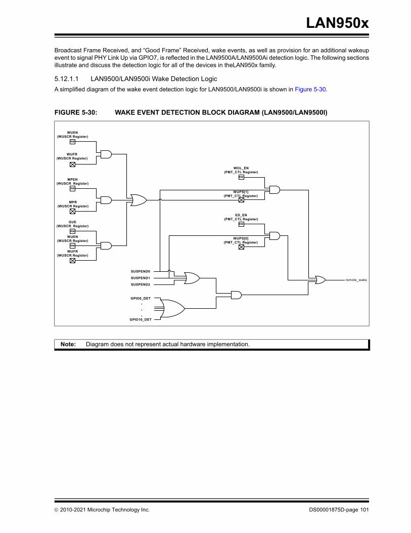
LAN950x
Broadcast Frame Received, and “Good Frame” Received, wake events, as well as provision for an additional wakeupevent to signal PHY Link Up via GPIO7, is reflected in the LAN9500A/LAN9500Ai detection logic. The following sectionsillustrate and discuss the detection logic for all of the devices in theLAN950x family.
5.12.1.1 LAN9500/LAN9500i Wake Detection Logic
A simplified diagram of the wake event detection logic for LAN9500/LAN9500i is shown in Figure 5-30.
FIGURE 5-30: WAKE EVENT DETECTION BLOCK DIAGRAM (LAN9500/LAN9500I)
Note: Diagram does not represent actual hardware implementation.
WOL_EN(PMT_CTL Register)
RW
WUPS[1](PMT_CTL Register)
SUSPEND0
ED_EN(PMT_CTL Register)
RW
WUPS[0](PMT_CTL Register)
WUEN(WUSCR Register)
RW
WUFR(WUSCR Register)
MPEN(WUSCR Register)
RW
MPR(WUSCR Register)
GPIO0_DET
SUSPEND1
SUSPEND2
.
.
.
remote_wake
GPIO10_DET
GUE(WUSCR Register)
RW
WUFR(WUSCR Register)
WUEN(WUSCR Register)
RW
2010-2021 Microchip Technology Inc. DS00001875D-page 101
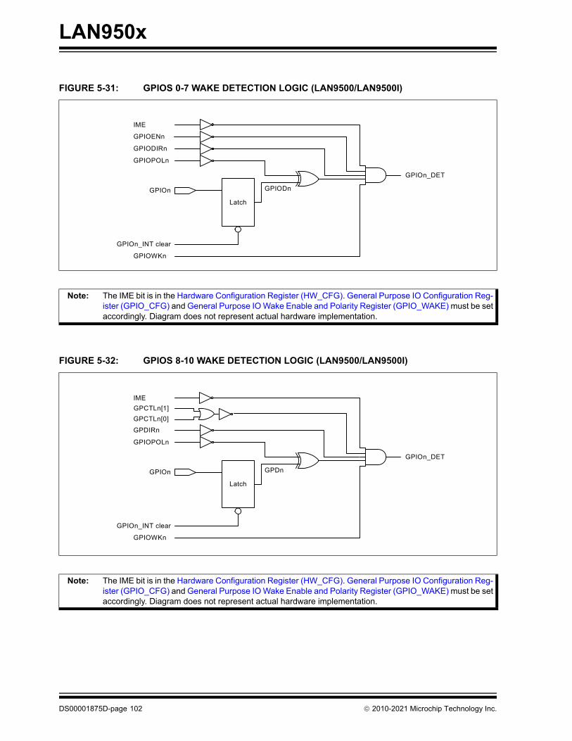
LAN950x
FIGURE 5-31: GPIOS 0-7 WAKE DETECTION LOGIC (LAN9500/LAN9500I)
Note: The IME bit is in the Hardware Configuration Register (HW_CFG). General Purpose IO Configuration Reg-ister (GPIO_CFG) and General Purpose IO Wake Enable and Polarity Register (GPIO_WAKE) must be setaccordingly. Diagram does not represent actual hardware implementation.
FIGURE 5-32: GPIOS 8-10 WAKE DETECTION LOGIC (LAN9500/LAN9500I)
Note: The IME bit is in the Hardware Configuration Register (HW_CFG). General Purpose IO Configuration Reg-ister (GPIO_CFG) and General Purpose IO Wake Enable and Polarity Register (GPIO_WAKE) must be setaccordingly. Diagram does not represent actual hardware implementation.
GPIOn_INT clear
GPIOn
GPIOPOLn
Latch
GPIODIRn
GPIODn
GPIOENn
GPIOWKn
GPIOn_DET
IME
GPIOn_INT clear
GPIOn
GPIOPOLn
Latch
GPDIRn
GPDn
GPCTLn[0]
GPIOWKn
GPIOn_DET
IME
GPCTLn[1]
DS00001875D-page 102 2010-2021 Microchip Technology Inc.
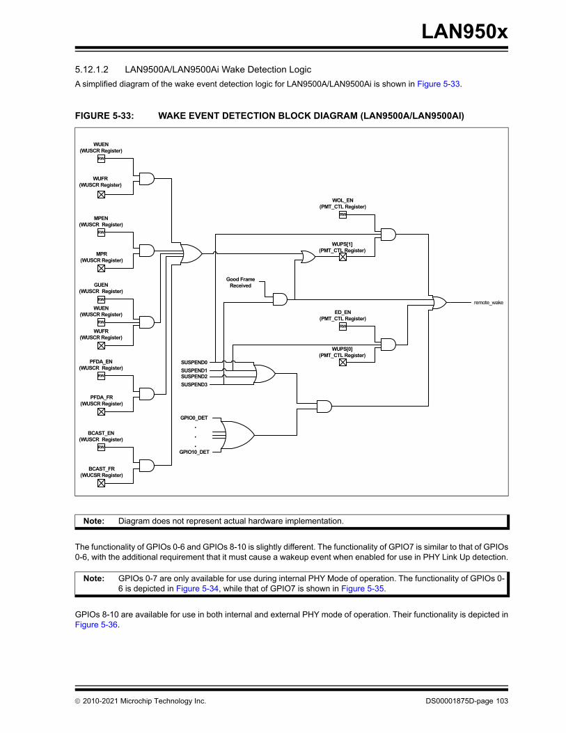
LAN950x
5.12.1.2 LAN9500A/LAN9500Ai Wake Detection Logic
A simplified diagram of the wake event detection logic for LAN9500A/LAN9500Ai is shown in Figure 5-33.
The functionality of GPIOs 0-6 and GPIOs 8-10 is slightly different. The functionality of GPIO7 is similar to that of GPIOs0-6, with the additional requirement that it must cause a wakeup event when enabled for use in PHY Link Up detection.
GPIOs 8-10 are available for use in both internal and external PHY mode of operation. Their functionality is depicted inFigure 5-36.
FIGURE 5-33: WAKE EVENT DETECTION BLOCK DIAGRAM (LAN9500A/LAN9500AI)
Note: Diagram does not represent actual hardware implementation.
Note: GPIOs 0-7 are only available for use during internal PHY Mode of operation. The functionality of GPIOs 0-6 is depicted in Figure 5-34, while that of GPIO7 is shown in Figure 5-35.
WOL_EN(PMT_CTL Register)
RW
WUPS[1](PMT_CTL Register)
SUSPEND0
ED_EN(PMT_CTL Register)
RW
WUPS[0](PMT_CTL Register)
WUEN(WUSCR Register)
RW
WUFR(WUSCR Register)
MPEN(WUSCR Register)
RW
MPR(WUSCR Register)
GPIO0_DET
GUEN(WUSCR Register)
RW
.
.
.
remote_wake
PFDA_EN(WUSCR Register)
RW
PFDA_FR(WUSCR Register)
BCAST_EN(WUSCR Register)
RW
BCAST_FR(WUCSR Register)
Good Frame Received
SUSPEND1SUSPEND2
SUSPEND3
WUFR(WUSCR Register)
WUEN(WUSCR Register)
RW
GPIO10_DET
2010-2021 Microchip Technology Inc. DS00001875D-page 103
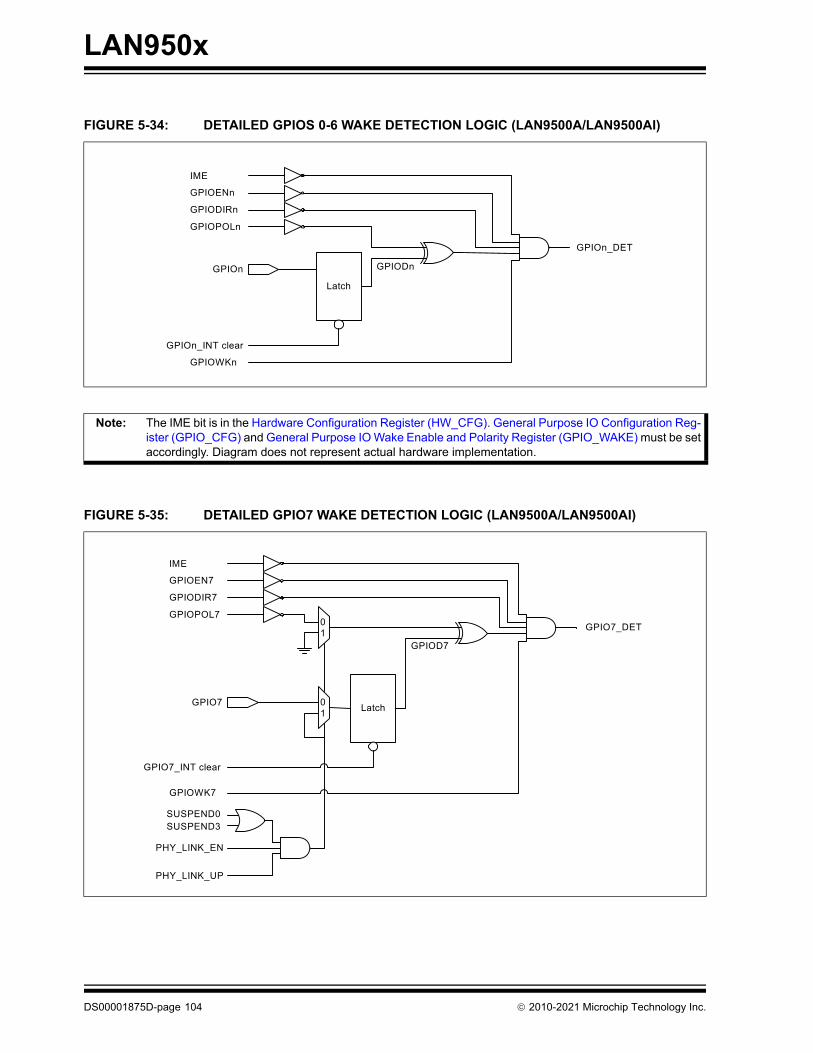
LAN950x
FIGURE 5-34: DETAILED GPIOS 0-6 WAKE DETECTION LOGIC (LAN9500A/LAN9500AI)
Note: The IME bit is in the Hardware Configuration Register (HW_CFG). General Purpose IO Configuration Reg-ister (GPIO_CFG) and General Purpose IO Wake Enable and Polarity Register (GPIO_WAKE) must be setaccordingly. Diagram does not represent actual hardware implementation.
FIGURE 5-35: DETAILED GPIO7 WAKE DETECTION LOGIC (LAN9500A/LAN9500AI)
GPIOn_INT clear
GPIOn
GPIOPOLn
Latch
GPIODIRn
GPIODn
GPIOENn
GPIOWKn
GPIOn_DET
IME
GPIO7_INT clear
GPIO7
GPIOPOL7
Latch
GPIODIR7
GPIOD7
GPIOEN7
GPIOWK7
IME
01
01
GPIO7_DET
SUSPEND0SUSPEND3
PHY_LINK_EN
PHY_LINK_UP
DS00001875D-page 104 2010-2021 Microchip Technology Inc.
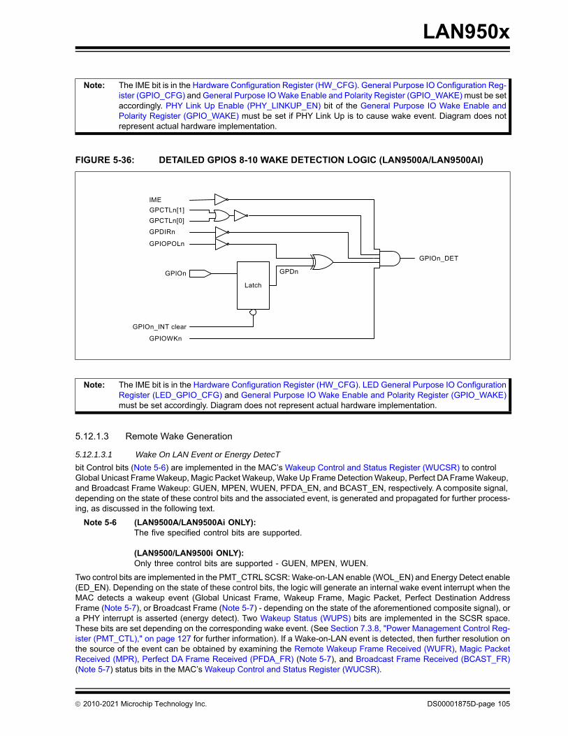
LAN950x
5.12.1.3 Remote Wake Generation
5.12.1.3.1 Wake On LAN Event or Energy DetecT
bit Control bits (Note 5-6) are implemented in the MAC’s Wakeup Control and Status Register (WUCSR) to control Global Unicast Frame Wakeup, Magic Packet Wakeup, Wake Up Frame Detection Wakeup, Perfect DA Frame Wakeup, and Broadcast Frame Wakeup: GUEN, MPEN, WUEN, PFDA_EN, and BCAST_EN, respectively. A composite signal, depending on the state of these control bits and the associated event, is generated and propagated for further process-ing, as discussed in the following text.
Note 5-6 (LAN9500A/LAN9500Ai ONLY):The five specified control bits are supported.
(LAN9500/LAN9500i ONLY):Only three control bits are supported - GUEN, MPEN, WUEN.
Two control bits are implemented in the PMT_CTRL SCSR: Wake-on-LAN enable (WOL_EN) and Energy Detect enable(ED_EN). Depending on the state of these control bits, the logic will generate an internal wake event interrupt when theMAC detects a wakeup event (Global Unicast Frame, Wakeup Frame, Magic Packet, Perfect Destination AddressFrame (Note 5-7), or Broadcast Frame (Note 5-7) - depending on the state of the aforementioned composite signal), ora PHY interrupt is asserted (energy detect). Two Wakeup Status (WUPS) bits are implemented in the SCSR space.These bits are set depending on the corresponding wake event. (See Section 7.3.8, "Power Management Control Reg-ister (PMT_CTL)," on page 127 for further information). If a Wake-on-LAN event is detected, then further resolution onthe source of the event can be obtained by examining the Remote Wakeup Frame Received (WUFR), Magic PacketReceived (MPR), Perfect DA Frame Received (PFDA_FR) (Note 5-7), and Broadcast Frame Received (BCAST_FR)(Note 5-7) status bits in the MAC’s Wakeup Control and Status Register (WUCSR).
Note: The IME bit is in the Hardware Configuration Register (HW_CFG). General Purpose IO Configuration Reg-ister (GPIO_CFG) and General Purpose IO Wake Enable and Polarity Register (GPIO_WAKE) must be setaccordingly. PHY Link Up Enable (PHY_LINKUP_EN) bit of the General Purpose IO Wake Enable andPolarity Register (GPIO_WAKE) must be set if PHY Link Up is to cause wake event. Diagram does notrepresent actual hardware implementation.
FIGURE 5-36: DETAILED GPIOS 8-10 WAKE DETECTION LOGIC (LAN9500A/LAN9500AI)
Note: The IME bit is in the Hardware Configuration Register (HW_CFG). LED General Purpose IO ConfigurationRegister (LED_GPIO_CFG) and General Purpose IO Wake Enable and Polarity Register (GPIO_WAKE)must be set accordingly. Diagram does not represent actual hardware implementation.
GPIOn_INT clear
GPIOn
GPIOPOLn
Latch
GPDIRn
GPDn
GPCTLn[0]
GPIOWKn
GPIOn_DET
IME
GPCTLn[1]
2010-2021 Microchip Technology Inc. DS00001875D-page 105
LAN950x
Note 5-7 Supported only by LAN9500A/LAN9500Ai.
Note 1: Wake-on-LAN events resulting in the generation of a remote-wake event may only occur when in SUS-PEND0 state.
2: Energy Detect events resulting in the generation of a remote-wake event may only occur when in SUS-PEND1 state.
Wakeup Frame detection must be enabled in the MAC before detection can occur. Likewise, the energy detect interruptmust be enabled in the PHY before this interrupt can be used as a wake event. If the device is properly configured, theinternal wake event interrupt will cause the assertion of the remote_wake signal on detection of a wake event.
5.12.1.3.2 Good Frame Detection (LAN9500A/LAN9500Ai ONLY)
To wakeup on reception of a frame passing the filtering constraints set solely by the MAC Control Register (MAC_CR),the enables for all Wake-On-LAN events contained in the Wakeup Control and Status Register (WUCSR) must becleared and the desired constraints must be selected in MAC_CR. The setting of the Wake-On-Lan Enable (WOL_EN)bit of the Power Management Control Register (PMT_CTL) is a “don’t care”. The logic will generate an internal wakeevent interrupt when the MAC detects a frame passing the filtering constraints (“Good Frame”). The Wake-On-LAN bitof the Wakeup Status (WUPS) field of the Power Management Control Register (PMT_CTL) is used to signal wakeupdue to reception of the “Good Frame”.
5.12.1.3.3 GPIO Pin
GPIO pins 0 through 10 may cause the generation of a remote-wake event when properly configured and in any of theSUSPEND states. GPIO pins 0 through 7 each have a control bit (GPIOENx, 0<=x<=7) in the General Purpose IO Con-figuration Register (GPIO_CFG) that is used to enable the GPIO pin to generate a remote-wake event. GPIO pins 8through 10 have no specific enable bit. The corresponding enable signal for these pins (GPIOENy, 8<=y<=10) is derivedfrom the manner in which the pin is programmed. Ten GPIO wakeup status bits (GPIOWKy, 8<=y<=10) are available todetermine the source of the event.
5.12.1.3.4 PHY Link Up (LAN9500A/LAN9500Ai ONLY)
GPIO7 may be programmed to signal a wakeup in SUSPEND0 or SUSPEND3 state on occurrence of a PHY Link Up.The PHY Link Up Enable (PHY_LINKUP_EN) bit of the General Purpose IO Wake Enable and Polarity Register (GPI-O_WAKE) must be set to use GPIO7 for this purpose. When used in this mode, the signal connected to the device’s pinis ignored.
5.12.2 ENABLING WAKE EVENTS
5.12.2.1 Enabling GPIO Wake Events
The Host system must perform the following steps to enable the device to assert a remote_wake event on detection ofa GPIO wake event.
1. The GPIO pin is programmed to facilitate generation of the wake event. If the pin is one of GPIO0 through GPIO7,the pin must be enabled to generate the event (GPIOENx must be clear in the General Purpose IO ConfigurationRegister (GPIO_CFG)). If the pin is one of GPIO8 through GPIO10, the pin must be programmed as a input GPIOpin (the GPCTL and GPDIR fields for the pin in the LED General Purpose IO Configuration Register (LED_GPI-O_CFG) must be set to 00b and 0, respectively). In addition, the pin must be enabled for wakeup and its desiredpolarity specified in the GPIO Wake 0-10 (GPIOWKn) and GPIO Polarity 0-10 (GPIOPOLn) fields, respectively,of the General Purpose IO Wake Enable and Polarity Register (GPIO_WAKE).
2. The Host places the device in the any one of the SUSPEND states by setting the Suspend Mode (SUSPEND_-MODE) field of the Power Management Control Register (PMT_CTL) to indicate the desired suspend state, thensends suspend signaling.
On detection of an enabled GPIO wake event, the device will transition back to the NORMAL state and signal aremote_wake event. The Host may then examine the GPIO [10:0] (GPIOx_INT) status bits of the Interrupt Status Reg-ister (INT_STS) to determine the source of the wakeup.
Note: “Good Frame” reception resulting in the generation of a remote-wake event may only occur when in theSUSPEND3 state.
DS00001875D-page 106 2010-2021 Microchip Technology Inc.
LAN950x
5.12.2.2 Enabling WOL Wake Events
The Host system must perform the following steps to enable the device to assert a remote_wake event on detection ofa Wake on LAN event.
1. All transmit and receive operations must be halted:
a) All pending Ethernet TX and RX operations must be completed.
b) The MAC must be halted.
2. The MAC must be configured to detect the desired wake event. This process is explained in Section 5.5.5,"Wakeup Frame Detection," on page 59 for Wakeup Frames and in Section 5.5.6, "Magic Packet Detection," onpage 63 for Magic Packets.
(LAN9500A/LAN9500Ai ONLY):Configuring Perfect DA and Broadcast Frame wakeup detection is analogous and requires the Perfect DAWakeup Enable (PFDA_EN) or Broadcast Wakeup Enable (BCAST_EN) bit to be set in the Wakeup Control andStatus Register (WUCSR).
3. Bit 1 of the Wakeup Status (WUPS[1]) in the Power Management Control Register (PMT_CTL) must be clearedsince a set bit will cause the immediate assertion of wake event when the Wake-On-Lan Enable (WOL_EN) bitis set. The WUPS[1] bit will not clear if the internal MAC wakeup event is asserted.
4. Set the Wake-On-Lan Enable (WOL_EN) bit in the Power Management Control Register (PMT_CTL).
5. The Host places the device in the SUSPEND0 state by setting the Suspend Mode (SUSPEND_MODE) field inthe Power Management Control Register (PMT_CTL) to 00b, to indicate the desired suspend state, then sendssuspend signaling.
On detection of an enabled event, the device will transition back to the NORMAL state and signal a remote_wake event.The software will then examine the Suspend Mode (SUSPEND_MODE) field of the Power Management Control Reg-ister (PMT_CTL). Upon discovering wakeup occurred from SUSPEND0 state, the status bits of the WUCSR registermay be examined to determine the particular event that caused the wakeup.
5.12.2.3 Enabling Link Status Change (Energy Detect) Wake Events
The Host system must perform the following steps to enable the device to assert a remote_wake event on detection ofan Ethernet link status change.
1. All transmit and receive operations must be halted:
a) All pending Ethernet TX and RX operations must be completed.
b) The MAC must be halted.
2. The PHY must be enabled for the energy detect power down mode This is done by clearing the EDPWRDOWNbit in the PHY’s Mode Control/Status Register. Enabling the energy detect power-down mode places the PHY ina reduced power state. In this mode of operation the PHY is not capable of receiving or transmitting Ethernetdata. In this state, the PHY will assert its internal interrupt if it detects Ethernet activity. Refer to Section 5.6.8.2,"Energy Detect Power-Down (EDPD)," on page 78 for more information.
3. Bit 0 of the Wakeup Status (WUPS[0]) in the Power Management Control Register (PMT_CTL) must be cleared,since a set bit will cause the immediate assertion of wake event when Energy-Detect Enable (ED_EN) is set. TheWUPS[0] bit will not clear if the internal PHY interrupt is asserted.
4. Set the Energy-Detect Enable (ED_EN) bit in the Power Management Control Register (PMT_CTL).
5. The Host places the device in the SUSPEND1 state by setting the Suspend Mode (SUSPEND_MODE) field inthe Power Management Control Register (PMT_CTL) to 01b, to indicate the desired suspend state, then sendssuspend signaling.
On detection of Ethernet activity (energy), the device will transition back to the NORMAL state and signal aremote_wake event.
2010-2021 Microchip Technology Inc. DS00001875D-page 107
LAN950x
5.12.2.4 Enabling PHY Link Up Wake Events (LAN9500A/LAN9500Ai ONLY)
The Host system must perform the following steps to enable the device to assert a remote_wake event on detection ofPHY Link Up.
1. The system software determines that the link is down by periodically polling the Link Status bit of the Basic StatusRegister.
Alternatively, the driver can detect assertion of the PHY_INT bit via the interrupt control endpoint. The driver mayalso detect PHY interrupt assertion by polling the Interrupt Status Register (INT_STS). It then reads the BasicStatus Register and finds the Link Status bit is deasserted.
2. On finding the link down, the Host configures the device to wake up on PHY Link Up and signal the event usingGPIO7 as follows:
a) The PHY Link Up Enable (PHY_LINKUP_EN) bit is set in the General Purpose IO Wake Enable and PolarityRegister (GPIO_WAKE) to enable GPIO7 use in signaling the PHY Link Up event. The GPIOWK7 bit is alsoset in the register to permit its use in wake event generation. The setting of GPIOPOL7 is a “don’t care”.
b) The following additional parameters for GPIO7 must be configured in the General Purpose IO ConfigurationRegister (GPIO_CFG) : GPIOEN7 = 0, GPIODIR7 = 0, GPIOBUF7 = “don’t care”.
3. The GPIO7_INT bit in the Interrupt Status Register (INT_STS) must be cleared, since a set bit will cause theimmediate assertion of the wake event.
4. The Host places the device in the SUSPEND0 or SUSPEND3 state, as appropriate, by setting the Suspend Mode(SUSPEND_MODE) field in the Power Management Control Register (PMT_CTL) to 00b or 11b, to indicate thedesired suspend state. The Host then sends suspend signaling.
On detection of PHY Link Up, the device will transition back to the NORMAL state and signal a remote_wake event. TheHost, in trying to determine the cause of the wake event, may then examine the GPIO [10:0] (GPIOx_INT) status bits ofthe Interrupt Status Register (INT_STS). On finding GPIO7_INT set, the software will then use the Suspend Mode (SUS-PEND_MODE) field of the Power Management Control Register (PMT_CTL) and the value of the PHY Link Up Enable(PHY_LINKUP_EN) bit to determine a PHY Link Up wake event occurred.
5.12.2.5 Enabling “Good Frame” Wake Events (LAN9500A/LAN9500Ai ONLY)
The Host system must perform the following steps to enable the device to assert a remote_wake event on detection ofa “Good Frame”.
1. The MAC filtering is configured by setting the desired constraints in the MAC Control Register (MAC_CR). AllWake-On-LAN events contained in the Wakeup Control and Status Register (WUCSR) must be disabled. Thesetting of the Wake-On-Lan Enable (WOL_EN) bit of the Power Management Control Register (PMT_CTL) is a“don’t care”.
2. Bit 1 of the Wakeup Status (WUPS[1]) in the Power Management Control Register (PMT_CTL) must be clearedsince a set bit will cause the immediate assertion of wake event. The WUPS[1] bit will not clear if the internalMAC wakeup event is asserted.
3. The Host places the device in the SUSPEND3 state by setting the Suspend Mode (SUSPEND_MODE) field inthe Power Management Control Register (PMT_CTL) to 11b, to indicate the desired suspend state, then sendssuspend signaling.
On detection of a “Good Frame”, the device will transition back to the NORMAL state and signal a remote_wake event.The software will then examine the Suspend Mode (SUSPEND_MODE) field of the Power Management Control Reg-ister (PMT_CTL). Upon discovering wakeup occurred from SUSPEND3 state, the host may perform desired processingas a result of receiving the “Good Frame”.
5.12.3 NETDETACH (LAN9500A/LAN9500AI ONLY)
NetDetach is a mode of operation where the device detaches from the USB bus after the Ethernet cable is disconnected.This is advantageous for mobile devices, as an attached USB device prevents the Host CPU from entering the APCIC3 state. Allowing the CPU to enter the C3 state maximizes battery life.
When detached, the device’s power state is essentially the same as the SUSPEND1 state. After the Ethernet cable isreconnected, or a programmed GPIO pin asserts, the device automatically attaches to the USB bus. GPIO pin assertionis supported so that this feature can be used with external PHY mode. In this case, the external PHY’s link LED wouldbe connected to a GPIO.
DS00001875D-page 108 2010-2021 Microchip Technology Inc.
LAN950x
The NetDetach feature requires assistance of the driver. The driver will monitor the link status of the Ethernet PHY andprogram the device appropriately to detach and re-attach to the USB bus upon link up. The following steps illustrate thisprocess:
1. User disconnects the Ethernet cable.
2. Driver detects assertion of the PHY_INT bit via the interrupt control endpoint. The driver may also detect PHYinterrupt assertion by polling the Interrupt Status Register (INT_STS).
3. Driver reads the Basic Status Register and finds the Link Status bit is deasserted.
4. At this point, the Driver may place the Ethernet PHY into either the Energy Detect Power-Down mode or the PHYLink Up Detection mode. Section 5.12.2.3, "Enabling Link Status Change (Energy Detect) Wake Events," onpage 107 and Section 5.12.2.4, "Enabling PHY Link Up Wake Events (LAN9500A/LAN9500Ai ONLY)," onpage 108 provide detailed instructions for programming these modes.
5. Driver sets the NetDetach Enable (SMDET_EN) bit in the Hardware Configuration Register (HW_CFG).
6. The device then detaches from the USB bus and disables the USB PLL. The driver is unloaded at this point andcan no longer communicate with the device.
7. At some point in the future, the Ethernet cable is reconnected, or an appropriately configured GPIO pin isasserted.
8. The device attaches to the USB bus.
9. The driver is loaded and the device is configured by the driver. The driver examines the NetDetach Status(SMDET_STS) bit in the Hardware Configuration Register (HW_CFG) to determine if it was reloaded as a resultof coming back from a NetDetach operation or for some other reason.
5.13 Resets
The device has the following chip level reset sources:
• Power-On Reset (POR)
• External Chip Reset (nRESET)
• Lite Reset (LRST)
• Soft Reset (SRST)
• USB Reset
• PHY Software Reset
• nTRST
• VBUS_DET
5.13.1 POWER-ON RESET (POR)
A Power-On reset occurs whenever power is initially applied to the device, or if power is removed and reapplied to thedevice. A timer within the device will assert the internal reset for approximately 22mS.
Note 1: The EEPROM contents are loaded by this reset.
2: After the assertion of the POR, the internal Ethernet PHY is put into general power down mode.
5.13.2 EXTERNAL CHIP RESET (NRESET)
A hardware reset will occur when the nRESET pin is driven low. The READY bit in the PMT_CTRL register can be readby the Host, and will read back a ‘0’ until the hardware reset is complete. Upon completion of the hardware reset, theREADY bit in PMT_CTRL is set high.
After the “READY” bit is set, the device can be configured via its control registers. The nRESET pin is pulled-high inter-nally by the device and can be left unconnected if unused. If used, nRESET must be driven low for a minimum periodas defined in Section 8.6.3, "Reset and Configuration Strap Timing," on page 197. If nRESET is unused, the device mustbe reset following power-up via a soft reset (SRST).
Note 1: After the assertion of nRESET, the internal Ethernet PHY is put into general power down mode.
2: nRESET is ignored when the device is in the UNPOWERED state. As in the UNPOWERED state the entirechip is held in reset.
2010-2021 Microchip Technology Inc. DS00001875D-page 109
LAN950x
5.13.3 LITE RESET (LRST)
This reset is initiated via the LRST bit in the Section 7.3.5, "Hardware Configuration Register (HW_CFG)". It will resetthe entire chip with the exception of the USB Device Controller and the USB PHY (UDC, parts of the CTL, and the USBPHY). The PLL is not turned off.
Note 1: This reset does not cause the USB contents from the EEPROM to be reloaded.
2: This reset does not place the device into the Unconfigured state.
3: After the LRST, the USB pipes corresponding to the Bulk In, Bulk Out, and Interrupt endpoints must be reset.This process entails clearing the device’s ENDPOINT_HALT feature and resetting the data toggle on thehost side.
5.13.4 SOFT RESET (SRST)
A Soft reset is initiated by writing a ‘1’ to bit 0 of the HW_CFG register (SRST). This self-clearing bit will return to ‘0’ afterapproximately 2 s, at which time the Soft Reset is complete. Soft reset does not clear control register bits marked asNASR.
Note 1: The EEPROM contents are reloaded by this reset.
2: After the assertion of the SRST the internal Ethernet PHY is put into general power down mode.
Writing SRST=1 will cause the device to disconnect from the USB shortly after the first good OUT Data pkt during theData Phase. In HS mode, a brief delay will allow enough time for the device to send the ACK for the Data Stage, but thedevice will be disconnected (causing a 3-strikes timeout failure) for any next transaction (e.g., the Status Stage, or arepeated Data Stage, if there were any bus errors). In FS mode, the brief delay will be short enough that the device willdisconnect during the ACK pkt, causing CRC, bit-stuff, etc. errors on USB. To the USB Host, the aforementioned behav-iors are the same as what happens during any Surprise Removal of a USB Device. This behavior is completely normal,and a compliant Host must be tolerant of it.
5.13.5 USB RESET
A USB reset causes a reset of the entire chip with the exception of the USB Device Controller and the USB PHY (UDC,parts of the CTL, and the USB PHY). The PLL is not turned off. It will occur after a POR, nRESET, or SRST (These willall force disconnects of the USB bus). After a USB reset, the READY bit in the PMT_CTRL register can be read by theHost and will read back a ‘0’ until the EEPROM contents are loaded (provided one is present). Upon completion of theEEPROM contents load, the READY bit in PMT_CTRL is set high, and the device can be configured via its control reg-isters.
Note 1: This reset does not cause the USB contents from the EEPROM to be reloaded. Only the MAC address isreloaded.
2: After the assertion of the USB Reset the internal Ethernet PHY is put into general power down mode.
5.13.6 PHY SOFTWARE RESET
The Ethernet PHY can be reset via two software-initiated resets. Please refer to Section 5.6.9, "PHY Resets," onpage 78 for details.
5.13.7 NTRST
This active-low reset is used by the TAP controller.
5.13.8 VBUS_DET
The removal of USB power causes the device to transition to the UNPOWERED state. The chip is held in reset while inthe UNPOWERED state.
Note 1: After VBUS_DET is asserted, the contents of the EEPROM are reloaded.
2: After transitioning out of the UNPOWERED state, the internal Ethernet PHY is in general power down mode.
DS00001875D-page 110 2010-2021 Microchip Technology Inc.
LAN950x
5.14 Configuration Straps
Configuration straps are multi-function pins that are driven as outputs during normal operation. During a Power-OnReset (POR) or a External Chip Reset (nRESET), these outputs are tri-stated. The high or low state of the signal islatched following de-assertion of the reset and is used to determine the default configuration of a particular feature. Con-figuration strap signals are noted in Section 3.0, "Pin Description and Configuration," on page 11.
Configuration straps are latched as a result of a Power-On Reset (POR) or a External Chip Reset (nRESET).
bit Configuration straps include internal resistors in order to prevent the signal from floating when unconnected. If a par-ticular configuration strap is connected to a load, an external pull-up or pull-down should be used to augment the internal resistor to ensure that it reaches the required voltage level prior to latching. The internal resistor can also be overridden by the addition of an external resistor.
Note 1: The system designer must ensure that configuration straps meet the timing requirements specified in Sec-tion 8.6.3, "Reset and Configuration Strap Timing," on page 197 and Section 8.6.2, "Power-On Configura-tion Strap Valid Timing," on page 196. If configuration straps are not at the correct voltage level prior to beinglatched, the device may capture incorrect strap values.
2: Configuration straps must never be driven as inputs. If required, configuration straps can be augmented, oroverridden with external resistors.
2010-2021 Microchip Technology Inc. DS00001875D-page 111
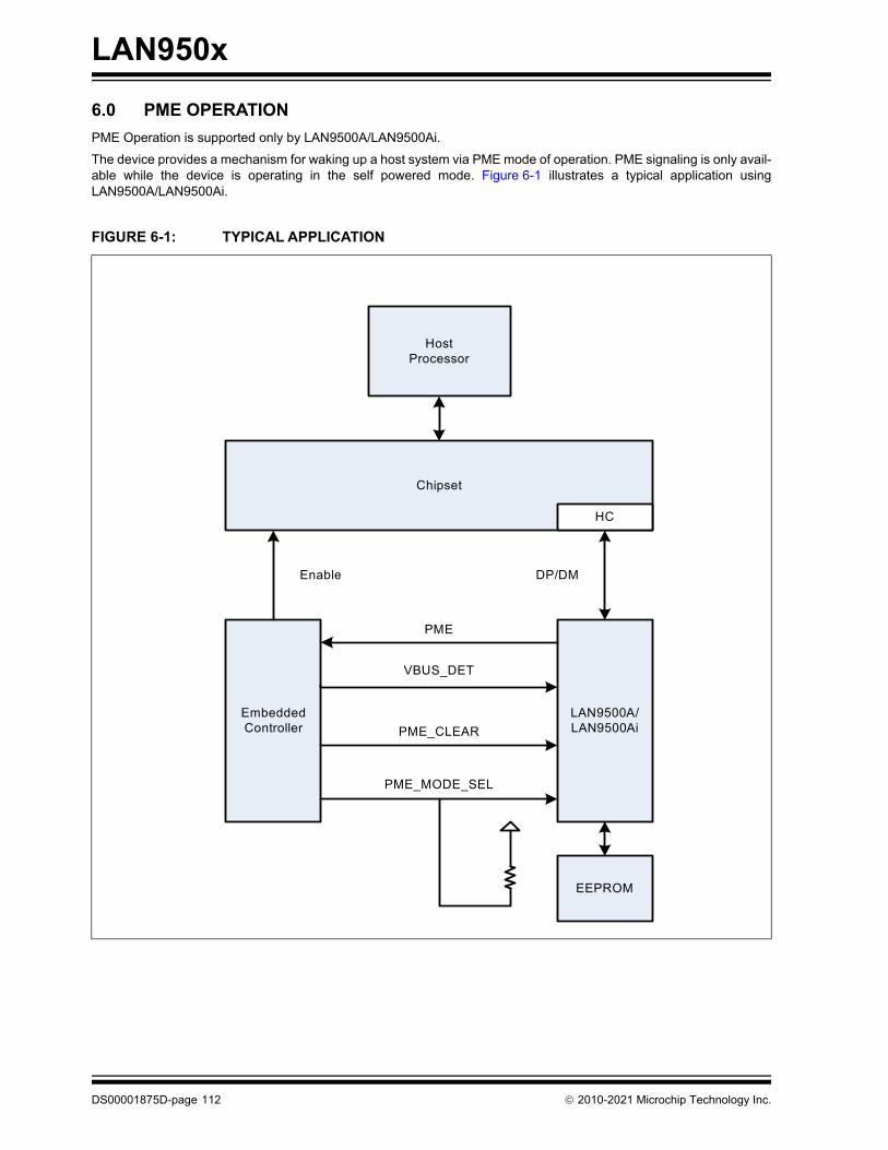
LAN950x
6.0 PME OPERATION
PME Operation is supported only by LAN9500A/LAN9500Ai.
The device provides a mechanism for waking up a host system via PME mode of operation. PME signaling is only avail-able while the device is operating in the self powered mode. Figure 6-1 illustrates a typical application usingLAN9500A/LAN9500Ai.
FIGURE 6-1: TYPICAL APPLICATION
LAN9500A/LAN9500Ai
Embedded Controller
Chipset
DP/DM
PME
PME_MODE_SEL
Enable
HC
PME_CLEAR
VBUS_DET
EEPROM
HostProcessor
DS00001875D-page 112 2010-2021 Microchip Technology Inc.
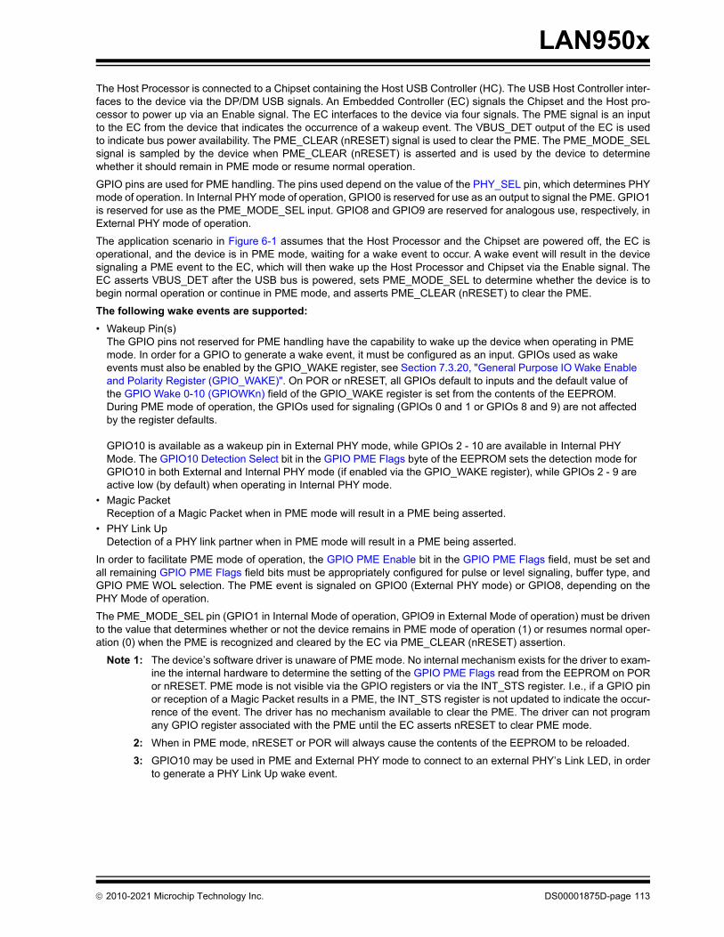
LAN950x
The Host Processor is connected to a Chipset containing the Host USB Controller (HC). The USB Host Controller inter-faces to the device via the DP/DM USB signals. An Embedded Controller (EC) signals the Chipset and the Host pro-cessor to power up via an Enable signal. The EC interfaces to the device via four signals. The PME signal is an inputto the EC from the device that indicates the occurrence of a wakeup event. The VBUS_DET output of the EC is usedto indicate bus power availability. The PME_CLEAR (nRESET) signal is used to clear the PME. The PME_MODE_SELsignal is sampled by the device when PME_CLEAR (nRESET) is asserted and is used by the device to determinewhether it should remain in PME mode or resume normal operation.
GPIO pins are used for PME handling. The pins used depend on the value of the PHY_SEL pin, which determines PHYmode of operation. In Internal PHY mode of operation, GPIO0 is reserved for use as an output to signal the PME. GPIO1is reserved for use as the PME_MODE_SEL input. GPIO8 and GPIO9 are reserved for analogous use, respectively, inExternal PHY mode of operation.
The application scenario in Figure 6-1 assumes that the Host Processor and the Chipset are powered off, the EC isoperational, and the device is in PME mode, waiting for a wake event to occur. A wake event will result in the devicesignaling a PME event to the EC, which will then wake up the Host Processor and Chipset via the Enable signal. TheEC asserts VBUS_DET after the USB bus is powered, sets PME_MODE_SEL to determine whether the device is tobegin normal operation or continue in PME mode, and asserts PME_CLEAR (nRESET) to clear the PME.
The following wake events are supported:
• Wakeup Pin(s)The GPIO pins not reserved for PME handling have the capability to wake up the device when operating in PME mode. In order for a GPIO to generate a wake event, it must be configured as an input. GPIOs used as wake events must also be enabled by the GPIO_WAKE register, see Section 7.3.20, "General Purpose IO Wake Enable and Polarity Register (GPIO_WAKE)". On POR or nRESET, all GPIOs default to inputs and the default value of the GPIO Wake 0-10 (GPIOWKn) field of the GPIO_WAKE register is set from the contents of the EEPROM. During PME mode of operation, the GPIOs used for signaling (GPIOs 0 and 1 or GPIOs 8 and 9) are not affected by the register defaults.
GPIO10 is available as a wakeup pin in External PHY mode, while GPIOs 2 - 10 are available in Internal PHY Mode. The GPIO10 Detection Select bit in the GPIO PME Flags byte of the EEPROM sets the detection mode for GPIO10 in both External and Internal PHY mode (if enabled via the GPIO_WAKE register), while GPIOs 2 - 9 are active low (by default) when operating in Internal PHY mode.
• Magic PacketReception of a Magic Packet when in PME mode will result in a PME being asserted.
• PHY Link UpDetection of a PHY link partner when in PME mode will result in a PME being asserted.
In order to facilitate PME mode of operation, the GPIO PME Enable bit in the GPIO PME Flags field, must be set andall remaining GPIO PME Flags field bits must be appropriately configured for pulse or level signaling, buffer type, andGPIO PME WOL selection. The PME event is signaled on GPIO0 (External PHY mode) or GPIO8, depending on thePHY Mode of operation.
The PME_MODE_SEL pin (GPIO1 in Internal Mode of operation, GPIO9 in External Mode of operation) must be drivento the value that determines whether or not the device remains in PME mode of operation (1) or resumes normal oper-ation (0) when the PME is recognized and cleared by the EC via PME_CLEAR (nRESET) assertion.
Note 1: The device’s software driver is unaware of PME mode. No internal mechanism exists for the driver to exam-ine the internal hardware to determine the setting of the GPIO PME Flags read from the EEPROM on PORor nRESET. PME mode is not visible via the GPIO registers or via the INT_STS register. I.e., if a GPIO pinor reception of a Magic Packet results in a PME, the INT_STS register is not updated to indicate the occur-rence of the event. The driver has no mechanism available to clear the PME. The driver can not programany GPIO register associated with the PME until the EC asserts nRESET to clear PME mode.
2: When in PME mode, nRESET or POR will always cause the contents of the EEPROM to be reloaded.
3: GPIO10 may be used in PME and External PHY mode to connect to an external PHY’s Link LED, in orderto generate a PHY Link Up wake event.
2010-2021 Microchip Technology Inc. DS00001875D-page 113
LAN950x
Figure 6-2 flowcharts PME operation while in Internal PHY mode. The following conditions hold:
EEPROM Configuration:
• GPIO PME Enable = 1 (enabled)
• GPIO PME Configuration = 0 (PME signaled via level on GPIO pin)
• GPIO PME Length = 0 (NA)
• GPIO PME Polarity = 1 (high level signals event)
• GPIO PME Buffer Type = 1 (Push-Pull)
• GPIO PME WOL Select = 0 (Magic Packet wakeup)
• GPIO10 Detection Select = 0 (Active-low detection)
• Power Method = 1 (self powered)
• MAC address for Magic Packet
PME signaling configuration (as determined by PHY Mode)
• GPIO0 signals PME
• GPIO1 is PME_MODE_SEL
Note: A POR occurring when PME_MODE_SEL = 1 and an EEPROM present with the GPIO PME Enable setresults in the device entering PME Mode.
DS00001875D-page 114 2010-2021 Microchip Technology Inc.
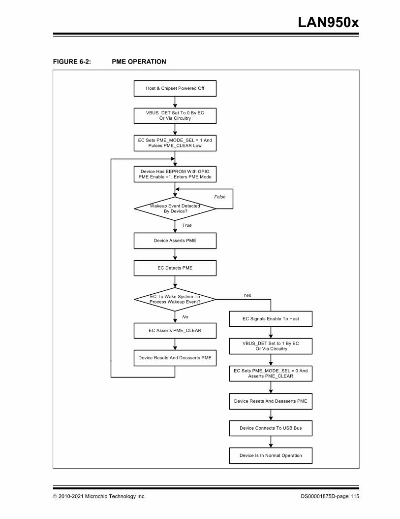
LAN950x
FIGURE 6-2: PME OPERATION
Wakeup Event Detected By Device?
Host & Chipset Powered Off
Device Asserts PME
True
False
VBUS_DET Set To 0 By ECOr Via Circuitry
EC Sets PME_MODE_SEL = 1 And Pulses PME_CLEAR Low
Device Has EEPROM With GPIO PME Enable =1, Enters PME Mode
EC Detects PME
EC To Wake System To Process Wakeup Event?
EC Asserts PME_CLEAR
Device Resets And Deasserts PME
VBUS_DET Set to 1 By EC Or Via Circuitry
EC Sets PME_MODE_SEL = 0 And Asserts PME_CLEAR
EC Signals Enable To Host
Device Resets And Deasserts PME
Device Connects To USB Bus
Device Is In Normal Operation
Yes
No
2010-2021 Microchip Technology Inc. DS00001875D-page 115
LAN950x
7.0 REGISTER DESCRIPTIONS
7.1 Register Nomenclature
Table 7-1 describes the register bit attributes used throughout this document.
7.2 Register Memory Map
TABLE 7-1: REGISTER BIT TYPES
Register BitType Notation
Register Bit Description
R Read: A register or bit with this attribute can be read.
W Write: A register or bit with this attribute can be written.
RO Read only: Read only. Writes have no effect.
RS Read to Set: This bit is set on read.
WO Write only: If a register or bit is write-only, reads will return unspecified data.
WC Write One to Clear: writing a one clears the value. Writing a zero has no effect.
WAC Write Anything to Clear: writing anything clears the value.
RC Read to Clear: Contents is cleared after the read. Writes have no effect.
LL Latch Low: Clear on read of register.
LH Latch High: Clear on read of register.
SC Self-Clearing: Contents is self-cleared after the being set. Writes of zero have no effect. Contents can be read.
RO/LH Read Only, Latch High: This mode is used by the Ethernet PHY registers. Bits with this attribute will stay high until the bit is read. After it a read, the bit will remain high, but will change to low if the condition that caused the bit to go high is removed. If the bit has not been read the bit will remain high regardless of if its cause has been removed.
NASR Not Affected by Software Reset. The state of NASR bits does not change on assertion of a software reset.
RESERVED Reserved Field: Reserved fields must be written with zeros, unless otherwise indicated, to ensure future compatibility. The value of reserved bits is not guaranteed on a read.
TABLE 7-2: LAN950X REGISTER MEMORY MAP
Address Symbol Register Name
000h - 0FFh SCSR System Control and Status Registers
100h - 1FCh MCSR MAC Control and Status Registers
DS00001875D-page 116 2010-2021 Microchip Technology Inc.
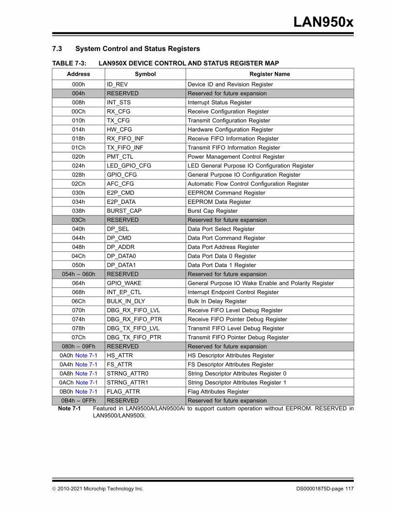
LAN950x
7.3 System Control and Status Registers
Note 7-1 Featured in LAN9500A/LAN9500Ai to support custom operation without EEPROM. RESERVED inLAN9500/LAN9500i.
TABLE 7-3: LAN950X DEVICE CONTROL AND STATUS REGISTER MAP
Address Symbol Register Name
000h ID_REV Device ID and Revision Register
004h RESERVED Reserved for future expansion
008h INT_STS Interrupt Status Register
00Ch RX_CFG Receive Configuration Register
010h TX_CFG Transmit Configuration Register
014h HW_CFG Hardware Configuration Register
018h RX_FIFO_INF Receive FIFO Information Register
01Ch TX_FIFO_INF Transmit FIFO Information Register
020h PMT_CTL Power Management Control Register
024h LED_GPIO_CFG LED General Purpose IO Configuration Register
028h GPIO_CFG General Purpose IO Configuration Register
02Ch AFC_CFG Automatic Flow Control Configuration Register
030h E2P_CMD EEPROM Command Register
034h E2P_DATA EEPROM Data Register
038h BURST_CAP Burst Cap Register
03Ch RESERVED Reserved for future expansion
040h DP_SEL Data Port Select Register
044h DP_CMD Data Port Command Register
048h DP_ADDR Data Port Address Register
04Ch DP_DATA0 Data Port Data 0 Register
050h DP_DATA1 Data Port Data 1 Register
054h – 060h RESERVED Reserved for future expansion
064h GPIO_WAKE General Purpose IO Wake Enable and Polarity Register
068h INT_EP_CTL Interrupt Endpoint Control Register
06Ch BULK_IN_DLY Bulk In Delay Register
070h DBG_RX_FIFO_LVL Receive FIFO Level Debug Register
074h DBG_RX_FIFO_PTR Receive FIFO Pointer Debug Register
078h DBG_TX_FIFO_LVL Transmit FIFO Level Debug Register
07Ch DBG_TX_FIFO_PTR Transmit FIFO Pointer Debug Register
080h – 09Fh RESERVED Reserved for future expansion
0A0h Note 7-1 HS_ATTR HS Descriptor Attributes Register
0A4h Note 7-1 FS_ATTR FS Descriptor Attributes Register
0A8h Note 7-1 STRNG_ATTR0 String Descriptor Attributes Register 0
0ACh Note 7-1 STRNG_ATTR1 String Descriptor Attributes Register 1
0B0h Note 7-1 FLAG_ATTR Flag Attributes Register
0B4h – 0FFh RESERVED Reserved for future expansion
2010-2021 Microchip Technology Inc. DS00001875D-page 117
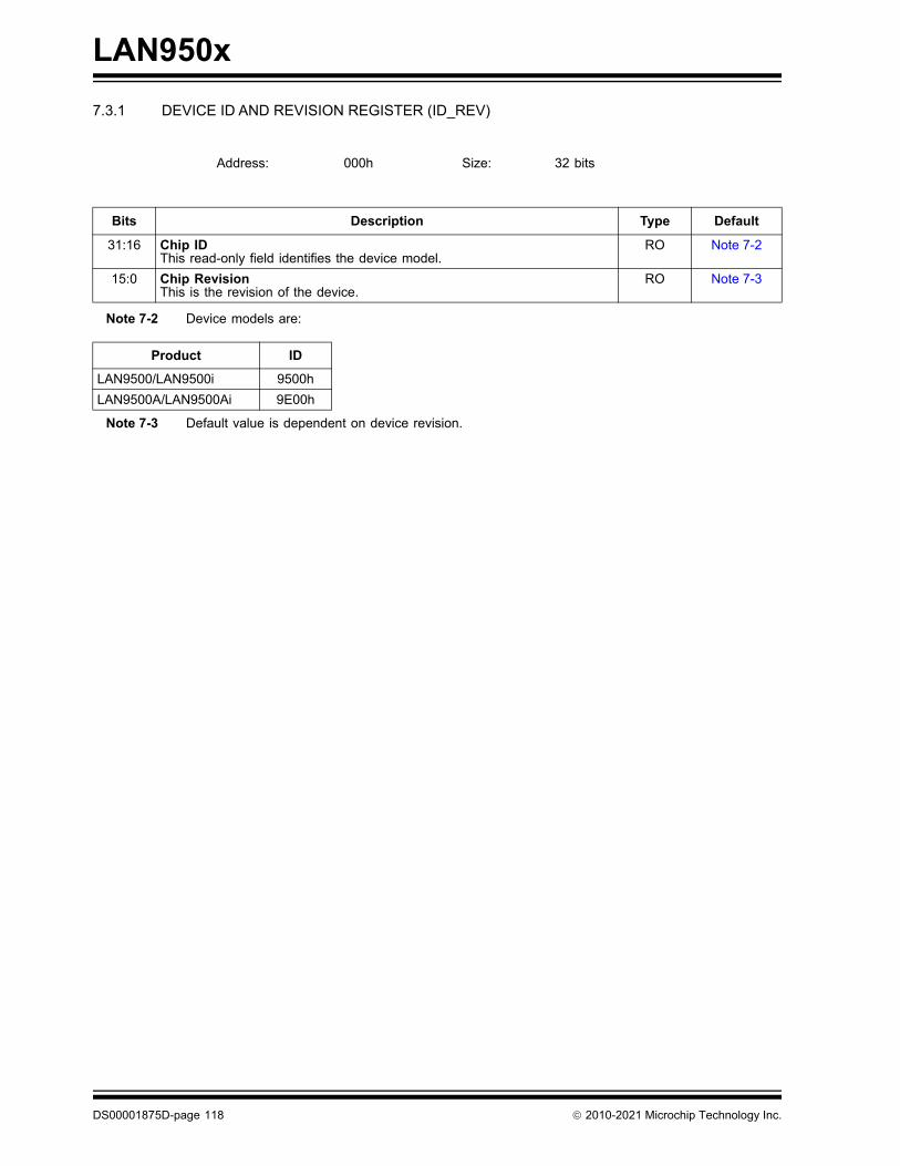
LAN950x
7.3.1 DEVICE ID AND REVISION REGISTER (ID_REV)
Note 7-2 Device models are:
Note 7-3 Default value is dependent on device revision.
Address: 000h Size: 32 bits
Bits Description Type Default
31:16 Chip IDThis read-only field identifies the device model.
RO Note 7-2
15:0 Chip RevisionThis is the revision of the device.
RO Note 7-3
Product ID
LAN9500/LAN9500i 9500h
LAN9500A/LAN9500Ai 9E00h
DS00001875D-page 118 2010-2021 Microchip Technology Inc.
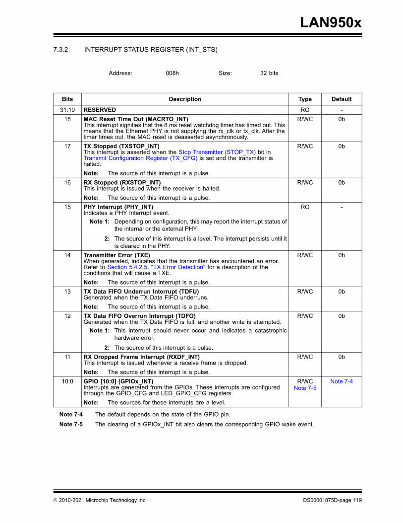
LAN950x
7.3.2 INTERRUPT STATUS REGISTER (INT_STS)
Note 7-4 The default depends on the state of the GPIO pin.
Note 7-5 The clearing of a GPIOx_INT bit also clears the corresponding GPIO wake event.
Address: 008h Size: 32 bits
Bits Description Type Default
31:19 RESERVED RO -
18 MAC Reset Time Out (MACRTO_INT)This interrupt signifies that the 8 ms reset watchdog timer has timed out. This means that the Ethernet PHY is not supplying the rx_clk or tx_clk. After the timer times out, the MAC reset is deasserted asynchronously.
R/WC 0b
17 TX Stopped (TXSTOP_INT)This interrupt is asserted when the Stop Transmitter (STOP_TX) bit in Transmit Configuration Register (TX_CFG) is set and the transmitter is halted.
Note: The source of this interrupt is a pulse.
R/WC 0b
16 RX Stopped (RXSTOP_INT)This interrupt is issued when the receiver is halted.
Note: The source of this interrupt is a pulse.
R/WC 0b
15 PHY Interrupt (PHY_INT)Indicates a PHY Interrupt event.
Note 1: Depending on configuration, this may report the interrupt status ofthe internal or the external PHY.
2: The source of this interrupt is a level. The interrupt persists until itis cleared in the PHY.
RO -
14 Transmitter Error (TXE)When generated, indicates that the transmitter has encountered an error. Refer to Section 5.4.2.5, "TX Error Detection" for a description of the conditions that will cause a TXE.
Note: The source of this interrupt is a pulse.
R/WC 0b
13 TX Data FIFO Underrun Interrupt (TDFU)Generated when the TX Data FIFO underruns.
Note: The source of this interrupt is a pulse.
R/WC 0b
12 TX Data FIFO Overrun Interrupt (TDFO)Generated when the TX Data FIFO is full, and another write is attempted.
Note 1: This interrupt should never occur and indicates a catastrophichardware error.
2: The source of this interrupt is a pulse.
R/WC 0b
11 RX Dropped Frame Interrupt (RXDF_INT)This interrupt is issued whenever a receive frame is dropped.
Note: The source of this interrupt is a pulse.
R/WC 0b
10:0 GPIO [10:0] (GPIOx_INT)Interrupts are generated from the GPIOs. These interrupts are configured through the GPIO_CFG and LED_GPIO_CFG registers.
Note: The sources for these interrupts are a level.
R/WCNote 7-5
Note 7-4
2010-2021 Microchip Technology Inc. DS00001875D-page 119
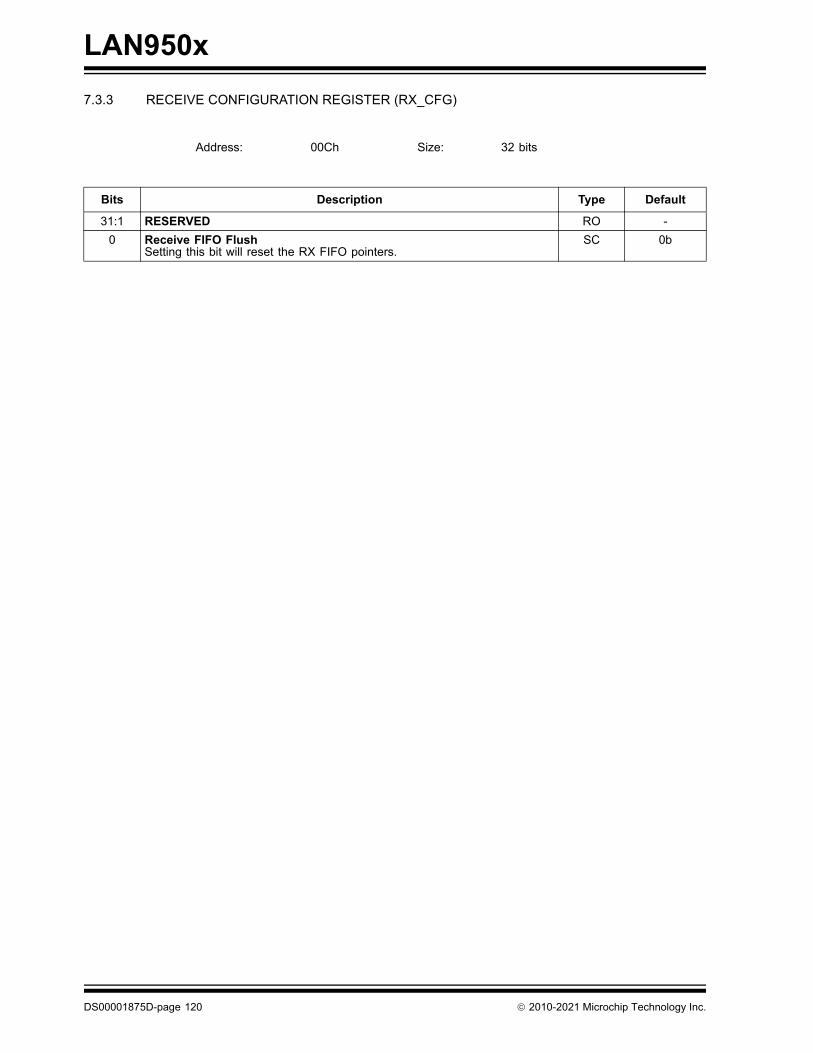
LAN950x
7.3.3 RECEIVE CONFIGURATION REGISTER (RX_CFG)
Address: 00Ch Size: 32 bits
Bits Description Type Default
31:1 RESERVED RO -
0 Receive FIFO FlushSetting this bit will reset the RX FIFO pointers.
SC 0b
DS00001875D-page 120 2010-2021 Microchip Technology Inc.
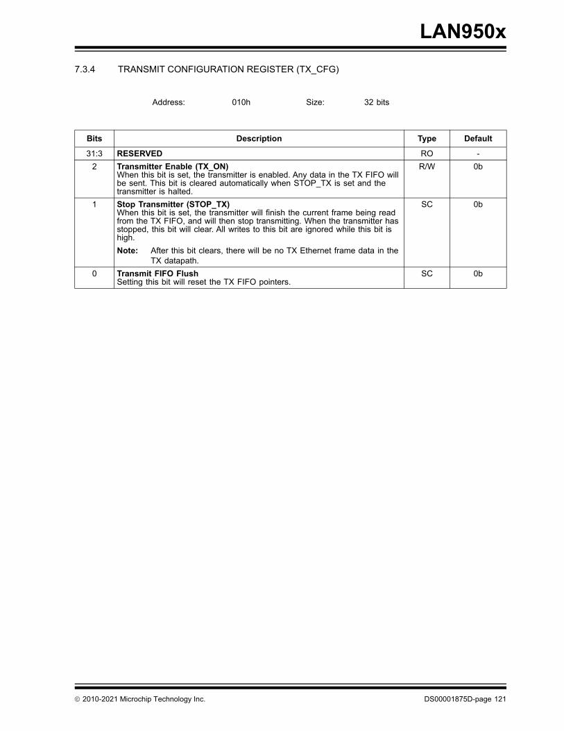
LAN950x
7.3.4 TRANSMIT CONFIGURATION REGISTER (TX_CFG)
Address: 010h Size: 32 bits
Bits Description Type Default
31:3 RESERVED RO -
2 Transmitter Enable (TX_ON)When this bit is set, the transmitter is enabled. Any data in the TX FIFO will be sent. This bit is cleared automatically when STOP_TX is set and the transmitter is halted.
R/W 0b
1 Stop Transmitter (STOP_TX)When this bit is set, the transmitter will finish the current frame being read from the TX FIFO, and will then stop transmitting. When the transmitter has stopped, this bit will clear. All writes to this bit are ignored while this bit is high.
Note: After this bit clears, there will be no TX Ethernet frame data in the TX datapath.
SC 0b
0 Transmit FIFO FlushSetting this bit will reset the TX FIFO pointers.
SC 0b
2010-2021 Microchip Technology Inc. DS00001875D-page 121

LAN950x
7.3.5 HARDWARE CONFIGURATION REGISTER (HW_CFG)
Address: 014h Size: 32 bits
Bits Description Type Default
31:19 RESERVED RO -
18 (LAN9500A/LAN9500Ai ONLY, Otherwise RESERVED)
NetDetach Status (SMDET_STS)After the driver loads, this bit is checked to determine whether an NetDetach event occurred.
R/WC Note 7-6
17 (LAN9500A/LAN9500Ai ONLY, Otherwise RESERVED)
NetDetach Enable (SMDET_EN)When this bit is set, the device detaches from the USB bus. This results in the driver unloading and no further communication with the device. The device remains detached until PHY link is detected, or a properly configured GPIO pin is asserted. Occurrence of either event causes the device to attach to the USB bus, the driver to be loaded, and the SMDET_STS bit to be asserted.
SC 0b
16 (LAN9500A/LAN9500Ai ONLY, Otherwise RESERVED)
EEPROM Emulation Enable (EEM)This bit is used to select the source of descriptor information and configuration flags when no EEPROM is present.
0 = Use defaults as specified in Section 5.7.2, "EEPROM Defaults," on page 82.
1 = Use Descriptor RAM and Attributes Registers
Note 1: This bit affects operation only when a EEPROM is not present. Thisbit has no effect when a EEPROM is present.
2: This field is protected by Reset Protection (RST_PROTECT).
R/W 0b
15 (LAN9500A/LAN9500Ai ONLY, Otherwise RESERVED)
Reset Protection (RST_PROTECT)Setting this bit protects select fields of certain registers from being affected by resets other than POR.
Note: This field is protected by Reset Protection (RST_PROTECT).
R/W 0b
14:13 (LAN9500A/LAN9500Ai ONLY, Otherwise RESERVED)
PHY Boost (PHY_BOOST)This field provides the ability to boost the electrical drive strength of the HS output current to the upstream port.
00 = Normal electrical drive strength01 = Elevated electrical drive strength (+4% boost)10 = Elevated electrical drive strength (+8% boost)11 = Elevated electrical drive strength (+12% boost)
Note: This field is protected by Reset Protection (RST_PROTECT).
R/W Note 7-7
12 Bulk In Empty Response (BIR)This bit controls the response to Bulk IN tokens when the RX FIFO is empty.
0 = Respond to the IN token with a ZLP1 = Respond to the IN token with a NAK
R/W 0b
11 Activity LED 80 ms Bypass (LEDB)When set, the Activity LED on/off time is reduced to approximately 15us/15us.
R/W 0b
DS00001875D-page 122 2010-2021 Microchip Technology Inc.
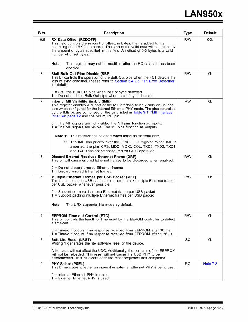
LAN950x
10:9 RX Data Offset (RXDOFF)This field controls the amount of offset, in bytes, that is added to the beginning of an RX Data packet. The start of the valid data will be shifted by the amount of bytes specified in this field. An offset of 0-3 bytes is a valid number of offset bytes.
Note: This register may not be modified after the RX datapath has been enabled.
R/W 00b
8 Stall Bulk Out Pipe Disable (SBP)This bit controls the operation of the Bulk Out pipe when the FCT detects the loss of sync condition. Please refer to Section 5.4.2.5, "TX Error Detection" for details.
0 = Stall the Bulk Out pipe when loss of sync detected.1 = Do not stall the Bulk Out pipe when loss of sync detected.
R/W 0b
7 Internal MII Visibility Enable (IME)This register enables a subset of the MII interface to be visible on unused pins when configured for the internal Ethernet PHY mode. The pins controlled by the IME bit are comprised of the pins listed in Table 3-1, “MII Interface Pins,” on page 12 and the nPHY_INT pin.
0 = The MII signals are not visible. The MII pins function as inputs.1 = The MII signals are visible. The MII pins function as outputs.
Note 1: This register has no affect when using an external PHY.
2: The IME has priority over the GPIO_CFG register. When IME isasserted, the pins CRS, MDC, MDIO, COL, TXD3, TXD2, TXD1,and TXD0 can not be configured for GPIO operation.
RW 0b
6 Discard Errored Received Ethernet Frame (DRP)This bit will cause errored Ethernet frames to be discarded when enabled.
0 = Do not discard errored Ethernet frames1 = Discard errored Ethernet frames.
R/W 0b
5 Multiple Ethernet Frames per USB Packet (MEF)This bit enables the USB transmit direction to pack multiple Ethernet frames per USB packet whenever possible.
0 = Support no more than one Ethernet frame per USB packet1 = Support packing multiple Ethernet frames per USB packet
Note: The URX supports this mode by default.
R/W 0b
4 EEPROM Time-out Control (ETC)This bit controls the length of time used by the EEPOM controller to detect a time-out.
0 = Time-out occurs if no response received from EEPROM after 30 ms.1 = Time-out occurs if no response received from EEPROM after 1.28 us.
R/W 0b
3 Soft Lite Reset (LRST)Writing 1 generates the lite software reset of the device.
A lite reset will not affect the UDC. Additionally, the contents of the EEPROM will not be reloaded. This reset will not cause the USB PHY to be disconnected. This bit clears after the reset sequence has completed.
SC 0b
2 PHY Select (PSEL)This bit indicates whether an internal or external Ethernet PHY is being used.
0 = Internal Ethernet PHY is used.1 = External Ethernet PHY is used.
RO Note 7-8
Bits Description Type Default
2010-2021 Microchip Technology Inc. DS00001875D-page 123
LAN950x
Note 7-6 The default value of this bit depends on whether a NetDetach event occurred. If set, the eventoccurred.
Note 7-7 The default value of this field is determined by the value of the PHY Boost field of the ConfigurationFlags contained within the EEPROM, if present. If no EEPROM is present, 00b is the default. A USBReset or Lite Reset (LRST) will cause this field to be restored to the image value last loaded fromEEPROM, or to be set to 00b if no EEPROM is present.
Note 7-8 The PHY_SEL pin determines the default value.
1 Burst Cap Enable (BCE)This register enables use of the burst cap register, Section 7.3.14, "Burst Cap Register (BURST_CAP)".
0 = Burst Cap register is not used to limit the TX burst size.1 = Burst Cap register is used to limit the TX burst size.
R/W 0b
0 Soft Reset (SRST)Writing 1 generates a software initiated reset of the device. If an external Ethernet PHY is used, it will be reset as well.
A software reset will result in the contents of the EEPROM being reloaded. While the reset sequence is in progress, the USB PHY will be disconnected. After the device has been reinitialized, it will take the PHY out of the disconnect state and be visible to the Host.
SC 0b
Bits Description Type Default
DS00001875D-page 124 2010-2021 Microchip Technology Inc.
LAN950x
7.3.6 RECEIVE FIFO INFORMATION REGISTER (RX_FIFO_INF)
Address: 018h Size: 32 bits
Bits Description Type Default
31:16 RESERVED RO -
15:0 RX Data FIFO Used Space (RXDUSED)Reads the amount of space in bytes used in the RX Data FIFO. For each receive frame, this field is incremented by the length of the receive data rounded up to the nearest DWORD (if the payload does not end on a DWORD boundary).
RO 0000h
2010-2021 Microchip Technology Inc. DS00001875D-page 125
LAN950x
7.3.7 TRANSMIT FIFO INFORMATION REGISTER (TX_FIFO_INF)
Address: 01Ch Size: 32 bits
Bits Description Type Default
31:16 RESERVED RO -
15:0 TX Data FIFO Free Space (TDFREE)Reads the amount of space, in bytes, available in the TX Data FIFO.
RO 2000h
DS00001875D-page 126 2010-2021 Microchip Technology Inc.
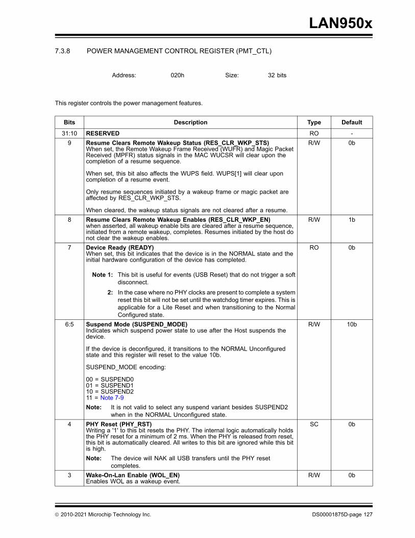
LAN950x
7.3.8 POWER MANAGEMENT CONTROL REGISTER (PMT_CTL)
This register controls the power management features.
Address: 020h Size: 32 bits
Bits Description Type Default
31:10 RESERVED RO -
9 Resume Clears Remote Wakeup Status (RES_CLR_WKP_STS)When set, the Remote Wakeup Frame Received (WUFR) and Magic Packet Received (MPFR) status signals in the MAC WUCSR will clear upon the completion of a resume sequence.
When set, this bit also affects the WUPS field. WUPS[1] will clear upon completion of a resume event.
Only resume sequences initiated by a wakeup frame or magic packet are affected by RES_CLR_WKP_STS.
When cleared, the wakeup status signals are not cleared after a resume.
R/W 0b
8 Resume Clears Remote Wakeup Enables (RES_CLR_WKP_EN)when asserted, all wakeup enable bits are cleared after a resume sequence, initiated from a remote wakeup, completes. Resumes initiated by the host do not clear the wakeup enables.
R/W 1b
7 Device Ready (READY)When set, this bit indicates that the device is in the NORMAL state and the initial hardware configuration of the device has completed.
Note 1: This bit is useful for events (USB Reset) that do not trigger a softdisconnect.
2: In the case where no PHY clocks are present to complete a systemreset this bit will not be set until the watchdog timer expires. This isapplicable for a Lite Reset and when transitioning to the NormalConfigured state.
RO 0b
6:5 Suspend Mode (SUSPEND_MODE)Indicates which suspend power state to use after the Host suspends the device.
If the device is deconfigured, it transitions to the NORMAL Unconfigured state and this register will reset to the value 10b.
SUSPEND_MODE encoding:
00 = SUSPEND001 = SUSPEND110 = SUSPEND211 = Note 7-9
Note: It is not valid to select any suspend variant besides SUSPEND2 when in the NORMAL Unconfigured state.
R/W 10b
4 PHY Reset (PHY_RST)Writing a '1' to this bit resets the PHY. The internal logic automatically holds the PHY reset for a minimum of 2 ms. When the PHY is released from reset, this bit is automatically cleared. All writes to this bit are ignored while this bit is high.
Note: The device will NAK all USB transfers until the PHY reset completes.
SC 0b
3 Wake-On-Lan Enable (WOL_EN)Enables WOL as a wakeup event.
R/W 0b
2010-2021 Microchip Technology Inc. DS00001875D-page 127
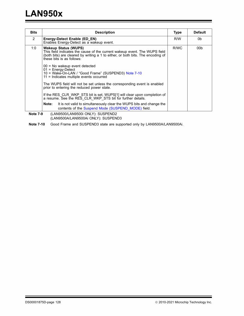
LAN950x
Note 7-9 (LAN9500/LAN9500i ONLY): SUSPEND2(LAN9500A/LAN9500Ai ONLY): SUSPEND3
Note 7-10 Good Frame and SUSPEND3 state are supported only by LAN9500A/LAN9500Ai.
2 Energy-Detect Enable (ED_EN)Enables Energy-Detect as a wakeup event.
R/W 0b
1:0 Wakeup Status (WUPS)This field indicates the cause of the current wakeup event. The WUPS field (both bits) are cleared by writing a 1 to either, or both bits. The encoding of these bits is as follows:
00 = No wakeup event detected01 = Energy-Detect10 = Wake-On-LAN / “Good Frame” (SUSPEND3) Note 7-1011 = Indicates multiple events occurred
The WUPS field will not be set unless the corresponding event is enabled prior to entering the reduced power state.
If the RES_CLR_WKP_STS bit is set, WUPS[1] will clear upon completion of a resume. See the RES_CLR_WKP_STS bit for further details.
Note: It is not valid to simultaneously clear the WUPS bits and change the contents of the Suspend Mode (SUSPEND_MODE) field.
R/WC 00b
Bits Description Type Default
DS00001875D-page 128 2010-2021 Microchip Technology Inc.
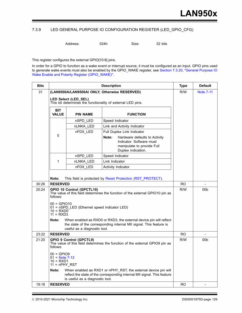
LAN950x
7.3.9 LED GENERAL PURPOSE IO CONFIGURATION REGISTER (LED_GPIO_CFG)
This register configures the external GPIO[10:8] pins.
In order for a GPIO to function as a wake event or interrupt source, it must be configured as an input. GPIO pins usedto generate wake events must also be enabled by the GPIO_WAKE register, see Section 7.3.20, "General Purpose IOWake Enable and Polarity Register (GPIO_WAKE)".
Address: 024h Size: 32 bits
Bits Description Type Default
31 (LAN9500A/LAN9500Ai ONLY, Otherwise RESERVED)
LED Select (LED_SEL)This bit determines the functionality of external LED pins.
Note: This field is protected by Reset Protection (RST_PROTECT).
R/W Note 7-11
30:26 RESERVED RO -
25:24 GPIO 10 Control (GPCTL10)The value of this field determines the function of the external GPIO10 pin as follows:
00 = GPIO1001 = nSPD_LED (Ethernet speed indicator LED)10 = RXD011 = RXD3
Note: When enabled as RXD0 or RXD3, the external device pin will reflect the state of the corresponding internal MII signal. This feature is useful as a diagnostic tool.
R/W 00b
23:22 RESERVED RO -
21:20 GPIO 9 Control (GPCTL9)The value of this field determines the function of the external GPIO9 pin as follows:
00 = GPIO901 = Note 7-12 10 = RXD111 = nPHY_RST
Note: When enabled as RXD1 or nPHY_RST, the external device pin will reflect the state of the corresponding internal MII signal. This feature is useful as a diagnostic tool.
R/W 00b
19:18 RESERVED RO -
BIT VALUE PIN NAME FUNCTION
0
nSPD_LED Speed Indicator
nLNKA_LED Link and Activity Indicator
nFDX_LED Full Duplex Link Indicator
Note: Hardware defaults to Activity Indicator. Software must manipulate to provide Full Duplex indication.
1
nSPD_LED Speed Indicator
nLNKA_LED Link Indicator
nFDX_LED Activity Indicator
2010-2021 Microchip Technology Inc. DS00001875D-page 129
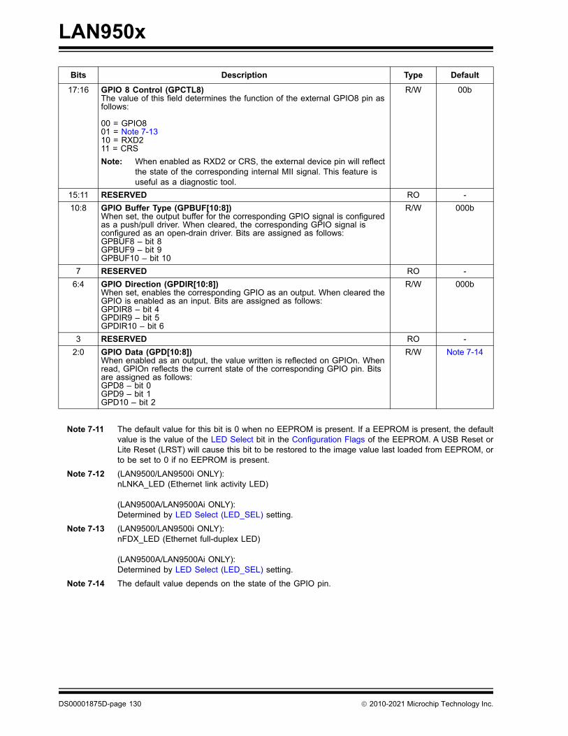
LAN950x
Note 7-11 The default value for this bit is 0 when no EEPROM is present. If a EEPROM is present, the defaultvalue is the value of the LED Select bit in the Configuration Flags of the EEPROM. A USB Reset orLite Reset (LRST) will cause this bit to be restored to the image value last loaded from EEPROM, orto be set to 0 if no EEPROM is present.
Note 7-12 (LAN9500/LAN9500i ONLY):nLNKA_LED (Ethernet link activity LED)
(LAN9500A/LAN9500Ai ONLY):Determined by LED Select (LED_SEL) setting.
Note 7-13 (LAN9500/LAN9500i ONLY):nFDX_LED (Ethernet full-duplex LED)
(LAN9500A/LAN9500Ai ONLY):Determined by LED Select (LED_SEL) setting.
Note 7-14 The default value depends on the state of the GPIO pin.
17:16 GPIO 8 Control (GPCTL8)The value of this field determines the function of the external GPIO8 pin as follows:
00 = GPIO801 = Note 7-1310 = RXD211 = CRS
Note: When enabled as RXD2 or CRS, the external device pin will reflect the state of the corresponding internal MII signal. This feature is useful as a diagnostic tool.
R/W 00b
15:11 RESERVED RO -
10:8 GPIO Buffer Type (GPBUF[10:8])When set, the output buffer for the corresponding GPIO signal is configured as a push/pull driver. When cleared, the corresponding GPIO signal is configured as an open-drain driver. Bits are assigned as follows:GPBUF8 – bit 8GPBUF9 – bit 9GPBUF10 – bit 10
R/W 000b
7 RESERVED RO -
6:4 GPIO Direction (GPDIR[10:8])When set, enables the corresponding GPIO as an output. When cleared the GPIO is enabled as an input. Bits are assigned as follows:GPDIR8 – bit 4GPDIR9 – bit 5GPDIR10 – bit 6
R/W 000b
3 RESERVED RO -
2:0 GPIO Data (GPD[10:8])When enabled as an output, the value written is reflected on GPIOn. When read, GPIOn reflects the current state of the corresponding GPIO pin. Bits are assigned as follows:GPD8 – bit 0GPD9 – bit 1GPD10 – bit 2
R/W Note 7-14
Bits Description Type Default
DS00001875D-page 130 2010-2021 Microchip Technology Inc.
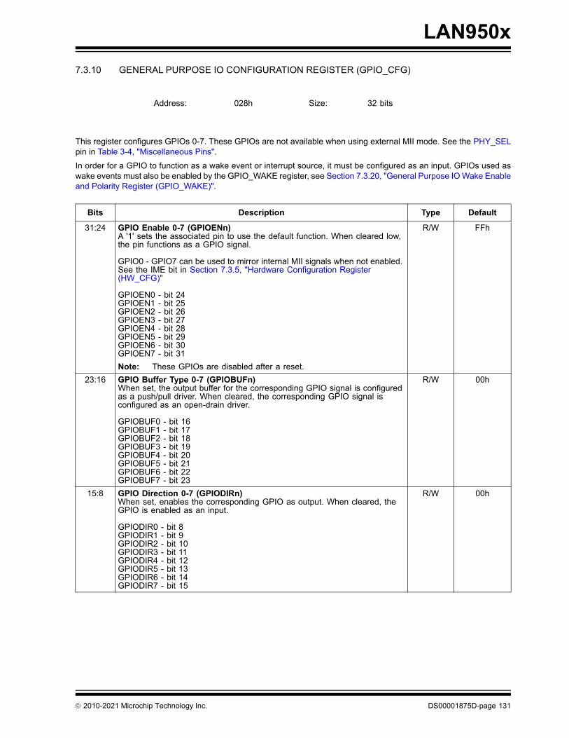
LAN950x
7.3.10 GENERAL PURPOSE IO CONFIGURATION REGISTER (GPIO_CFG)
This register configures GPIOs 0-7. These GPIOs are not available when using external MII mode. See the PHY_SELpin in Table 3-4, "Miscellaneous Pins".
In order for a GPIO to function as a wake event or interrupt source, it must be configured as an input. GPIOs used aswake events must also be enabled by the GPIO_WAKE register, see Section 7.3.20, "General Purpose IO Wake Enableand Polarity Register (GPIO_WAKE)".
Address: 028h Size: 32 bits
Bits Description Type Default
31:24 GPIO Enable 0-7 (GPIOENn)A '1' sets the associated pin to use the default function. When cleared low, the pin functions as a GPIO signal.
GPIO0 - GPIO7 can be used to mirror internal MII signals when not enabled. See the IME bit in Section 7.3.5, "Hardware Configuration Register (HW_CFG)"
GPIOEN0 - bit 24GPIOEN1 - bit 25GPIOEN2 - bit 26GPIOEN3 - bit 27GPIOEN4 - bit 28GPIOEN5 - bit 29GPIOEN6 - bit 30GPIOEN7 - bit 31
Note: These GPIOs are disabled after a reset.
R/W FFh
23:16 GPIO Buffer Type 0-7 (GPIOBUFn)When set, the output buffer for the corresponding GPIO signal is configured as a push/pull driver. When cleared, the corresponding GPIO signal is configured as an open-drain driver.
GPIOBUF0 - bit 16GPIOBUF1 - bit 17GPIOBUF2 - bit 18GPIOBUF3 - bit 19GPIOBUF4 - bit 20GPIOBUF5 - bit 21GPIOBUF6 - bit 22GPIOBUF7 - bit 23
R/W 00h
15:8 GPIO Direction 0-7 (GPIODIRn)When set, enables the corresponding GPIO as output. When cleared, the GPIO is enabled as an input.
GPIODIR0 - bit 8GPIODIR1 - bit 9GPIODIR2 - bit 10GPIODIR3 - bit 11GPIODIR4 - bit 12GPIODIR5 - bit 13GPIODIR6 - bit 14GPIODIR7 - bit 15
R/W 00h
2010-2021 Microchip Technology Inc. DS00001875D-page 131
LAN950x
Note 7-15 The default value depends on the state of the GPIO pin.
7:0 GPIO Data 0-7 (GPIODn)When enabled as an output, the value written is reflected on GPIOn. When read, GPIODn reflects the current state of the corresponding GPIO pin.
GPIOD0 - bit 0GPIOD1 - bit 1GPIOD2 - bit 2GPIOD3 - bit 3GPIOD4 - bit 4GPIOD5 - bit 5GPIOD6 - bit 6GPIOD7 - bit 7
R/W Note 7-15
Bits Description Type Default
DS00001875D-page 132 2010-2021 Microchip Technology Inc.
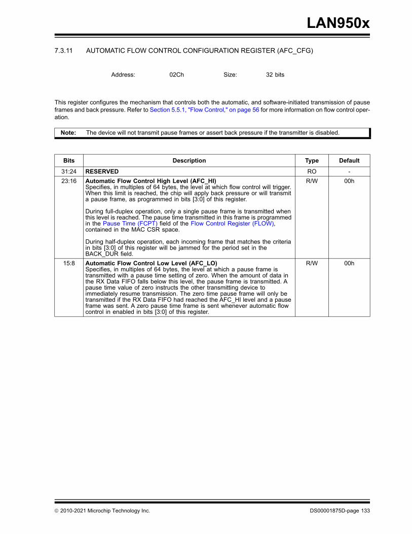
LAN950x
7.3.11 AUTOMATIC FLOW CONTROL CONFIGURATION REGISTER (AFC_CFG)
This register configures the mechanism that controls both the automatic, and software-initiated transmission of pauseframes and back pressure. Refer to Section 5.5.1, "Flow Control," on page 56 for more information on flow control oper-ation.
Address: 02Ch Size: 32 bits
Note: The device will not transmit pause frames or assert back pressure if the transmitter is disabled.
Bits Description Type Default
31:24 RESERVED RO -
23:16 Automatic Flow Control High Level (AFC_HI)Specifies, in multiples of 64 bytes, the level at which flow control will trigger. When this limit is reached, the chip will apply back pressure or will transmit a pause frame, as programmed in bits [3:0] of this register.
During full-duplex operation, only a single pause frame is transmitted when this level is reached. The pause time transmitted in this frame is programmed in the Pause Time (FCPT) field of the Flow Control Register (FLOW), contained in the MAC CSR space.
During half-duplex operation, each incoming frame that matches the criteria in bits [3:0] of this register will be jammed for the period set in the BACK_DUR field.
R/W 00h
15:8 Automatic Flow Control Low Level (AFC_LO)Specifies, in multiples of 64 bytes, the level at which a pause frame is transmitted with a pause time setting of zero. When the amount of data in the RX Data FIFO falls below this level, the pause frame is transmitted. A pause time value of zero instructs the other transmitting device to immediately resume transmission. The zero time pause frame will only be transmitted if the RX Data FIFO had reached the AFC_HI level and a pause frame was sent. A zero pause time frame is sent whenever automatic flow control in enabled in bits [3:0] of this register.
R/W 00h
2010-2021 Microchip Technology Inc. DS00001875D-page 133
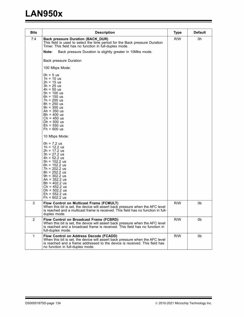
LAN950x
7:4 Back pressure Duration (BACK_DUR)This field is used to select the time period for the Back pressure Duration Timer. This field has no function in full-duplex mode.
Note: Back pressure Duration is slightly greater in 10Mbs mode.
Back pressure Duration
100 Mbps Mode:
0h = 5 us1h = 10 us2h = 15 us3h = 25 us4h = 50 us5h = 100 us6h = 150 us7h = 200 us8h = 250 us9h = 300 usAh = 350 usBh = 400 usCh = 450 usDh = 500 usEh = 550 usFh = 600 us
10 Mbps Mode:
0h = 7.2 us1h = 12.2 us2h = 17.2 us3h = 27.2 us4h = 52.2 us5h = 102.2 us6h = 152.2 us7h = 202.2 us8h = 252.2 us9h = 302.2 usAh = 352.2 usBh = 402.2 usCh = 452.2 usDh = 502.2 usEh = 552.2 usFh = 602.2 us
R/W 0h
3 Flow Control on Multicast Frame (FCMULT)When this bit is set, the device will assert back pressure when the AFC level is reached and a multicast frame is received. This field has no function in full-duplex mode.
R/W 0b
2 Flow Control on Broadcast Frame (FCBRD)When this bit is set, the device will assert back pressure when the AFC level is reached and a broadcast frame is received. This field has no function in full-duplex mode.
R/W 0b
1 Flow Control on Address Decode (FCADD)When this bit is set, the device will assert back pressure when the AFC level is reached and a frame addressed to the device is received. This field has no function in full-duplex mode.
R/W 0b
Bits Description Type Default
DS00001875D-page 134 2010-2021 Microchip Technology Inc.
LAN950x
0 Flow Control on Any Frame (FCANY)When this bit is set, the device will assert back pressure, or transmit a pause frame when the AFC level is reached and any frame is received. Setting this bit enables full-duplex flow control when the device is operating in full-duplex mode.
When this mode is enabled during half-duplex operation, the Flow Controller does not decode the MAC address and will send a pause frame upon receipt of a valid preamble (i.e., immediately at the beginning of the next frame after the RX Data FIFO level is reached).
When this mode is enabled during full-duplex operation, the Flow Controller will immediately instruct the MAC to send a pause frame when the RX Data FIFO level is reached. The MAC will queue the pause frame transmission for the next available window.
Setting this bit overrides bits [3:1] of this register.
R/W 0b
Bits Description Type Default
2010-2021 Microchip Technology Inc. DS00001875D-page 135
LAN950x
7.3.12 EEPROM COMMAND REGISTER (E2P_CMD)
This register is used to control the read and write operations on the Serial EEPROM.
Address: 030h Size: 32 bits
Bits Description Type Default
31 EPC BusyWhen a “1” is written into this bit, the operation specified in the EPC Command field is performed at the specified EEPROM address. This bit will remain set until the operation is complete. In the case of a read, this means that the Host can read valid data from the E2P Data register. The E2P_CMD and E2P_DATA registers should not be modified until this bit is cleared. In the case where a write is attempted and an EEPROM is not present, the EPC Busy remains busy until the EPC Time-out occurs. At that time, the busy bit is cleared.
Note: EPC busy will be high immediately following power-up, chip-level, or USB reset. After the EEPROM controller has finished reading (or attempting to read) the USB Descriptors and Ethernet default register values, the EPC Busy bit is cleared.
SC 0b
DS00001875D-page 136 2010-2021 Microchip Technology Inc.
LAN950x
30:28 EPC CommandThis field is used to issue commands to the EEPROM controller. The EPC will execute commands when the EPC Busy bit is set. A new command must not be issued until the previous command completes. This field is encoded as follows:
000 = READ001 = EWDS010 = EWEN011 = WRITE100 = WRAL101 = ERASE110 = ERAL111 = RELOAD
READ (Read Location): This command will cause a read of the EEPROM location pointed to by EPC Address. The result of the read is available in the E2P_DATA register.
EWDS (Erase/Write Disable): After issued, the EEPROM will ignore erase and write commands. To re-enable erase/write operations, issue the EWEN command.
EWEN (Erase/Write Enable): Enables the EEPROM for erase and write operations. The EEPROM will allow erase and write operations until the Erase/Write Disable command is sent, or until power is cycled.
Note: The EEPROM device will power-up in the erase/write-disabled state. Any erase or write operations will fail until an Erase/Write Enable command is issued.
WRITE (Write Location): If erase/write operations are enabled in the EEPROM, this command will cause the contents of the E2P_DATA register to be written to the EEPROM location selected by the EPC Address field.
WRAL (Write All): If erase/write operations are enabled in the EEPROM, this command will cause the contents of the E2P_DATA register to be written to every EEPROM memory location.
ERASE (Erase Location): If erase/write operations are enabled in the EEPROM, this command will erase the location selected by the EPC Address field.
ERAL (Erase All): If erase/write operations are enabled in the EEPROM, this command will initiate a bulk erase of the entire EEPROM.
RELOAD (Data Reload): Instructs the EEPROM controller to reload the data from the EEPROM. If a value of A5h is not found in the first address of the EEPROM, the EEPROM is assumed to be un-programmed and the Reload operation will fail. The “Data Loaded” bit indicates a successful load of the data.
Note: A failed reload operation will result in no change to descriptor information or register contents. These items will not be set to default values as a result of the reload failure.
R/W 000b
27:11 RESERVED RO -
Bits Description Type Default
2010-2021 Microchip Technology Inc. DS00001875D-page 137
LAN950x
10 EPC Time-outIf an EEPROM operation is performed, and there is no response from the EEPROM within 30mS, the EEPROM controller will time-out and return to its idle state. This bit is set when a time-out occurs, indicating that the last operation was unsuccessful.
Note: If the EEDI pin is pulled-high (default if left unconnected), EPC commands will not time out if the EEPROM device is missing. In this case, the EPC Busy bit will be cleared as soon as the command sequence is complete. It should also be noted that the ERASE, ERAL, WRITE and WRAL commands are the only EPC commands that will time-out if an EEPROM device is not present and the EEDI signal is pulled low.
R/WC 0
9 Data LoadedWhen set, this bit indicates that a valid EEPROM was found, and that the USB and Ethernet Data programming has completed normally. This bit is set after a successful load of the data after power-up, or after a RELOAD command has completed.
R/WC 0
8:0 EPC AddressThe 9-bit value in this field is used by the EEPROM Controller to address a specific memory location in the Serial EEPROM. This is a BYTE aligned address.
R/W 00h
Bits Description Type Default
DS00001875D-page 138 2010-2021 Microchip Technology Inc.
LAN950x
7.3.13 EEPROM DATA REGISTER (E2P_DATA)
This register is used in conjunction with the E2P_CMD register to perform read and write operations to the SerialEEPROM.
Address: 034h Size: 32 bits
Bits Description Type Default
31:8 RESERVED RO -
7:0 EEPROM DataValue read from or written to the EEPROM.
R/W 00h
2010-2021 Microchip Technology Inc. DS00001875D-page 139
LAN950x
7.3.14 BURST CAP REGISTER (BURST_CAP)
This register is used to limit the size of the data burst transmitted by the UTX. When more than the amount specified inthe BURST_CAP register is transmitted, the UTX will send a ZLP.
Address: 038h Size: 32 bits
Note: This register must be enabled through the Section 7.3.5, "Hardware Configuration Register (HW_CFG)".
Bits Description Type Default
31:8 RESERVED RO -
7:0 BURST_CAPThe maximum amount of contiguous data that may be transmitted by the UTX before a ZLP is sent. This field has units of 512 bytes for HS mode and 64 bytes for FS mode.
Note: A value less than or equal to 4 in HS mode or less than or equal to 32 in FS mode indicates that burst cap enforcement is disabled. In this case, the UTX always responds to In Tokens with a ZLP when the Bulk In Empty Response (BIR) bit in the Hardware Configuration Register (HW_CFG) is deasserted. It will respond with NAKs if the Bulk In Empty Response (BIR) bit is set.
R/W 00h
DS00001875D-page 140 2010-2021 Microchip Technology Inc.
LAN950x
7.3.15 DATA PORT SELECT REGISTER (DP_SEL)
Before accessing the internal RAMs, the TESTEN bit must be set. It is not valid to use the RAM data port during run time.
The RAM Test Mode Select chooses which internal RAM to access.
The Data Port Ready bit indicates when the data port RAM access has completed. In the case of a read operation, thisindicates when the read data has been stored in the DP_DATA register.
Address: 040h Size: 32 bits
Bits Description Type Default
31 Data Port Ready (DPRDY)
0 = data port is busy processing a transaction1 = data port is ready
RO 1b
30:3 RESERVED RO -
2:1 RAM Test Select (RSEL)Selects which RAM to access.
00 = FCT Data RAM01 = EEPROM storage RAM10 = TX TLI RAM11 = RX TLI RAM
R/W 0b
0 RAM Test Mode Enable (TESTEN)Put all test accessible RAMs in test mode.
R/W 0b
2010-2021 Microchip Technology Inc. DS00001875D-page 141
LAN950x
7.3.16 DATA PORT COMMAND REGISTER (DP_CMD)
This register commences the data port access. Writing a one to this register will enable a write access, while writing azero will do a read access.
The address and data registers need to be configured appropriately for the desired read or write operation beforeaccessing this register.
Address: 044h Size: 32 bits
Bits Description Type Default
31:1 RESERVED RO -
0 Data Port Write.Selects operation. Writing to this bit initiates the data port access.
0 = read operation1 = write operation
R/W 0b
DS00001875D-page 142 2010-2021 Microchip Technology Inc.
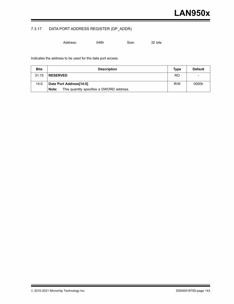
LAN950x
7.3.17 DATA PORT ADDRESS REGISTER (DP_ADDR)
Indicates the address to be used for the data port access.
Address: 048h Size: 32 bits
Bits Description Type Default
31:15 RESERVED RO -
14:0 Data Port Address[14:0]
Note: This quantity specifies a DWORD address.
R/W 0000h
2010-2021 Microchip Technology Inc. DS00001875D-page 143
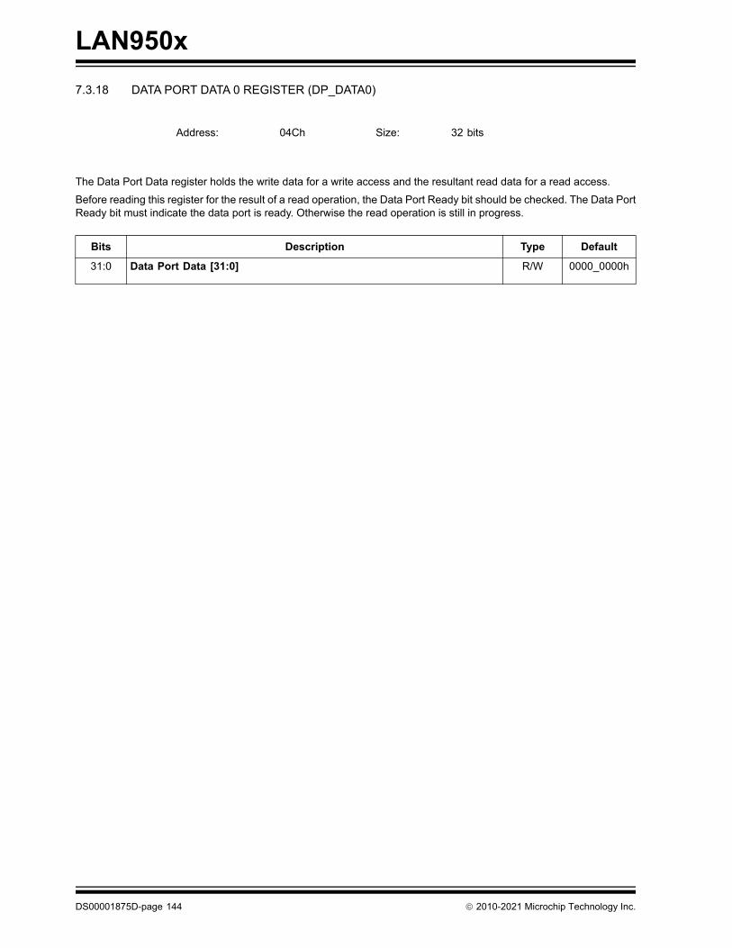
LAN950x
7.3.18 DATA PORT DATA 0 REGISTER (DP_DATA0)
The Data Port Data register holds the write data for a write access and the resultant read data for a read access.
Before reading this register for the result of a read operation, the Data Port Ready bit should be checked. The Data PortReady bit must indicate the data port is ready. Otherwise the read operation is still in progress.
Address: 04Ch Size: 32 bits
Bits Description Type Default
31:0 Data Port Data [31:0] R/W 0000_0000h
DS00001875D-page 144 2010-2021 Microchip Technology Inc.
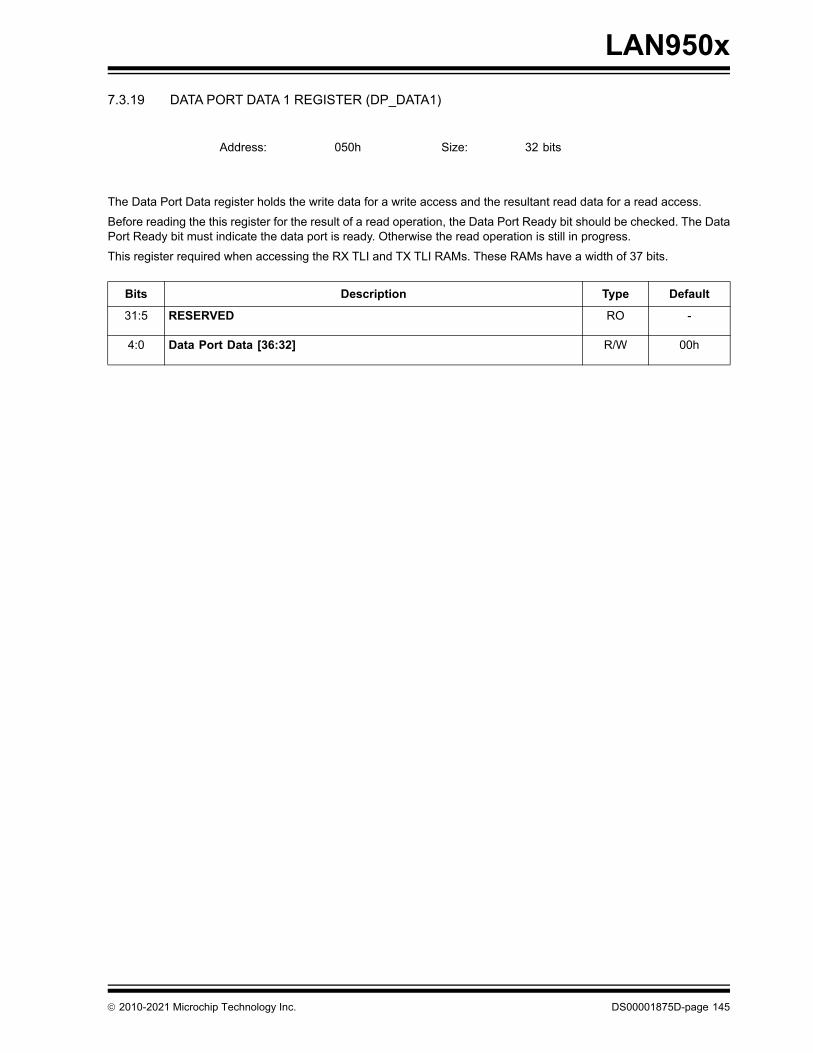
LAN950x
7.3.19 DATA PORT DATA 1 REGISTER (DP_DATA1)
The Data Port Data register holds the write data for a write access and the resultant read data for a read access.
Before reading the this register for the result of a read operation, the Data Port Ready bit should be checked. The DataPort Ready bit must indicate the data port is ready. Otherwise the read operation is still in progress.
This register required when accessing the RX TLI and TX TLI RAMs. These RAMs have a width of 37 bits.
Address: 050h Size: 32 bits
Bits Description Type Default
31:5 RESERVED RO -
4:0 Data Port Data [36:32] R/W 00h
2010-2021 Microchip Technology Inc. DS00001875D-page 145
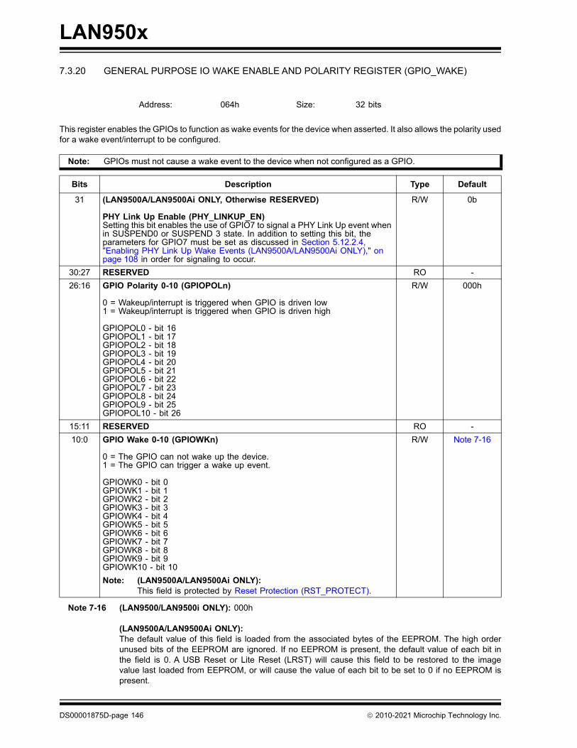
LAN950x
7.3.20 GENERAL PURPOSE IO WAKE ENABLE AND POLARITY REGISTER (GPIO_WAKE)
This register enables the GPIOs to function as wake events for the device when asserted. It also allows the polarity usedfor a wake event/interrupt to be configured.
Note 7-16 (LAN9500/LAN9500i ONLY): 000h
(LAN9500A/LAN9500Ai ONLY):The default value of this field is loaded from the associated bytes of the EEPROM. The high orderunused bits of the EEPROM are ignored. If no EEPROM is present, the default value of each bit inthe field is 0. A USB Reset or Lite Reset (LRST) will cause this field to be restored to the imagevalue last loaded from EEPROM, or will cause the value of each bit to be set to 0 if no EEPROM ispresent.
Address: 064h Size: 32 bits
Note: GPIOs must not cause a wake event to the device when not configured as a GPIO.
Bits Description Type Default
31 (LAN9500A/LAN9500Ai ONLY, Otherwise RESERVED)
PHY Link Up Enable (PHY_LINKUP_EN)Setting this bit enables the use of GPIO7 to signal a PHY Link Up event when in SUSPEND0 or SUSPEND 3 state. In addition to setting this bit, the parameters for GPIO7 must be set as discussed in Section 5.12.2.4, "Enabling PHY Link Up Wake Events (LAN9500A/LAN9500Ai ONLY)," on page 108 in order for signaling to occur.
R/W 0b
30:27 RESERVED RO -
26:16 GPIO Polarity 0-10 (GPIOPOLn)
0 = Wakeup/interrupt is triggered when GPIO is driven low1 = Wakeup/interrupt is triggered when GPIO is driven high
GPIOPOL0 - bit 16GPIOPOL1 - bit 17GPIOPOL2 - bit 18GPIOPOL3 - bit 19GPIOPOL4 - bit 20GPIOPOL5 - bit 21GPIOPOL6 - bit 22GPIOPOL7 - bit 23GPIOPOL8 - bit 24GPIOPOL9 - bit 25GPIOPOL10 - bit 26
R/W 000h
15:11 RESERVED RO -
10:0 GPIO Wake 0-10 (GPIOWKn)
0 = The GPIO can not wake up the device.1 = The GPIO can trigger a wake up event.
GPIOWK0 - bit 0GPIOWK1 - bit 1GPIOWK2 - bit 2GPIOWK3 - bit 3GPIOWK4 - bit 4GPIOWK5 - bit 5GPIOWK6 - bit 6GPIOWK7 - bit 7GPIOWK8 - bit 8GPIOWK9 - bit 9GPIOWK10 - bit 10
Note: (LAN9500A/LAN9500Ai ONLY):This field is protected by Reset Protection (RST_PROTECT).
R/W Note 7-16
DS00001875D-page 146 2010-2021 Microchip Technology Inc.
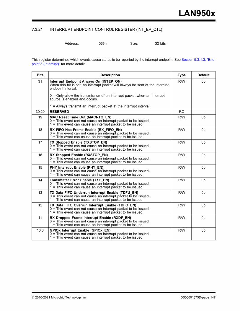
LAN950x
7.3.21 INTERRUPT ENDPOINT CONTROL REGISTER (INT_EP_CTL)
This register determines which events cause status to be reported by the interrupt endpoint. See Section 5.3.1.3, "End-point 3 (Interrupt)" for more details.
Address: 068h Size: 32 bits
Bits Description Type Default
31 Interrupt Endpoint Always On (INTEP_ON)When this bit is set, an interrupt packet will always be sent at the interrupt endpoint interval.
0 = Only allow the transmission of an interrupt packet when an interrupt source is enabled and occurs.
1 = Always transmit an interrupt packet at the interrupt interval.
R/W 0b
30:20 RESERVED RO -
19 MAC Reset Time Out (MACRTO_EN)0 = This event can not cause an interrupt packet to be issued.1 = This event can cause an interrupt packet to be issued.
R/W 0b
18 RX FIFO Has Frame Enable (RX_FIFO_EN)0 = This event can not cause an interrupt packet to be issued.1 = This event can cause an interrupt packet to be issued.
R/W 0b
17 TX Stopped Enable (TXSTOP_EN)0 = This event can not cause an interrupt packet to be issued.1 = This event can cause an interrupt packet to be issued.
R/W 0b
16 RX Stopped Enable (RXSTOP_EN) 0 = This event can not cause an interrupt packet to be issued.1 = This event can cause an interrupt packet to be issued.
R/W 0b
15 PHY Interrupt Enable (PHY_EN)0 = This event can not cause an interrupt packet to be issued.1 = This event can cause an interrupt packet to be issued.
R/W 0b
14 Transmitter Error Enable (TXE_EN)0 = This event can not cause an interrupt packet to be issued.1 = This event can cause an interrupt packet to be issued.
R/W 0b
13 TX Data FIFO Underrun Interrupt Enable (TDFU_EN)0 = This event can not cause an interrupt packet to be issued.1 = This event can cause an interrupt packet to be issued.
R/W 0b
12 TX Data FIFO Overrun Interrupt Enable (TDFO_EN)0 = This event can not cause an interrupt packet to be issued.1 = This event can cause an interrupt packet to be issued.
R/W 0b
11 RX Dropped Frame Interrupt Enable (RXDF_EN) 0 = This event can not cause an interrupt packet to be issued.1 = This event can cause an interrupt packet to be issued.
R/W 0b
10:0 GPIOx Interrupt Enable (GPIOx_EN)0 = This event can not cause an interrupt packet to be issued.1 = This event can cause an interrupt packet to be issued.
R/W 0b
2010-2021 Microchip Technology Inc. DS00001875D-page 147
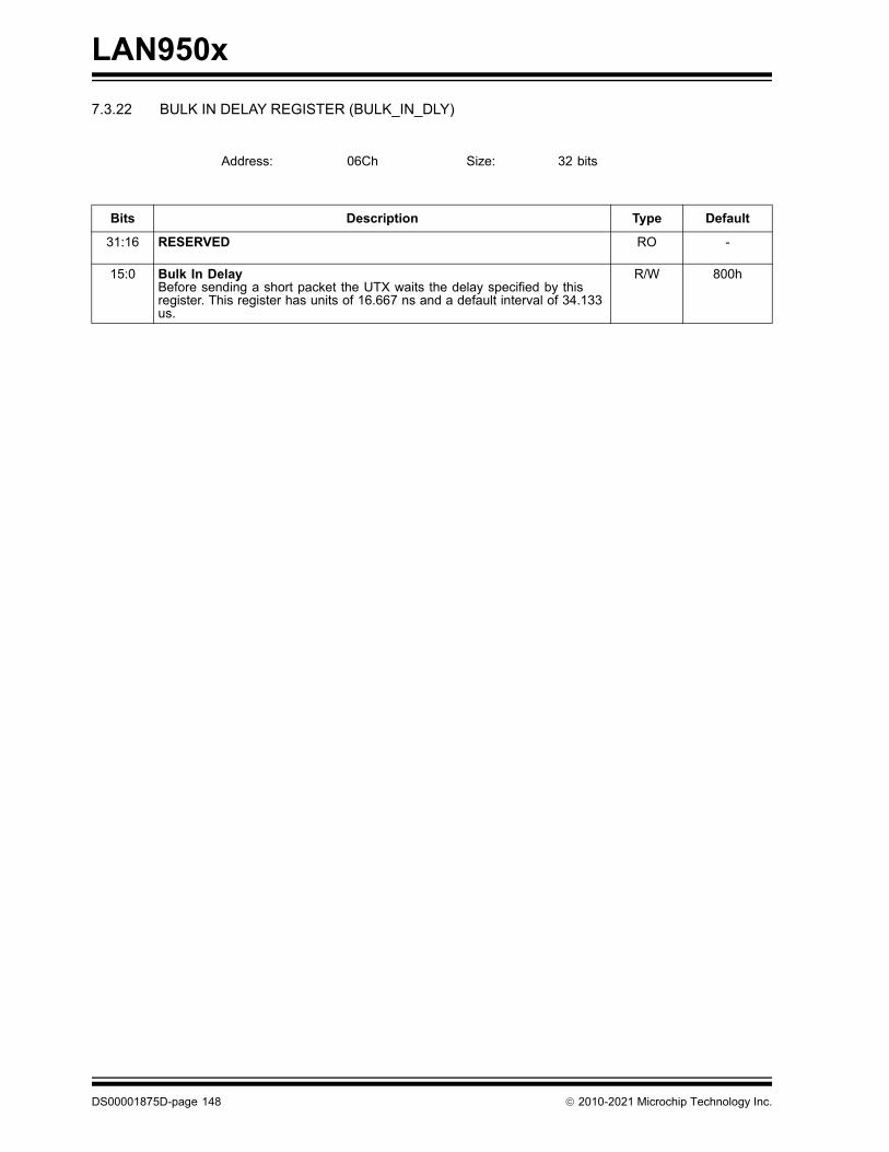
LAN950x
7.3.22 BULK IN DELAY REGISTER (BULK_IN_DLY)
Address: 06Ch Size: 32 bits
Bits Description Type Default
31:16 RESERVED RO -
15:0 Bulk In DelayBefore sending a short packet the UTX waits the delay specified by this register. This register has units of 16.667 ns and a default interval of 34.133 us.
R/W 800h
DS00001875D-page 148 2010-2021 Microchip Technology Inc.
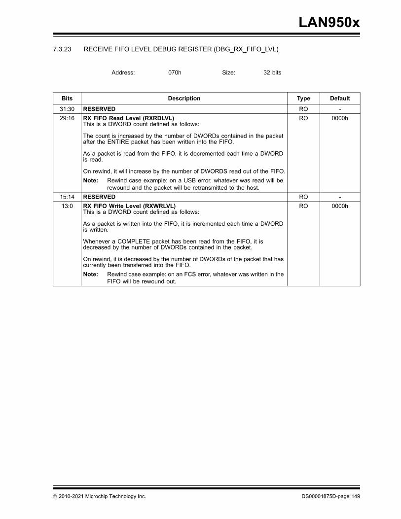
LAN950x
7.3.23 RECEIVE FIFO LEVEL DEBUG REGISTER (DBG_RX_FIFO_LVL)
Address: 070h Size: 32 bits
Bits Description Type Default
31:30 RESERVED RO -
29:16 RX FIFO Read Level (RXRDLVL)This is a DWORD count defined as follows:
The count is increased by the number of DWORDs contained in the packet after the ENTIRE packet has been written into the FIFO.
As a packet is read from the FIFO, it is decremented each time a DWORD is read.
On rewind, it will increase by the number of DWORDS read out of the FIFO.
Note: Rewind case example: on a USB error, whatever was read will be rewound and the packet will be retransmitted to the host.
RO 0000h
15:14 RESERVED RO -
13:0 RX FIFO Write Level (RXWRLVL)This is a DWORD count defined as follows:
As a packet is written into the FIFO, it is incremented each time a DWORD is written.
Whenever a COMPLETE packet has been read from the FIFO, it is decreased by the number of DWORDs contained in the packet.
On rewind, it is decreased by the number of DWORDs of the packet that has currently been transferred into the FIFO.
Note: Rewind case example: on an FCS error, whatever was written in the FIFO will be rewound out.
RO 0000h
2010-2021 Microchip Technology Inc. DS00001875D-page 149
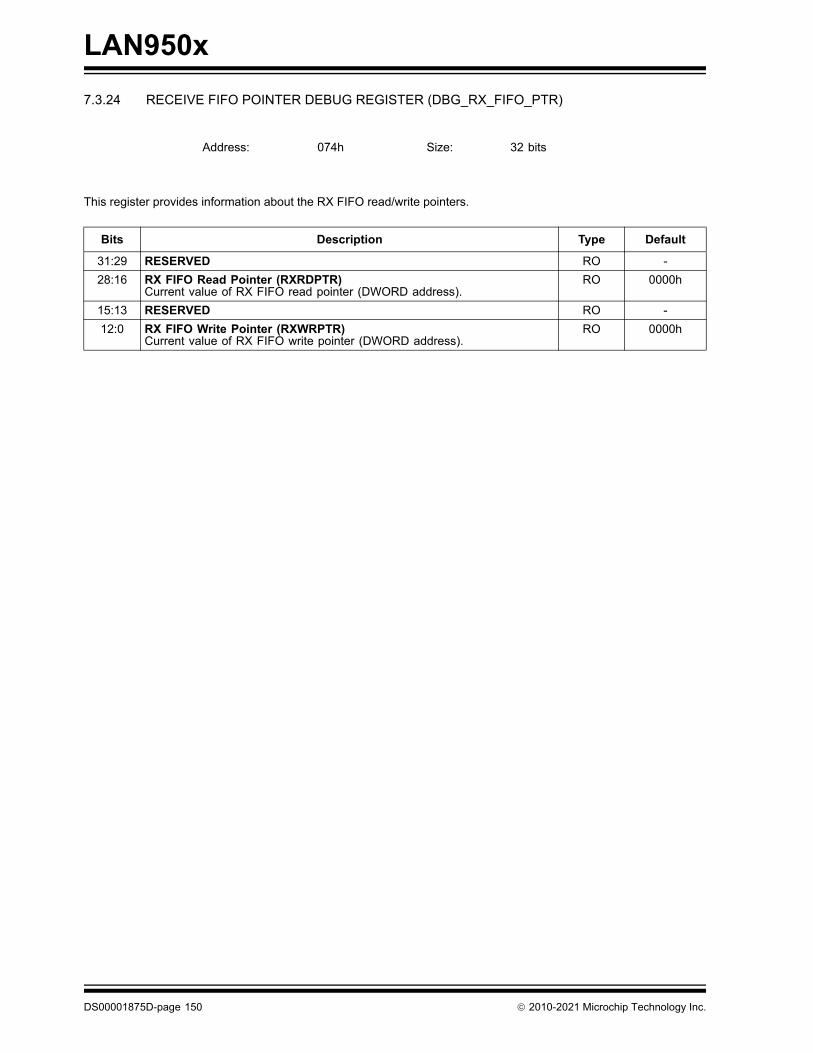
LAN950x
7.3.24 RECEIVE FIFO POINTER DEBUG REGISTER (DBG_RX_FIFO_PTR)
This register provides information about the RX FIFO read/write pointers.
Address: 074h Size: 32 bits
Bits Description Type Default
31:29 RESERVED RO -
28:16 RX FIFO Read Pointer (RXRDPTR)Current value of RX FIFO read pointer (DWORD address).
RO 0000h
15:13 RESERVED RO -
12:0 RX FIFO Write Pointer (RXWRPTR)Current value of RX FIFO write pointer (DWORD address).
RO 0000h
DS00001875D-page 150 2010-2021 Microchip Technology Inc.
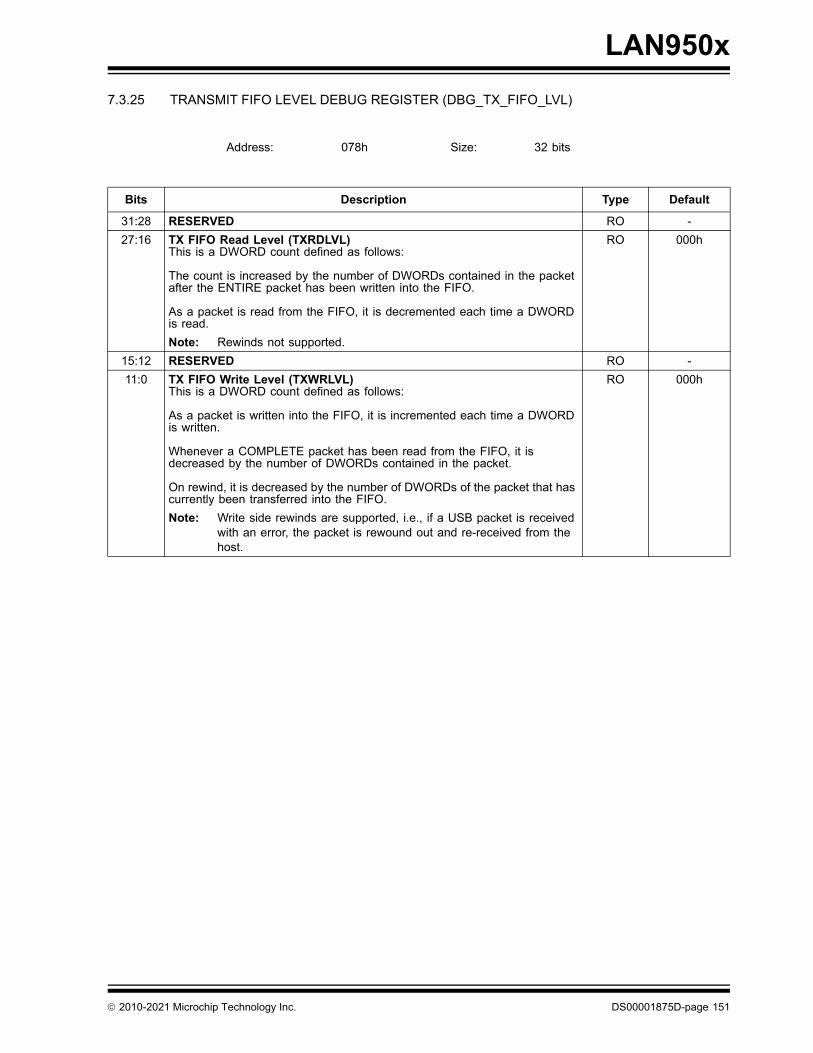
LAN950x
7.3.25 TRANSMIT FIFO LEVEL DEBUG REGISTER (DBG_TX_FIFO_LVL)
Address: 078h Size: 32 bits
Bits Description Type Default
31:28 RESERVED RO -
27:16 TX FIFO Read Level (TXRDLVL)This is a DWORD count defined as follows:
The count is increased by the number of DWORDs contained in the packet after the ENTIRE packet has been written into the FIFO.
As a packet is read from the FIFO, it is decremented each time a DWORD is read.
Note: Rewinds not supported.
RO 000h
15:12 RESERVED RO -
11:0 TX FIFO Write Level (TXWRLVL)This is a DWORD count defined as follows:
As a packet is written into the FIFO, it is incremented each time a DWORD is written.
Whenever a COMPLETE packet has been read from the FIFO, it is decreased by the number of DWORDs contained in the packet.
On rewind, it is decreased by the number of DWORDs of the packet that has currently been transferred into the FIFO.
Note: Write side rewinds are supported, i.e., if a USB packet is received with an error, the packet is rewound out and re-received from the host.
RO 000h
2010-2021 Microchip Technology Inc. DS00001875D-page 151

LAN950x
7.3.26 TRANSMIT FIFO POINTER DEBUG REGISTER (DBG_TX_FIFO_PTR)
This register provides information about the TX FIFO read/write pointers.
Address: 07Ch Size: 32 bits
Bits Description Type Default
31:27 RESERVED RO -
26:16 TX FIFO Read Pointer (TXRDPTR)Current value of TX FIFO read pointer (DWORD address).
RO 000h
15:11 RESERVED RO -
10:0 TX FIFO Write Pointer (TXWRPTR)Current value of TX FIFO write pointer (DWORD address).
RO 000h
DS00001875D-page 152 2010-2021 Microchip Technology Inc.
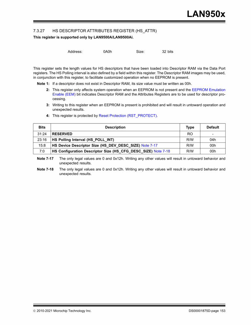
LAN950x
7.3.27 HS DESCRIPTOR ATTRIBUTES REGISTER (HS_ATTR)
This register is supported only by LAN9500A/LAN9500Ai.
This register sets the length values for HS descriptors that have been loaded into Descriptor RAM via the Data Portregisters. The HS Polling interval is also defined by a field within this register. The Descriptor RAM images may be used,in conjunction with this register, to facilitate customized operation when no EEPROM is present.
Note 1: If a descriptor does not exist in Descriptor RAM, its size value must be written as 00h.
2: This register only affects system operation when an EEPROM is not present and the EEPROM EmulationEnable (EEM) bit indicates Descriptor RAM and the Attributes Registers are to be used for descriptor pro-cessing.
3: Writing to this register when an EEPROM is present is prohibited and will result in untoward operation andunexpected results.
4: This register is protected by Reset Protection (RST_PROTECT).
Note 7-17 The only legal values are 0 and 0x12h. Writing any other values will result in untoward behavior andunexpected results.
Note 7-18 The only legal values are 0 and 0x12h. Writing any other values will result in untoward behavior andunexpected results.
Address: 0A0h Size: 32 bits
Bits Description Type Default
31:24 RESERVED RO -
23:16 HS Polling Interval (HS_POLL_INT) R/W 04h
15:8 HS Device Descriptor Size (HS_DEV_DESC_SIZE) Note 7-17 R/W 00h
7:0 HS Configuration Descriptor Size (HS_CFG_DESC_SIZE) Note 7-18 R/W 00h
2010-2021 Microchip Technology Inc. DS00001875D-page 153
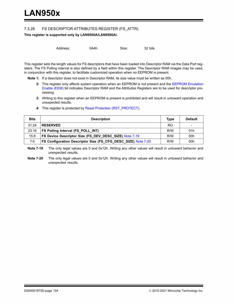
LAN950x
7.3.28 FS DESCRIPTOR ATTRIBUTES REGISTER (FS_ATTR)
This register is supported only by LAN9500A/LAN9500Ai.
This register sets the length values for FS descriptors that have been loaded into Descriptor RAM via the Data Port reg-isters. The FS Polling interval is also defined by a field within this register. The Descriptor RAM images may be used,in conjunction with this register, to facilitate customized operation when no EEPROM is present.
Note 1: If a descriptor does not exist in Descriptor RAM, its size value must be written as 00h.
2: This register only affects system operation when an EEPROM is not present and the EEPROM EmulationEnable (EEM) bit indicates Descriptor RAM and the Attributes Registers are to be used for descriptor pro-cessing.
3: Writing to this register when an EEPROM is present is prohibited and will result in untoward operation andunexpected results.
4: This register is protected by Reset Protection (RST_PROTECT).
Note 7-19 The only legal values are 0 and 0x12h. Writing any other values will result in untoward behavior andunexpected results.
Note 7-20 The only legal values are 0 and 0x12h. Writing any other values will result in untoward behavior andunexpected results.
Address: 0A4h Size: 32 bits
Bits Description Type Default
31:24 RESERVED RO -
23:16 FS Polling Interval (FS_POLL_INT) R/W 01h
15:8 FS Device Descriptor Size (FS_DEV_DESC_SIZE) Note 7-19 R/W 00h
7:0 FS Configuration Descriptor Size (FS_CFG_DESC_SIZE) Note 7-20 R/W 00h
DS00001875D-page 154 2010-2021 Microchip Technology Inc.
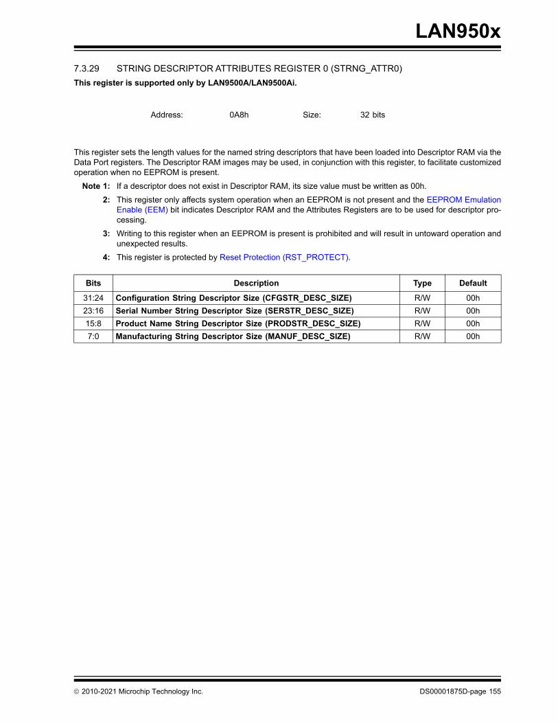
LAN950x
7.3.29 STRING DESCRIPTOR ATTRIBUTES REGISTER 0 (STRNG_ATTR0)
This register is supported only by LAN9500A/LAN9500Ai.
This register sets the length values for the named string descriptors that have been loaded into Descriptor RAM via theData Port registers. The Descriptor RAM images may be used, in conjunction with this register, to facilitate customizedoperation when no EEPROM is present.
Note 1: If a descriptor does not exist in Descriptor RAM, its size value must be written as 00h.
2: This register only affects system operation when an EEPROM is not present and the EEPROM EmulationEnable (EEM) bit indicates Descriptor RAM and the Attributes Registers are to be used for descriptor pro-cessing.
3: Writing to this register when an EEPROM is present is prohibited and will result in untoward operation andunexpected results.
4: This register is protected by Reset Protection (RST_PROTECT).
Address: 0A8h Size: 32 bits
Bits Description Type Default
31:24 Configuration String Descriptor Size (CFGSTR_DESC_SIZE) R/W 00h
23:16 Serial Number String Descriptor Size (SERSTR_DESC_SIZE) R/W 00h
15:8 Product Name String Descriptor Size (PRODSTR_DESC_SIZE) R/W 00h
7:0 Manufacturing String Descriptor Size (MANUF_DESC_SIZE) R/W 00h
2010-2021 Microchip Technology Inc. DS00001875D-page 155
LAN950x
7.3.30 STRING DESCRIPTOR ATTRIBUTES REGISTER 1 (STRNG_ATTR1)
This register is supported only by LAN9500A/LAN9500Ai.
This register sets the length values for the named string descriptors that have been loaded into Descriptor RAM via theData Port registers. The Descriptor RAM images may be used, in conjunction with this register, to facilitate customizedoperation when no EEPROM is present.
Note 1: If a descriptor does not exist in Descriptor RAM, its size value must be written as 00h.
2: This register only affects system operation when an EEPROM is not present and the EEPROM EmulationEnable (EEM) bit indicates Descriptor RAM and the Attributes Registers are to be used for descriptor pro-cessing.
3: Writing to this register when an EEPROM is present is prohibited and will result in untoward operation andunexpected results.
4: This register is protected by Reset Protection (RST_PROTECT).
Address: 0ACh Size: 32 bits
Bits Description Type Default
31:8 RESERVED RO -
7:0 Interface String Descriptor Size (INTSTR_DESC_SIZE) R/W 00h
DS00001875D-page 156 2010-2021 Microchip Technology Inc.
LAN950x
7.3.31 FLAG ATTRIBUTES REGISTER (FLAG_ATTR)
This register is supported only by LAN9500A/LAN9500Ai.
This register sets the values of elements of the Configuration Flags and PME flags when no EEPROM is present andcustomized operation, using Descriptor RAM images, is to occur. This register does not contain Configuration Flag ele-ments that are components of other registers. Those elements will be programmed by the driver software directly priorto initiating customized operation via Descriptor RAM.
Note 1: This register only affects system operation when an EEPROM is not present and the EEPROM EmulationEnable (EEM) bit indicates Descriptor RAM and the Attributes Registers are to be used for descriptor pro-cessing.
2: Writing to this register when an EEPROM is present is prohibited and will result in untoward operation andunexpected results.
3: This register is protected by Reset Protection (RST_PROTECT).
Note 7-21 The default value depends on the setting of the RMT_WKP strap.
Note 7-22 The default value depends on the setting of the PWR_SEL strap.
Address: 0B0h Size: 32 bits
Bits Description Type Default
31:18 RESERVED RO -
17 Remote Wakeup Support (RMT_WKP)Refer to Remote Wakeup Support bit in Table 5-58, “Configuration Flags,” on page 80 for definition.
R/W Note 7-21
16 Power Method (PWR_SEL)Refer to Power Method bit in Table 5-58, “Configuration Flags,” on page 80 for definition.
R/W Note 7-22
15:8 RESERVED RO -
7:0 GPIO PME Flags (PME_FLAGS)Refer to Table 5-59, “GPIO PME Flags,” on page 81 for bit definitions.
R/W 00h
2010-2021 Microchip Technology Inc. DS00001875D-page 157
LAN950x
7.4 MAC Control and Status Registers
Table 7-4 lists the registers contained in this section.
TABLE 7-4: MAC CONTROL AND STATUS REGISTER (MCSR) MAP
Address Symbol Register Name
100h MAC_CR MAC Control Register
104h ADDRH MAC Address High Register
108h ADDRL MAC Address Low Register
10Ch HASHH Multicast Hash Table High Register
110h HASHL Multicast Hash Table Low Register
114h MII_ACCESS MII Access Register
118h MII_DATA MII Data Register
11Ch FLOW Flow Control Register
120h VLAN1 VLAN1 Tag Register
124h VLAN2 VLAN2 Tag Register
128h WUFF Wakeup Frame Filter Register
12Ch WUCSR Wakeup Control and Status Register
130h COE_CR Checksum Offload Engine Control Register
134h - 1FCh RESERVED Reserved for future use
DS00001875D-page 158 2010-2021 Microchip Technology Inc.
LAN950x
7.4.1 MAC CONTROL REGISTER (MAC_CR)
This register establishes the RX and TX operating modes and includes controls for address filtering and packet filtering..
Address: 100h Size: 32 bits
Bits Description Type Default
31 Receive All Mode (RXALL)When set, all incoming packets will be received and passed on to the address filtering function for processing of the selected filtering mode on the received frame. Address filtering then occurs and is reported in Receive Status. When reset, only frames that pass Destination Address filtering will be sent to the Application.
R/W 0b
30-24 RESERVED RO -
23 Disable Receive Own (RCVOWN)When set, the MAC disables the reception of frames when TXEN is asserted. The MAC blocks the transmitted frame on the receive path. When reset, the MAC receives all packets the PHY gives, including those transmitted by the MAC.This bit should be reset when the Full Duplex Mode bit is set.
R/W 0b
22 RESERVED RO -
21 Loopback Operation Mode (LOOPBK)Selects the loop back operation modes for the MAC. This is only for full duplex mode0 = Normal. No feedback1 = Internal through MIIIn internal loopback mode, the TX frame is received by the Internal MII interface, and sent back to the MAC without being sent to the PHY.
Note: When enabling or disabling the loopback mode, it can take up to 10s for the mode change to occur. The transmitter and receiver must be stopped and disabled when modifying the LOOPBK bit. The transmitter or receiver should not be enabled within10s of modifying the LOOPBK bit.
R/W 0b
20 Full Duplex Mode (FDPX)When set, the MAC operates in Full-Duplex mode, in which it can transmit and receive simultaneously.
R/W 0b
19 Pass All Multicast (MCPAS)When set, indicates that all incoming frames with a Multicast destination address (first bit in the destination address field is 1) are received. Incoming frames with physical address (Individual Address/Unicast) destinations are filtered and received only if the address matches the MAC Address.
R/W 0b
18 Promiscuous Mode (PRMS)When set, indicates that any incoming frame is received regardless of its destination address.
R/W 1b
17 Inverse filtering (INVFILT)When set, the address check Function operates in Inverse filtering mode. This is valid only during Perfect filtering mode.
R/W 0b
16 Pass Bad Frames (PASSBAD)When set, all incoming frames that passed address filtering are received, including runt frames, collided frames or truncated frames caused by buffer underrun.
R/W 0b
15 Hash Only Filtering mode (HO)When set, the address check Function operates in the imperfect address filtering mode both for physical and multicast addresses.
R/W 0b
14 RESERVED RO -
2010-2021 Microchip Technology Inc. DS00001875D-page 159
LAN950x
13 Hash/Perfect Filtering Mode (HPFILT)When reset (0), the device will implement a perfect address filter on incoming frames, according the address specified in the MAC address register.
When set (1), the address check function does imperfect address filtering of multicast incoming frames according to the hash table specified in the multicast hash table register.If the Hash Only Filtering mode (HO) bit is set (1), then the physical (IA) are imperfect filtered too. If the Hash Only Filtering mode (HO) bit is reset (0), then the IA addresses are perfect address filtered according to the MAC Address register
R/W 0b
12 Late Collision Control (LCOLL)When set, enables retransmission of the collided frame even after the collision period (late collision). When reset, the MAC disables frame transmission on a late collision. In any case, the Late Collision status is appropriately updated in the Transmit Packet status.
R/W 0b
11 Disable Broadcast Frames (BCAST)When set, disables the reception of broadcast frames. When reset, forwards all broadcast frames to the application.
Note: When wakeup frame detection is enabled via the Wakeup Frame Enable (WUEN) bit of the Wakeup Control and Status Register (WUCSR), a broadcast wakeup frame will wake up the device despite the state of this bit.
R/W 0b
10 Disable Retry (DISRTY)When set, the MAC attempts only one transmission. When a collision is seen on the bus, the MAC ignores the current frame and goes to the next frame and a retry error is reported in the Transmit status. When reset, the MAC attempts 16 transmissions before signaling a retry error.
R/W 0b
9 RESERVED RO -
8 Automatic Pad Stripping (PADSTR)When set, the MAC strips the pad field on all incoming frames, if the length field is less than 46 bytes. The FCS field is also stripped, since it is computed at the transmitting station based on the data and pad field characters, and is invalid for a received frame that has had the pad characters stripped. Receive frames with a 46-byte or greater length field are passed to the Application unmodified (FCS is not stripped). When reset, the MAC passes all incoming frames to system memory unmodified.
R/W 0b
Bits Description Type Default
DS00001875D-page 160 2010-2021 Microchip Technology Inc.
LAN950x
7:6 BackOff Limit (BOLMT)The BOLMT bits allow the user to set its back-off limit in a relaxed or aggressive mode. According to IEEE 802.3, the MAC has to wait for a random number [r] of slot-times (Note 7-23) after it detects a collision, where:(eq.1)0 < r < 2KThe exponent K is dependent on how many times the current frame to be transmitted has been retried, as follows: (eq.2)K = min (n, 10) where n is the current number of retries. If a frame has been retried three times, then K = 3 and r= 8 slot-times maximum. If it has been retried 12 times, then K = 10, and r = 1024 slot-times maximum.An LFSR (linear feedback shift register) 20-bit counter emulates a 20bit random number generator, from which r is obtained. Once a collision is detected, the number of the current retry of the current frame is used to obtain K (eq.2). This value of K translates into the number of bits to use from the LFSR counter. If the value of K is 3, the MAC takes the value in the first three bits of the LFSR counter and uses it to count down to zero on every slot-time. This effectively causes the MAC to wait eight slot-times. To give the user more flexibility, the BOLMT value forces the number of bits to be used from the LFSR counter to a predetermined value as in the table below.
Thus, if the value of K = 10, the MAC will look at the BOLMT if it is 00, then use the lower ten bits of the LFSR counter for the wait countdown. If the BOLMT is 10, then it will only use the value in the first four bits for the wait countdown, etc.
Note 7-23 Slot-time = 512 bit times. (See IEEE 802.3 Spec., Secs.4.2.3.25 and 4.4.2.1)
R/W 00b
5 Deferral Check (DFCHK)When set, enables the deferral check in the MAC. The MAC will abort the transmission attempt if it has deferred for more than 24,288 bit times. Deferral starts when the transmitter is ready to transmit, but is prevented from doing so because the CRS is active. Defer time is not cumulative. If the transmitter defers for 10,000 bit times, then transmits, collides, backs off, and then has to defer again after completion of back-off, the deferral timer resets to 0 and restarts. When reset, the deferral check is disabled in the MAC and the MAC defers indefinitely.
R/W 0b
4 RESERVED RO -
3 Transmitter Enable (TXEN)When set, the MAC’s transmitter is enabled and it will transmit frames from the buffer onto the cable. When reset, the MAC’s transmitter is disabled and will not transmit any frames.
R/W 0b
2 Receiver Enable (RXEN)When set (1), the MAC’s receiver is enabled and will receive frames from the internal PHY. When reset, the MAC’s receiver is disabled and will not receive any frames from the internal PHY.
R/W 0b
1:0 RESERVED RO -
Bits Description Type Default
BOLMT Value # Bits Used from LFSR Counter
00 10
01 8
10 4
11 1
2010-2021 Microchip Technology Inc. DS00001875D-page 161
LAN950x
7.4.2 MAC ADDRESS HIGH REGISTER (ADDRH)
This register contains the upper 16 bits of the physical address of the MAC, where ADDRH[15:8] is the 6th octet of theRX frame.
Address: 104h Size: 32 bits
Note: (LAN9500A/LAN9500Ai ONLY):This register is protected by Reset Protection (RST_PROTECT).
Bits Description Type Default
31:16 RESERVED RO -
15:0 Physical Address [47:32]This field contains the upper 16 bits (47:32) of the physical address of the device.
R/W FFFFh
DS00001875D-page 162 2010-2021 Microchip Technology Inc.
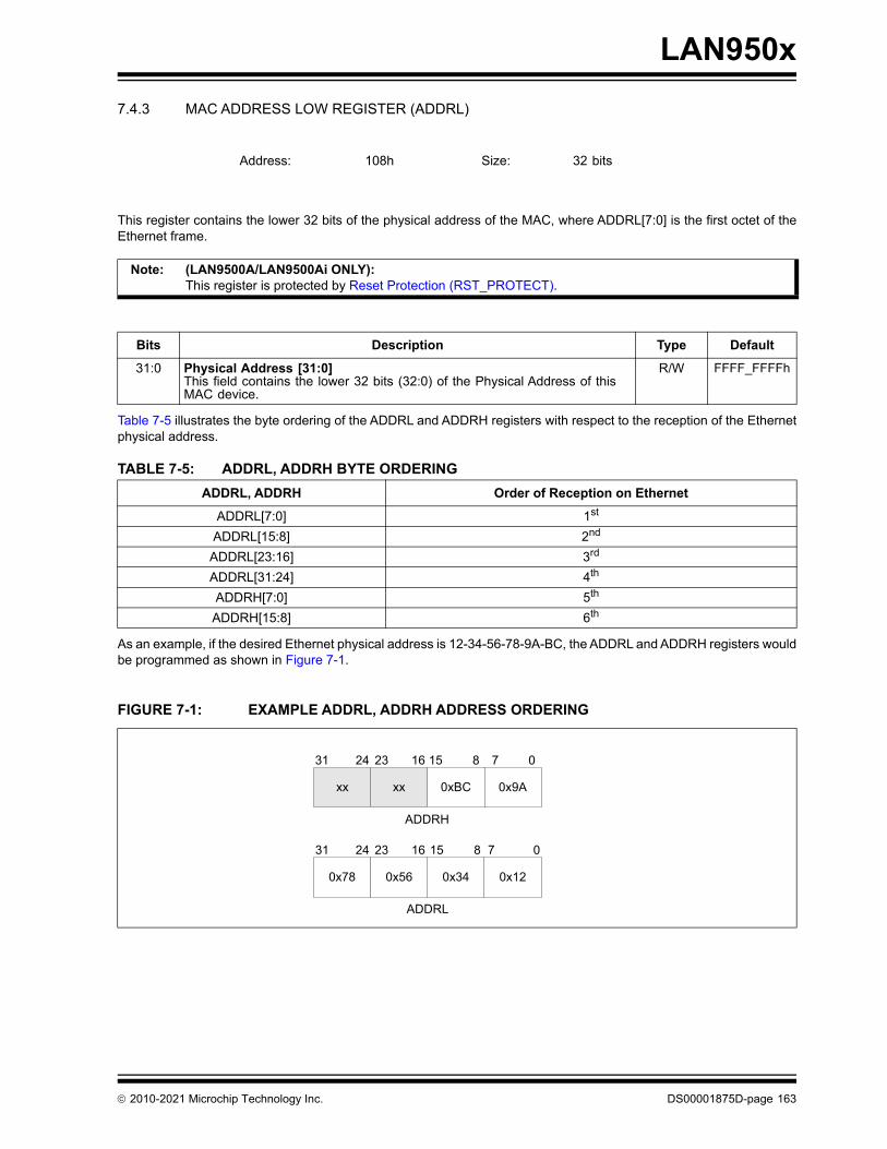
LAN950x
7.4.3 MAC ADDRESS LOW REGISTER (ADDRL)
This register contains the lower 32 bits of the physical address of the MAC, where ADDRL[7:0] is the first octet of theEthernet frame.
Table 7-5 illustrates the byte ordering of the ADDRL and ADDRH registers with respect to the reception of the Ethernetphysical address.
As an example, if the desired Ethernet physical address is 12-34-56-78-9A-BC, the ADDRL and ADDRH registers wouldbe programmed as shown in Figure 7-1.
Address: 108h Size: 32 bits
Note: (LAN9500A/LAN9500Ai ONLY):This register is protected by Reset Protection (RST_PROTECT).
Bits Description Type Default
31:0 Physical Address [31:0]This field contains the lower 32 bits (32:0) of the Physical Address of this MAC device.
R/W FFFF_FFFFh
TABLE 7-5: ADDRL, ADDRH BYTE ORDERING
ADDRL, ADDRH Order of Reception on Ethernet
ADDRL[7:0] 1st
ADDRL[15:8] 2nd
ADDRL[23:16] 3rd
ADDRL[31:24] 4th
ADDRH[7:0] 5th
ADDRH[15:8] 6th
FIGURE 7-1: EXAMPLE ADDRL, ADDRH ADDRESS ORDERING
0x12
07
0x34
815
0x56
1623
0x78
2431
ADDRL
0x9A
07
0xBC
815
ADDRH
xx
1623
xx
2431
2010-2021 Microchip Technology Inc. DS00001875D-page 163
LAN950x
7.4.4 MULTICAST HASH TABLE HIGH REGISTER (HASHH)
The 64-bit Multicast table is used for group address filtering. For hash filtering, the contents of the destination addressin the incoming frame is used to index the contents of the Hash table. The most significant bit determines the registerto be used (Hi/Low), while the other five bits determine the bit within the register. A value of 00000 selects Bit 0 of theMulticast Hash Table Lo register and a value of 11111 selects the Bit 31 of the Multicast Hash Table Hi register.
If the corresponding bit is 1, then the multicast frame is accepted. Otherwise, it is rejected. If the “Pass All Multicast” (MCPAS)bit is set (1), then all multicast frames are accepted regardless of the multicast hash values.
The Multicast Hash Table Hi register contains the higher 32 bits of the hash table and the Multicast Hash Table Lowregister contains the lower 32 bits of the hash table.
Address: 10Ch Size: 32 bits
Bits Description Type Default
31:0 Upper 32 bits of the 64-bit Hash Table R/W 0000_0000h
DS00001875D-page 164 2010-2021 Microchip Technology Inc.
LAN950x
7.4.5 MULTICAST HASH TABLE LOW REGISTER (HASHL)
This register defines the lower 32-bits of the Multicast Hash Table. Please refer to Section 7.4.4, "Multicast Hash TableHigh Register (HASHH)," on page 164 for further details.
Address: 110h Size: 32 bits
Bits Description Type Default
31:0 Lower 32 bits of the 64-bit Hash Table R/W 0000_0000h
2010-2021 Microchip Technology Inc. DS00001875D-page 165
LAN950x
7.4.6 MII ACCESS REGISTER (MII_ACCESS)
This register is used to control the management cycles to the internal PHY.
Address: 114h Size: 32 bits
Bits Description Type Default
31:16 RESERVED RO -
15:11 PHY AddressFor every access to this register, this field must be set to 00001b.
R/W 00000b
10:6 MII Register Index (MIIRINDA)These bits select the desired MII register in the PHY.
R/W 00000b
5:2 RESERVED RO -
1 MII Write (MIIWnR)Setting this bit tells the PHY that this will be a write operation using the MII data register. If this bit is not set, this will be a read operation, packing the data in the MII data register.
R/W 0b
0 MII Busy (MIIBZY)This bit must be polled to determine when the MII register access is complete. This bit must read a logical 0 before writing to this register or to the MII data register. The LAN driver software must set (1) this bit in order for the Host to read or write any of the MII PHY registers.
During a MII register access, this bit will be set, signifying a read or write access is in progress. The MII data register must be kept valid until the MAC clears this bit during a PHY write operation. The MII data register is invalid until the MAC has cleared this bit during a PHY read operation.
SC 0b
DS00001875D-page 166 2010-2021 Microchip Technology Inc.
LAN950x
7.4.7 MII DATA REGISTER (MII_DATA)
This register contains either the data to be written to the PHY register specified in the MII Access Register, or the readdata from the PHY register whose index is specified in the MII Access Register. Refer toSection 7.4.6, "MII Access Reg-ister (MII_ACCESS)," on page 166 for further details.
Address: 118h Size: 32 bits
Note: The MIIBZY bit in the MII_ACCESS register must be cleared when writing to this register.
Bits Description Type Default
31:16 RESERVED RO -
15:0 MII DataThis contains the 16-bit value read from the PHY read operation or the 16-bit data value to be written to the PHY before an MII write operation.
R/W 0000h
2010-2021 Microchip Technology Inc. DS00001875D-page 167
LAN950x
7.4.8 FLOW CONTROL REGISTER (FLOW)
This register is used to control the generation and reception of the Control frames by the MAC’s flow control block. Awrite to this register with busy bit set to 1 will trigger the Flow control block to generate a Control frame. Before writingto this register, the application has to make sure that the busy bit is not set.
Address: 11Ch Size: 32 bits
Bits Description Type Default
31:16 Pause Time (FCPT)This field indicates the value to be used in the PAUSE TIME field in the control frame.
R/W 0000h
15:3 RESERVED RO -
2 Pass Control Frames (FCPASS)When set, the MAC sets the packet filter bit in the receive packet status to indicate to the application that a valid pause frame has been received. The application must accept or discard a received frame based on the packet filter control bit. The MAC receives, decodes and performs the pause function when a valid pause frame is received in full-duplex mode and when flow control is enabled (FCEN bit set). When reset, the MAC resets the packet filter bit in the receive packet status.
The MAC always passes the data of all frames it receives (including flow control frames) to the application. Frames that do not pass address filtering, as well as frames with errors, are passed to the application. The application must discard or retain the received frame’s data based on the received frame’s STATUS field. Filtering modes (promiscuous mode, for example) take precedence over the FCPASS bit.
R/W 0b
1 Flow Control Enable (FCEN)When set, enables the MAC flow control function. The MAC decodes all incoming frames for control frames; if it receives a valid control frame (PAUSE command), it disables the transmitter for a specified time (Decoded pause time x slot time). When reset, the MAC flow control function is disabled; the MAC does not decode frames for control frames.
Note: Flow Control is applicable when the MAC is set in full duplex mode. In half-duplex mode, this bit enables the back pressure function to control the flow of received frames to the MAC.
R/W 0b
0 Flow Control Busy (FCBSY)This bit is set high whenever a pause frame or back pressure is being transmitted. This bit should read logical 0 before writing to the Flow Control (FLOW) register. During a transfer of Control Frame, this bit continues to be set, signifying that a frame transmission is in progress. After the PAUSE control frame's transmission is complete, the MAC resets to 0.
Note 1: When writing this register the FCBSY bit must always be zero.
2: Applications must always write a zero to this bit.
R/W 0b
DS00001875D-page 168 2010-2021 Microchip Technology Inc.
LAN950x
7.4.9 VLAN1 TAG REGISTER (VLAN1)
This register contains the VLAN tag field to identify VLAN1 frames. For VLAN frames, the legal frame length is increasedfrom 1518 bytes to 1522 bytes.
The RXCOE also uses this register to determine the protocol value to use to indicate the existence of a VLAN tag. Whenusing the RXCOE, this value may only be changed if the RX path is disabled. If it is desired to change this value duringrun time, it is safe to do so only after the MAC is disabled and the TLI is empty.
Address: 120h Size: 32 bits
Bits Description Type Default
31:16 RESERVED RO -
15:0 VLAN1 Tag Identifier (VTI1)This contains the VLAN Tag field to identify the VLAN1 frames. This field is compared with the 13th and 14th bytes of the incoming frames for VLAN1 frame detection.
R/W FFFFh
2010-2021 Microchip Technology Inc. DS00001875D-page 169
LAN950x
7.4.10 VLAN2 TAG REGISTER (VLAN2)
This register contains the VLAN tag field to identify VLAN2 frames. For VLAN frames the legal frame length is increasedfrom 1518 bytes to 1522 bytes.
Address: 124h Size: 32 bits
Bits Description Type Default
31:16 RESERVED RO -
15:0 VLAN2 Tag Identifier (VTI2)This contains the VLAN Tag field to identify the VLAN2 frames. This field is compared with the 13th and 14th bytes of the incoming frames for VLAN2 frame detection.
R/W FFFFh
DS00001875D-page 170 2010-2021 Microchip Technology Inc.
LAN950x
7.4.11 WAKEUP FRAME FILTER (WUFF)
This register is used to configure the Wakeup Frame Filter.
Note 7-24 The number of DWORD read/writes is dependent on the number of wakeup frames supported by thedevice. DWORD read/writes required are as follow:(LAN9500/LAN9500i ONLY): 20 (4 filters supported)(LAN9500A/LAN9500Ai ONLY): 40 (8 filters supported)
Address: 128h Size: 32 bits
Bits Description Type Default
31:0 Wakeup Frame Filter (WFF)The Wakeup Frame Filter is configured through this register using an indexing mechanism. Following a reset, the MAC loads the first value written to this location to the first DWORD in the Wakeup Frame Filter (Filter 0 Byte Mask 0). The second value written to this location is loaded to the second DWORD in the Wakeup Frame Filter (Filter 0 Byte Mask 1) and so on. Once the device dependent number of DWORDs have been written (Note 7-24), the internal pointer will once again point to the first entry and the filter entries can be modified in the same manner. Similarly, the device dependent number of DWORDS can be read sequentially to obtain the values stored in the WFF(Note 7-24). Please refer to Section 5.5.5, "Wakeup Frame Detection," on page 59 for further information concerning the Wakeup Frame Filter.
Note: This register should be read and written using the device dependent number of consecutive DWORD operations (Note 7-24). Failure to read or write the entire contents of the WFF may cause the internal read/write pointers to be left in a position other than pointing to the first entry. A mechanism for resetting the internal pointers to the beginning of the WFF is available via the WFF Pointer Reset (WFF_PTR_RST) bit of the Wakeup Control and Status Register (WUCSR). This mechanism enables the application program to re-synchronize with the internal WFF pointers if it has not previously read/written the complete contents of the WFF.
R/W 0000_0000h
2010-2021 Microchip Technology Inc. DS00001875D-page 171
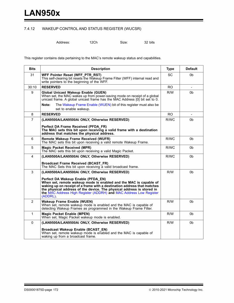
LAN950x
7.4.12 WAKEUP CONTROL AND STATUS REGISTER (WUCSR)
This register contains data pertaining to the MAC’s remote wakeup status and capabilities.
Address: 12Ch Size: 32 bits
Bits Description Type Default
31 WFF Pointer Reset (WFF_PTR_RST)This self-clearing bit resets the Wakeup Frame Filter (WFF) internal read and write pointers to the beginning of the WFF.
SC 0b
30:10 RESERVED RO -
9 Global Unicast Wakeup Enable (GUEN)When set, the MAC wakes up from power-saving mode on receipt of a global unicast frame. A global unicast frame has the MAC Address [0] bit set to 0.
Note: The Wakeup Frame Enable (WUEN) bit of this register must also be set to enable wakeup.
R/W 0b
8 RESERVED RO -
7 (LAN9500A/LAN9500Ai ONLY, Otherwise RESERVED)
Perfect DA Frame Received (PFDA_FR)The MAC sets this bit upon receiving a valid frame with a destination address that matches the physical address.
R/WC 0b
6 Remote Wakeup Frame Received (WUFR)The MAC sets this bit upon receiving a valid remote Wakeup Frame.
R/WC 0b
5 Magic Packet Received (MPR)The MAC sets this bit upon receiving a valid Magic Packet.
R/WC 0b
4 (LAN9500A/LAN9500Ai ONLY, Otherwise RESERVED)
Broadcast Frame Received (BCAST_FR)The MAC Sets this bit upon receiving a valid broadcast frame.
R/WC 0b
3 (LAN9500A/LAN9500Ai ONLY, Otherwise RESERVED)
Perfect DA Wakeup Enable (PFDA_EN)When set, remote wakeup mode is enabled and the MAC is capable of waking up on receipt of a frame with a destination address that matches the physical address of the device. The physical address is stored in the MAC Address High Register (ADDRH) and MAC Address Low Register (ADDRL).
R/W 0b
2 Wakeup Frame Enable (WUEN)When set, remote wakeup mode is enabled and the MAC is capable of detecting Wakeup Frames as programmed in the Wakeup Frame Filter.
R/W 0b
1 Magic Packet Enable (MPEN)When set, Magic Packet wakeup mode is enabled.
R/W 0b
0 (LAN9500A/LAN9500Ai ONLY, Otherwise RESERVED)
Broadcast Wakeup Enable (BCAST_EN)When set, remote wakeup mode is enabled and the MAC is capable of waking up from a broadcast frame.
R/W 0b
DS00001875D-page 172 2010-2021 Microchip Technology Inc.
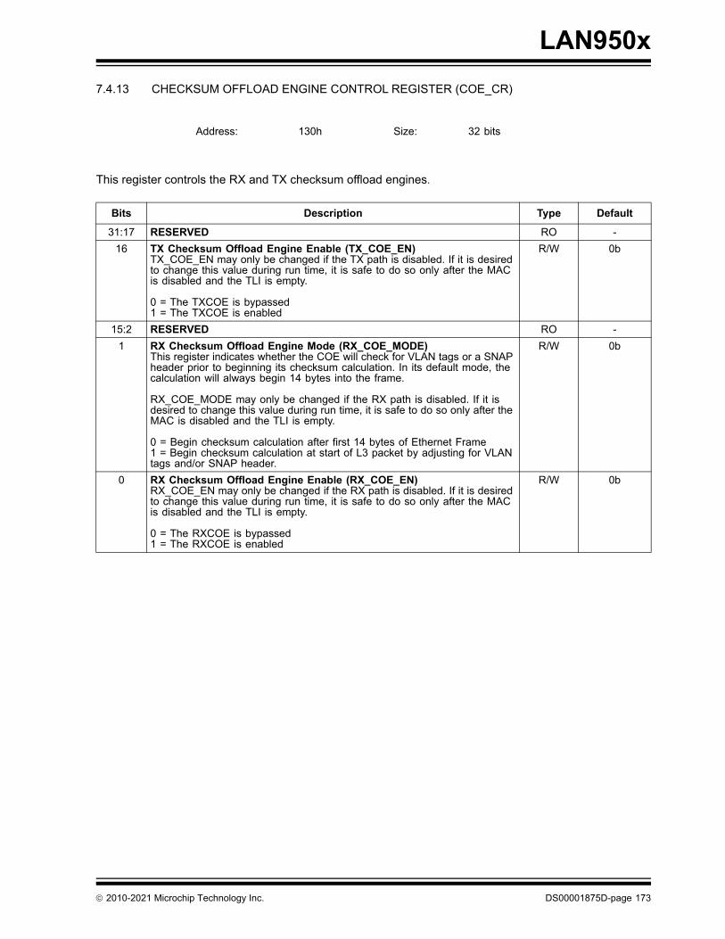
LAN950x
7.4.13 CHECKSUM OFFLOAD ENGINE CONTROL REGISTER (COE_CR)
This register controls the RX and TX checksum offload engines.
Address: 130h Size: 32 bits
Bits Description Type Default
31:17 RESERVED RO -
16 TX Checksum Offload Engine Enable (TX_COE_EN)TX_COE_EN may only be changed if the TX path is disabled. If it is desired to change this value during run time, it is safe to do so only after the MAC is disabled and the TLI is empty.
0 = The TXCOE is bypassed1 = The TXCOE is enabled
R/W 0b
15:2 RESERVED RO -
1 RX Checksum Offload Engine Mode (RX_COE_MODE)This register indicates whether the COE will check for VLAN tags or a SNAP header prior to beginning its checksum calculation. In its default mode, the calculation will always begin 14 bytes into the frame.
RX_COE_MODE may only be changed if the RX path is disabled. If it is desired to change this value during run time, it is safe to do so only after the MAC is disabled and the TLI is empty.
0 = Begin checksum calculation after first 14 bytes of Ethernet Frame1 = Begin checksum calculation at start of L3 packet by adjusting for VLAN tags and/or SNAP header.
R/W 0b
0 RX Checksum Offload Engine Enable (RX_COE_EN)RX_COE_EN may only be changed if the RX path is disabled. If it is desired to change this value during run time, it is safe to do so only after the MAC is disabled and the TLI is empty.
0 = The RXCOE is bypassed1 = The RXCOE is enabled
R/W 0b
2010-2021 Microchip Technology Inc. DS00001875D-page 173
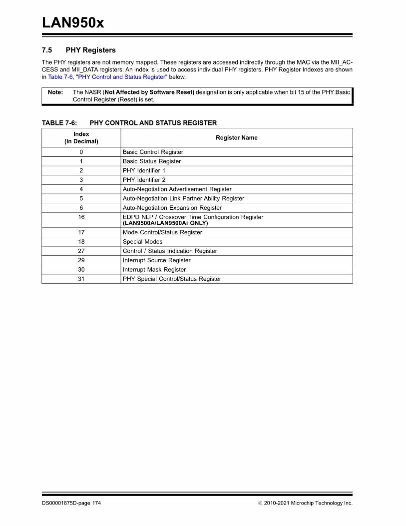
LAN950x
7.5 PHY Registers
The PHY registers are not memory mapped. These registers are accessed indirectly through the MAC via the MII_AC-CESS and MII_DATA registers. An index is used to access individual PHY registers. PHY Register Indexes are shownin Table 7-6, "PHY Control and Status Register" below.
Note: The NASR (Not Affected by Software Reset) designation is only applicable when bit 15 of the PHY BasicControl Register (Reset) is set.
TABLE 7-6: PHY CONTROL AND STATUS REGISTER
Index(In Decimal)
Register Name
0 Basic Control Register
1 Basic Status Register
2 PHY Identifier 1
3 PHY Identifier 2
4 Auto-Negotiation Advertisement Register
5 Auto-Negotiation Link Partner Ability Register
6 Auto-Negotiation Expansion Register
16 EDPD NLP / Crossover Time Configuration Register (LAN9500A/LAN9500Ai ONLY)
17 Mode Control/Status Register
18 Special Modes
27 Control / Status Indication Register
29 Interrupt Source Register
30 Interrupt Mask Register
31 PHY Special Control/Status Register
DS00001875D-page 174 2010-2021 Microchip Technology Inc.
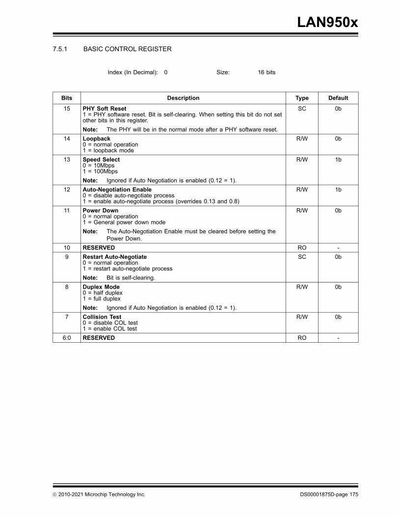
LAN950x
7.5.1 BASIC CONTROL REGISTER
Index (In Decimal): 0 Size: 16 bits
Bits Description Type Default
15 PHY Soft Reset1 = PHY software reset. Bit is self-clearing. When setting this bit do not set other bits in this register.
Note: The PHY will be in the normal mode after a PHY software reset.
SC 0b
14 Loopback0 = normal operation1 = loopback mode
R/W 0b
13 Speed Select0 = 10Mbps1 = 100Mbps
Note: Ignored if Auto Negotiation is enabled (0.12 = 1).
R/W 1b
12 Auto-Negotiation Enable0 = disable auto-negotiate process1 = enable auto-negotiate process (overrides 0.13 and 0.8)
R/W 1b
11 Power Down0 = normal operation 1 = General power down mode
Note: The Auto-Negotiation Enable must be cleared before setting the Power Down.
R/W 0b
10 RESERVED RO -
9 Restart Auto-Negotiate0 = normal operation1 = restart auto-negotiate process
Note: Bit is self-clearing.
SC 0b
8 Duplex Mode0 = half duplex1 = full duplex
Note: Ignored if Auto Negotiation is enabled (0.12 = 1).
R/W 0b
7 Collision Test0 = disable COL test1 = enable COL test
R/W 0b
6:0 RESERVED RO -
2010-2021 Microchip Technology Inc. DS00001875D-page 175
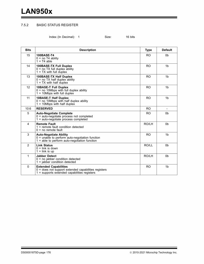
LAN950x
7.5.2 BASIC STATUS REGISTER
Index (In Decimal): 1 Size: 16 bits
Bits Description Type Default
15 100BASE-T40 = no T4 ability1 = T4 able
RO 0b
14 100BASE-TX Full Duplex0 = no TX full duplex ability1 = TX with full duplex
RO 1b
13 100BASE-TX Half Duplex0 = no TX half duplex ability1 = TX with half duplex
RO 1b
12 10BASE-T Full Duplex0 = no 10Mbps with full duplex ability1 = 10Mbps with full duplex
RO 1b
11 10BASE-T Half Duplex0 = no 10Mbps with half duplex ability1 = 10Mbps with half duplex
RO 1b
10:6 RESERVED RO -
5 Auto-Negotiate Complete0 = auto-negotiate process not completed1 = auto-negotiate process completed
RO 0b
4 Remote Fault1 = remote fault condition detected0 = no remote fault
RO/LH 0b
3 Auto-Negotiate Ability0 = unable to perform auto-negotiation function1 = able to perform auto-negotiation function
RO 1b
2 Link Status0 = link is down1 = link is up
RO/LL 0b
1 Jabber Detect0 = no jabber condition detected1 = jabber condition detected
RO/LH 0b
0 Extended Capabilities0 = does not support extended capabilities registers1 = supports extended capabilities registers
RO 1b
DS00001875D-page 176 2010-2021 Microchip Technology Inc.
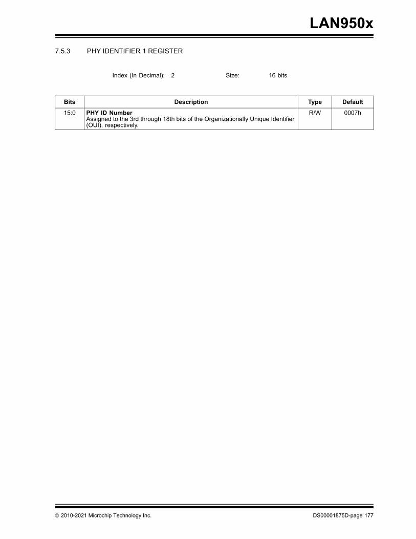
LAN950x
7.5.3 PHY IDENTIFIER 1 REGISTER
Index (In Decimal): 2 Size: 16 bits
Bits Description Type Default
15:0 PHY ID NumberAssigned to the 3rd through 18th bits of the Organizationally Unique Identifier (OUI), respectively.
R/W 0007h
2010-2021 Microchip Technology Inc. DS00001875D-page 177
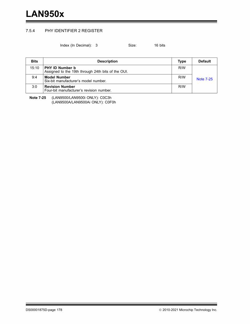
LAN950x
7.5.4 PHY IDENTIFIER 2 REGISTER
Note 7-25 (LAN9500/LAN9500i ONLY): C0C3h(LAN9500A/LAN9500Ai ONLY): C0F0h
Index (In Decimal): 3 Size: 16 bits
Bits Description Type Default
15:10 PHY ID Number bAssigned to the 19th through 24th bits of the OUI.
R/W
Note 7-259:4 Model NumberSix-bit manufacturer’s model number.
R/W
3:0 Revision NumberFour-bit manufacturer’s revision number.
R/W
DS00001875D-page 178 2010-2021 Microchip Technology Inc.
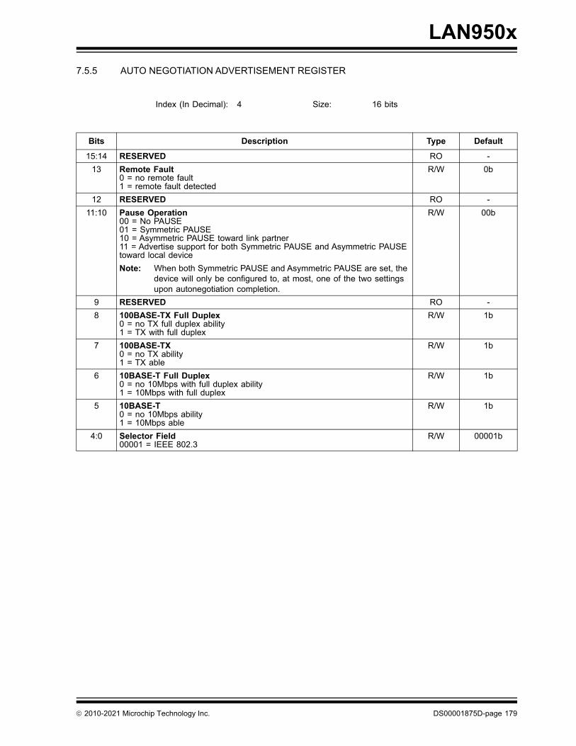
LAN950x
7.5.5 AUTO NEGOTIATION ADVERTISEMENT REGISTER
Index (In Decimal): 4 Size: 16 bits
Bits Description Type Default
15:14 RESERVED RO -
13 Remote Fault0 = no remote fault1 = remote fault detected
R/W 0b
12 RESERVED RO -
11:10 Pause Operation00 = No PAUSE 01 = Symmetric PAUSE10 = Asymmetric PAUSE toward link partner11 = Advertise support for both Symmetric PAUSE and Asymmetric PAUSE toward local device
Note: When both Symmetric PAUSE and Asymmetric PAUSE are set, the device will only be configured to, at most, one of the two settings upon autonegotiation completion.
R/W 00b
9 RESERVED RO -
8 100BASE-TX Full Duplex0 = no TX full duplex ability1 = TX with full duplex
R/W 1b
7 100BASE-TX0 = no TX ability1 = TX able
R/W 1b
6 10BASE-T Full Duplex0 = no 10Mbps with full duplex ability1 = 10Mbps with full duplex
R/W 1b
5 10BASE-T0 = no 10Mbps ability1 = 10Mbps able
R/W 1b
4:0 Selector Field00001 = IEEE 802.3
R/W 00001b
2010-2021 Microchip Technology Inc. DS00001875D-page 179
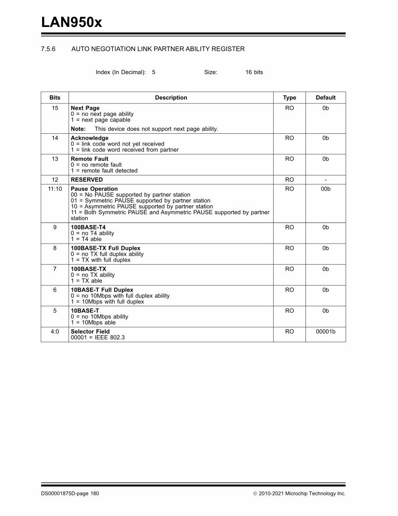
LAN950x
7.5.6 AUTO NEGOTIATION LINK PARTNER ABILITY REGISTER
Index (In Decimal): 5 Size: 16 bits
Bits Description Type Default
15 Next Page0 = no next page ability1 = next page capable
Note: This device does not support next page ability.
RO 0b
14 Acknowledge0 = link code word not yet received1 = link code word received from partner
RO 0b
13 Remote Fault0 = no remote fault1 = remote fault detected
RO 0b
12 RESERVED RO -
11:10 Pause Operation00 = No PAUSE supported by partner station01 = Symmetric PAUSE supported by partner station10 = Asymmetric PAUSE supported by partner station11 = Both Symmetric PAUSE and Asymmetric PAUSE supported by partner station
RO 00b
9 100BASE-T40 = no T4 ability1 = T4 able
RO 0b
8 100BASE-TX Full Duplex0 = no TX full duplex ability1 = TX with full duplex
RO 0b
7 100BASE-TX0 = no TX ability1 = TX able
RO 0b
6 10BASE-T Full Duplex0 = no 10Mbps with full duplex ability1 = 10Mbps with full duplex
RO 0b
5 10BASE-T0 = no 10Mbps ability1 = 10Mbps able
RO 0b
4:0 Selector Field00001 = IEEE 802.3
RO 00001b
DS00001875D-page 180 2010-2021 Microchip Technology Inc.
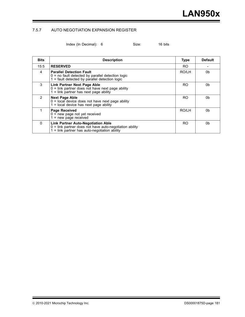
LAN950x
7.5.7 AUTO NEGOTIATION EXPANSION REGISTER
Index (In Decimal): 6 Size: 16 bits
Bits Description Type Default
15:5 RESERVED RO -
4 Parallel Detection Fault0 = no fault detected by parallel detection logic1 = fault detected by parallel detection logic
RO/LH 0b
3 Link Partner Next Page Able0 = link partner does not have next page ability1 = link partner has next page ability
RO 0b
2 Next Page Able0 = local device does not have next page ability1 = local device has next page ability
RO 0b
1 Page Received0 = new page not yet received1 = new page received
RO/LH 0b
0 Link Partner Auto-Negotiation Able0 = link partner does not have auto-negotiation ability1 = link partner has auto-negotiation ability
RO 0b
2010-2021 Microchip Technology Inc. DS00001875D-page 181
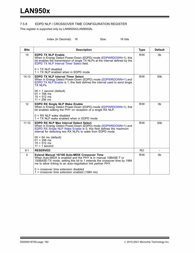
LAN950x
7.5.8 EDPD NLP / CROSSOVER TIME CONFIGURATION REGISTER
This register is supported only by LAN9500A/LAN9500Ai.
Index (In Decimal): 16 Size: 16 bits
Bits Description Type Default
15 EDPD TX NLP EnableWhen in Energy Detect Power-Down (EDPD) mode (EDPWRDOWN=1), this bit enables the transmission of single TX NLPs at the interval defined by the EDPD TX NLP Interval Timer Select field.
0 = TX NLP disabled1 = TX NLP enabled when in EDPD mode
R/W 0b
14:13 EDPD TX NLP Interval Timer SelectWhen in Energy Detect Power-Down (EDPD) mode (EDPWRDOWN=1) and EDPD TX NLP Enable is 1, this field defines the interval used to send single TX NLPs.
00 = 1 second (default)01 = 768 ms10 = 512 ms11 = 256 ms
R/W 00b
12 EDPD RX Single NLP Wake EnableWhen in Energy Detect Power-Down (EDPD) mode (EDPWRDOWN=1), this bit enables waking the PHY on reception of a single RX NLP.
0 = RX NLP wake disabled1 = TX NLP wake enabled when in EDPD mode
R/W 0b
11:10 EDPD RX NLP Max Interval Detect SelectWhen in Energy Detect Power-Down (EDPD) mode (EDPWRDOWN=1) and EDPD RX Single NLP Wake Enable is 0, this field defines the maximum interval for detecting two RX NLPs to wake from EDPD mode
00 = 64 ms (default)01 = 256 ms10 = 512 ms11 = 1 second
R/W 00b
9:1 RESERVED RO -
0 Extend Manual 10/100 Auto-MDIX Crossover TimeWhen Auto-MIDX is enabled and the PHY is in manual 10BASE-T or 100BASE-TX mode, setting this bit to 1 extends the crossover time by 1984 ms to allow linking to an auto-negotiation link partner PHY.
0 = crossover time extension disabled1 = crossover time extension enabled (1984 ms)
R/W 0b
DS00001875D-page 182 2010-2021 Microchip Technology Inc.
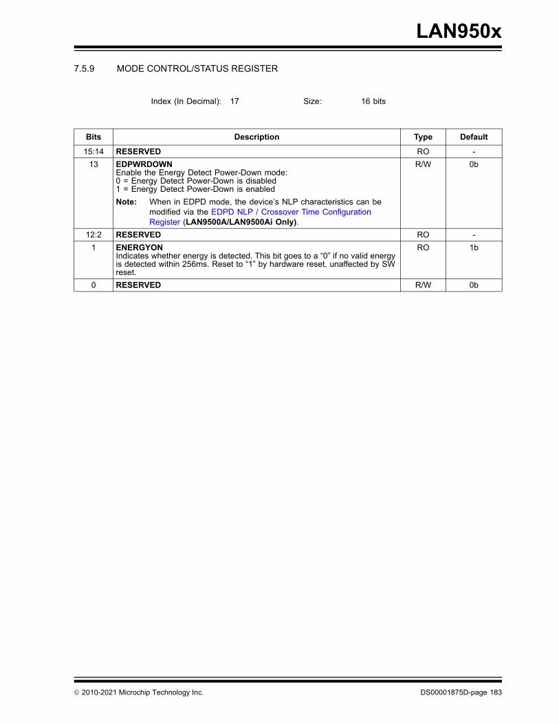
LAN950x
7.5.9 MODE CONTROL/STATUS REGISTER
Index (In Decimal): 17 Size: 16 bits
Bits Description Type Default
15:14 RESERVED RO -
13 EDPWRDOWNEnable the Energy Detect Power-Down mode:0 = Energy Detect Power-Down is disabled1 = Energy Detect Power-Down is enabled
Note: When in EDPD mode, the device’s NLP characteristics can be modified via the EDPD NLP / Crossover Time Configuration Register (LAN9500A/LAN9500Ai Only).
R/W 0b
12:2 RESERVED RO -
1 ENERGYONIndicates whether energy is detected. This bit goes to a “0” if no valid energy is detected within 256ms. Reset to “1” by hardware reset, unaffected by SW reset.
RO 1b
0 RESERVED R/W 0b
2010-2021 Microchip Technology Inc. DS00001875D-page 183
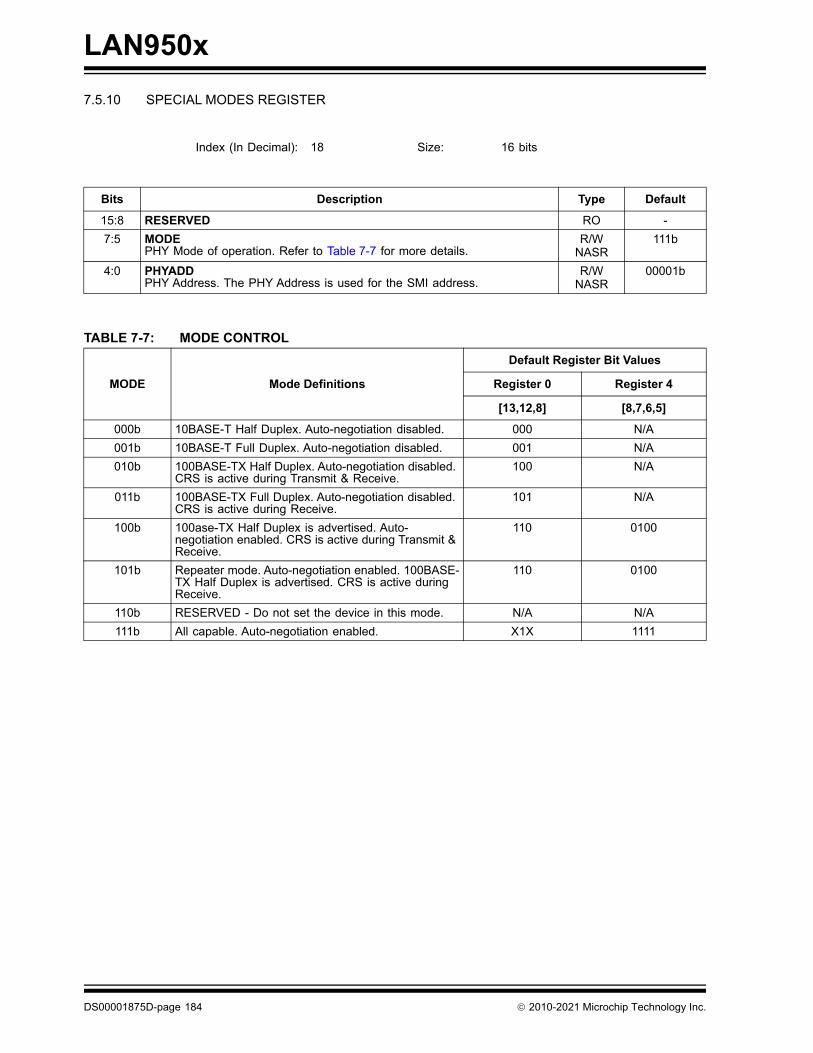
LAN950x
7.5.10 SPECIAL MODES REGISTER
Index (In Decimal): 18 Size: 16 bits
Bits Description Type Default
15:8 RESERVED RO -
7:5 MODEPHY Mode of operation. Refer to Table 7-7 for more details.
R/WNASR
111b
4:0 PHYADDPHY Address. The PHY Address is used for the SMI address.
R/WNASR
00001b
TABLE 7-7: MODE CONTROL
MODE Mode Definitions
Default Register Bit Values
Register 0 Register 4
[13,12,8] [8,7,6,5]
000b 10BASE-T Half Duplex. Auto-negotiation disabled. 000 N/A
001b 10BASE-T Full Duplex. Auto-negotiation disabled. 001 N/A
010b 100BASE-TX Half Duplex. Auto-negotiation disabled. CRS is active during Transmit & Receive.
100 N/A
011b 100BASE-TX Full Duplex. Auto-negotiation disabled. CRS is active during Receive.
101 N/A
100b 100ase-TX Half Duplex is advertised. Auto-negotiation enabled. CRS is active during Transmit & Receive.
110 0100
101b Repeater mode. Auto-negotiation enabled. 100BASE-TX Half Duplex is advertised. CRS is active during Receive.
110 0100
110b RESERVED - Do not set the device in this mode. N/A N/A
111b All capable. Auto-negotiation enabled. X1X 1111
DS00001875D-page 184 2010-2021 Microchip Technology Inc.
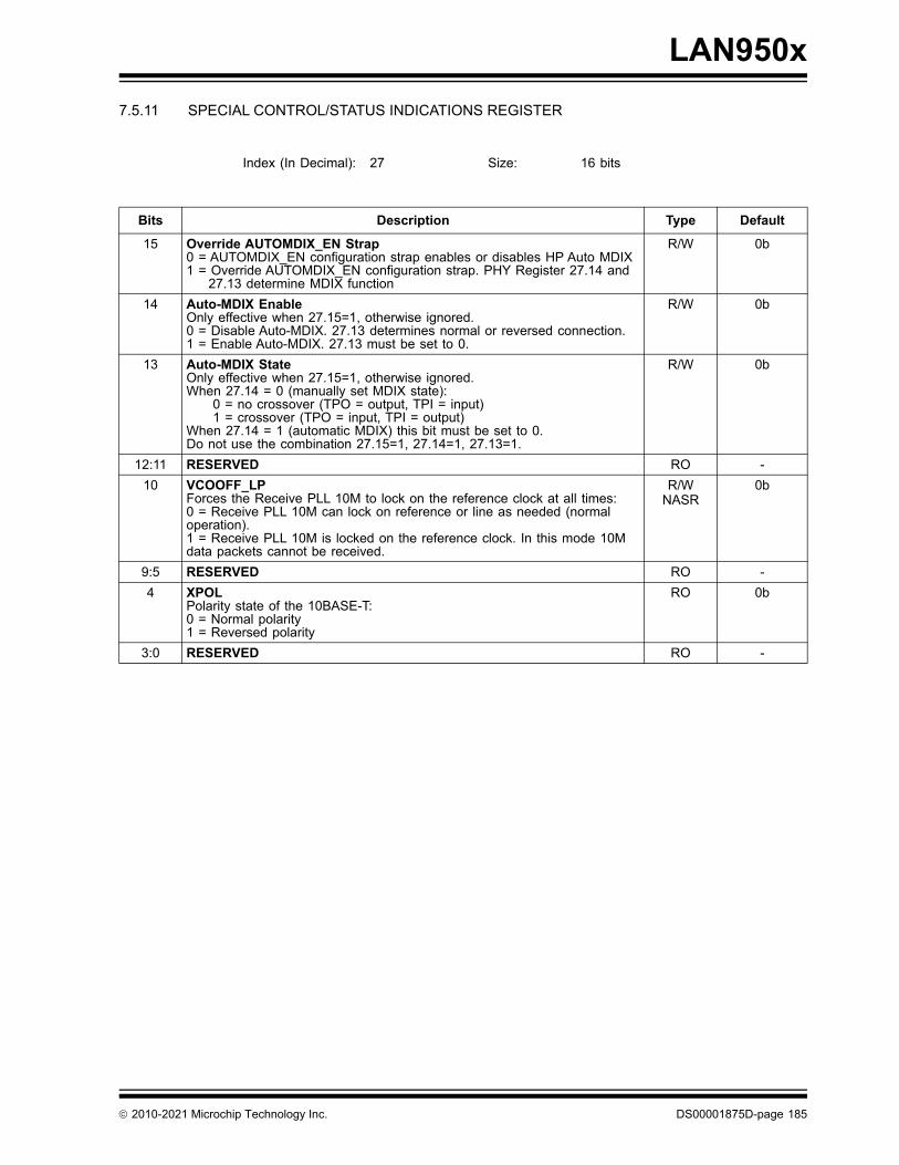
LAN950x
7.5.11 SPECIAL CONTROL/STATUS INDICATIONS REGISTER
Index (In Decimal): 27 Size: 16 bits
Bits Description Type Default
15 Override AUTOMDIX_EN Strap0 = AUTOMDIX_EN configuration strap enables or disables HP Auto MDIX1 = Override AUTOMDIX_EN configuration strap. PHY Register 27.14 and
27.13 determine MDIX function
R/W 0b
14 Auto-MDIX EnableOnly effective when 27.15=1, otherwise ignored.0 = Disable Auto-MDIX. 27.13 determines normal or reversed connection.1 = Enable Auto-MDIX. 27.13 must be set to 0.
R/W 0b
13 Auto-MDIX StateOnly effective when 27.15=1, otherwise ignored.When 27.14 = 0 (manually set MDIX state):
0 = no crossover (TPO = output, TPI = input)1 = crossover (TPO = input, TPI = output)
When 27.14 = 1 (automatic MDIX) this bit must be set to 0.Do not use the combination 27.15=1, 27.14=1, 27.13=1.
R/W 0b
12:11 RESERVED RO -
10 VCOOFF_LPForces the Receive PLL 10M to lock on the reference clock at all times:0 = Receive PLL 10M can lock on reference or line as needed (normal operation).1 = Receive PLL 10M is locked on the reference clock. In this mode 10M data packets cannot be received.
R/WNASR
0b
9:5 RESERVED RO -
4 XPOLPolarity state of the 10BASE-T:0 = Normal polarity1 = Reversed polarity
RO 0b
3:0 RESERVED RO -
2010-2021 Microchip Technology Inc. DS00001875D-page 185
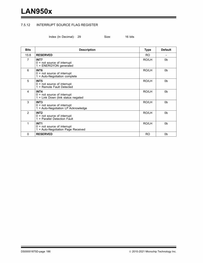
LAN950x
7.5.12 INTERRUPT SOURCE FLAG REGISTER
Index (In Decimal): 29 Size: 16 bits
Bits Description Type Default
15:8 RESERVED RO -
7 INT70 = not source of interrupt1 = ENERGYON generated
RO/LH 0b
6 INT60 = not source of interrupt1 = Auto-Negotiation complete
RO/LH 0b
5 INT50 = not source of interrupt1 = Remote Fault Detected
RO/LH 0b
4 INT40 = not source of interrupt1 = Link Down (link status negated
RO/LH 0b
3 INT30 = not source of interrupt1 = Auto-Negotiation LP Acknowledge
RO/LH 0b
2 INT20 = not source of interrupt1 = Parallel Detection Fault
RO/LH 0b
1 INT10 = not source of interrupt1 = Auto-Negotiation Page Received
RO/LH 0b
0 RESERVED RO 0b
DS00001875D-page 186 2010-2021 Microchip Technology Inc.
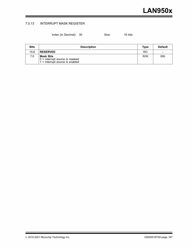
LAN950x
7.5.13 INTERRUPT MASK REGISTER
Index (In Decimal): 30 Size: 16 bits
Bits Description Type Default
15:8 RESERVED RO -
7:0 Mask Bits0 = interrupt source is masked1 = interrupt source is enabled
R/W 00h
2010-2021 Microchip Technology Inc. DS00001875D-page 187
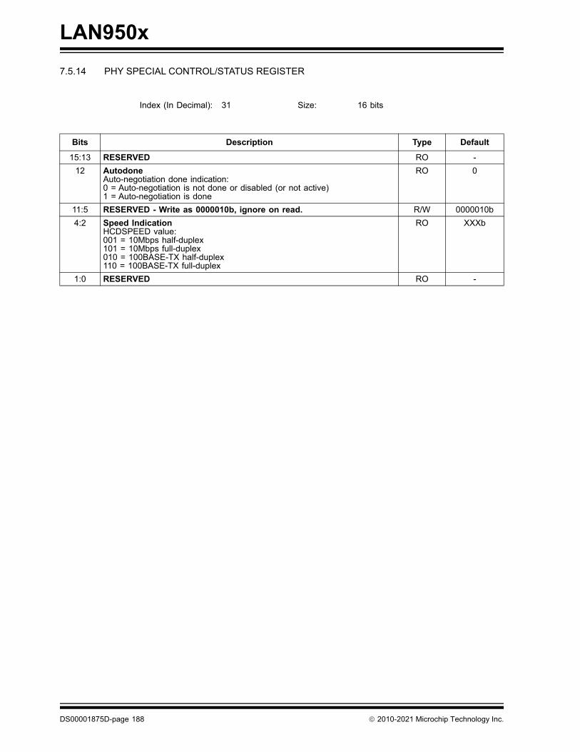
LAN950x
7.5.14 PHY SPECIAL CONTROL/STATUS REGISTER
Index (In Decimal): 31 Size: 16 bits
Bits Description Type Default
15:13 RESERVED RO -
12 AutodoneAuto-negotiation done indication:0 = Auto-negotiation is not done or disabled (or not active)1 = Auto-negotiation is done
RO 0
11:5 RESERVED - Write as 0000010b, ignore on read. R/W 0000010b
4:2 Speed IndicationHCDSPEED value:001 = 10Mbps half-duplex101 = 10Mbps full-duplex010 = 100BASE-TX half-duplex110 = 100BASE-TX full-duplex
RO XXXb
1:0 RESERVED RO -
DS00001875D-page 188 2010-2021 Microchip Technology Inc.
LAN950x
8.0 OPERATIONAL CHARACTERISTICS
8.1 Absolute Maximum Ratings*
Supply Voltage (VDD33IO, VDD33A) (Note 8-1) ........................................................................................ 0V to +3.6V
Positive voltage on signal pins, with respect to ground (Note 8-2) ......................................................................... +6V
Negative voltage on signal pins, with respect to ground (Note 8-3)...................................................................... -0.5V
Positive voltage on XI, with respect to ground ................................................................................................. Note 8-4
Positive voltage on XO, with respect to ground ................................................................................................... +2.5V
Ambient Operating Temperature in Still Air (TA).............................................................................................. Note 8-5
Storage Temperature ......................................................................................................................... .-55oC to +150oC
Lead Temperature Range ........................................................................................Refer to JEDEC Spec. J-STD-020
HBM ESD Performance .................................................................................................................................. .Note 8-6
IEC61000-4-2 Contact Discharge ESD Performance (Note 8-7) ....................................................................... .+/-8kV
IEC61000-4-2 Air-Gap Discharge ESD Performance (Note 8-7) ..................................................................... .+/-15kV
Note 8-1 When powering this device from laboratory or system power supplies, it is important that the absolutemaximum ratings not be exceeded or device failure can result. Some power supplies exhibit voltagespikes on their outputs when AC power is switched on or off. In addition, voltage transients on theAC power line may appear on the DC output. If this possibility exists, it is suggested that a clampcircuit be used.
Note 8-2 This rating does not apply to the following pins: XI, XO, EXRES, USBRBIAS.
Note 8-3 This rating does not apply to the following pins: EXRES, USBRBIAS.
Note 8-4 +4.6V for LAN9500/LAN9500i, VDDCORE for LAN9500A/LAN9500Ai
Note 8-5 0oC to +70oC for commercial version, -40oC to +85oC for industrial version.
Note 8-6 +/-8kV for LAN9500/LAN9500i, +/-5kV for LAN9500A/LAN9500Ai
Note 8-7 Performed by independent 3rd party test facility.
*Stresses exceeding those listed in this section could cause permanent damage to the device. This is a stress ratingonly. Exposure to absolute maximum rating conditions for extended periods may affect device reliability. Functionaloperation of the device at any condition exceeding those indicated in Section 8.2, "Operating Conditions**", Section 8.5,"DC Specifications", or any other applicable section of this specification is not implied. Note, device signals are NOT 5volt tolerant unless specified otherwise.
8.2 Operating Conditions**
Supply Voltage (VDD33A, VDD33BIAS, VDD33IO)............................................................................ +3.3V +/- 300mV
Ambient Operating Temperature in Still Air (TA).............................................................................................. Note 8-5
**Proper operation of the device is guaranteed only within the ranges specified in this section.
2010-2021 Microchip Technology Inc. DS00001875D-page 189
LAN950x
8.3 Package Thermal Specifications
8.4 Power Consumption
This section details the power consumption of the device as measured during various modes of operation. Power con-sumption values are provided for both the device-only, and for the device plus Ethernet components. Power dissipationis determined by temperature, supply voltage, and external source/sink requirements.
8.4.1 SUSPEND0
8.4.2 SUSPEND1
FIGURE 8-1: 56-QFN PACKAGE THERMAL PARAMETERS
Symbol °C/W Notes
JA
30 0 meters/seconds
26 1 meters/seconds
23 2.5 meters/seconds
JC 4.8
JB 17
JT 0.3
JB 16
Note: All current consumption and power dissipation values were measured at VDD33IO and VDD33A equal to3.3V.
TABLE 8-1: POWER CONSUMPTION/DISSIPATION - SUSPEND0 (LAN9500/LAN9500I)
Parameter MIN Typical MAX Unit
Supply current (VDD33IO, VDD33A) (Device Only) 78 mA
Power Dissipation (Device Only) 257 mW
Power Dissipation (Device and Ethernet components) 395 mW
TABLE 8-2: POWER CONSUMPTION/DISSIPATION - SUSPEND0 (LAN9500A/LAN9500AI)
Parameter MIN Typical MAX Unit
Supply current (VDD33IO, VDD33A) (Device Only) 46 mA
Power Dissipation (Device Only) 152 mW
Power Dissipation (Device and Ethernet components) 291 mW
TABLE 8-3: POWER CONSUMPTION/DISSIPATION - SUSPEND1 (LAN9500/LAN9500I)
Parameter MIN Typical MAX Unit
Supply current (VDD33IO, VDD33A) (Device Only) 20 mA
Power Dissipation (Device Only) 66 mW
Power Dissipation (Device and Ethernet components) 66 mW
DS00001875D-page 190 2010-2021 Microchip Technology Inc.
LAN950x
8.4.3 SUSPEND2
8.4.4 SUSPEND3
8.4.5 OPERATIONAL
TABLE 8-4: POWER CONSUMPTION/DISSIPATION - SUSPEND1 (LAN9500A/LAN9500AI)
Parameter MIN Typical MAX Unit
Supply current (VDD33IO, VDD33A) (Device Only) 7.0 mA
Power Dissipation (Device Only) 23.5 mW
Power Dissipation (Device and Ethernet components) 27.5 mW
TABLE 8-5: POWER CONSUMPTION/DISSIPATION - SUSPEND2 (LAN9500/LAN9500I)
Parameter MIN Typical MAX Unit
Supply current (VDD33IO, VDD33A) (Device Only) 0.624 mA
Power Dissipation (Device Only) 2.1 mW
Power Dissipation (Device and Ethernet components) 2.1 mW
TABLE 8-6: POWER CONSUMPTION/DISSIPATION - SUSPEND2 (LAN9500A/LAN9500AI)
Parameter MIN Typical MAX Unit
Supply current (VDD33IO, VDD33A) (Device Only) 1.6 mA
Power Dissipation (Device Only) 5.3 mW
Power Dissipation (Device and Ethernet components) 5.3 mW
Note: SUSPEND2 power consumption/dissipation values were measured in bus-powered mode.
Note: SUSPEND3 not supported by LAN9500/LAN9500i.
TABLE 8-7: POWER CONSUMPTION/DISSIPATION - SUSPEND3 (LAN9500A/LAN9500AI)
Parameter MIN Typical MAX Unit
Supply current (VDD33IO, VDD33A) (Device Only) 24.5 mA
Power Dissipation (Device Only) 81.2 mW
Power Dissipation (Device and Ethernet components) 85.1 mW
TABLE 8-8: OPERATIONAL POWER CONSUMPTION/DISSIPATION (LAN9500/LAN9500I)
Parameter MIN Typical MAX Unit
100BASE-TX Full Duplex (USB High-Speed)
Supply current (VDD33IO, VDD33A) (Device Only) 143 mA
Power Dissipation (Device Only) 474 mW
Power Dissipation (Device and Ethernet components) 618 mW
10BASE-T Full Duplex (USB High-Speed)
Supply current (VDD33IO, VDD33A) (Device Only) 103 mA
Power Dissipation (Device Only) 342 mW
Power Dissipation (Device and Ethernet components) 692 mW
2010-2021 Microchip Technology Inc. DS00001875D-page 191
LAN950x
8.4.6 CUSTOMER EVALUATION BOARD OPERATIONAL CURRENT CONSUMPTION***
***Total system current consumption as measured on the 5V USB VBUS input to a bus-powered Customer EvaluationBoard, where VBUS = 5.0V and VDD33IO = VDD33A = 3.3V.
100BASE-TX Full Duplex (USB Full-Speed)
Supply current (VDD33IO, VDD33A) (Device Only) 139 mA
Power Dissipation (Device Only) 460 mW
Power Dissipation (Device and Ethernet components) 605 mW
10BASE-T Full Duplex (USB Full-Speed)
Supply current (VDD33IO, VDD33A) (Device Only) 98 mA
Power Dissipation (Device Only) 324 mW
Power Dissipation (Device and Ethernet components) 673 mW
TABLE 8-9: OPERATIONAL POWER CONSUMPTION/DISSIPATION (LAN9500A/LAN9500AI)
Parameter MIN Typical MAX Unit
100BASE-TX Full Duplex (USB High-Speed)
Supply current (VDD33IO, VDD33A) (Device Only) 69 mA
Power Dissipation (Device Only) 228 mW
Power Dissipation (Device and Ethernet components) 367 mW
10BASE-T Full Duplex (USB High-Speed)
Supply current (VDD33IO, VDD33A) (Device Only) 45 mA
Power Dissipation (Device Only) 149 mW
Power Dissipation (Device and Ethernet components) 489 mW
100BASE-TX Full Duplex (USB Full-Speed)
Supply current (VDD33IO, VDD33A) (Device Only) 66 mA
Power Dissipation (Device Only) 218 mW
Power Dissipation (Device and Ethernet components) 356 mW
10BASE-T Full Duplex (USB Full-Speed)
Supply current (VDD33IO, VDD33A) (Device Only) 43 mA
Power Dissipation (Device Only) 142 mW
Power Dissipation (Device and Ethernet components) 483 mW
TABLE 8-10: CEB OPERATIONAL CURRENT CONSUMPTION (LAN9500/LAN9500I)
Parameter MIN Typical MAX Unit
100BASE-TX Full Duplex (USB High-Speed)
Total Microchip Customer Evaluation Board Current Consumption 208 mA
TABLE 8-11: CEB OPERATIONAL CURRENT CONSUMPTION (LAN9500A/LAN9500AI)
Parameter MIN Typical MAX Unit
100BASE-TX Full Duplex (USB High-Speed)
Total Microchip Customer Evaluation Board Current Consumption 150 mA
TABLE 8-8: OPERATIONAL POWER CONSUMPTION/DISSIPATION (LAN9500/LAN9500I)
Parameter MIN Typical MAX Unit
DS00001875D-page 192 2010-2021 Microchip Technology Inc.
LAN950x
8.5 DC Specifications
TABLE 8-12: I/O BUFFER CHARACTERISTICS
Parameter Symbol MIN TYP MAX Units Notes
IS Type Input Buffer
Low Input Level
High Input Level
Negative-Going Threshold
Positive-Going Threshold
SchmittTrigger Hysteresis (VIHT - VILT)
Input Leakage(VIN = VSS or VDD33IO)
Input Capacitance
VILI
VIHI
VILT
VIHT
VHYS
IIH
CIN
-0.3
1.01
1.39
336
-10
1.19
1.59
399
3.6
1.39
1.8
485
10
3
V
V
V
V
mV
µA
pF
Schmitt trigger
Schmitt trigger
Note 8-1
IS_5V Type Input Buffer
Low Input Level
High Input Level
Negative-Going Threshold
Positive-Going Threshold
SchmittTrigger Hysteresis (VIHT - VILT)
Input Leakage(VIN = VSS or VDD33IO)
Input Leakage(VIN = 5.5V)
Input Capacitance
VILI
VIHI
VILT
VIHT
VHYS
IIH
IIH
CIN
-0.3
1.01
1.39
336
-10
1.19
1.59
399
5.5
1.39
1.8
485
10
79
4
V
V
V
V
mV
µA
µA
pF
Schmitt trigger
Schmitt trigger
Note 8-1
Note 8-1, Note 8-2
O8 Type Buffers
Low Output Level
High Output Level
VOL
VOH VDD33IO - 0.4
0.4 V
V
IOL = 8mA
IOH = -8mA
OD8 Type Buffer
Low Output Level VOL 0.4 V IOL = 8mA
O12 Type Buffers
Low Output Level
High Output Level
VOL
VOH VDD33IO - 0.4
0.4 V
V
IOL = 12mA
IOH = -12mA
OD12 Type Buffer
Low Output Level VOL 0.4 V IOL = 12mA
ICLK Type Buffer (XI Input)
Low Input Level
High Input Level
VILI
VIHI
-0.3
Note 8-4
0.5 V
Note 8-3
2010-2021 Microchip Technology Inc. DS00001875D-page 193
LAN950x
Note 8-1 This specification applies to all inputs and tri-stated bi-directional pins. Internal pull-down and pull-upresistors add +/- 50 µA per-pin (typical).
Note 8-2 This is the total 5.5V input leakage for the entire device.
Note 8-3 XI can optionally be driven from a 25 MHz single-ended clock oscillator.
Note 8-4 +1.4V for LAN9500/LAN9500i, +0.8V for LAN9500A/LAN9500Ai
Note 8-5 Measured at line side of transformer, line replaced by 100 (+/- 1%) resistor.
Note 8-6 Offset from 16nS pulse width at 50% of pulse peak.
Note 8-7 Measured differentially.
Note 8-8 Min/max voltages guaranteed as measured with 100 resistive load.
TABLE 8-13: 100BASE-TX TRANSCEIVER CHARACTERISTICS
Parameter Symbol MIN TYP MAX Units Notes
Peak Differential Output Voltage High VPPH 950 - 1050 mVpk Note 8-5
Peak Differential Output Voltage Low VPPL -950 - -1050 mVpk Note 8-5
Signal Amplitude Symmetry VSS 98 - 102 % Note 8-5
Signal Rise and Fall Time TRF 3.0 - 5.0 nS Note 8-5
Rise and Fall Symmetry TRFS - - 0.5 nS Note 8-5
Duty Cycle Distortion DCD 35 50 65 % Note 8-6
Overshoot and Undershoot VOS - - 5 %
Jitter 1.4 nS Note 8-7
TABLE 8-14: 10BASE-T TRANSCEIVER CHARACTERISTICS
Parameter Symbol MIN TYP MAX Units Notes
Transmitter Peak Differential Output Voltage VOUT 2.2 2.5 2.8 V Note 8-8
Receiver Differential Squelch Threshold VDS 300 420 585 mV
DS00001875D-page 194 2010-2021 Microchip Technology Inc.
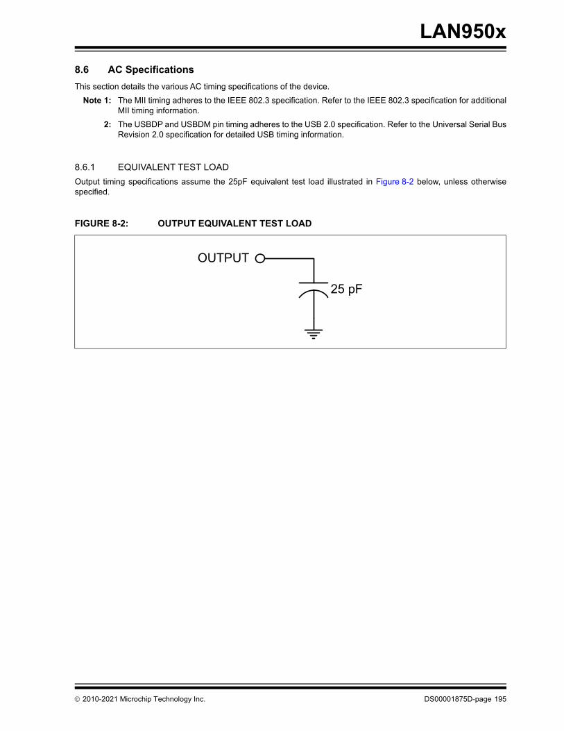
LAN950x
8.6 AC Specifications
This section details the various AC timing specifications of the device.
Note 1: The MII timing adheres to the IEEE 802.3 specification. Refer to the IEEE 802.3 specification for additionalMII timing information.
2: The USBDP and USBDM pin timing adheres to the USB 2.0 specification. Refer to the Universal Serial BusRevision 2.0 specification for detailed USB timing information.
8.6.1 EQUIVALENT TEST LOAD
Output timing specifications assume the 25pF equivalent test load illustrated in Figure 8-2 below, unless otherwisespecified.
FIGURE 8-2: OUTPUT EQUIVALENT TEST LOAD
25 pF
OUTPUT
2010-2021 Microchip Technology Inc. DS00001875D-page 195
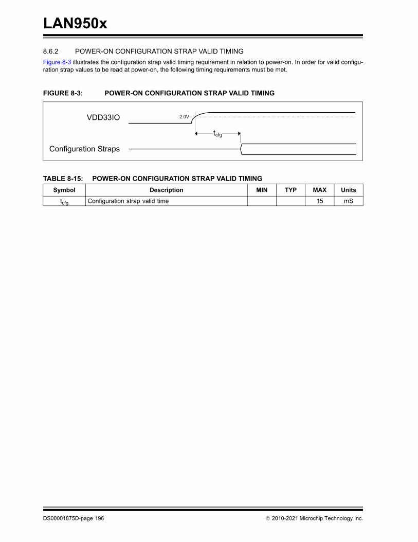
LAN950x
8.6.2 POWER-ON CONFIGURATION STRAP VALID TIMING
Figure 8-3 illustrates the configuration strap valid timing requirement in relation to power-on. In order for valid configu-ration strap values to be read at power-on, the following timing requirements must be met.
FIGURE 8-3: POWER-ON CONFIGURATION STRAP VALID TIMING
TABLE 8-15: POWER-ON CONFIGURATION STRAP VALID TIMING
Symbol Description MIN TYP MAX Units
tcfg Configuration strap valid time 15 mS
VDD33IO
Configuration Straps
tcfg
2.0V
DS00001875D-page 196 2010-2021 Microchip Technology Inc.
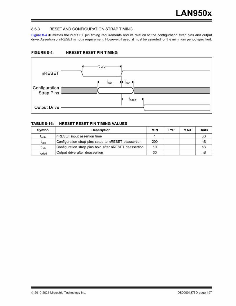
LAN950x
8.6.3 RESET AND CONFIGURATION STRAP TIMING
Figure 8-4 illustrates the nRESET pin timing requirements and its relation to the configuration strap pins and outputdrive. Assertion of nRESET is not a requirement. However, if used, it must be asserted for the minimum period specified.
FIGURE 8-4: NRESET RESET PIN TIMING
TABLE 8-16: NRESET RESET PIN TIMING VALUES
Symbol Description MIN TYP MAX Units
trstia nRESET input assertion time 1 uS
tcss Configuration strap pins setup to nRESET deassertion 200 nS
tcsh Configuration strap pins hold after nRESET deassertion 10 nS
todad Output drive after deassertion 30 nS
tcss
nRESET
Configuration Strap Pins
trstia
tcsh
Output Drive
todad
2010-2021 Microchip Technology Inc. DS00001875D-page 197
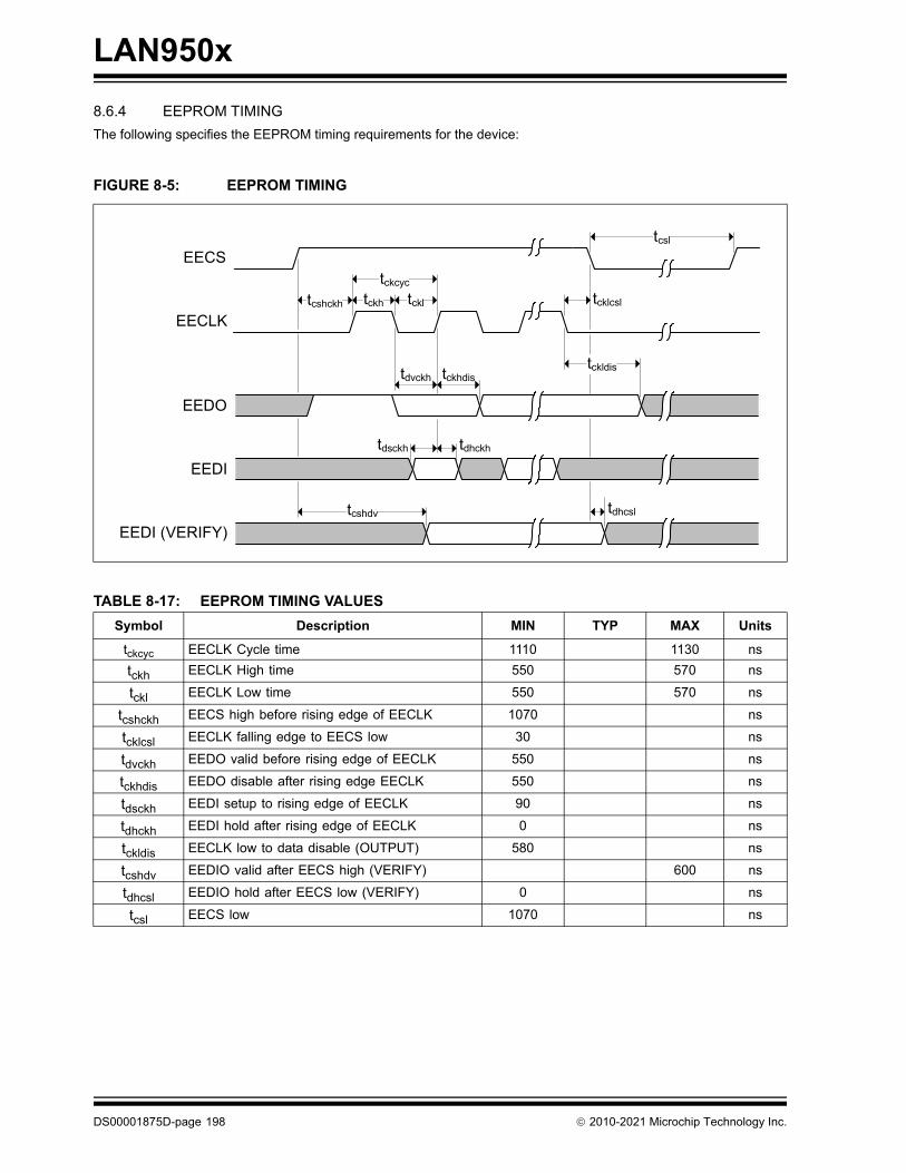
LAN950x
8.6.4 EEPROM TIMING
The following specifies the EEPROM timing requirements for the device:
FIGURE 8-5: EEPROM TIMING
TABLE 8-17: EEPROM TIMING VALUES
Symbol Description MIN TYP MAX Units
tckcyc EECLK Cycle time 1110 1130 ns
tckh EECLK High time 550 570 ns
tckl EECLK Low time 550 570 ns
tcshckh EECS high before rising edge of EECLK 1070 ns
tcklcsl EECLK falling edge to EECS low 30 ns
tdvckh EEDO valid before rising edge of EECLK 550 ns
tckhdis EEDO disable after rising edge EECLK 550 ns
tdsckh EEDI setup to rising edge of EECLK 90 ns
tdhckh EEDI hold after rising edge of EECLK 0 ns
tckldis EECLK low to data disable (OUTPUT) 580 ns
tcshdv EEDIO valid after EECS high (VERIFY) 600 ns
tdhcsl EEDIO hold after EECS low (VERIFY) 0 ns
tcsl EECS low 1070 ns
EECLK
EEDO
EEDI
EECS
tckldis
tcshckh
EEDI (VERIFY)
tckh tckl
tckcyc
tcklcsl
tcsl
tdvckh tckhdis
tdsckh tdhckh
tdhcsltcshdv
DS00001875D-page 198 2010-2021 Microchip Technology Inc.
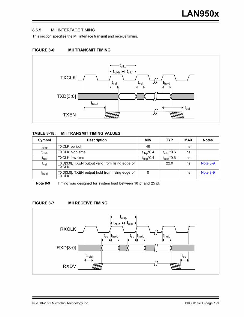
LAN950x
8.6.5 MII INTERFACE TIMING
This section specifies the MII interface transmit and receive timing.
Note 8-9 Timing was designed for system load between 10 pf and 25 pf.
FIGURE 8-6: MII TRANSMIT TIMING
TABLE 8-18: MII TRANSMIT TIMING VALUES
Symbol Description MIN TYP MAX Notes
tclkp TXCLK period 40 ns
tclkh TXCLK high time tclkp*0.4 tclkp*0.6 ns
tclkl TXCLK low time tclkp*0.4 tclkp*0.6 ns
tval TXD[3:0], TXEN output valid from rising edge of TXCLK
22.0 ns Note 8-9
thold TXD[3:0], TXEN output hold from rising edge of TXCLK
0 ns Note 8-9
FIGURE 8-7: MII RECEIVE TIMING
TXCLK
TXD[3:0]
TXEN
tclkh tclkl
tclkp
tval tholdtval
tval
thold
RXCLKtsu
RXD[3:0]
RXDV
tclkh tclkl
tclkp
thold tsu thold thold
tsuthold
2010-2021 Microchip Technology Inc. DS00001875D-page 199
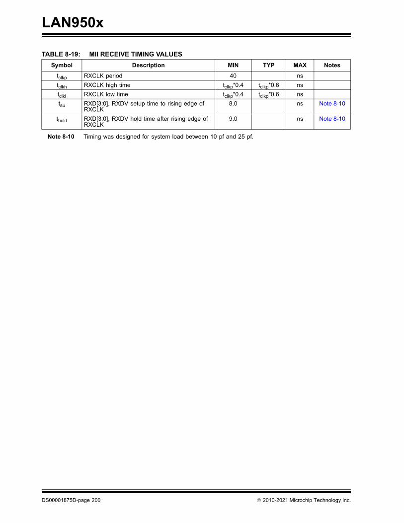
LAN950x
Note 8-10 Timing was designed for system load between 10 pf and 25 pf.
TABLE 8-19: MII RECEIVE TIMING VALUES
Symbol Description MIN TYP MAX Notes
tclkp RXCLK period 40 ns
tclkh RXCLK high time tclkp*0.4 tclkp*0.6 ns
tclkl RXCLK low time tclkp*0.4 tclkp*0.6 ns
tsu RXD[3:0], RXDV setup time to rising edge of RXCLK
8.0 ns Note 8-10
thold RXD[3:0], RXDV hold time after rising edge of RXCLK
9.0 ns Note 8-10
DS00001875D-page 200 2010-2021 Microchip Technology Inc.
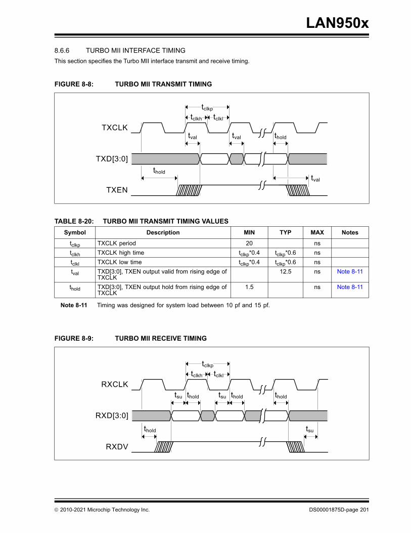
LAN950x
8.6.6 TURBO MII INTERFACE TIMING
This section specifies the Turbo MII interface transmit and receive timing.
Note 8-11 Timing was designed for system load between 10 pf and 15 pf.
FIGURE 8-8: TURBO MII TRANSMIT TIMING
TABLE 8-20: TURBO MII TRANSMIT TIMING VALUES
Symbol Description MIN TYP MAX Notes
tclkp TXCLK period 20 ns
tclkh TXCLK high time tclkp*0.4 tclkp*0.6 ns
tclkl TXCLK low time tclkp*0.4 tclkp*0.6 ns
tval TXD[3:0], TXEN output valid from rising edge of TXCLK
12.5 ns Note 8-11
thold TXD[3:0], TXEN output hold from rising edge of TXCLK
1.5 ns Note 8-11
FIGURE 8-9: TURBO MII RECEIVE TIMING
TXCLK
TXD[3:0]
TXEN
tclkh tclkl
tclkp
tval tholdtval
tval
thold
RXCLKtsu
RXD[3:0]
RXDV
tclkh tclkl
tclkp
thold tsu thold thold
tsuthold
2010-2021 Microchip Technology Inc. DS00001875D-page 201

LAN950x
Note 8-12 Timing was designed for system load between 10 pf and 15 pf.
TABLE 8-21: TURBO MII RECEIVE TIMING VALUES
Symbol Description MIN TYP MAX Notes
tclkp RXCLK period 20 ns
tclkh RXCLK high time tclkp*0.4 tclkp*0.6 ns
tclkl RXCLK low time tclkp*0.4 tclkp*0.6 ns
tsu RXD[3:0], RXDV setup time to rising edge of RXCLK
5.5 ns Note 8-12
thold RXD[3:0], RXDV hold time after rising edge of RXCLK
0 ns Note 8-12
DS00001875D-page 202 2010-2021 Microchip Technology Inc.
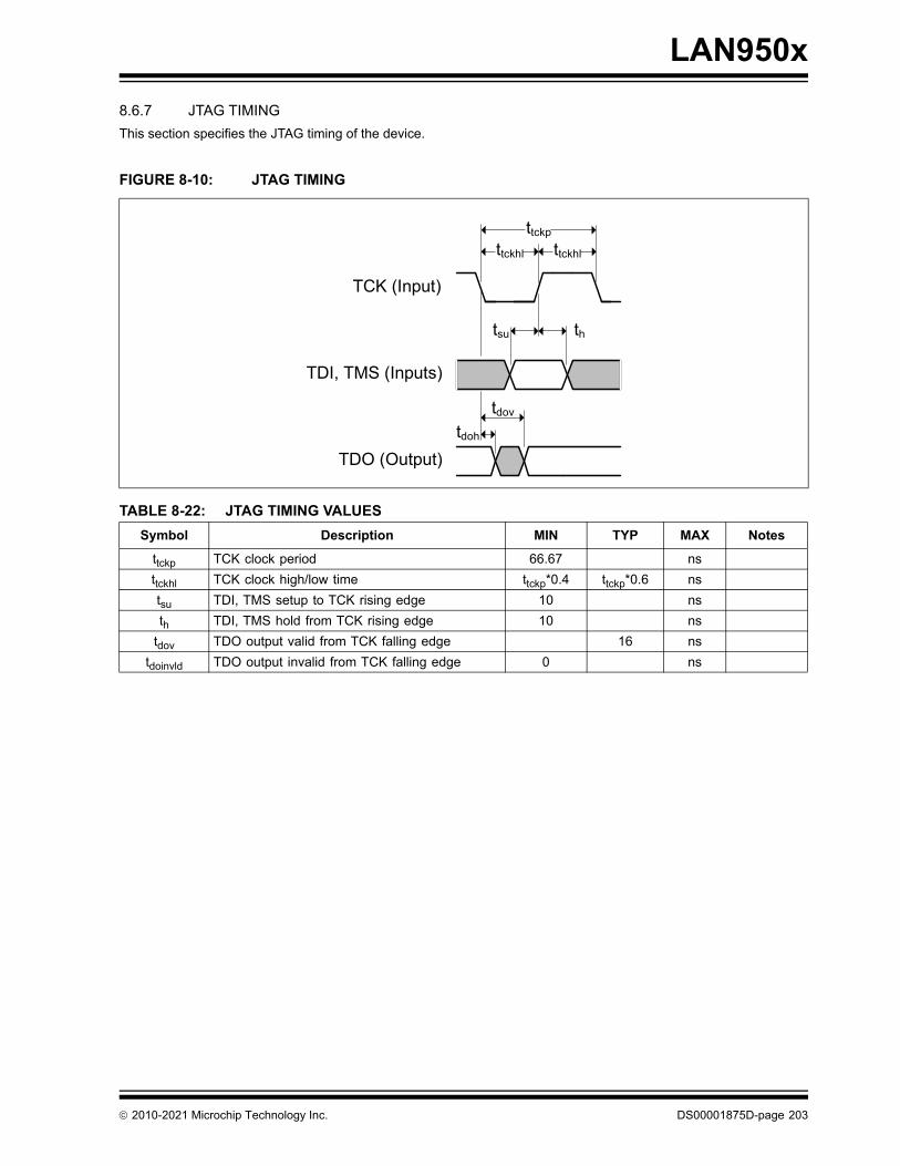
LAN950x
8.6.7 JTAG TIMING
This section specifies the JTAG timing of the device.
FIGURE 8-10: JTAG TIMING
TABLE 8-22: JTAG TIMING VALUES
Symbol Description MIN TYP MAX Notes
ttckp TCK clock period 66.67 ns
ttckhl TCK clock high/low time ttckp*0.4 ttckp*0.6 ns
tsu TDI, TMS setup to TCK rising edge 10 ns
th TDI, TMS hold from TCK rising edge 10 ns
tdov TDO output valid from TCK falling edge 16 ns
tdoinvld TDO output invalid from TCK falling edge 0 ns
TCK (Input)
TDI, TMS (Inputs)
ttckhl
ttckp
ttckhl
tsu th
tdov
TDO (Output)
tdoh
2010-2021 Microchip Technology Inc. DS00001875D-page 203
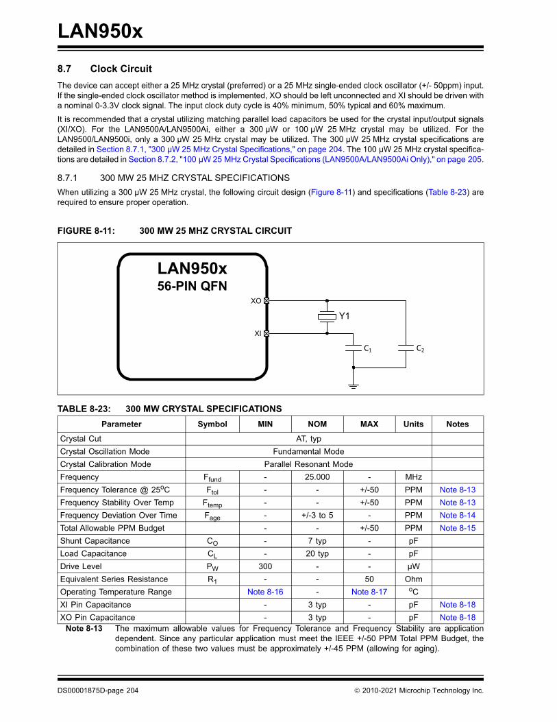
LAN950x
8.7 Clock Circuit
The device can accept either a 25 MHz crystal (preferred) or a 25 MHz single-ended clock oscillator (+/- 50ppm) input.If the single-ended clock oscillator method is implemented, XO should be left unconnected and XI should be driven witha nominal 0-3.3V clock signal. The input clock duty cycle is 40% minimum, 50% typical and 60% maximum.
It is recommended that a crystal utilizing matching parallel load capacitors be used for the crystal input/output signals(XI/XO). For the LAN9500A/LAN9500Ai, either a 300 µW or 100 µW 25 MHz crystal may be utilized. For theLAN9500/LAN9500i, only a 300 µW 25 MHz crystal may be utilized. The 300 µW 25 MHz crystal specifications aredetailed in Section 8.7.1, "300 µW 25 MHz Crystal Specifications," on page 204. The 100 µW 25 MHz crystal specifica-tions are detailed in Section 8.7.2, "100 µW 25 MHz Crystal Specifications (LAN9500A/LAN9500Ai Only)," on page 205.
8.7.1 300 ΜW 25 MHZ CRYSTAL SPECIFICATIONS
When utilizing a 300 µW 25 MHz crystal, the following circuit design (Figure 8-11) and specifications (Table 8-23) arerequired to ensure proper operation.
Note 8-13 The maximum allowable values for Frequency Tolerance and Frequency Stability are applicationdependent. Since any particular application must meet the IEEE +/-50 PPM Total PPM Budget, thecombination of these two values must be approximately +/-45 PPM (allowing for aging).
FIGURE 8-11: 300 ΜW 25 MHZ CRYSTAL CIRCUIT
TABLE 8-23: 300 ΜW CRYSTAL SPECIFICATIONS
Parameter Symbol MIN NOM MAX Units Notes
Crystal Cut AT, typ
Crystal Oscillation Mode Fundamental Mode
Crystal Calibration Mode Parallel Resonant Mode
Frequency Ffund - 25.000 - MHz
Frequency Tolerance @ 25oC Ftol - - +/-50 PPM Note 8-13
Frequency Stability Over Temp Ftemp - - +/-50 PPM Note 8-13
Frequency Deviation Over Time Fage - +/-3 to 5 - PPM Note 8-14
Total Allowable PPM Budget - - +/-50 PPM Note 8-15
Shunt Capacitance CO - 7 typ - pF
Load Capacitance CL - 20 typ - pF
Drive Level PW 300 - - µW
Equivalent Series Resistance R1 - - 50 Ohm
Operating Temperature Range Note 8-16 - Note 8-17 oC
XI Pin Capacitance - 3 typ - pF Note 8-18
XO Pin Capacitance - 3 typ - pF Note 8-18
LAN950x56-PIN QFN
XO
XI
Y1
C1 C2
DS00001875D-page 204 2010-2021 Microchip Technology Inc.
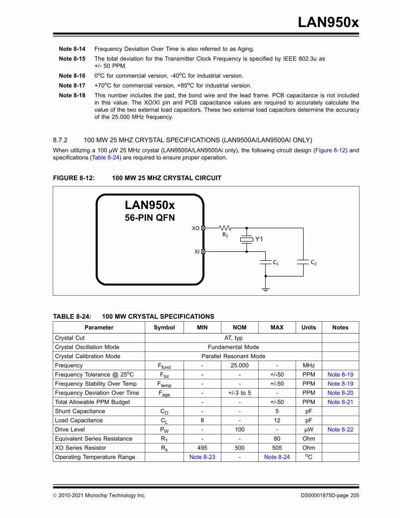
LAN950x
Note 8-14 Frequency Deviation Over Time is also referred to as Aging.
Note 8-15 The total deviation for the Transmitter Clock Frequency is specified by IEEE 802.3u as +/- 50 PPM.
Note 8-16 0oC for commercial version, -40oC for industrial version.
Note 8-17 +70oC for commercial version, +85oC for industrial version.
Note 8-18 This number includes the pad, the bond wire and the lead frame. PCB capacitance is not includedin this value. The XO/XI pin and PCB capacitance values are required to accurately calculate thevalue of the two external load capacitors. These two external load capacitors determine the accuracyof the 25.000 MHz frequency.
8.7.2 100 ΜW 25 MHZ CRYSTAL SPECIFICATIONS (LAN9500A/LAN9500AI ONLY)
When utilizing a 100 µW 25 MHz crystal (LAN9500A/LAN9500Ai only), the following circuit design (Figure 8-12) andspecifications (Table 8-24) are required to ensure proper operation.
FIGURE 8-12: 100 ΜW 25 MHZ CRYSTAL CIRCUIT
TABLE 8-24: 100 ΜW CRYSTAL SPECIFICATIONS
Parameter Symbol MIN NOM MAX Units Notes
Crystal Cut AT, typ
Crystal Oscillation Mode Fundamental Mode
Crystal Calibration Mode Parallel Resonant Mode
Frequency Ffund - 25.000 - MHz
Frequency Tolerance @ 25oC Ftol - - +/-50 PPM Note 8-19
Frequency Stability Over Temp Ftemp - - +/-50 PPM Note 8-19
Frequency Deviation Over Time Fage - +/-3 to 5 - PPM Note 8-20
Total Allowable PPM Budget - - +/-50 PPM Note 8-21
Shunt Capacitance CO - - 5 pF
Load Capacitance CL 8 - 12 pF
Drive Level PW - 100 - µW Note 8-22
Equivalent Series Resistance R1 - - 80 Ohm
XO Series Resistor Rs 495 500 505 Ohm
Operating Temperature Range Note 8-23 - Note 8-24 oC
LAN950x56-PIN QFN
XO
XI
RSY1
C1 C2
2010-2021 Microchip Technology Inc. DS00001875D-page 205
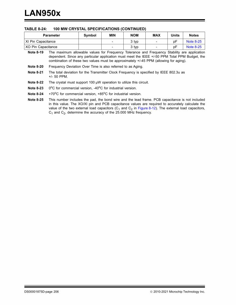
LAN950x
Note 8-19 The maximum allowable values for Frequency Tolerance and Frequency Stability are applicationdependent. Since any particular application must meet the IEEE +/-50 PPM Total PPM Budget, thecombination of these two values must be approximately +/-45 PPM (allowing for aging).
Note 8-20 Frequency Deviation Over Time is also referred to as Aging.
Note 8-21 The total deviation for the Transmitter Clock Frequency is specified by IEEE 802.3u as +/- 50 PPM.
Note 8-22 The crystal must support 100 µW operation to utilize this circuit.
Note 8-23 0oC for commercial version, -40oC for industrial version.
Note 8-24 +70oC for commercial version, +85oC for industrial version.
Note 8-25 This number includes the pad, the bond wire and the lead frame. PCB capacitance is not includedin this value. The XO/XI pin and PCB capacitance values are required to accurately calculate thevalue of the two external load capacitors (C1 and C2 in Figure 8-12). The external load capacitors,C1 and C2, determine the accuracy of the 25.000 MHz frequency.
XI Pin Capacitance - 3 typ - pF Note 8-25
XO Pin Capacitance - 3 typ - pF Note 8-25
TABLE 8-24: 100 ΜW CRYSTAL SPECIFICATIONS (CONTINUED)
Parameter Symbol MIN NOM MAX Units Notes
DS00001875D-page 206 2010-2021 Microchip Technology Inc.
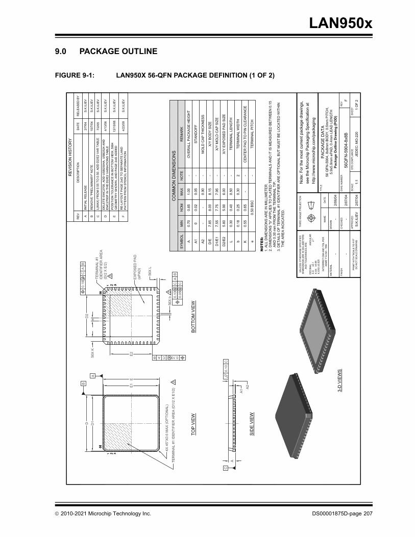
LAN950x
9.0 PACKAGE OUTLINE
FIGURE 9-1: LAN950X 56-QFN PACKAGE DEFINITION (1 OF 2)
Not
e: F
or th
e m
ost c
urre
nt p
acka
ge d
raw
ings
, se
e th
e M
icro
chip
Pac
kagi
ng S
peci
ficat
ion
at
http
://w
ww
.mic
roch
ip.c
om/p
acka
ging
2010-2021 Microchip Technology Inc. DS00001875D-page 207
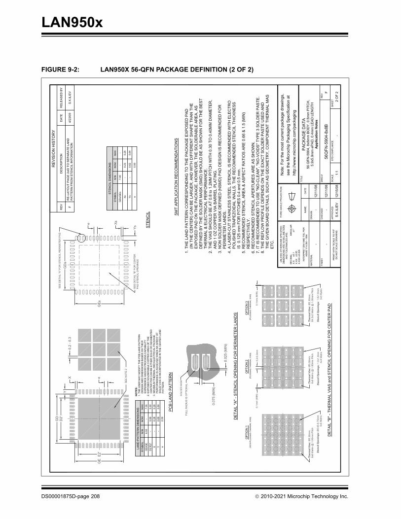
LAN950x
FIGURE 9-2: LAN950X 56-QFN PACKAGE DEFINITION (2 OF 2)
Not
e: F
or th
e m
ost c
urre
nt p
acka
ge d
raw
ings
, se
e th
e M
icro
chip
Pac
kagi
ng S
peci
ficat
ion
at
http
://w
ww
.mic
roch
ip.c
om/p
acka
ging
DS00001875D-page 208 2010-2021 Microchip Technology Inc.
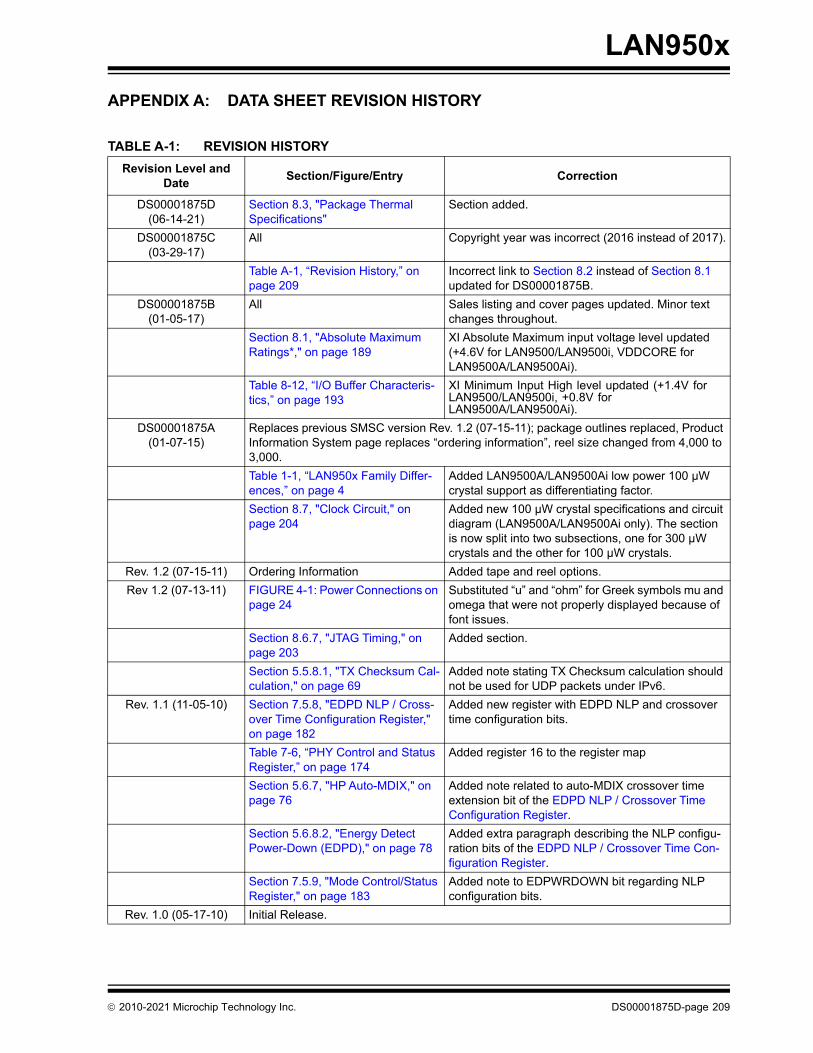
2010-2021 Microchip Technology Inc. DS00001875D-page 209
LAN950x
APPENDIX A: DATA SHEET REVISION HISTORY
TABLE A-1: REVISION HISTORY
Revision Level and Date
Section/Figure/Entry Correction
DS00001875D(06-14-21)
Section 8.3, "Package Thermal Specifications"
Section added.
DS00001875C(03-29-17)
All Copyright year was incorrect (2016 instead of 2017).
Table A-1, “Revision History,” on page 209
Incorrect link to Section 8.2 instead of Section 8.1 updated for DS00001875B.
DS00001875B(01-05-17)
All Sales listing and cover pages updated. Minor text changes throughout.
Section 8.1, "Absolute Maximum Ratings*," on page 189
XI Absolute Maximum input voltage level updated (+4.6V for LAN9500/LAN9500i, VDDCORE for LAN9500A/LAN9500Ai).
Table 8-12, “I/O Buffer Characteris-tics,” on page 193
XI Minimum Input High level updated (+1.4V for LAN9500/LAN9500i, +0.8V for LAN9500A/LAN9500Ai).
DS00001875A(01-07-15)
Replaces previous SMSC version Rev. 1.2 (07-15-11); package outlines replaced, Product Information System page replaces “ordering information”, reel size changed from 4,000 to 3,000.
Table 1-1, “LAN950x Family Differ-ences,” on page 4
Added LAN9500A/LAN9500Ai low power 100 µW crystal support as differentiating factor.
Section 8.7, "Clock Circuit," on page 204
Added new 100 µW crystal specifications and circuit diagram (LAN9500A/LAN9500Ai only). The section is now split into two subsections, one for 300 µW crystals and the other for 100 µW crystals.
Rev. 1.2 (07-15-11) Ordering Information Added tape and reel options.
Rev 1.2 (07-13-11) FIGURE 4-1: Power Connections on page 24
Substituted “u” and “ohm” for Greek symbols mu and omega that were not properly displayed because of font issues.
Section 8.6.7, "JTAG Timing," on page 203
Added section.
Section 5.5.8.1, "TX Checksum Cal-culation," on page 69
Added note stating TX Checksum calculation should not be used for UDP packets under IPv6.
Rev. 1.1 (11-05-10) Section 7.5.8, "EDPD NLP / Cross-over Time Configuration Register," on page 182
Added new register with EDPD NLP and crossover time configuration bits.
Table 7-6, “PHY Control and Status Register,” on page 174
Added register 16 to the register map
Section 5.6.7, "HP Auto-MDIX," on page 76
Added note related to auto-MDIX crossover time extension bit of the EDPD NLP / Crossover Time Configuration Register.
Section 5.6.8.2, "Energy Detect Power-Down (EDPD)," on page 78
Added extra paragraph describing the NLP configu-ration bits of the EDPD NLP / Crossover Time Con-figuration Register.
Section 7.5.9, "Mode Control/Status Register," on page 183
Added note to EDPWRDOWN bit regarding NLP configuration bits.
Rev. 1.0 (05-17-10) Initial Release.
DS00001875D-page 210 2010-2021 Microchip Technology Inc.
THE MICROCHIP WEB SITE
Microchip provides online support via our WWW site at www.microchip.com. This web site is used as a means to makefiles and information easily available to customers. Accessible by using your favorite Internet browser, the web sitecontains the following information:
• Product Support – Data sheets and errata, application notes and sample programs, design resources, user’s guides and hardware support documents, latest software releases and archived software
• General Technical Support – Frequently Asked Questions (FAQ), technical support requests, online discussion groups, Microchip consultant program member listing
• Business of Microchip – Product selector and ordering guides, latest Microchip press releases, listing of seminars and events, listings of Microchip sales offices, distributors and factory representatives
CUSTOMER CHANGE NOTIFICATION SERVICE
Microchip’s customer notification service helps keep customers current on Microchip products. Subscribers will receivee-mail notification whenever there are changes, updates, revisions or errata related to a specified product family ordevelopment tool of interest.
To register, access the Microchip web site at www.microchip.com. Under “Support”, click on “Customer Change Notifi-cation” and follow the registration instructions.
CUSTOMER SUPPORT
Users of Microchip products can receive assistance through several channels:
• Distributor or Representative
• Local Sales Office
• Field Application Engineer (FAE)
• Technical Support
Customers should contact their distributor, representative or Field Application Engineer (FAE) for support. Local salesoffices are also available to help customers. A listing of sales offices and locations is included in the back of thisdocument.
Technical support is available through the web site at: http://microchip.com/support
2010-2021 Microchip Technology Inc. DS00001875D-page 211
LAN950x
PRODUCT IDENTIFICATION SYSTEM
To order or obtain information, e.g., on pricing or delivery, refer to the factory or the listed sales office.
Device: LAN9500, LAN9500i, LAN9500A, LAN9500Ai
Temperature Range:
Blank = 0C to+70C (Extended Commercial)i = -40C to+85C (Industrial)
Package: ABZJ = 56-pin QFN (Tray)ABZJ-TR = 56-pin QFN (Tape & Reel)
Tape and Reel Option:
Blank = Standard packaging (tray)TR = Tape and Reel(1)
Examples:
a) LAN9500-ABZJ56-pin RoHS compliant packageExtended commercial temperature
b) LAN9500-ABZJ-TR56-pin RoHS compliant packageExtended commercial temperature
c) LAN9500i-ABZJ56-pin RoHS compliant packageIndustrial temperature
d) LAN9500i-ABZJ-TR56-pin RoHS compliant packageIndustrial temperature
e) LAN9500A-ABZJ56-pin RoHS compliant packageExtended commercial temperature
f) LAN9500A-ABZJ-TR56-pin RoHS compliant packageExtended commercial temperature
g) LAN9500Ai-ABZJ56-pin RoHS compliant packageIndustrial temperature
h) LAN9500Ai-ABZJ-TR56-pin RoHS compliant packageIndustrial temperature
Note 1: Tape and Reel identifier only appears in the catalog part number description. This identifier is used for ordering purposes and is not printed on the device package. Check with your Microchip Sales Office for package availability with the Tape and Reel option.Reel size is 3,000.
PART NO. [X] XXX
PackageTemperatureRange
Device
[X](1)
Tape and ReelOption
- -
LAN950X
DS
Note the following details of the code protection feature on Microchip devices:
• Microchip products meet the specifications contained in their particular Microchip Data Sheet.
• Microchip believes that its family of products is secure when used in the intended manner and under normal conditions.
• There are dishonest and possibly illegal methods being used in attempts to breach the code protection features of the Microchip devices. We believe that these methods require using the Microchip products in a manner outside the operating specifications contained in Microchip's Data Sheets. Attempts to breach these code protection features, most likely, cannot be accomplished without violating Microchip's intellectual property rights.
• Microchip is willing to work with any customer who is concerned about the integrity of its code.
• Neither Microchip nor any other semiconductor manufacturer can guarantee the security of its code. Code protection does not mean that we are guaranteeing the product is "unbreakable." Code protection is constantly evolving. We at Microchip are committed to continuously improving the code protection features of our products. Attempts to break Microchip's code protection feature may be a violation of the Digital Millennium Copyright Act. If such acts allow unauthorized access to your software or other copyrighted work, you may have a right to sue for relief under that Act.
Information contained in this publication is provided for the sole purpose of designing with and using Microchip products. Information regarding device applications and the like is provided only for your convenience and may be superseded by updates. It is your responsi-bility to ensure that your application meets with your specifications.
THIS INFORMATION IS PROVIDED BY MICROCHIP "AS IS". MICROCHIP MAKES NO REPRESENTATIONS OR WARRANTIES OF ANY KIND WHETHER EXPRESS OR IMPLIED, WRITTEN OR ORAL, STATUTORY OR OTHERWISE, RELATED TO THE INFORMA-TION INCLUDING BUT NOT LIMITED TO ANY IMPLIED WARRANTIES OF NON-INFRINGEMENT, MERCHANTABILITY, AND FIT-NESS FOR A PARTICULAR PURPOSE OR WARRANTIES RELATED TO ITS CONDITION, QUALITY, OR PERFORMANCE.
IN NO EVENT WILL MICROCHIP BE LIABLE FOR ANY INDIRECT, SPECIAL, PUNITIVE, INCIDENTAL OR CONSEQUENTIAL LOSS, DAMAGE, COST OR EXPENSE OF ANY KIND WHATSOEVER RELATED TO THE INFORMATION OR ITS USE, HOWEVER CAUSED, EVEN IF MICROCHIP HAS BEEN ADVISED OF THE POSSIBILITY OR THE DAMAGES ARE FORESEEABLE. TO THE FULLEST EXTENT ALLOWED BY LAW, MICROCHIP'S TOTAL LIABILITY ON ALL CLAIMS IN ANY WAY RELATED TO THE INFOR-MATION OR ITS USE WILL NOT EXCEED THE AMOUNT OF FEES, IF ANY, THAT YOU HAVE PAID DIRECTLY TO MICROCHIP FOR THE INFORMATION. Use of Microchip devices in life support and/or safety applications is entirely at the buyer's risk, and the buyer agrees to defend, indemnify and hold harmless Microchip from any and all damages, claims, suits, or expenses resulting from such use. No licenses are conveyed, implicitly or otherwise, under any Microchip intellectual property rights unless otherwise stated.
Trademarks
The Microchip name and logo, the Microchip logo, Adaptec, AnyRate, AVR, AVR logo, AVR Freaks, BesTime, BitCloud, chipKIT, chipKIT logo, CryptoMemory, CryptoRF, dsPIC, FlashFlex, flexPWR, HELDO, IGLOO, JukeBlox, KeeLoq, Kleer, LANCheck, LinkMD, maXStylus, maXTouch, MediaLB, megaAVR, Microsemi, Microsemi logo, MOST, MOST logo, MPLAB, OptoLyzer, PackeTime, PIC, picoPower, PICSTART, PIC32 logo, PolarFire, Prochip Designer, QTouch, SAM-BA, SenGenuity, SpyNIC, SST, SST Logo, SuperFlash, Symmetricom, SyncServer, Tachyon, TimeSource, tinyAVR, UNI/O, Vectron, and XMEGA are registered trademarks of Microchip Technology Incorporated in the U.S.A. and other countries.AgileSwitch, APT, ClockWorks, The Embedded Control Solutions Company, EtherSynch, FlashTec, Hyper Speed Control, HyperLight Load, IntelliMOS, Libero, motorBench, mTouch, Powermite 3, Precision Edge, ProASIC, ProASIC Plus, ProASIC Plus logo, Quiet-Wire, SmartFusion, SyncWorld, Temux, TimeCesium, TimeHub, TimePictra, TimeProvider, WinPath, and ZL are registered trademarks of Microchip Technology Incorporated in the U.S.A.
Adjacent Key Suppression, AKS, Analog-for-the-Digital Age, Any Capacitor, AnyIn, AnyOut, Augmented Switching, BlueSky, BodyCom, CodeGuard, CryptoAuthentication, CryptoAutomotive, CryptoCompanion, CryptoController, dsPICDEM, dsPICDEM.net, Dynamic Average Matching, DAM, ECAN, Espresso T1S, EtherGREEN, IdealBridge, In-Circuit Serial Programming, ICSP, INICnet, Intelligent Paralleling, Inter-Chip Connectivity, JitterBlocker, maxCrypto, maxView, memBrain, Mindi, MiWi, MPASM, MPF, MPLAB Certified logo, MPLIB, MPLINK, MultiTRAK, NetDetach, Omniscient Code Generation, PICDEM, PICDEM.net, PICkit, PICtail, PowerSmart, PureSilicon, QMatrix, REAL ICE, Ripple Blocker, RTAX, RTG4, SAM-ICE, Serial Quad I/O, simpleMAP, SimpliPHY, SmartBuffer, SMART-I.S., storClad, SQI, SuperSwitcher, SuperSwitcher II, Switchtec, SynchroPHY, Total Endurance, TSHARC, USBCheck, VariSense, VectorBlox, VeriPHY, ViewSpan, WiperLock, XpressConnect, and ZENA are trademarks of Microchip Technology Incorporated in the U.S.A. and other countries.
SQTP is a service mark of Microchip Technology Incorporated in the U.S.A.The Adaptec logo, Frequency on Demand, Silicon Storage Technology, and Symmcom are registered trademarks of Microchip Technology Inc. in other countries.
GestIC is a registered trademark of Microchip Technology Germany II GmbH & Co. KG, a subsidiary of Microchip Technology Inc., in other countries.
All other trademarks mentioned herein are property of their respective companies.
© 2010-2021, Microchip Technology Incorporated, All Rights Reserved.
ISBN: 9781522483564
For information regarding Microchip’s Quality Management Systems, please visit www.microchip.com/quality.
00001875D-page 212 2010-2021 Microchip Technology Inc.

DS00001875D-page 213 2010-2021 Microchip Technology Inc.
AMERICASCorporate Office2355 West Chandler Blvd.Chandler, AZ 85224-6199Tel: 480-792-7200 Fax: 480-792-7277Technical Support: http://www.microchip.com/supportWeb Address: www.microchip.com
AtlantaDuluth, GA Tel: 678-957-9614 Fax: 678-957-1455
Austin, TXTel: 512-257-3370
BostonWestborough, MA Tel: 774-760-0087 Fax: 774-760-0088
ChicagoItasca, IL Tel: 630-285-0071 Fax: 630-285-0075
DallasAddison, TX Tel: 972-818-7423 Fax: 972-818-2924
DetroitNovi, MI Tel: 248-848-4000
Houston, TX Tel: 281-894-5983
IndianapolisNoblesville, IN Tel: 317-773-8323Fax: 317-773-5453Tel: 317-536-2380
Los AngelesMission Viejo, CA Tel: 949-462-9523Fax: 949-462-9608Tel: 951-273-7800
Raleigh, NC Tel: 919-844-7510
New York, NY Tel: 631-435-6000
San Jose, CA Tel: 408-735-9110Tel: 408-436-4270
Canada - TorontoTel: 905-695-1980 Fax: 905-695-2078
ASIA/PACIFICAustralia - SydneyTel: 61-2-9868-6733
China - BeijingTel: 86-10-8569-7000
China - ChengduTel: 86-28-8665-5511
China - ChongqingTel: 86-23-8980-9588
China - DongguanTel: 86-769-8702-9880
China - GuangzhouTel: 86-20-8755-8029
China - HangzhouTel: 86-571-8792-8115
China - Hong Kong SARTel: 852-2943-5100
China - NanjingTel: 86-25-8473-2460
China - QingdaoTel: 86-532-8502-7355
China - ShanghaiTel: 86-21-3326-8000
China - ShenyangTel: 86-24-2334-2829
China - ShenzhenTel: 86-755-8864-2200
China - SuzhouTel: 86-186-6233-1526
China - WuhanTel: 86-27-5980-5300
China - XianTel: 86-29-8833-7252
China - XiamenTel: 86-592-2388138
China - ZhuhaiTel: 86-756-3210040
ASIA/PACIFICIndia - BangaloreTel: 91-80-3090-4444
India - New DelhiTel: 91-11-4160-8631
India - PuneTel: 91-20-4121-0141
Japan - OsakaTel: 81-6-6152-7160
Japan - TokyoTel: 81-3-6880- 3770
Korea - DaeguTel: 82-53-744-4301
Korea - SeoulTel: 82-2-554-7200
Malaysia - Kuala LumpurTel: 60-3-7651-7906
Malaysia - PenangTel: 60-4-227-8870
Philippines - ManilaTel: 63-2-634-9065
SingaporeTel: 65-6334-8870
Taiwan - Hsin ChuTel: 886-3-577-8366
Taiwan - KaohsiungTel: 886-7-213-7830
Taiwan - TaipeiTel: 886-2-2508-8600
Thailand - BangkokTel: 66-2-694-1351
Vietnam - Ho Chi MinhTel: 84-28-5448-2100
EUROPEAustria - WelsTel: 43-7242-2244-39Fax: 43-7242-2244-393
Denmark - CopenhagenTel: 45-4485-5910 Fax: 45-4485-2829
Finland - EspooTel: 358-9-4520-820
France - ParisTel: 33-1-69-53-63-20 Fax: 33-1-69-30-90-79
Germany - GarchingTel: 49-8931-9700
Germany - HaanTel: 49-2129-3766400
Germany - HeilbronnTel: 49-7131-72400
Germany - KarlsruheTel: 49-721-625370
Germany - MunichTel: 49-89-627-144-0 Fax: 49-89-627-144-44
Germany - RosenheimTel: 49-8031-354-560
Israel - Ra’anana Tel: 972-9-744-7705
Italy - Milan Tel: 39-0331-742611 Fax: 39-0331-466781
Italy - PadovaTel: 39-049-7625286
Netherlands - DrunenTel: 31-416-690399 Fax: 31-416-690340
Norway - TrondheimTel: 47-7288-4388
Poland - WarsawTel: 48-22-3325737
Romania - BucharestTel: 40-21-407-87-50
Spain - MadridTel: 34-91-708-08-90Fax: 34-91-708-08-91
Sweden - GothenbergTel: 46-31-704-60-40
Sweden - StockholmTel: 46-8-5090-4654
UK - WokinghamTel: 44-118-921-5800Fax: 44-118-921-5820
Worldwide Sales and Service
02/28/20