Lab1 Appendix.pdf
52
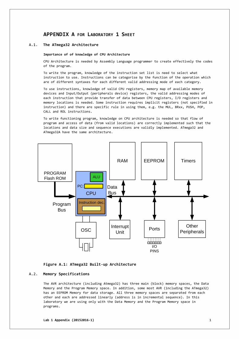
Lab 1 Appendix (20152016-1) 1 APPENDIX A FOR LABORATORY 1 SHEET The ATmega32 Architecture A.1. Importance of of knowledge of CPU Architecture CPU Architecture is needed by Assembly Language programmer to create effectively the codes of the program. To write the program, knowledge of the instruction set list is need to select what instruction to use. Instructions can be categorise by the function of the operation which are of different syntaxes for each different valid addressing mode of each category. To use instructions, knowledge of valid CPU registers, memory map of available memory devices and Input/Output (peripherals device) registers, the valid addressing modes of each instruction that provide transfer of data between CPU registers, I/O registers and memory locations is needed. Some instruction requires implicit registers (not specified in instruction) and there are specific rule in using them, e.g. the MUL, BRxx, PUSH, POP, CALL and ROL instructions. To write functioning program, knowledge on CPU architecture is needed so that flow of program and access of data (from valid locations) are correctly implemented such that the locations and data size and sequence executions are validly implemented. ATmega32 and ATmega32A have the same architecture. Figure A.1: ATmega32 Built-up Architecture Memory Specifications A.2. The AVR architecture (including Atmega32) has three main (block) memory spaces, the Data Memory and the Program Memory space. In addition, some most AVR (including the ATmega32) has an EEPROM Memory for data storage. All three memory spaces are separated from each other and each are addressed linearly (address is in incremental sequence). In this laboratory we are using only with the Data Memory and the Program Memory space in programs. PROGRAM Flash ROM Ports OSC CPU Timers Other Peripherals Program Bus Data Bus RAM I/O PINS EEPROM Interrupt Unit ALU PC: Instruction dec.
-
Upload
fishy-kenny -
Category
Documents
-
view
280 -
download
0
Transcript of Lab1 Appendix.pdf
Lab 1 Appendix (20152016-1) 1
APPENDIX A FOR LABORATORY 1 SHEET
The ATmega32 Architecture A.1.
Importance of of knowledge of CPU Architecture
CPU Architecture is needed by Assembly Language programmer to create effectively the codes
of the program.
To write the program, knowledge of the instruction set list is need to select what
instruction to use. Instructions can be categorise by the function of the operation which
are of different syntaxes for each different valid addressing mode of each category.
To use instructions, knowledge of valid CPU registers, memory map of available memory
devices and Input/Output (peripherals device) registers, the valid addressing modes of
each instruction that provide transfer of data between CPU registers, I/O registers and
memory locations is needed. Some instruction requires implicit registers (not specified in
instruction) and there are specific rule in using them, e.g. the MUL, BRxx, PUSH, POP,
CALL and ROL instructions.
To write functioning program, knowledge on CPU architecture is needed so that flow of
program and access of data (from valid locations) are correctly implemented such that the
locations and data size and sequence executions are validly implemented. ATmega32 and
ATmega32A have the same architecture.
Figure A.1: ATmega32 Built-up Architecture
Memory Specifications A.2.
The AVR architecture (including Atmega32) has three main (block) memory spaces, the Data
Memory and the Program Memory space. In addition, some most AVR (including the ATmega32)
has an EEPROM Memory for data storage. All three memory spaces are separated from each
other and each are addressed linearly (address is in incremental sequence). In this
laboratory we are using only with the Data Memory and the Program Memory space in
programs.
PROGRAM
Flash ROM
PortsOSC
CPU
Timers
Other
Peripherals
Program
Bus
Data
Bus
RAM
I/O
PINS
EEPROM
Interrupt
Unit
ALU
PC:
Instruction dec.

Lab 1 Appendix (20152016-1) 2
Memory Map
The memory map of a microcontroller is a diagram which gives the size, type and layout of
the memories that are available in the microcontroller. The information use to construct
the memory map is extracted from the datasheet of the microcontroller.
The diagram below gives the memory map for three (3) blocks of memory spaces of
the ATMega32.
Figure A.3: ATmega32 (ATmega32A) Memory map
Program Memory A.3.
The Atmega32 contains 32K (32768) bytes of On-chip In-System Reprogrammable Flash memory
for program storage. For software security, the Flash Program memory space is divided into
two sections, Boot Program section and Application Program section. The figure below
illustrates the Flash Memory.
a. Instruction in Program Memory
The Atmega32 instructions are 16 wide: when accessed by the CPU (using Program
Counter) to address instruction, the Flash is organized as 16K x 16. Each addressed
hold 2 bytes of data. The two bytes of each address are arranged in “little endian”
order.
b. Data in Program Memory
The Flash memory can also be used to store data (thus is non-volatile – data not lost
when power is removed).
When accessed by the CPU (using Pointer Register Z), the Flash is organized as 32K x
8. Each addressed hold 1 bytes of data. So the absolute address to accessed byte size
data is calculated by multiplying 2 with the physical Flash memory address: the lower
byte of the word is the added with 1 (odd address).

Lab 1 Appendix (20152016-1) 3
Figure A.3: Addressing 16 bit data and 8 bit data of the Program Memory.
In this lab we will not access the Boot Program (Flash) section.
Program will be stored in the Application Program section (which is physically a flash
RAM) and data can be stored Program memory Space (Flash RAM) and Data memory Space (which
is physically a Static RAM or SRAM).
In real application the address location 0x00 to 0x29 should be reserved for interrupt
vector table as shown below.
High Byte Low Byte
15 14 13 12 11 10 9 8 7 6 5 4 3 2 1 0 7 6 5 4 3 2 1 0
$0000 Byte 0 Byte 1 $0000 Byte 0
$0001 Byte 2 Byte 3 $0001 Byte 1
$0002 Byte 4 Byte 5 $0002 Byte 2
$0003 Byte 3
$0004 Byte 4
$0005 Byte 5
$0006
$3FFE Byte 32764 Byte 32765
$3FFF Byte 32766 Byte 32767
$7FFC Byte 32764
$7FFD Byte 32765
$7FFE Byte 32767
$7FFF Byte 32766
Addressing 16 bit Data Addressing 8 bit Data
Address of 8-bi t data = Address of 16-
bit data * 2 or Shi ft left va lue of
address or (addr <<1). The high byte
wi l l take the even address (+0) and the
high byte wi l l take the odd address
(+1)
Only LPM and SPM instructions can be used used to access the program
memory
Lab 1 Appendix (20152016-1) 4
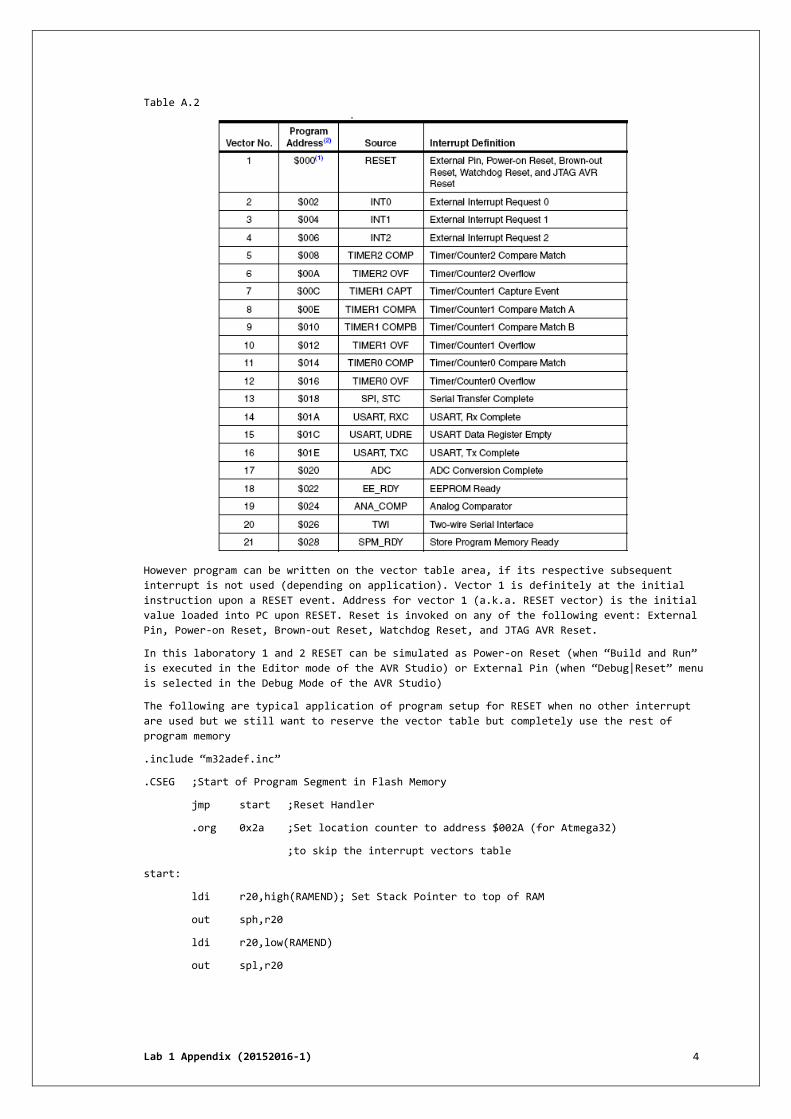
Table A.2
However program can be written on the vector table area, if its respective subsequent
interrupt is not used (depending on application). Vector 1 is definitely at the initial
instruction upon a RESET event. Address for vector 1 (a.k.a. RESET vector) is the initial
value loaded into PC upon RESET. Reset is invoked on any of the following event: External
Pin, Power-on Reset, Brown-out Reset, Watchdog Reset, and JTAG AVR Reset.
In this laboratory 1 and 2 RESET can be simulated as Power-on Reset (when “Build and Run”
is executed in the Editor mode of the AVR Studio) or External Pin (when “Debug|Reset” menu
is selected in the Debug Mode of the AVR Studio)
The following are typical application of program setup for RESET when no other interrupt
are used but we still want to reserve the vector table but completely use the rest of
program memory
.include “m32adef.inc”
.CSEG ;Start of Program Segment in Flash Memory
jmp start ;Reset Handler
.org 0x2a ;Set location counter to address $002A (for Atmega32)
;to skip the interrupt vectors table
start:
ldi r20,high(RAMEND); Set Stack Pointer to top of RAM
out sph,r20
ldi r20,low(RAMEND)
out spl,r20

Lab 1 Appendix (20152016-1) 5
Data (SRAM) Memory Space A.4.
Figure A.4 (1)
Figure A.4 (2)
There are three types of registers mapped in the Data (SRAM) Memory Space.
General Purpose Registers (GPR)
Standard I/O Registers
General Purpose RAM (Data Address Space)
The first of the SRAM is reserved for General Purpose Registers in the ATmega32. These registers are connected to the ALU (Arithmetic Logic Unit) and are used to manipulate data. The registers are labelled R0 – R31. The Register is divided into two group call Lower Registers and Upper Registers.
$0000
$0001
$0020
General
purpose
RAM
(SRAM)
R0
R1
R2
$001F
$005F
R31
...
TWBR
TWSR
SPH
SREG
...
General
Purpose
Registers
Standard I/O
Registers
$00
$01
$3E
$3F
$0060
...
...
Data Address
Space
I/O Address
...
8 bit
$FFFF
Lab 1 Appendix (20152016-1) 6
General Purpose Registers (GPR) Mappings A.5.
The GPRs and I/O Registers are mapped sequentially from address $0000 to address $005F in the Data Memory which is the RAM memory space. The mapping of each respective register is as in shown Figure A.4 (2).
The lower 16 registers, R0 – R15, work just the rest of the registers with the exception
of loading immediate data. These registers have access to the full range of the Data
Memory, ALU, and additional peripherals.
The upper 16 registers, R16 – R31, have additional capabilities. They have access to
immediate data using the LDI instruction. These registers will be the ones that get the
most use throughout your program. To move data into or out of these registers, the various
different Load and Store instructions are needed. All arithmetic instructions work on
these registers.
In normal case, to access these registers you use Register Direct Addressing mode (Section
A.6(b) though you can use Data Memory Addressing Mode(Section A.6(c)
a. I/O Registers Location
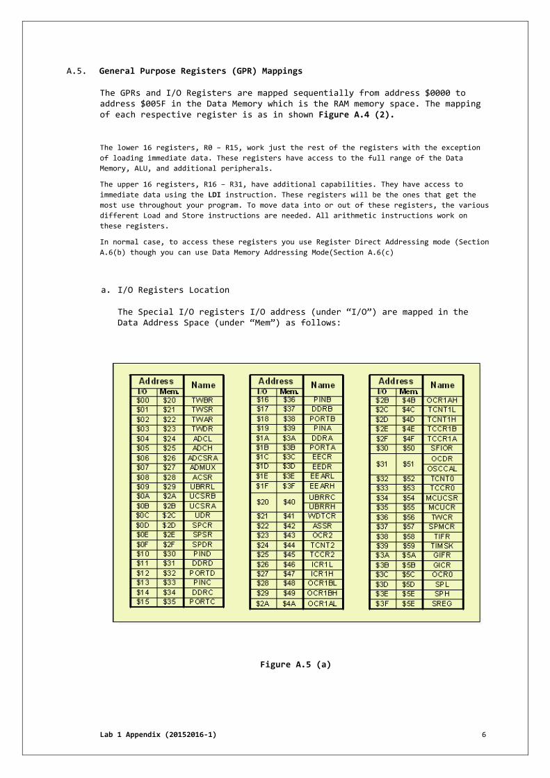
The Special I/O registers I/O address (under “I/O”) are mapped in the Data Address Space (under “Mem”) as follows:
Figure A.5 (a)

Lab 1 Appendix (20152016-1) 7
b. I/O Registers
These are Special Function Registers are registers in the ATmega32 that either control or monitor the various components of the chip. Most of the Special Function Registers have
read/write capabilities; check the datasheet for the ATmega32 for more details. These
register reside in the ATmega32 I/O Memory and as such, require the IN and OUT
instructions to read and write to these registers.
The ATmega32 is equipped with 4 Digital I/O Ports labelled Port A through Port D. Each
port has its own unique capabilities such as External RAM Addressing, PWMs, Timers, and
Counters. Unfortunately, this document will only cover the basics that are common with
each port. Digital I/O register will be used in Laboratory 2 thus explained more in
Laboratory 2.
In normal case, to access these registers you use Register Direct Addressing mode (Section
A.6(d) though you can use Data Memory Addressing Mode(Section A.6(c).
c. Internal SRAM (Data Memory)
The memory space is addressed from 0x60 to 0x085f. To access these memory spaces you must
use any of the five different addressing modes for the data memory cover: Direct, Indirect
with Displacement, Indirect, Indirect with Pre-decrement, Indirect with Post-increment. In
the General Purpose Register file, registers R26 to R31 feature the indirect addressing
pointer registers (X, Y, and Z).
To access Data memory locations, you must use Data Memory Addressing Mode(Section A.6(c).
Processor registers A.6.
In addition to these 32 general-purpose registers, the CPU has a few special-purpose
registers:
PC: 16-bit program counter
SP: 16-bit stack pointer
SREG: 8-bit status register
X, Y, and Z pointer registers: 8-bit segment registers that are prepended to 16-
bit addresses.
a. Program Counter
The Program Counter (PC) is a register that is apart of all central processing unit (CPU) or microprocessor. All microcontrollers contains a microprocessor and thus has a program counter. The purpose of the program counter is to hold/store (to point to) the address of the next instruction to be executed by the microcontroller's microprocessor.
The PC is automatically incremented to hold/store (to point to) the address of the
next instruction after execution of the current instruction.
When the program begins, the PC must contain the address of the first instruction in
the program which is the RESET event.
When a RESET event occurs The content of the reset vector is loaded into PC. A JMP
instruction at the reset vector address can be set to jump the bootloader program
starts.
Program instructions are stored in consecutive program memory locations. To jump
elsewhere in the program, Program Flow Control (branch/jump/call/return) instruction
is used.
Note: These are jump instructions that can modify the PC (e.g., the PC must change
when calling or returning from some other routine).
The CPU clock determines the execution time of instructions which a series of
execution can be calculated to generate a required delay.

Lab 1 Appendix (20152016-1) 8
b. The AVR Stack Pointer
The AVR ATmega32 stack pointer (SP) consist of two I/O register SPL (Stack Pointer Low) and SPH (Stack Pointer High). The size of the stack pointer depends on the amount of the ATmega32 data memory. The stack pointer is 16-bits wide but is accessed through
the two register, SPH:SPL. Stack Pointer points to the location where the next data
can be stored in the CPU stack. CALL, RCALL, PUSH and POP instructions uses and modify
the Stack Pointer when executed.
Figure A.5 (b)
c. Status Register (SREG)
The Status Register or SREG contains the important information about the ALU such as the
Carry Bit, Overflow Bit, and Zero Bit. These bits are set and cleared during ALU
instructions. This register becomes extremely useful during branching operations. The
following table details the bit assignments within the SREG.
Figure A.5 (c)
Status Register are:
Is 8 bits wide.
Contains information associated with the results of the most recent ALU operation.
Carry flag (C) set if CY from most signficant bit (MSB) or a borrow occur
on subtracts.
Often used when adding numbers that are larger than 8 bits. Here we
need to use an add with carry instruction (ADC) to add the next most significant byte.
Zero flag (Z) set if result is zero.
BREQ instruction says branch if zero flag is set. BRNE instruction says branch if zero flag is not set.

Lab 1 Appendix (20152016-1) 9
Negative flag (N) set if MSB is one. A copy of the most significant bit of
an arithmetic result.
Arithmetic instructions change the flags
Data transfer instructions do not change the flag.
The instruction set documentation identifies which flags each
instruction may modify.
Overflow flag (V) set if 2's complement overflow occurs.
An overflow occurs if you get the wrong sign for your result, e.g.,
6410 + 6410 = -12810 (010000002 + 010000002 = 100000002). Note: whenever the carry into the MSB and the carry out don't
match, we have an overflow.
Sign bit (S) s = N EXOR V, and shows the true sign of a comparison.
Half carry flag (H) is set when carry occurs from b3 to b4. Used with binary coded decimal (BCD) arithemtic. This is an
internal carry from additions.
T Bit copy. Special bit load and bit store instructions use this
bit.
I Interrupt flag. Set when interrupts are enabled.
d. The Pointer Registers: X, Y and Z-Registers
The last six of the General Purpose Registers have additional functionality. They serve as the pointers for indirect addressing. The ATmega32 has a 16-bit addressing scheme that requires two registers for the address alone. The AVR RISC structure supports this scheme with the X, Y, and Z-Registers. These registers are the last six General Purpose Registers (R26-R31). The following table details the register assignments:
Figure A.5 (d)
Addressing Modes A.7.
An addressing mode specifies how to determine/calculate the effective memory address of an
operand by using information held in registers and/or constants contained within an
instruction or elsewhere.
Instruction formats are of 3 types:
Implicit: No operand specified in the instruction, but the instruction execute a
defined function on one or more of a defined GPRs, Pointer Registers, CPU register or
Memory location.
E.g. NOP and RET
Single Operand: E.g. INC R0
Two operand: “LDI R16,0x20”, “STS 0x200,R0” and “MOV R0,R20”.

Lab 1 Appendix (20152016-1) 10
Operand can be of a constant or variable.
There are four types of variables that can be declared as operand: GPRs, I/O registers,
Data SRAM (GPRs, I/O registers and Data Memory are mapped in here too) and program Memory.
Each of these devices are accessed by each specific individual mode. As for GPRs and I/O
registers, though the have the own individual mode, the can be accessed by using the Data
Memory Addressing mode because they are mapped in the Data Memory space.
Addressing mode define the operand of the instruction (Refer section A.7) and for each
operand, there is a specific instruction that that is defined to use each of these
individual modes. All addressing mode is instruction specific which can be identified by
their operands specification in the Instruction Set Summary (Section A.7)
a. Immediate Addressing Mode
The Immediate addressing mode is only valid as source operand (mandatory) only and is
a constant. The destination operand must be of any the upper 16 GPRs (R16 thru R31).
E.g “LDI R16,0x30” or “CPI R31,3”
Where:
Source is an 8 bit constant that taken as the data.
Immediate addressing mode can be identified by the operands “Rd,K” and “Rdl,K”.
b. GPRs Addressing mode
There are two modes:
(a) Register Direct or Single Register Rd (Single operand or Implicit Operand
Instructions)
E.g. “INC R0”
Single Register addressing mode can be identified by the operands “Rd”.
(b) Register Direct, Two Registers Rd and Rr (Two Operand Instructions)
E.g. “MOV R0,R16”
Register addressing mode can be identified by the operands “Rd,R”.
c. Data Memory Addressing Modes
There five different addressing modes for the data memory:
1. Direct or Data Direct
Direct addressing mode can be identified by the operands “Rd,k” or “k,Rr” which
are used in instruction “LDS” and “STS” respectively.
“k” is taken as the absolute address where data can be taken from (for “LDS Rd,k”
instruction), or written to (for “STS k,Rr” instruction).
2. Indirect
Indirect addressing mode can be identified by the operands “Rd,X”, “Rd,Y”, “Rd,Z”,
“X,Rr”, “Y,Rr” or “Z,Rr” which are used either in instruction “LD” and “ST” only.
X, Y and Z are pointer registers
The content of the specified pointer register in the instruction is taken as the
address where data can be taken from (for “LD” instruction), or written to (for
“STD” instruction).
3. Indirect with Displacement
Indirect with Displacement addressing mode can be identified by the operands
“Rd,X+q”, “Rd,Y+q”, “Rd,Z+q”, “X+q,Rr”, “Y+q,Rr” or “Z+q,Rr” which are used either
in instruction “LDD” and “STD” only. X, Y and Z are pointer registers

Lab 1 Appendix (20152016-1) 11
The content of the specified pointer register in the instruction after being added
with q, is taken as the address where data can be taken from (for “LDD”
instruction), or written to (for “STD” instruction).
4. Indirect with Pre-decrement
Indirect with Pre-decrement addressing mode can be identified by the operands “-
X,Rr”, “-Y,Rr” or “-Z,Rr” which are used either in instruction “ST” only. X, Y and
Z are pointer registers
The content of the specified pointer register in the instruction after being
decremented by 1, is taken as the address where data taken from Rr can be written
to (for “ST” instruction).
5. Indirect with Post-increment.
Indirect with Post-increment addressing mode can be identified by the operands
“Rd,X+”, “Rd,Y+” or “Rd,Z+” which are used either in instruction “LD” only. X, Y
and Z are pointer registers
The content of the specified pointer register in the instruction is taken as the
address where data can be taken from (for “LD” instruction) to be written to Rd.
After the transfer the pointer register will be incremented by 1.
In the Register File, registers R26 to R31 feature the indirect Addressing Pointer
Registers.
The direct addressing reaches the entire data space.
The Indirect with Displacement mode reaches 63 address locations from the base
address given by the X, Y or Z register.
All instructions that use Data Memory Addressing Modes take two operands and one
of the operand must be a GPR.
When using indirect addressing modes with pre-decrement and post-increment, the
address registers X, Y, and Z are decremented or incremented by the execution of
the instruction.
The 32 general purpose working registers, 64 I/O Registers, and the 2048 bytes of
internal data SRAM in the ATmega32 are all accessible through all these addressing
modes
d. I/O Memory Addressing Modes
The I/O locations are accessed by the IN and OUT instructions, transferring data
between the 32 general purpose working registers and the I/O space.
I/O Registers within the address range $00 - $1F are directly bit accessible using the
SBI and CBI instructions. These addresses are Equates to labels in m32def.inc. The
valid names are given in Figure A.4(3).
In these registers, the value of single bits can be checked by using the SBIS and SBIC
instructions. Refer to the Instruction Set section for more details.
When using the I/O specific commands IN and OUT, the I/O addresses $00 - $3F must be
used.
When addressing I/O Registers as data space using LD and ST instructions, $20 must be
added to these addresses.
All instructions that uses I/O Memory Addressing Modes takes two operands, and one of
the operand must be a Register Direct Addressing Modes.
e. Program Memory Addressing mode
There are three modes:
(a) Program Memory Constant Addressing using the LPM and SPM Instructions
(b) Program Memory with Post-increment using the LPM Z+ Instruction

Lab 1 Appendix (20152016-1) 12
f. Direct Program Addressing Mode
The operand in JMP and CALL instruction is Direct Program Addressing. E.g. JMP k and
CALL k.
PC k
g. Indirect Program Addressing Mode
The implicit operands in IJMP and ICALL Indirect Program Addressing. These instruction
have no operands.
The source operand is the Z register and the destination operand is the PC (Program
Counter).
PC Z
h. Relative Program Addressing Mode
The operand in RJMP and RCALL instruction is Relative Program Addressing.
E.g. BRNE k, RJMP k, and RCALL k
There is only one operand which is the source operand and is a 12-bit constant. The
destination operand is implicit and it is the PC (Program Counter).
PC PC + 1 + k
AVR Instructions SET A.8.
Instructions of a processor when executed determine what task the processor should do. A
group of instructions which is arranged to perform a certain algorithm becomes a useful
program. Instruction must be written according to its format following its hardware design
which is specified in the processors in the instruction set reference manual. The
references for the AVR 8-bit microcontroller is in file “Atmel AVR 8-bit Instruction Set
manual 2014.pdf” (but refer to “Atmega32 Reference manual.pdf” pp 329 – 331 for list of
instruction supported on ATmega32/ATmega32A), which is categorised as below:
1. Arithmetic and Logic Operation Instructions
2. Data Transfer Instructions
3. Bit and Bit Test manipulation Instructions
4. Branch instructions a.k.a. Program Flow Control Instructions

Lab 1 Appendix (20152016-1) 13
a. Arithmetic and Logic Operation Instructions
Instruction from this category allows 8-bit arithmetic or logic operation on a GPR
(the destination operand). Instructions are specific for source operand which can be
either Immediate (a constant) or Register Direct. Result from instruction in this
category is stored in Status Register (either of the H, S, C, V and Z flag) can be
used by the conditional Branch Instruction to determine the flow of a program.
Table A8(a): Arithmetic and Logic Operation Instructions
b. Data Transfer Instructions
Except for LDI Instruction, instruction from this category allows transfer of 8-bit
data between GPRs and Data Memory, I/O Memory or Program Memory. If data need to me
transferred between Data Memory, I/O Memory or Program Memory, a GPR has to be used as
the intermediate storage to implement the transfer.

Lab 1 Appendix (20152016-1) 14
Table A8(b): Data Transfer Instructions

Lab 1 Appendix (20152016-1) 15
c. Bit and Bit Test manipulation Instructions
Instruction from this category allows specified bits of an 8-bit Number on a GPR or
the Status Register (the destination operand) to be changed or tested. Result from
instruction in this category is stored in Status Register (either of the H, S, C, V
and Z flag) can be used by the conditional Branch Instruction to determine the flow of
a program.
Table A8(b): Bit and Bit Test manipulation Instructions

Lab 1 Appendix (20152016-1) 16
d. Branch instructions (Program Flow Control Instructions)
Instruction from this category when executed, changes the Program Counter, either
conditional or unconditional thus allowing a program to executes with a decision
whether to jump or not. By using proper decision making in the codes, structured
block (IF, IF-Then-Else, While Loop, Do-While loop, For Loop, Repeat Loop and Switch-
Case) can be implemented.
Table A8(d): Branch instructions (Program Flow Control Instructions)

Lab 1 Appendix (20152016-1) 17
e. Instruction Format
The Instruction format of an ATmega32 microcontroller is specified in Instruction Set
Summary (refer Section A.7). The Instruction must have an Opword specified from the
Instruction Set’s Mnemonics and may be followed with one of the following operand
specification depending on the Opword:
1) No Operand (Example Instruction’s Opword Mnemonics: NOP, CLC)
2) One Operand (Example Instruction’s Opword Mnemonics: CLR R0, INC R1, JMP here)
Depending on the instruction the operand may be the:
a. The destination
b. The source and destination operand.
c. Source to an implicit destination
3) Two Operand (Example Instruction’s Opword Mnemonics: MOV, LDI, STS)
The valid source and destination operand is determined from the Instruction’s Opword
specified in Instruction Set Summary (refer Section A.7)
In this Laboratory, we will not use all but only some basic instruction which will be
used to help us understand a few of the Addressing Modes for the ATmega32
microcontroller.

Lab 1 Appendix (20152016-1) 18
Basic Assembler Directive A.9.
The Assembler supports a number of directives. The directives are not translated directly
into opcodes. Instead, they are used to adjust the location of the program in memory,
define macros, or initialize memory and so on.
Assembler-Directives control the assembler, they don't create any own code. The leading
dot must be in column 1 of the line. An overview of the basic directives is given in the
following table.
Table A9(d): Basic Assembler Directive
Segment Directive Description
Header
.DEVICE Defines the type of the target processor and the applicable set of instructions (illegal instructions for that type trigger an error message, syntax: .DEVICE AT90S8515)
.DEF Defines a synonym for a register (e.g. .DEF MyReg = R16)
.EQU Defines a symbol and sets its value (later changes of this value remain possible, syntax: .EQU test = 1234567, internal storage of the value is 4-byte- Integer)
.SET Fixes the value of a symbole (later redefinition is not possible)
.INCLUDE Includes a file and assembles its content, just like its content would be part of the calling file (typical e.g. including the header file for device ATmega32: .INCLUDE "m32Adefdef.inc")
Code
.CSEG Start of the code segment. All valid declaration using “.DB” and “.DW” only that follows is assembled to the code segment and will be stored the program memory space(Flash Memory).
.DB
Inserts one or more constant bytes in the code segment (could be numbers from 0..255, an ASCII-character like 'c', a string like 'abcde' or a combination like 1,2,3,'abc'. The number of inserted bytes must be even, otherwise an additional zero byte will be inserted by the assembler.)
.DW Insert a binary word in the code segment (e.g. produces a table within the code)
.LISTMAC Macros will be listed in the .LST-file. (Default is that macros are not listed)
.MACRO Beginning of a macro (no code will be produced, call of the macro later produces code, syntax: .MACRO macroname parameters, calling by: macroname parameters)
.ENDMACRO End of the macro
EEPROM
.ESEG Assemble to the EEPROM-segment (the code produced will go to the EEPROM section, the code produces an .EEP-file)
.DB Inserts one or more constant bytes in the EEPROM segment (could be numbers from 0..255, an ASCII-character like 'c', a string like 'abcde' or a combination like 1,2,3,'abc'.)
.DW Inserts a binary word to the EEPROM segment (the lower byte goes to the next adress, the higher byte follows on the incremented address)
SRAM
.DSEG
Assemble to the data segment (here only .BYTE directives and labels are valid, during assembly only the labels are used). All valid declaration that follows is assembled to the data segment and will be stored the DATA memory space(SRAM)
.BYTE Reserves one or more bytes space in the data segment (only used to produce correct labels, does not insert any values!)
Everywhere
.ORG Defines the address within the respective segment, where the assembler assembles to (e.g. .ORG 0x0000)
.LIST Switches the listing to the .LST-file on (the assembled code will be listet in a readable text file .LST)
.NOLIST Switches the output to the .LST-file off, suppresses listing.
.INCLUDE Inserts the content of another source code file, as if its content would be part of the source file (typical e.g. including the header file: .INCLUDE "C:\avrtools\appnotes\8515def.inc")
.EXIT End of the assembler-source code (stops the assembling process)

Lab 1 Appendix (20152016-1) 19
Refer to http://www.atmel.com/Images/doc1022.pdf or file “AVR Assembler User Guide.pdf” for examples.
Assembly Language A.10.
An assembly language is a low-level programming language for computers, microprocessors,
microcontrollers, and other programmable devices. It implements a symbolic representation
of the machine codes and other constants needed to program a given CPU architecture. This
representation is usually defined by the hardware manufacturer, and is based on mnemonics
that symbolize processing steps (instructions), processor registers, memory locations, and
other language features. An assembly language is thus specific to certain physical (or
virtual) computer architecture.
An assembler converts each assembly language statement into the corresponding machine-
language statement. Assembly language is an alphanumeric representation of machine code.
Below is an example of a AVR assembly code written in assembly language. Each line of the
code is an instruction telling the microcontroller to carry out a task.
ADD R16, R17 ; Add value in R16 to value in R17
DEC R17 ; Minus 1 from the value contained in R17
MOV R18, R16 ; Copy the value in R16 to R18
END: JMP END ; Jump to the label END
The instructions used in writing programs in assembly language are not general but
specific to the microcontroller. Each company provides a set of instructions for there
microcontrollers. AVR 8-bits microcontrollers have a common instruction set.
Refer to file “Atmel AVR 8-bit Instruction Set manual 2014”, the datasheet for complete
reference on AVR 8-bits microcontrollers.
Please note that not all instructions are available to all microcontrollers. The set
available to each AVR microcontroller is given in the specific device datasheet. For
ATmega32/ATmega32A valid instructions are given between pp 329-331
The Editor A.11.
Assembler programs are written with an editor. The editor just has to be able to create
and edit ASCII text files.
Some features of the editor are that it can detect errors (usually syntax errors):
● Errors, that the assembler later detects, are reported along with the line number
in the text file. Line numbers is useful for reference when discussing your code with
someone else.
● Typing errors are largely reduced, if those errors are marked with colours. It is
a nice feature of an editor to highlight the components of a line in different colours.
The AVR Studio 6 is integrated with an editor that recognizes instructions automatically
and uses different colours (syntax highlighting) to signal user constants and typing
errors in those instructions (in black). Storing the code in an .asm file provides nearly
the same text file; colours are not stored in the file.
Assembler & Source Files A.12.
The Assembler works on source files containing instruction mnemonics, labels and
directives. The instruction mnemonics and the directives often take operands.
Code lines should be limited to 120 characters.
Lab 1 Appendix (20152016-1) 20
Every input line can be preceded by a label, which is an alphanumeric string terminated by
a colon. Labels are used as targets for jump and branch instructions and as variable names
in Program memory and RAM.
An input line may take one of the four following forms:
1. [label:] directive [operands] [Comment]
2. [label:] instruction [operands] [Comment]
3. Comment
4. Empty line
A comment has the following form:
; [Text]
Items placed in braces are optional. The text between the comment-delimiter (;) and the
end of line (EOL) is ignored by the Assembler. Labels, instructions and directives are
described in detail in the following sections.
Good Practice to Organize Code A.13.
When writing AVR assembly programs it is a good practice to organize code in four columns
as shown in the code below. This has the benefit of your program being easier to
read/debug by you and others.
;Col_1 Col_2 Col_3 Col_4
ADD R16, R17 ; Add value in R16 to value in R17
DEC R17 ; Minus 1 from the value contained in R17
MOV R18, R16 ; Copy the value in R16 to R18
END: JMP END ; Jump to the label END
Column 1 (Col_1) is used for labels. Labels are basically markers use by the programmer when indicating to the microcontroller to jump to a specific location in the code.
Column 2 (Col_2) is used for the microcontroller instructions.
Column 3 (Col_3) is used for arguments operated on by the instruction in column 2.
Column 4 (Col_4) is used for comments. Note here that a semi-colon ";" is put in front of each comments. That is the semi-colon indicate that the statement that follows it in the
same line is a comment.
Note: There are no restrictions with respect to column placement of labels, directives,
comments or instructions.
Comments A.14.
A comment starts with a semicolon, double slash or enclosed by the “\*” and the *\
character. All that follows behind on the same line will be ignored by the assembler. If
you need to write a comment over multiple lines, start each line with a semicolon. So each
assembler program may start like this:
\*
Prog.asm, Program to do for this Lab 1
Written by Zuraimi bin Yahya, last change: 9.9.2012
*\
Put comments around all parts of the program, be it a complete subroutine or a table.
Within the comment mention the special nature of the routine, pre-conditions necessary to
call or run the routine. Also mention the results of the subroutine in case you later will

Lab 1 Appendix (20152016-1) 21
have to find errors or to extend the routine later. Single line comments are defined by
adding a semicolon or double slash behind the comments on the line. Like this:
;Comments using semi-colon
LDI R16,0x0A ;Here something is loaded
//Comments using double slash
MOV R17,R16 //and copied somewhere else
The Assembler A.15.
The AVR Studio 6 IDE A.16.
Atmel Studio 6 is a software development environment developed by Atmel. It is meant to replace AVR Studio 5 going forward providing a single development platform for Atmel's 8-bits, 32-bits and ARM Cortex-M families of AVR microcontrollers.
Some Features of Atmel Studio 6
- It is a full software development environment with an editor, simulator, programmer,
etc.
- It comes with its own integrated C compiler the AVR GNU C Compiler (GCC). As such you do
not need a third party C compiler.
- It provides a single environment to develop programs for both the 8-bits, 32-bits and
ARM Cortex-M AVR series of microcontrollers.
- It also integrates fully QTouch studio.
- Provides support for several programmers including the STK500, AVR Dragon, etc
To Create a Project before typing an assembly language A.17.
Install AVR Studio 6 before continuing the following steps.
Step A1: To create a assembly project first start Atmel Studio 6 by going to the start
menu on your PC select Atmel AVR Tools then Atmel Studio 6. See the splash
screen for Atmel Studio 6, as shown figure below, this indicates that Atmel
Studio 6 is starting up. Just wait for a moment.
After Atmel Studio 6 starts the Atmel Studio 6 Start Page will appear as shown in the
figure below.
EDITOR
PROGRAM
ASSEMBLER
PROGRAM
DOWNLOAD TO
AVR ’s FLASH
DOWNLOAD TO
AVR’s EEPROM
myfile.asm
myfile.objmyfile.eep myfile.hex myfile.map myfile.lst

Lab 1 Appendix (20152016-1) 22
Lab 1 Appendix (20152016-1) 23
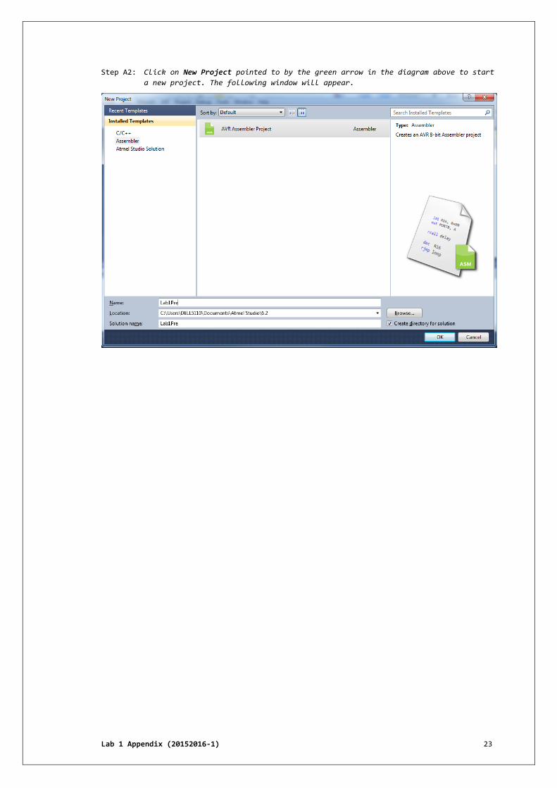
Step A2: Click on New Project pointed to by the green arrow in the diagram above to start
a new project. The following window will appear.

Lab 1 Appendix (20152016-1) 24
Step A3: To create a new assembly project select C from the panel to the left pointed to
by the green arrow. Also type the file Name and Location pointed to by the green
arrows at the bottom of the window. The following window will then appear. I n
this example the projeck name is “Lab1Pre”.

Lab 1 Appendix (20152016-1) 25
Step A4: The window above is the device selection screen for Atmel Studio 6. Scroll down
and select the microcontroller you will be using. The following window will then
appear.
This is the Atmel Studio 6 editor where you type your assembly program. The editor starts
your assembly program for you by providing you with the structure (in comment field) shown
in the editor of the figure above. You may optionally delete (or edit) the structure.
Step A5: Write the program given in Figure A.17(A5), on the Atmel Studio 6 editor.
Explanations on the program are given in the comments fields). Please do not cut
and paste. Its is objectively targetted that by reading then writing back the
program line by line (and referring to A.6 thru A.15, the writer will develope:
1) The experience on typing a program.
2) The good practice to organize code.
3) The knowledge on the assembler directive used and their argument(s).
4) The knowledge on how assembler directive declare locations for writing program
and data in Program memory of the ATmega32 architecture.
5) The knowledge on how assembler directive declare locations for locations for
variable in Data memory of the ATmega32 architecture.
6) The knowledge on how the instructions and their operand(s) are written.
7) The knowledge on function of addressing modes for each instruction: where data
is taken (source) and where data is stored (destination).
Do not copy the comments as-is given in Figure A.17(A5). You are required to
develop your own original comments which can be done as you progressively type out
and understand the sequence of instructions.
/* * Lab1Pre.asm * * Created: 9/8/2015 8:28:38 PM * Author: DELL5110 */ /* Note that hexadecimal number can represented with either the prefix "0x" or "$" It is a good practice to just use either "0x" or "$" but in this lab both is used for demonstration purpose. Note also how comments is declared

Lab 1 Appendix (20152016-1) 26
*/ /* The ATmega32A is a functionally identical, drop-in replacement for the ATmega32. All devices are subject to the same qualification process and same set of production tests, but as the manufacturing process is not the same. Some electrical characteristics differ. In this lab ATmega32 device will be used. */ .include "m32Adef.inc" //Register/Bit Definitions for the ATmega32A /* By including this file "m32Adef.inc" in the assembly program file, all I/O register names and I/O register bit names appearing in the data book can be used. In addition, the six registers forming the three data pointers X, Y and Z have been assigned names XL - ZH. Highest RAM address for Internal SRAM (RAMEND) is also defined ($085F). */ .equ ten = 10 .cseg //Declare Program (Flash) Memory Space .org 0x0 reset: jmp start //RESET vector at address 0x0000 /* When RESET event is invoked, PC <-- 0000. The CPU will execute instruction at pointed by PC. In normal procedure we will force PC to be set to the location of the bootup codes by using the "jmp start" instruction which effectively causes to jump to the address 0x2A. 0x2A is the address in Program memory just after the interrupt vector table of the ATmega32. We can omit this "jmp main" (and straight away continue with the bootup codes) if we are not going to use any interrupt in the program (which are unlikely in normal application of a CPU or microcontroller). */ //Address 0x0002 to 0x002f is reserved for Interrupt vector table .org 0xA /*In this lab1 since we are not going to use interrupt, we are using the vector table area for our program starting at address 0xA*/ start: /* Boot up codes starts here where STACK, I/O control registers and any other global variables used in the operation of the CPU, is initiallised. */ /* Process No: 1. Initialise stack ponter at highest (end) of Data Memory (SRAM). Effectively, SP <-- 0x85F (value of RAMEND which is defined in "m32A.inc") */ ldi R16,low(RAMEND) //r16 <-- (using Immediate addressing mode) out SPL,R16 //SPH <-- R16 (using I/O addressing mode) /*R16 (one of the upper GPRs) is used as the intermediate variable to hold low byte of value RAMEND before being stored to SPL*/ ldi r16,high(RAMEND)//R16 <-- high byte of value RAMEND out SPH,R16 //SPH <-- R16 /*Finally SP<--RAMEND after sequential executions of the four instructions*/ /* Process No: 2. Now we are going to initialise num1 with value $2F*/ ldi r17,$2a //r17 <-- $2a using Immediate addressing mode sts num1,r17 //num1 <--r17 using direct addressing modes /*R17 (one of the upper GPRs) is used as the intermediate variable to hold value $2a before being stored to num1 (absolute address is $60) Finally num1<-- $2a after sequential executions of the two instructions*/ /* Process No: 3. Now we are going to copy data in num1 into temp1*/ lds r17,num1 //r18 <-- num1 using Direct addressing mode sts temp1,r17 //num1 <--r18 using direct addressing modes /*R18 (one of the upper GPRs) is used as the intermediate variable to hold value from num1 before being stored to temp1 (absolute address is $120)' Finally temp1 <-- num1 after sequential executions of the

Lab 1 Appendix (20152016-1) 27
two instructions */ /* Process No: 4. Now we are going to do the calculation of sum = num1 + temp1 + 5 */ lds r0,num1 ;r0 <-- num1 lds r1,temp1 ;r1 <-- temp1 add r0,r1 ;r0 <-- r0 + r1 ldi r16,5 ;r16 <-- 5 add r0,r16 ;r0 < r0 + r1 sts sum,r0 ;sum <-- r0 ;Effectively sum <-- num1 + temp1 + 5 ($59) /* Process No: 5. Now we are going to initialise pointer Register Y with address of numbers3*/ ldi YL,low(numbers3) //YL <-- low byte of address of numbers3 ldi YH,high(numbers3) //YH <-- high byte of address of numbers3 //effectively Y <-- address of numbers3 /* Process No: 6. Now we are going to store value $53 at address pointed by X (value in X)*/ ldi r16,$53 //r16 <-- $53 using R16 as intermediate (one of valid GPR) st Y,r16 //(Y) <-- R16 Using Register Indirect addressing mode /* Process No: 7. Now we are going to store value $35 at address which is 16 byte after (displaced +vely) address of numbers3*/ ldi r16,$35 //r16 <-- $35 using R16 as intermediate (one of valid GPR) std Y+3,r16 //(Y+3) <-- R16 Using Register Indirect with displacement //addressing mode /* Process No: 8. Now we are going to initialise value: $10, $11, $12, $13 and $14 in sequence in the array pointed by numbers3 (i.e address $80, $81, $82, $83 and $84) consecutively by using address register indirect with post increment method X register must be initialise to point to the first address of array numbers3 Consecutively using Register Indirect with post increment mode and r20 is pre-updated (initially r20<--$10 but subsequently r20 incremented) the operation: (X) <-- r20, X <-- X + 1 is executed 4 times */ /*we will need to initialise pointer Register X with address of numbers3*/ ldi XL,low(numbers3) //XL <-- low byte of address of numbers3 ldi XH,high(numbers3) //XH <-- high byte of address of numbers3 //effectively X <-- address of numbers3 /*Now in four consecutively phase: with r20 pre-updated, X <-- r20, x<--x+1 (initially r20<--$10, subsequently r20 incremented)*/ ldi r20,ten //r20 <-- $10: (r20 initialised value $10) st X+,r20 //(X) <-- r20, X <-- X + 1: (effectively [$080] <-- $10, X <-- $081) inc r20 //r20 <-- r20 +1: (effectively r20 <-- $11) st X+,r20 //(X) <-- r20, X <-- X + 1: (effectively [$081] <-- $11, X <-- $082) inc r20 //r20 <-- r20 +1: (effectively r20 <-- $12) st X+,r20 //(X) <-- r20, X <-- X + 1: (effectively [$082] <-- $12, X <-- $083) inc r20 //r20 <-- r20 +1: (effectively r20 <-- $13) st X+,r20 //(X) <-- r20, X <-- X + 1: (effectively [$083] <-- $13, X <-- $084) inc r20 //r20 <-- r20 +1: (effectively r20 <-- $14) st X+,r20 //(X) <-- r20, X <-- X + 1: (effectively [$084] <-- $14, X <-- $085) /* Process No: 9. Now we are going to copy in sequentialy, the string of 1 byte data in address numbers2+0 ($80), numbers2+1 ($81),numbers2+2 ($82) and numbers2+3 ($83) to array pointed by numbers3+3 in REVERSE ORDER (address $67, $66, $65, $64) Effectively sequentially, the following will happen: (numbers3+3) <-- ($numbers2) (numbers3+2) <-- ($numbers2+1) (numbers3+1) <-- ($numbers2+2) (numbers3) <-- ($numbers2+3) */ /*Initially we are going to initialise pointer Register X with address of numbers2 */ ldi XL,low(numbers2+4) //XL <-- low byte of address of numbers2 + 4 ($68)

Lab 1 Appendix (20152016-1) 28
ldi XH,high(numbers2+4) //XH <-- high byte of address of numbers2 + 4 ($00) //effectively X <-- address of numbers2 + 4 ($0068) /*Then we are going to initialise pointer Register Y with $54 (end address of source array)*/ ldi YL,low(numbers3) //YL <-- low byte of $00 ldi YH,high(numbers3) //YH <-- high byte of $01 //effectively Y <-- $050 ld r16,Y+ //R16 <-- (Y), Y<--Y+1: Effectively (r16 <-- ($80), Y<--$81 st -X,r16 //X <-- X-1, X <-- R16: Effectively (X<-- 67, ($67)<-- R16 //Overall effectively: ($67) <-- ($80), Y <--$81 X <-- $66 ld r16,Y+ //R16 <-- (Y), Y<--Y+1: Effectively (r16 <-- ($81), Y<--$82 st -X,r16 //X <-- X-1, X <-- R16: Effectively (X<-- 66, ($66)<-- R16 //Overall effectively: ($66) <-- ($81), Y <--$82 X <-- $65 ld r16,Y+ //R16 <-- (Y), Y<--Y+1: Effectively (r16 <-- ($82), Y<--$83 st -X,r16 //X <-- X-1, X <-- R16: Effectively (X<-- 65, ($65)<-- R16 //Overall effectively: ($65) <-- ($82), Y <--$83 X <-- $64 ld r16,Y+ //R16 <-- (Y), Y<--Y+1: Effectively (r16 <-- ($83), Y<--$84 st -X,r16 //X <-- X-1, X <-- R16: Effectively (X<-- 64, ($64)<-- R16 //Overall effectively: ($64) <-- ($83), Y <--$84 X <-- $63 /* Process No: 10. Now we are going to read 4 successives byte of data array from numbers1 in Program Memory to array numbers4 in data memory */ ldi ZH,high(numbers1<<1);ZH <-- high byte of absolute byte address of numbers1 ($200) ldi ZL,low(numbers1<<1) ;ZL <-- low byte of absolute byte address of numbers1 ldi YH,high(numbers4) ;YH <-- high byte of absolute byte address of numbers4 ldi YL,low(numbers4) ;YL <-- low byte of absolute byte address of numbers4 ldi r17,4 ;Set repeat loop = 4 repeat: lpm r18,Z+ ;R18 <-- (Z),Z <-- Z+1 st Y+,r18 ;Y <-- R18, Y <-- Y+1 dec r17 ;R17 <-- R17-1 brne repeat ;Repeat until (R17==0) /* Process No: 11. Program does an infinite loop (halt at location "here") as it continuously executes "rjmp here" */ here: rjmp here .org $50 //Address to start at 0x100 in Program Memory SS_table: .db $3f,$06,$5b,$4f,$66,$6d,$7d, $03, $7f, $6f //SS_table declared at address $100 numbers1: .db 0x10, 0x1,0x12,0x3,0x14,0x15,0x6,0x7,0x18,0x9 //numbers1 declared at address $10A .dseg //Data Memory(Flash) Space (by default at address start $60) num1: .byte 1 ;num1 declared as 1 byte storage by default at address $60 num2: .byte 1 ;num2 declared as 1 byte storage at next address=0x61 data1: .byte 1 ;data1 declared as 1 byte storage at next address=0x62 data2: .byte 1 ;data2 declared as 1 byte storage at next address=0x63 numbers2: ; .byte 7 ;numbers2 declared at address $64 as a 7 byte array storage endofnumbers2: .byte 1 .org 0x80 //Address to start at 0x100 numbers3: .byte 6 ;numbers2 declared as a 6 byte array storage numbers4: .byte $10 ;numbers2 declared as a 16 byte array storage at address 0x110 temp1: .byte 1 ;temp1 will be declared at address 0x96 temp2: .byte 1 ;temp1 will be declared at address 0x97 sum: .byte 1 ;temp1 will be declared at address 0x98

Lab 1 Appendix (20152016-1) 29
Figure A.17(A5)
Step A6: Closing/Opening an Existing Project.
Whenever it need be, you can always edit existing project that has been created and closed
and close. How to do this can be self-learned.
Debugging A.18.
Debugging is a process of finding logical errors in a program. However though you can use
this process to achieve the objective stated in Step A5.
There are no fixed steps on debugging a program. The concept is that we need to know where
and what caused the bug so that we can do the correct rectification on the program.
Conceptually, to find the bug, we need to know what the input to the program is, and/or
what the output is, and/or whether logically (in decision instruction) it is doing as what
it should be. So to do this we may use one of the following methods:
1. Single Step by Step, using Step Over or Step Into operation.
2. Set breakpoint(s) at location where we want to inspect the input or output of
the program. Then we run (or simulate) until the program reach the breakpoint.
3. Step Over an instruction or function (or procedure) and inspect the input or
output of the program’s instruction or function (or procedure).
4. Step Into the function (or procedure) and inspect the input or output of the
program’s function (or procedure).
5. Note: Step Over an instruction is the same operation as Step Into the
instruction.
Step A7: Selecting Target of Program when to Debug
Atmel Studio 6 allows the target to be selected. If no external target is connected, by
default AVR simulator will be selected. To make/confirm selection select ProjectLab1Pre
Properties.... You can click “Selected debugger/programmer” select available target.

Lab 1 Appendix (20152016-1) 30
a. Starting and Ending a Debug Session in Atmel Studio 6
To start a debug session and halt press Alt+F5 or choose Debug→Start Debugging and
Break from the menu, alternatively, press the toolbar button as illustrated below:

Lab 1 Appendix (20152016-1) 31
To Continuer a debug session (when in Break) and keep executing press F5 or press the
toolbar button with the continue symbol or choose Debug→Continue from the menu as
illustrated below:
To end the debug session use the Stop Debugging button or keyboard shortcut Shift+F5.
b. What is a Break.
The Break is a situation in debug session when execution of instruction is halted. PC
(Program Counter) will hold (pointing) to the next instruction the CPU will execute.
c. Debug control
Several commands are available for controlling the debugger. They are available from
both the Debug menu and several toolbars. The Atmel Studio Integrated Development
Environment (IDE) has two major operating modes: design mode and debug mode. Design
mode is when you are editing the source code project, while debug mode is when you
debug your project. The IDE adapts to modes, and menus an toolbars changes.
Note
Some debug commands are available in design mode, some in debug mode.
In design mode, the available debug commands are those that will start the debug
session, e.g. Start Debugging and Break, Start Debugging, Start without Debugging.
In debug mode, you will find commands like Break All, Step Out and Reset.
Figure A.18(c) shows the pull down menu of the debugging command when the Debug menu
is selected while in Debug Mode:
Figure A.18(c)

Lab 1 Appendix (20152016-1) 32
The following are explanation on some of the commands.
Start Debugging and Break
Starts the debugger, and breaks the execution on the first statement of the program (RESET vector).
Start Debugging
Starts the debugger, and runs the program. In debug mode and stopped, it resumes execution.
Start Without Debugging
Programs the project without starting debugging. For details, see Debug: Start without debugging.
Break All
Halts (breaks) the debugger. Normally we select this when we want to break a running program.
Stop Debugging
Stops and terminates the debug session, and returns to design mode.
Restart
Restarts the debugger and reloads the program.
Reset
Resets the program to the first statement
Step Into
Executes one instruction. When in disassembly level, one assembly level instruction is executed, otherwise one source level instruction is executed.
Step Over
Similar to Step Into, Step Over executes one instruction. However, if the instruction contains a function call/subroutine call, the function/subroutine is executed as well. If a user breakpoint is encountered during Step Over, execution is halted.
Step Out
Continue execution until the current function has completed. If a user breakpoint is encountered during Step Over, execution is halted. If a Step Out command is issued when the program is on the top level, the program will continue executing until it reaches a breakpoint or it is stopped by the user.
Quick Watch and Watches
Adds a Quick Watch for the variable or expression under the cursor.
Toggle Breakpoint
Toggle the breakpoint status for the instruction where the cursor is placed. Note that this function is only available when the source window or disassembly window is the active view.
New Breakpoint
Create a new breakpoint at the location of the cursor.
A breakpoint tells the debugger to temporarily suspend execution of a program when a specific condition takes place, e.g. when a certain instruction is about to be executed.
Breakpoints provide a powerful tool that enables you to suspend execution where and when you need to. Rather than stepping through your code line by line or instruction by instruction, you can allow

Lab 1 Appendix (20152016-1) 33
your program to run until it hits a breakpoint, and then start to debug. This speeds up the debugging process.
Disable All Breakpoints
This function clears all set program breakpoints, including breakpoints which have been disabled.
d. Breakpoint glyphs (icon)
The source windows and the Disassembly window show breakpoint locations by displaying
symbols called glyphs in the left margin. The following table describes these glyphs.
If you rest the mouse on a breakpoint glyph, a breakpoint tip appears with more
information. This information is especially useful for error and warning breakpoints.
Icon Description
Normal breakpoint. The solid glyph indicates that the breakpoint is enabled. The hollow glyph indicates that it is disabled.
Advanced breakpoint. Active/disabled. The + sign indicates that the breakpoint has at least one advanced feature (such as condition, hit count, or filter) attached to it.
Breakpoint error. The X indicates that the breakpoint could not be set because of an error condition.
Breakpoint warning. The exclamation mark indicates that a breakpoint could not be set because of a temporary condition. Usually, this means that the code at the breakpoint or tracepoint location has not been loaded. It can also be seen if you attach to a process and the symbols for that process are not loaded. When the code or symbols are loaded, the breakpoint will be enabled and the glyph will change.
e. Applying Debugging as a learning aid tool.
By using debugging technique you can:
1. Visualise the architecture of the ATmega32A by using Processor View, Memory Views
and I/O Views to identify the physical components in the processor.
2. You can note the relationship between each view. For instance the data in R27:R26
represent the data in X pointer register (refer Figure A.5 (d)). Try changing R26:R25 and you will find that X will also change.
3. By single stepping (Step Over or Step Into) an instruction you can find out or
confirm your understanding on the execution of the program i.e. the changes of
Registers or Memory Location as defined in the Instruction Set Reference, the
location of data taken from or send to as defined by the addressing modes of the
instruction.
4. By Stepping Into a subroutine call (CALL or RCALL instruction), you can find out
or confirm your understanding on the execution of the Instruction, i.e. the
changes of PC and STACK and trace (single step) into the subroutine.
5. By Stepping Over a subroutine call (CALL or RCALL instruction), you can find out
or confirm that your understanding on the execution of the whole subroutine
without getting into the subroutine.
6. You can simulate condition before you execute an instruction by setting contents
the register or memory location that is used by the instruction before executing
it so that you can visualise/confirm the effect of the register or memory location
data in towards the execution of the instruction.
7. By tracing through a program you can confirm/examine the program flow of a program
and you can visualise/confirm that PC (Program Counter) directs the flow of the

Lab 1 Appendix (20152016-1) 34
program. So you can see how Program Flow Instructions (Branch Instructions)
changes the PC in accordance to the Instruction Set reference.
8. You can use Breakpoints to force the program to stop at the any of the Breakpoints
the program will pass through.
9. By using Breakpoints you can execute your program such that it skip a sequence of
code that you do not want to trace and stop at the instruction that you want to
begin you single stepping. This will help you overcome repeating tracing that code
that you have confirmed not needed (to save time and energy doing the tedious
stepping over) especially after you restart the program to test the working of the
program after making changes on code.
Note: Select Debug Stop Debugging to clear all registers and Memory contents to
avoid confusion of old data contents during previous debugging process.
10. Certain instruction can only be executed in the program is running so you cannot
use single step method. By setting breakpoints at the instruction you can stop the
program when the certain event occurs. From that breakpoint you can trace the
program if needed. These event can occur from interrupts INT0, INT1 , INT2, ADC or
Timers or input from switches that is check by conditional branch instructions.
11. When you are debugging a program that reads data from Digital I/O ports, you can
simulate the input by setting the revenant PINxn bit before you trace or run the
program. By doing this you can check the flow of the program that check the status
of the input.

Lab 1 Appendix (20152016-1) 35
Viewing the Disassembly of the ATmega32 Program A.19.
Step A8: To view the disassembly Display, in Debug mode Select
DebugWindowsDisassembler which will open Disassembler window Tab as shown in
Figure A.19(A7). The Disassembly window is only available when debugging.
The disassembly window shows your program code disassembled. Program execution and AVR
instructions can be followed in this view. By right clicking inside the Disassembly window
you will be able to set breakpoints, run to the position of the cursor or go to the source
code. You cannot modify the source code from the Disassembly window.
Figure A.19(A8): Disassbler View
In addition to assembly instructions, the Disassembly window can show the following optional information: 1. The next instruction to be execute. Identified in box with circle #1
2. Memory address where each instruction is located. For native applications, this is the actual memory address. Identify labels address from the respective instruction. Identified in box with circle #2
3. Code bytes byte representations of the actual machine. Identified in box with circle #3
4. Source code from which the assembly code derives. Identified in box with circle #4.
5. Symbol names for the memory addresses. Identified in box with circle #5.
6. Original source code instruction. Not Shown in Figure.
3
2
4
4
4
4 3
1

Lab 1 Appendix (20152016-1) 36
Editing values and bits in break mode A.20.
When the project is in debug break mode, any value can be changed by clicking the value
field and writing a new value. Some values and bits cannot be modified as they are read-
only, and some bits may be write-only. See the documentation for each device for more
information. When a bit or value is set, it is immediately read back from the device,
ensuring that the I/O View only displays actual values from the device. If a new value is
set, but the I/O view does not update as expected, the register might be write-only or
simply not accessible.
When a register has changed since last time it was displayed, it will indicate so with a
red coloured value and bits in the display. If a bit has been set since last time, it will
be solid red. If it has been cleared it will simply have a red border. This feature can be
toggled on or off in the toolbar.
Viewing the ATmega32 Processor’s Registers A.21.
Step A9: Select Debug→Windows→Processor View. The processor view offers a simulated or
direct view of the current target device MPU or MCU. In you can see a partial
list of the simulated device's ATxmega32/ATmega32A registers.
Figure A.21(A9): Processor View window

Lab 1 Appendix (20152016-1) 37
The program counter shows the address of the instruction being executed.
The stack pointer shows the application's current stack pointer value.
The X, Y and Z registers are temporary pointers that can be used in indirect passing or
retrieving arguments or objects to and from functions. Cycle counter counts the cycles elapsed from the simulation’s start.
Status register or SREG shows the currently set flags.
Further on you will be able to toggle a setting for displaying the flag names.
The stop watch field allows you to make rudimentary profiling of your application. It is influenced
by the frequency set in Frequency field, which defines target MCU/MPU frequency, in case when
the prototyping board is connected.
Each register can be displayed in hexadecimal, decimal, octal and binary (flag) format by right-
clicking and choosing Display in binary, etc., or Display in... . Each field can also be modified, as
shown in the below image. If a field is a status or flags register, composed of a number of the
one-bit flags, you can toggle individual flags by clicking on them -
The processor view is only active in the debug mode.
Viewing the ATmega32 Memory Space A.22.
The memory view gives you an outline of the memory.
It is possible to select among the attached memories to see all the segments by switching
between them in a Segment drop-down menu on top of the memory view, you can also specify
the starting address for the memory view window in the Address form field on top of the
memory view.
In order to specify the address you can use either a normal hexadecimal entry or an
expression: See the section called “Expression formatting”. The Columns drop-down menu allows
to specify how many byte-aligned memory columns you wish to see at one time, most often
that should be left at Auto setting, but if you have to manually check a fixed-length type
values and you know how many words or bytes those values occupy, you could align the
memory view so that each row will correspond to a desired number of values.
a. Viewing Instruction data in Program Memory
Step A10: Select Debug WindowsMemory viewWindow 1, or Ctrl+Alt+M+n where n is the
memory's number (1).
Figure A.22 (a): Memory 1 window with “prog Flash” (Program memory), address start at 0x00
and Auto column selected.

Lab 1 Appendix (20152016-1) 38
This is the machine code which is also displayed in a different format shown in
display in Figure A.19(A7-1). Inspect address 0x0000 and 0x000A the similarity and
difference between the two displays.
b. Viewing .DB data in Program Memory
Step A11: Now change the setting such that address = 0x0050 * 2 = 0x00A0 (Refer Section
A.3 Figure A.3). This is the Address of SS_table declared in program memory of
program “Lab1pre”.
Also set Columns : 2. The display will be in Figure A.19(A7-2).
Figure A.22(b): Location and contents of SS_table declared in Program Memory of
program “Lab1pre” using “.DB” assembler directive.
You will see the physical address of the “.DB” assembler directive in Program
Memory and the content of the memory locations from the .DB declarations.
Using Watch window to determine address of label (address may be used as A.23. variables)
Step A12: Select Debug WindowsWatch.
Figure A.23(A12): Example of Watch window for some of the variable from Lab1Pre project.
1. The identifier under the “Name” are valid labels declared in the program being
debug that have to be entered manually.
2. Watch window can be used to determine value of labels declared in the program
3. Using this value as address in memory window, you can watch content of the label
(as variable) by watching the address.
Debugging the program Using Single Step A.24.
In Debug mode There are two commands to single step through the code. These are "Step
Over" <F10> and "Step Into" <F11>. The difference between these commands is
that <F10> does not trace into subroutines. Since our example does not contain any
subroutines, there is no difference between these commands in this example.

Lab 1 Appendix (20152016-1) 39
Step A13: Close “Lab1Pre” and reopen the project. You should be able to find the folder,
otherwise search for “Lab3pre.atsln. You should see the following display. If
there is no “Lab1Pre.asm” double-click the “Lab1Pre.asm” icon in the “Solution
Explorer” window.

Lab 1 Appendix (20152016-1) 40
Step A14: Make sure that the “Selected debugger/programmer” is on “Simulator”.
Step A15: Select “Start Debugging and Break” command and you will see the following
display. If the “Processor” window is not open, open it (Debug
Windowprocessor View)
Figure A24(A15): Debug and Processor View on ““Start Debugging and Break” command.
The yellow arrow will be pointing to the instruction “jmp start” addressed (pointed) by
Program Counter which is at 0x000000 which is the next instruction to be executed.

Lab 1 Appendix (20152016-1) 41
Single Step through your program A.25.
Step A16: Noting that PC is at address “0x00000A”, To Single Step over instruction “jmp
start” strike the [F10] key once):
Note that the word in red indicates the register that is affected from the
execution changes from the previous value. If the field is affected from the
execution but the result is the same value as before (no change), the colour of
the word in the fields will be black (as if the register is not affected from
the instruction – so be careful not to assume so).
This command will cause the simulation to execute the instruction “jmp start”
pointed by Program Counter and stop at the next instruction which in this case
will be “ldi R16,low(RAMEND)” at address 0x000A shown by the yellow arrow. The
Program Counter will be updated to point at the next instruction which is 0x000A
which is also the address of “start”.
Figure A25(A16-1): Display after single-stepping instruction at address 0x000000
(execution of “jmp start”)
Referring to the instruction “JMP” in page 82 the in the file “AVR-Instruction-Set
2002.pdf” as shown below, the PC take the value of the operand that is “start” and the is
no changes in the SREG.
To check the Status Register, you will need to view the Processor window. Grey colour text in
the boxed (eg. C for Carry bit) represent that that the bit is 0. A black font colour
represents that that the bit is 1 (not shown right now).

Lab 1 Appendix (20152016-1) 42
Figure A25(A16-2): JMP instruction ” in page 82 the in the file “AVR-Instruction-Set 2002.pdf”

Lab 1 Appendix (20152016-1) 43
Step A17: Single step again over instruction “ldi R16,low(RAMEND)” and inspect content of
R16 and SREG (Status Register).
This command will cause the simulation to execute the instruction “ldi R16,low(RAMEND)” and stop at the next instruction which in this case will be “out SPL,R16” at address 0x000B shown by the yellow arrow. The Program Counter will be updated to point at the next instruction which is 0x000B. R16 will be loaded with 0x5F. Red color on the word denotes that the value has changed
Figure A25(A17): Display after single-stepping instruction at address 0x00000A (execution
of “ldi R16,low(RAMEND”) “out SPL,R16”.

Lab 1 Appendix (20152016-1) 44
Step A18: Single step again and inspect content of R16 and SREG (Status Register).
This command will cause the simulation to execute the instruction “out SPL,R16”
pointed by Program Counter and stop at the next instruction which in this case
will be “ldi R16,high(RAMEND)” at address 0x000C shown by the yellow arrow. The
Program Counter will be updated to point at the next instruction which is 0x000C
which is also the address of “ldi R16,high(RAMEND)”.
Do the single stepping until the instruction “rjmp here”.
If you want to check the memory location, you may check using the memory window (refer
Section A.22).
Using Breakpoint A.26.
Breakpoints are a method of halting execution flow. By adding a breakpoint in the assembly
code we can run the program at full speed, and it will be stopped at the line with the
breakpoint. By now you have noticed that you have to press<F11> three times to go through
the loop once. We will add a breakpoint at the by placing the cursor on the instruction in
the source view window and press <F9> (or the "Toggle Breakpoint" in the "Debug" menu ). A
red circle will appear in the left margin of the source view window as shown. By
pressing <F5> or "Run" from the "Debug" menu the program will start running and break
(stop) at the instruction with the breakpoint.
There may be situations where we have single stepped through far in the program but you
may need to reverse a few steps back to review a result. We will need to Stop Debugging
and start over sequential single stepping again until we reach the instruction we want to
review which can be unnecessarily tedious.
The best method to overcome this is to set a breakpoint at the instruction we want to
stop, RUN the program so that it will stop at the breakpoint it meets. Then you may single
step through from there.
To set a breakpoint, click on any row to put the cursor on the line of the instruction
where you want to break (stop) as show below (in this example “ldi r20,ten” ). Do not
select the whole line. Then press F9.

Lab 1 Appendix (20152016-1) 45
You will see a red dot on the side of the instruction as shown in the following display.
You may set another (or many) breakpoint(s) that we need so that we may CONTINUE running
the program until it meets the next breakpoint.
You may remove any breakpoint by pressing F9 or clicking the Toggle Breakpoint icon. To
remove all breakpoint, select Debug|Remove all Breakpoints or click the Remove all
Breakpoints icon.
Stopping Debug A.27.
Step A19: Stop Debugging by selecting the menu Debug| Stop Debugging.
Calculating Execution Time A.28.
a. Calculating Execution Time for Sequential Code
To determine the execution time (ET) for a piece of AVR assembly code you will need
the following information:
The clock frequency of the AVR microcontroller the code is running on.
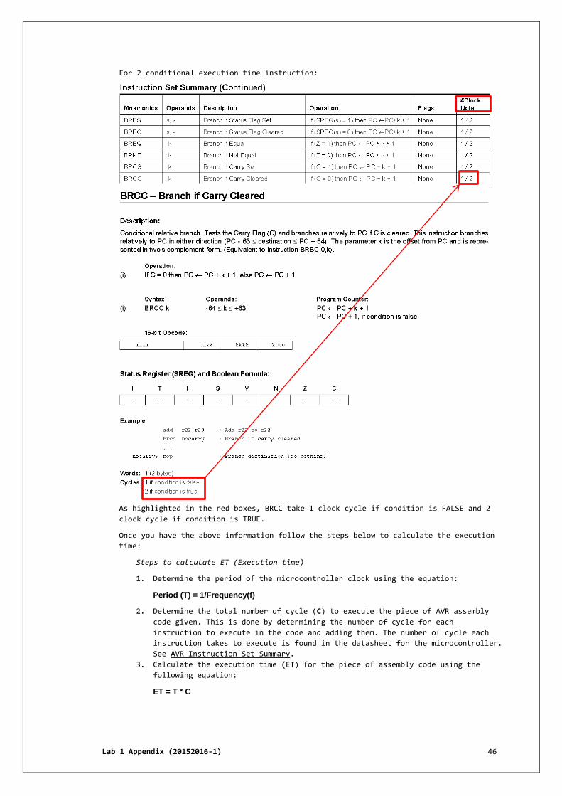
The information sheet that tells the number of cycle each instruction requires to execute.
Refer to “Instruction Set Summary.pdf” under the “#Clock Note” column or “AVR-
Instruction-Set.pdf” on the “Cycles” title. Respective example are shown below:
In snippet of “Instruction Set Summary.pdf” shown below:
For single execution time instruction
As highlighted in the red boxes, LDI takes 1 clock cycle to execute
Lab 1 Appendix (20152016-1) 46
For 2 conditional execution time instruction:
As highlighted in the red boxes, BRCC take 1 clock cycle if condition is FALSE and 2
clock cycle if condition is TRUE.
Once you have the above information follow the steps below to calculate the execution
time:
Steps to calculate ET (Execution time)
1. Determine the period of the microcontroller clock using the equation:
Period (T) = 1/Frequency(f)
2. Determine the total number of cycle (C) to execute the piece of AVR assembly
code given. This is done by determining the number of cycle for each
instruction to execute in the code and adding them. The number of cycle each
instruction takes to execute is found in the datasheet for the microcontroller.
See AVR Instruction Set Summary.
3. Calculate the execution time (ET) for the piece of assembly code using the
following equation:
ET = T * C

Lab 1 Appendix (20152016-1) 47
Example 1
Calculate the execution time for the following piece of assembly code given that
the code will be running on an Atmel AVR 8-bit micro-controller being clocked by a
4MHz oscillator.
LDI R16, 0xFF
LDI R17, 0xEE
ADD R17, R16
MOV R20, R17
Solution
Step 1 - Determine the Period (T)
T = 1/f = 1/4*106 = 0.250µs
Step 2 - Determine Total Number of Cycles for execution (C)
; Instruction # cycles to execute
LDI R16, 0xFF ; 1
LDI R17, 0xEE ; 1
ADD R17, R16 ; 1
MOV R20, R17 ; 1
; _______________________________________________________
; Total # of cycles for execution (C) = 4
Step 3 - Calculate Execution Time (ET) using information from steps 1 & 2
ET = C * T = 4 * 0.250 = 1µs

Lab 1 Appendix (20152016-1) 48
b. Calculating Execution Time for Code with Single Loop
Example 2
Calculate the execution time for the following piece of AVR assembly code given
that the code will be running on an Atmel AVR 8-bit micro-controller being clocked
by a 1 MHz oscillator.
LDI R16, 5
Again: DEC R16
NOP
BRNE Again
NOP
NOP
Solution
Step 1 - Determine the Period (T)
T = 1/f = 1/106 = 1 µs
Step 2 - Determine Total Number of Cycles for execution (C)
; Instruction # cycles to execute
LDI R16, 5 ; 1
Again: DEC R16 ;-----|
NOP ; | A
BRNE Again ;-----|
NOP ; 1
NOP ; 1
;
_______________________________________________________
; Total # of cycles for execution (C) = 3 + A
The total number of cycles for the execution of the code is given as (3 + A). In calculating the total number of cycles for execution, in this case, it must be
taken into consideration that the block of code labeled A is executed more than
once because it forms a loop.
What is done here is that we look at the block of code which construct the loop as
a single instruction for which we will determine the number of cycle for execution
next.
Calculating the number of cycles for block A
; Instruction # cycles to execute
Again: DEC R16 ;-----| 1
NOP ; | 1
BRNE Again ;-----| 2
; _______________________________________________________
; Total # of cycles for execution of A = 5*(1+1+2) - 1
In this code the loop is controlled by the value in R16 which is 5. So the code in
block A is done 5 times. This result in C = 3 + A = 3 + [5(1+1+2) -1] = 22cycles.
One important point to note here is that the BRNE instruction takes 2 cycle to
execute when it is true and 1 cycle when the condition is false. So for the 5
times the BRNE instruction is executed 1 time the condition is false which is why
we subtract 1.
Step 3 - Calculate Execution Time (ET) using information from steps 1 & 2
ET = C * T = 22 * 1 = 22 µs

Lab 1 Appendix (20152016-1) 49
c. Verifying the Calculated Execution Time
Step 1: Open AtmelStudio and create a new AVR assembly project.
The entire code in the Atmel Studio editor should be similar to that below:
/* * DelaywithLoop.asm * * Created: 1/8/2015 11:33:08 PM * Author: DELL5110 */ .org 0 reset: jmp boot .org 0x2a boot: ; Instruction # cycles to execute LDI R16, 5 ; 1 Again: DEC R16 ;-----|2 NOP ; |1 A = 5*(1+1+2)-1 = 22 BRNE Again ;-----|1 NOP ; 1 NOP ; 1 ; _______________________________________________________ ; Total # of cycles for execution (C) = 3 + A shell: RJMP shell
Step 1: Go to the “Debug” menu in the Atmel Studio and select “Start Debugging and
Break”. You should get a screen looking like the one below:

Lab 1 Appendix (20152016-1) 50
Atmel Studio is now in simulation mode notice the yellow arrow, which indicates
the microcontroller is about to execute this line of code.
Also notice the 'Processor' window pane to the left, which indicates the value of
the Cycle Counter, Frequency, Stop Watch, etc. At this point the Cycle Counter and
Stop Watch is at 0, indicating that no instruction as been executed. The Frequency
for this simulation is set to 1 MHz.
Step 2: Single Step to label “boot” and you will get the following display:
Note that Cycle Counter = 3 and Stopwatch = 3.
Step 3: Position the cursor at the beginning of the line “shell: RJMP shell”. Then
go to the Debug menu and select Run to Cursor.
The simulator will now execute all the instruction up to where the cursor
is located. You should now see an update 'Processor' window pane showing the number of cycles that has passed to execute up to this point in the code, given by Cycle Counter.
We are interested in the Stop Watch value which gives the time taken to execute the instructions up to this point in the code which is 25 cycles or
25 µSec. That is the Execution Time for from instruction at “boot” to instruction at “shell” = 25-3 = 22 cycle or 22 µSec. This is equal to what
we have calculated previously.

Lab 1 Appendix (20152016-1) 51

Lab 1 Appendix (20152016-1) 52


![[ASM] Lab1](https://static.fdocuments.net/doc/165x107/588121881a28abb9388b706b/asm-lab1.jpg)