
Embedded Design with The Xilinx Embedded Developer Kit Xilinx Training.

EECS150 Spring 2013 Lab 5
1
Lab 5B: Xilinx Embedded System
Development
University of California, Berkeley
Department of Electrical Engineering and Computer Sciences
EECS150 Components and Design Techniques for Digital Systems
John Wawrzynek, Shaoyi Cheng, Vincent Lee
Due March 6th, 2013 @ 2:00PM
Table of Contents
0 Introduction ........................................................................................................................................................................................................1
Partners ..............................................................................................................................................................................................................1
1 PreLab ..................................................................................................................................................................................................................2
2 Lab Procedure..................................................................................................................................................................................................2
Xilinx Embedded Development Kit (EDK) and MicroBlaze ..................................................................................................2
Hardware System .........................................................................................................................................................................................2
Software Design ............................................................................................................................................................................................6
Adding Coprocessor ................................................................................................................................................................................ 10
Implementing GCD Coprocessor with ISE.................................................................................................................................. 12
Using Coprocessor in Software ......................................................................................................................................................... 15
Checkoff .......................................................................................................................................................................................................... 15
0 Introduction
In this lab you will implement a simple processor based system using Xilinx Embedded System
Development Kit. Instead using Verilog, you are going to select components from a library of IPs and
connect them in the Xilinx GUI. In addition, using the Xilinx SDK, you will create a short program to run on
the processor, communicating with the host workstation using serial connection. Finally, you will integrate
a new hardware module into the existing system, and control it with software running on the processor.
Partners
You are permitted to work with a partner for this lab. You will be checking in your system and associated
files to the Git repository, you are required to work with your project partner.

EECS150 Spring 2013 Lab 5
2
1 PreLab
For the prelab, do the following:
1. Get the lab distribution from the class website.
wget http://inst.eecs.berkeley.edu/~cs150/sp13/lab5/lab5B.tar.gz
tar –zxvf lab5B.tar.gz
2. Read http://www.xilinx.com/support/documentation/ip_documentation/fsl_v20.pdf. Make sure you
understand how the FSL protocol works.
2 Lab Procedure
Xilinx Embedded Development Kit (EDK) and MicroBlaze
The embedded systems are complex. In addition to making sure the hardware and the software are both working, the designer also needs to integrate the two components so they can function as one system. To simplify this process, Xilinx offers a set of tools including:
Xilinx Platform Studio (XPS) The XPS is the development environment used for designing the hardware portion of the embedded system. The designer can quickly construct a system from a library of predefined cores. The tool also allows the designer to integrate his/her own IP cores into the system. Software Development Kit (SDK)
The SDK is an eclipse based IDE complementary to the XPS. It is used for C/C++ embedded software application creation and verification.
A Xilinx embedded system is constructed around one or more MicroBlaze processors. The MicroBlaze is a 32 bit RISC-architecture soft-CPU developed by Xilinx for use on their FPGA devices. It can be heavily customized to the needs of the target application by configuring its properties such as instruction and data cache sizes, use of a memory management unit, use of a floating point unit etc. In this lab, we will be using a very simple configuration just to demonstrate the use of the EDK flow. In general, to design an embedded processor system, you need the following:
Hardware components
Memory map
Software applications
The XPS and SDK make it easy for the users to create and modify any of the three aspects of the design.
Hardware System
The system we are going to construct includes the following hardware components:
MicroBlaze
Local Memory Bus (LMB)
o LMB_BRAM_IF_CNTLR
o BRAM_BLOCK
Processor Local Bus (PLB)

EECS150 Spring 2013 Lab 5
3
o XPS_UARTLITE
o MDM
Fast Simplex Link (FSL)
o User defined coprocessor
To use Xilinx Platform Studio, type the following command:
% xps
Select Create New Project Using Base System Builder to open the Create New Project Using BSB
Wizard dialog shown below.
Click the Browse button under New Project and specify a location for the new project file (system.xmp).
Make sure the PLB system is selected under Interconnect Type. To facilitate the creation of systems on
our FPGA board, a board definition file is provided in the lab distribution. To point the tool to this file,
under Set Project Peripheral Repository Search Path, choose the lib directory in the lab distribution
(lab5B/). Press OK to create the new project.
In the next dialog box, choose I would like to create a new design and press Next. This brings up a board
selection dialog. As we have provided the board definition to the tool, you can find XUPV5-LX110
Evaluation Platform in the Board Name drop down menu. Select this board and press Next to bring up the
System Configuration dialog.
As we have mentioned earlier, the XPS creates processor based systems. In this lab, to keep things
simple, we will use a single-processor system, which is the default selection. Press Next to go to
Processor Configuration. Change the System Clock Frequency to 50MHz, this relaxed timing constraint
would give the backend an easier job in place and route, which in turn would shorten the compile time for
the hardware platform. Change the size of local memory to 64KB. Press Next and you should see the
Peripheral Configuration dialog.

EECS150 Spring 2013 Lab 5
4
The MicroBlaze processor can be connected to many different cores. Some of these will be useful when
you are implementing your own project. However, in this lab, we will use a minimal set of peripherals to
showcase the functionality of a simple embedded system. Remove all peripherals except RS232_Uart_1,
dlmb_cntlr and ilmb_cntlr. The RS232_Uart_1 will be used to communicate with the host workstation,
while the dlmb_cntlr and ilmb_cntlr are used by the processor to access the local memory (Block RAM).
Click Next to go to the cache configuration page. As we are not using any off-chip memory for this lab,
there is no caching necessary, click Next to skip this step.
You should now see a summary showing the address mapping of each of the peripherals. These are
automatically generated according to the size of the address range assigned to the peripheral, which can
be modified later. Click Finish to complete the system creation.

EECS150 Spring 2013 Lab 5
5
From the System Assembly View, you can see a MicroBlaze based system with the specified peripherals
has been generated, and all the connections between components are created accordingly. The local
memory bus (LMB) is used by the MicroBlaze core to control the dlmb_cntlr and ilmb_cntlr modules (the
microblaze_0 is the master while the controlled modules are the slaves). Meanwhile, the PLB bus is used
to connect to the RS232_Uart_1 component.
Switch to the Addresses tab to examine the address mapping for each peripheral, Change the size of the
address map and observe how the range of the address is updated automatically. Remember to change
everything back.
On the left hand side of the XPS window, there are several buttons. Run DRCs check the design against
a set of design rules. Under Implement Flow, Generate Netlist implements the design using the Xilinx
backend, going through synthesis and place and route to create the final netlist. Generate BitStream
generates the actual bitstream using bitgen. Export Design is used to create a hardware platform
description, which can be used for software development. Exporting the design will automatically invoke
the generation of netlist and bitstream, so press the Export Design button to bring up the dialog box
shown below. Executing this is equivalent to running make and will take a while (30-40 min) so we
recommend doing something else while you wait.
Click Export & Launch SDK to implement the design and start the software development environment.

EECS150 Spring 2013 Lab 5
6
Software Design
When the Xilinx SDK is launched, you will need to specify a workspace directory. Click OK and soon you
will see a welcome page, close it and you should see the IDE interface shown below.
There are three files used to capture the information of the exported hardware platform. The
system.xml file contains the information about the IP cores used in the design. The system.bit file is
used for programming the FPGA device while the system_bd.bmm file is used by the SDK for loading
memory onto the target board. When we create a software project in Xilinx SDK, we will need to refer to
the hardware platform the compiled program is meant to run on.
In the IDE, select FileNewXilinx C Project, name your project GCD. Under Select Project Template,
choose Empty Application. You will populate this C project with a main function which takes in two input
numbers and compute the greatest common divisor.

EECS150 Spring 2013 Lab 5
7
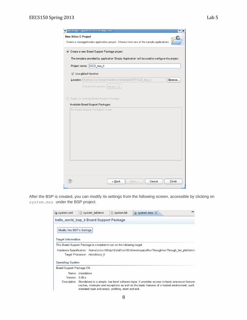
Press Next to bring up the Board Support Package creation screen. The Board Support Package (BSP) is
a collection of libraries and drivers that form the lowest layer of your application software stack. Your
software applications must link against or run on top of a given board support package using the provided
Application Program Interfaces (APIs). In our case, change the project name to GCD_bsp_0 as shown in
the figure below, leave the rest of the default options as they are set and press Finish, the board
supporting package will be automatically created.
EECS150 Spring 2013 Lab 5
8
After the BSP is created, you can modify its settings from the following screen, accessible by clicking on
system.mss under the BSP project.

EECS150 Spring 2013 Lab 5
9
Click the Modify this BSP’s Settings button and you can see an overview of the OS and the hardware
platform we use. In this lab, to keep things simple, we only have a basic software layer (standalone)
instead of a fully functional OS. Click standalone under Overview to bring up the screen below.
As you can see, we will be using the RS232_Uart_1 for both input and output for our program. The serial
port of your workstation has already been connected to the FPGA board using serial cable, through which
the MicroBlaze will be receiving and sending data. In the application running on the processor, the
communication with the host workstation will be performed as read from STDIN and write into STDOUT.
Of course these settings can be modified to suit your need in your own project, if you choose to work with
the EDK flow. Click Cancel to exit the BSP settings screen, and copy the gcd.c file in the lab distribution
(under src/software) into the src directory under GCD project under your workspace directory.
This program will read two numbers from the STDIN and print the greatest common divisor back to
STDOUT. To interact with the MicroBlaze processor running this program, before you program your
FPGA board and load your program, open up a terminal in your workstation and run:1
% screen $SERIALTTY 9600
This tells screen, a highly versatile terminal emulator, to open up the serial device with a baud rate of
9600. Now, go back to the Xilinx SDK, and select Xilinx Tools Program FPGA to bring up the following
dialog:
1 Note that if someone else has locked the serial cable on your workstation, you will not be able to execute this command. Since we don’t have sudo access, the only way to resolve this problem is to either find the offending user and have him kill his session, or reboot the computer.

EECS150 Spring 2013 Lab 5
10
To program the FPGA, use the bitstream and BMM file from the exported hardware platform. For the
software configuration, choose GCD.elf in the GCD project under GCD/Debug. Click Program to
configure the FPGA and load the gcd program.
If your design is working properly, after the FPGA is configured, you should see instructions being printed
to the terminal you opened earlier. The first line you should see is:
GCD program started, please enter two positive numbers.
You can follow the displayed instructions and get the gcd of any two positive numbers. Close the SDK
after you are finished.
To close screen, type Ctrl-a then shift-k and answer y to the confirmation prompt. If you don't close
screen properly, other students won't be able to access the serial port. Use screen -x to re-attach an
improperly closed screen session.
Adding Coprocessor
In many cases, people add coprocessors to take over computationally intensive parts of the program. In
this lab, we will create a coprocessor so the computation of gcd can be offloaded from the MicroBlaze.
The creation and integration of user coprocessors are supported by the Xilinx EDK. Using the XPS and
the SDK, we can modify the existing system to take advantage of the coprocessor we design.
Run the XPS again by running:
% xps
Choose Open Project, and open the system.xmp file you created earlier. From the XPS GUI, select
Hardware Create or Import Peripheral to bring up the wizard, press Next to go to the Peripheral Flow
dialog. As the coprocessor has not been created, select Create templates for a new peripheral. Press
Next and you will be asked where the new peripheral should be stored, use the default and go to the next
page. Name the new peripheral gcd_coprocessor and move on to the Bus Interface selection dialog.

EECS150 Spring 2013 Lab 5
11
Select Fast Simplex Link (FSL), which provides a point to point communication between any two modules
on the FPGA. We will use FSL to couple the gcd coprocessor with the MicroBlaze core. Press Next to
move on to the FSL Bus Interface Settings.
As the FSL is unidirectional, in order for the coprocessor to pass back the computed value, we would
need to have two FSL links. The first will be used by the CPU to send the two input numbers to the
coprocessor while the second will be carrying the result back to the CPU. As the gcd algorithm takes in
two inputs and produces one output, the number of input/output words should be set accordingly. After
you press Next, the Peripheral Implementation Support dialog will allow you to specify the language for
the example peripheral, and if you wish to have the tool generate support infrastructure for the hardware
and software implementation. Check all three boxes and continue.
In the Driver Settings dialog, you can configure the driver API for using the coprocessor. In our case, the
number of input arguments can either be one or two since we have two input words. It should be apparent
to you that when you are using the coprocessor in your program, the input numbers should be placed in
the input array(s) while the result can be read out of the output array. Use one input and one output
argument for the driver API and continue to the summary page. Click Finish to generate the template for
the new peripheral and return to the XPS GUI.
You may notice that under the IP catalog in the XPS, a new category, Project Local PCores is created.
Expand this category and you can see the gcd_coprocessor being listed. However, the coprocessor is not
yet added to our system. Right click on it and choose Add IP, the coprocessor should appear in the
system assembly view, but it is still not connected to any of the existing components. To build up the link

EECS150 Spring 2013 Lab 5
12
between the coprocessor and the MicroBlaze, select HardwareConfigure Coprocessor to bring up the
coprocessor manager. Add gcd_coprocessor to the Connected Coprocessors list and press OK, the
updated system assembly view should be similar to the one shown below:
Implementing GCD Coprocessor with ISE
When the coprocessor template is generated, an ISE project is also created to facilitate the
implementation of the module. In the past few labs, you have been using various components of the ISE
software. In this lab, we will use the ISE GUI for Verilog editing, synthesis and simulation. Start ISE by
running:
% ise
Go to FileOpen Project, navigate to the directory for your XPS project. Under this directory, find
pcores/gcd_coprocessor_v1_00_a/devl/projnav/gcd_coprocessor.xise, this is the ISE
project file. Select it and click Open

EECS150 Spring 2013 Lab 5
13
.
In the Hierarchy view of the project (on the left of the screen), double click the gcd_coprocessor module
to open up the Verilog file in the HDL editor of ISE.
In the earlier part of the lab, you have used the gcd algorithm written in C. Now you are going to
implement the same algorithm using Verilog. An important aspect in implementing the gcd coprocessor is
to understand how to use the FSL interface to get data from the processor and write the result back.
Read over the generated gcd_coprocessor.v to understand how the example module performs read
and write. In this generated example, there are multiple clocks, but only one of them is actually used. Also
there are other control signals which are not driving anything. In your own project, you may be able to
take advantage of a separate clock domain or use the extra control signals to make a more efficient
accelerator.
When you finish editing gcd_coprocessor.v,save it. Some syntax errors can be immediately
detected by the editor, and an error message will be shown in the Console window towards the bottom of
the IDE. More subtle errors can be caught when you synthesize the design, which can be done by
double-clicking Synthesis-XST under Processes (on the left of the IDE). After resolving all syntax
problems, simulate the design to verify its functionality.
We have provided a simple testbench, called Testbench that will run a test on a pair of numbers. To
simulate the design in ISE, select ProjectAdd Source, go to the directory of the lab distribution and
open Testbench.v under src/hardware/sim.
EECS150 Spring 2013 Lab 5
14
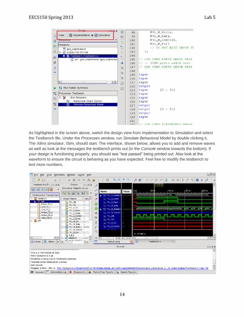
As highlighted in the screen above, switch the design view from Implementation to Simulation and select
the Testbench file. Under the Processes window, run Simulate Behavioral Model by double clicking it,
The Xilinx simulator, ISim, should start. The interface, shown below, allows you to add and remove waves
as well as look at the messages the testbench prints out (in the Console window towards the bottom). If
your design is functioning properly, you should see “test passed” being printed out. Also look at the
waveform to ensure the circuit is behaving as you have expected. Feel free to modify the testbench to
test more numbers.

EECS150 Spring 2013 Lab 5
15
After verifying the functionality of your module, go back to XPS. As the hardware platform has been
changed, select HardwareClean Bitstream, and press Export Design in the Navigator. Choose Export &
Launch SDK. After the hardware compilation, when SDK is launched again, the BSPs in the original
workspace will be automatically updated. Then the coprocessor is ready for use by your software
application.
Using Coprocessor in Software
As the coprocessor has been implemented and integrated into the hardware system, software changes
are needed to make use of it. When the example coprocessor was generated, a skeleton for the driver
was also created. It is located in the driver/src directory under the XPS project. You should find four
files gcd_coprocessor.c, gcd_coprocessor.h, gcd_coprocessor_selftest.c and
Makefile. In gcd_coprocessor.h, a macro has been defined, which writes the input data into the
coprocessor and reads the result out of it. Meanwhile in gcd_coprocessor_selftest.c, the defined
macro is employed to actually use the coprocessor. Make sure you understand these two files. In more
complex peripherals, additional functions can be added to gcd_coprocessor.c to exercise the
coprocessor in different ways. For this lab however, the generated macro is sufficient.
Copy gcd_coprocessor.c and gcd_coprocessor.h from the driver directory to the GCD project
we created earlier in the SDK. Edit the computeGCD function in gcd.c to use the gcd_coprocessor. Feel
free to borrow code from the gcd_coprocessor_selfTest.c. Don’t forget to include the appropriate
header file for the coprocessor.
Note: for the application to work properly, you should define both the input_slot_id and output_slot_id to
be 0. The generated gcd_coprocessor_selfTest.c points them to two compile time constants
which are supposed to be in xparameters.h but are actually absent. In your own project, if you have
more than one coprocessors, the input and output slot ids should be changed accordingly.
After the updated gcd.c is compiled (built automatically by default), you are ready to test out the new
system. Program the FPGA again using the new bitstream and the updated .elf file. Try a few pairs of
numbers to verify the new system is working as it was before.
Checkoff
When you have the whole system (MicroBlaze + coprocessor + software) working on the board, talk to a
TA to be checked off
1. Explain how the FSL protocol works.
2. Show the TA the output from the testbench in ISim. Relate the waveforms to your coprocessor
design.
3. Show the TA the C code you wrote to use the gcd_coprocessor.
4. Demonstrate the final working system. You should be able to type in two positive numbers and see
the gcd being returned.


![Debugging Embedded Cores in Xilinx FPGAs [Zynq] · Debugging Embedded Cores in Xilinx FPGAs [Zynq] 2 ©1989-2018 Lauterbach GmbH Debugging Embedded Cores in Xilinx FPGAs [Zynq] Version](https://static.fdocuments.net/doc/165x107/5b7791867f8b9a805c8d49cd/debugging-embedded-cores-in-xilinx-fpgas-zynq-debugging-embedded-cores-in.jpg)


