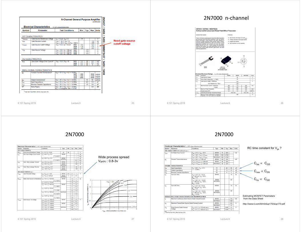
Lab 1 Notes Three Stage Amplifier – Crossover Distortion...
16
• Crossover Distortion •FETS • Spec sheets • Configurations • Applications 6.101 Spring 2019 Lecture 6 1 Acknowledgements: Neamen, Donald: Microelectronics Circuit Analysis and Design, 3 rd Edition Light Bulb Power 6.101 Spring 2019 Lecture 6 2 A light bulb designed for 6V DC or AC operation needs to be powered from the 12VAC power adapter. How does this circuit impact the life expectancy of the light bulb? Lab 1 Notes • Scope probe ground is tied to power ground (same as function generator ground). • For BW, remember 2 • High Q will limit high end of modulating signal • Double tuned circuit will result cut bandwidth in half. 6.101 Spring 2019 Lecture 6 3 6.101 Spring 2019 Lecture 5 4 Three Stage Amplifier – Crossover Distortion Hole Feedback
Transcript of Lab 1 Notes Three Stage Amplifier – Crossover Distortion...
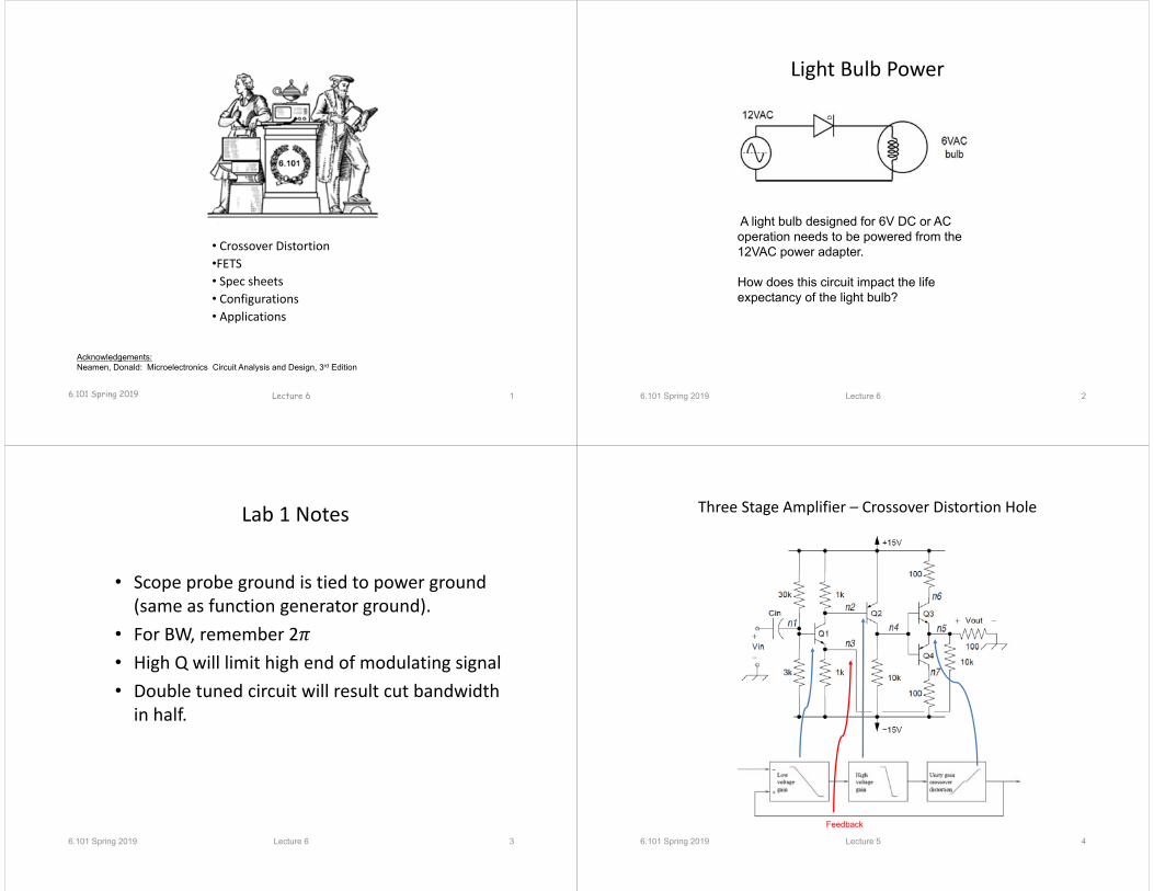
• Crossover Distortion•FETS• Spec sheets• Configurations• Applications
6.101 Spring 2019 Lecture 6 1
Acknowledgements: Neamen, Donald: Microelectronics Circuit Analysis and Design, 3rd Edition
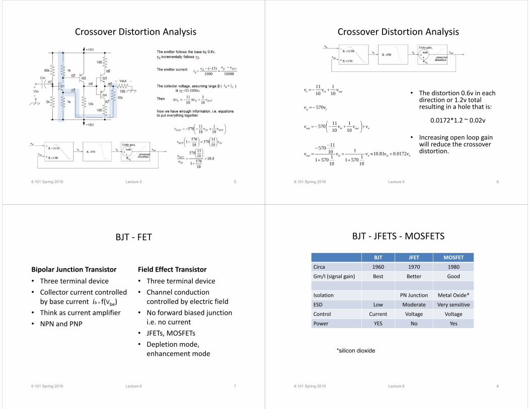
Light Bulb Power
6.101 Spring 2019 Lecture 6 2
A light bulb designed for 6V DC or AC operation needs to be powered from the 12VAC power adapter.
How does this circuit impact the life expectancy of the light bulb?
Lab 1 Notes
• Scope probe ground is tied to power ground (same as function generator ground).
• For BW, remember 2• High Q will limit high end of modulating signal• Double tuned circuit will result cut bandwidth in half.
6.101 Spring 2019 Lecture 6 3 6.101 Spring 2019 Lecture 5 4
Three Stage Amplifier – Crossover Distortion Hole
Feedback
Crossover Distortion Analysis
6.101 Spring 2019 Lecture 5 5
Crossover Distortion Analysis
6.101 Spring 2019 Lecture 5 6
ninninout
noutinout
eg
outine
vvvvv
vvvv
vv
vvv
0172.081.10
1015701
1
1015701
1011570
101
1011570
570
101
1011
• The distortion 0.6v in each direction or 1.2v total resulting in a hole that is:
0.0172*1.2 ~ 0.02v
• Increasing open loop gain will reduce the crossover distortion.
BJT ‐ FET
Bipolar Junction Transistor• Three terminal device• Collector current controlled
by base current ib = f(Vbe)• Think as current amplifier• NPN and PNP
Field Effect Transistor• Three terminal device• Channel conduction
controlled by electric field• No forward biased junction
i.e. no current• JFETs, MOSFETs• Depletion mode,
enhancement mode
6.101 Spring 2019 Lecture 6 7
BJT ‐ JFETS ‐MOSFETS
BJT JFET MOSFET
Circa 1960 1970 1980
Gm/I (signal gain) Best Better Good
Isolation PN Junction Metal Oxide*
ESD Low Moderate Very sensitive
Control Current Voltage Voltage
Power YES No Yes
6.101 Spring 2019 Lecture 6 8
*silicon dioxide

Voltage Noise *
6.101 Spring 2019 Lecture 6 9
* Horowitz & Hill, Art of Electronics 3rd Edition p 170
FET Family Tree
6.101 Spring 2019 Lecture 6 10
JFET
FET
enhancement
depletion
n-channel
MOSFET
p-channel depletion
n-channeln-channel p-channelVgs(off) gate source cutoff or
Vp pinch-off voltage Vgs(th) gate source threshold voltage
Transistor Polarity Mapping*
6.101 Spring 2019 Lecture 6 11
* Horwitz & Hill, the Art of Electronics, 3rd Edition
+
+
-
-p-channel enhancmentpnp bjt
n-channel enhancmentnpn bjt
p-channel JFT
n-channel depletionn-channel JFET
output
input
MOSFET & JFETS• MOSFETS
– Much more finicky difficult process (to make) than JFET’s.– Good news: Extremely high input impedance. Zero input current.– Bad news: Easily blown up by ESD on the gate. Add protection circuit
and input bias current becomes at best comparable to JFET’s.– Good news: Essentially infinitely fast. If you change the gate voltage,
the device will respond instantaneously! Essentially always in static equilibrium.
– Bad news: It can be really hard to change the gate voltage quickly! (especially power devices – BIG BIG capacitor)
– Much better power devices than JFET’s. (There were briefly power JFET’s as output devices in audio amps. Too many blew up.)
– And you can’t make digital VLSI out of JFET’s.
6.101 Spring 2019 Lecture 6 12

MOSFET vs JFETS
• JFET’s– Very simple manufacturing process like BJT’s. Much cheaper than
(discrete) MOSFET’s. Quieter than MOSFET’s. – Low input bias current – like back biased diode. As low as 10pA.– But note this doubles every 6 deg C! At high temps a JFET op amp can
have more input current than some bipolar op amps!– Used in microphones, hearing aids and other high impedance sources
(electret microphones have very high output impedance) because of low noise and ruggedness compared to MOSFET’s.
– Fast. Used on many high speed scope probes. Was major advance in bias current and speed over bipolar‐input op amps. See data sheets of (JFET input) LF356 series and compare to then bipolars.
– Downside is input capacitance can’t be as low as some BJT’s.– Wide spread in threshold voltage and zero‐Vgs current. Sometimes
requires sorting and selecting for a given circuit.
6.101 Spring 2019 Lecture 6 13
MOSFET Symbols
6.101 Spring 2019 Lecture 6 14
P-channelN-channel
IRFD9110
2N7000
S
S Bulk body terminal
6.101 Spring 2019 15
JFET: Junction FET Symbol
N channel JFET P channel JFET
G
D
S
G
D
S
G
D
S
G
D
S
6.101 Spring 2019 16
Simple Model of MOSFET
Vgs < Vt Vgs ≥ Vt
MOSFET made VSLI (microprocessors and memories) possible.
Very high input resistance Voltage controlled device ~25 V max operating
G
D
S
+Vgs -
G
D
S
G
D
S
off state on state
~0 gate current
2N7000 Ron 7.5 Ω@50ma
IRFD9110Ron 1.2 Ω@0.42A

W
L
MOSFETS: Gain & non‐linearitygate
drain
source
bulk
Inter-layer SiO2 insulation
Polysilicon wire
Doped (p-type or n-type) silicon substrate
Very thin (<20Å) high-quality SiO2insulating layer isolates gate from channel region.
Heavily doped (n-type or p-type) diffusions
Channel region: electric field from charges on gate locally “inverts” type of substrate to create a conducting channel between source and drain.
MOSFETs (metal-oxide-semiconductor field-effect transistors) are four-terminal voltage-controlled switches. Current flows between the diffusion terminals if the voltage on the gate terminal is large enough to create a conducting “channel”, otherwise the mosfet is off and the diffusion terminals are not connected.
IDS W/L
6.004 Chris Terman
FETs as switches
CONDUCTION:If a channel exists, a horizontal field will cause a drift current from the drain to the source.
Eh
gate
INVERSION:A sufficiently strong vertical field will attract enough electrons to the surface to create a conducting n-type channel between the source and drain. The gate voltage when the channel first forms is called the threshold voltage -- the mosfet switch goes from “off” to “on”.
Ev
inversionhappens here
The four terminals of a Field Effect Transistor (gate, source, drain and bulk) connect to conductors that generate a complicated set of electric fields in the channel region which depend on the relative voltages of each terminal.
p
N+ N+
source drain
bulk
6.004 Chris Terman
Four states of MOSFET for different Vgs and Vds
6.101 Spring 2019 Lecture 6 19
Olivier Deleage and Peter Scott (CC BY-SA 3.0)
What’s the difference between the drain and the source?
6.101 Spring 2019 Lecture 6 20
MOSFET’s can be symmetrical and drain and source interchangeable. Especially inside IC’s.
But discrete devices (with few exceptions) have input protection networks on the gate to protect against ESD. Also, the substrate must connect somewhere.
Once the input protection clamping and the substrate are connected to a terminal, that must be the source.

Classic “ideal” MOSFET characteristics –Flat curves in saturation region assume “long” channel
6.101 Spring 2019 Lecture 6 21
MOSFET BJT
“ideal” MOSFET curves continued
6.101 Spring 2019 Lecture 6 22
Triode mode, or “linear” mode, or ohmic region.
Saturation or active mode.
As the channel length becomes short, these equations become inaccurate.At the channel ends, source and drain regions causing “fringing” effects andDistort the electric fields from the “ideal” case used to derive above eq’s.
For analog design, long-channel MOSFET’s can offer extremely high outputImpedance, making excellent “stiff” current sources.Minimum geometry transistors used in digital VLSI do not have such flat curves.
Kn = transconductance parameter
Channel Length Modulation: Early Voltage
6.101 Spring 2019 Lecture 6 23 6.101 Spring 2019 Lecture 6 24
JFET p-channel
6.101 Spring 2019 Lecture 6 25
Need gate-source cutoff voltage
2N7000 n‐channel
6.101 Spring 2019 Lecture 6 26
2N7000
6.101 Spring 2019 Lecture 6 27
Wide process spreadVgs(th) : 0.8-3v
2N7000
6.101 Spring 2019 Lecture 6 28
Ciss CGS
Coss CDS
Cirs CGD
Estimating MOSFET Parameters from the Data Sheet
http://www.ti.com/lit/ml/slup170/slup170.pdf
RC time constant for Vgs ?
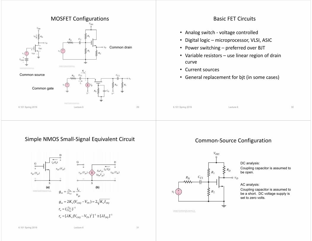
MOSFET Configurations
6.101 Spring 2019 Lecture 6 29
Common source
Common drain
Common gate
Basic FET Circuits
• Analog switch ‐ voltage controlled• Digital logic – microprocessor, VLSI, ASIC• Power switching – preferred over BJT• Variable resistors – use linear region of drain curve
• Current sources• General replacement for bjt (in some cases)
6.101 Spring 2019 Lecture 6 30
Simple NMOS Small‐Signal Equivalent Circuit
6.101 Spring 2019 Lecture 6 31
112
1
][])([
)(
2)(2
DQTNGSQno
vi
o
DQnTNGSQnm
gs
dvi
m
IVVKr
r
IKVVKg
vig
DS
D
GS
D
Common‐Source Configuration
DC analysis: Coupling capacitor is assumed to be open.
AC analysis: Coupling capacitor is assumed to be a short. DC voltage supply is set to zero volts.
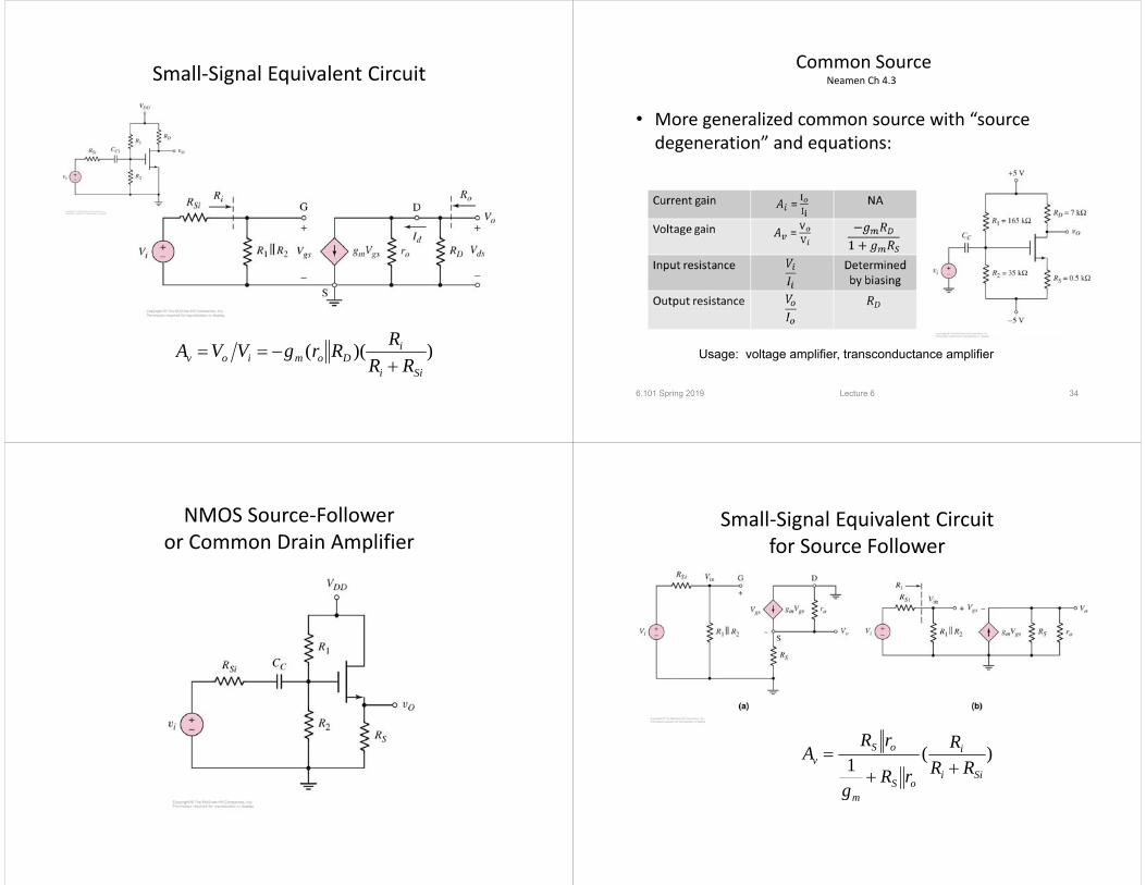
Small‐Signal Equivalent Circuit
))((Sii
iDomiov RR
RRrgVVA
Common SourceNeamen Ch 4.3
• More generalized common source with “source degeneration” and equations:
6.101 Spring 2019 Lecture 6 34
Usage: voltage amplifier, transconductance amplifier
NMOS Source‐Follower or Common Drain Amplifier
Small‐Signal Equivalent Circuit for Source Follower
)(1Sii
i
oSm
oSv RR
R
rRg
rRA
Common Drain – Source FollowerNeamen Ch 4.4
6.101 Spring 2019 Lecture 6 37
Usage: voltage buffer
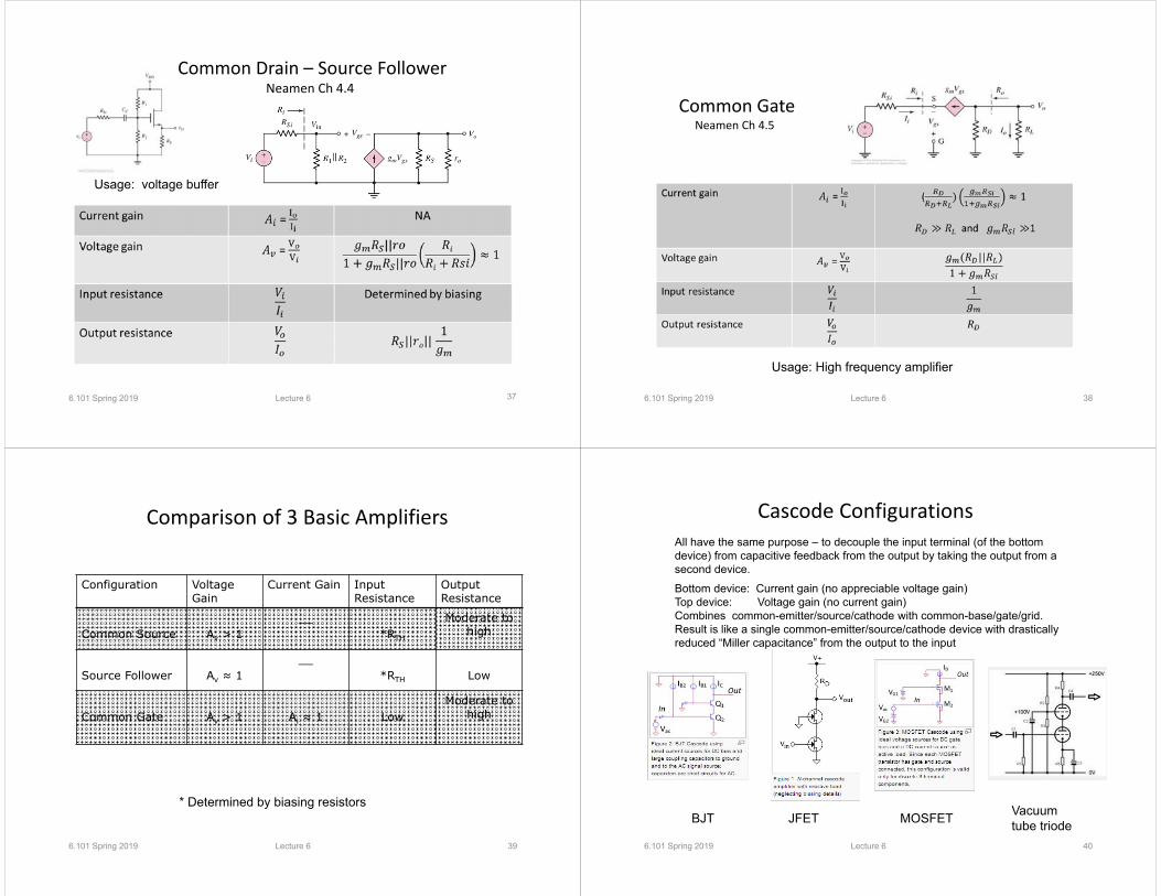
Common Gate Neamen Ch 4.5
6.101 Spring 2019 Lecture 6 38
Usage: High frequency amplifier
Comparison of 3 Basic Amplifiers
6.101 Spring 2019 Lecture 6 39
Configuration Voltage Gain
Current Gain Input Resistance
Output Resistance
Common Source Av > 1__
*RTH
Moderate to high
Source Follower Av ≈ 1__
*RTH Low
Common Gate Av > 1 Ai ≈ 1 LowModerate to
high
* Determined by biasing resistors
Cascode Configurations
6.101 Spring 2019 Lecture 6 40
BJT JFET MOSFET Vacuum tube triode
All have the same purpose – to decouple the input terminal (of the bottom device) from capacitive feedback from the output by taking the output from a second device.
Bottom device: Current gain (no appreciable voltage gain)Top device: Voltage gain (no current gain)Combines common-emitter/source/cathode with common-base/gate/grid. Result is like a single common-emitter/source/cathode device with drastically reduced “Miller capacitance” from the output to the input
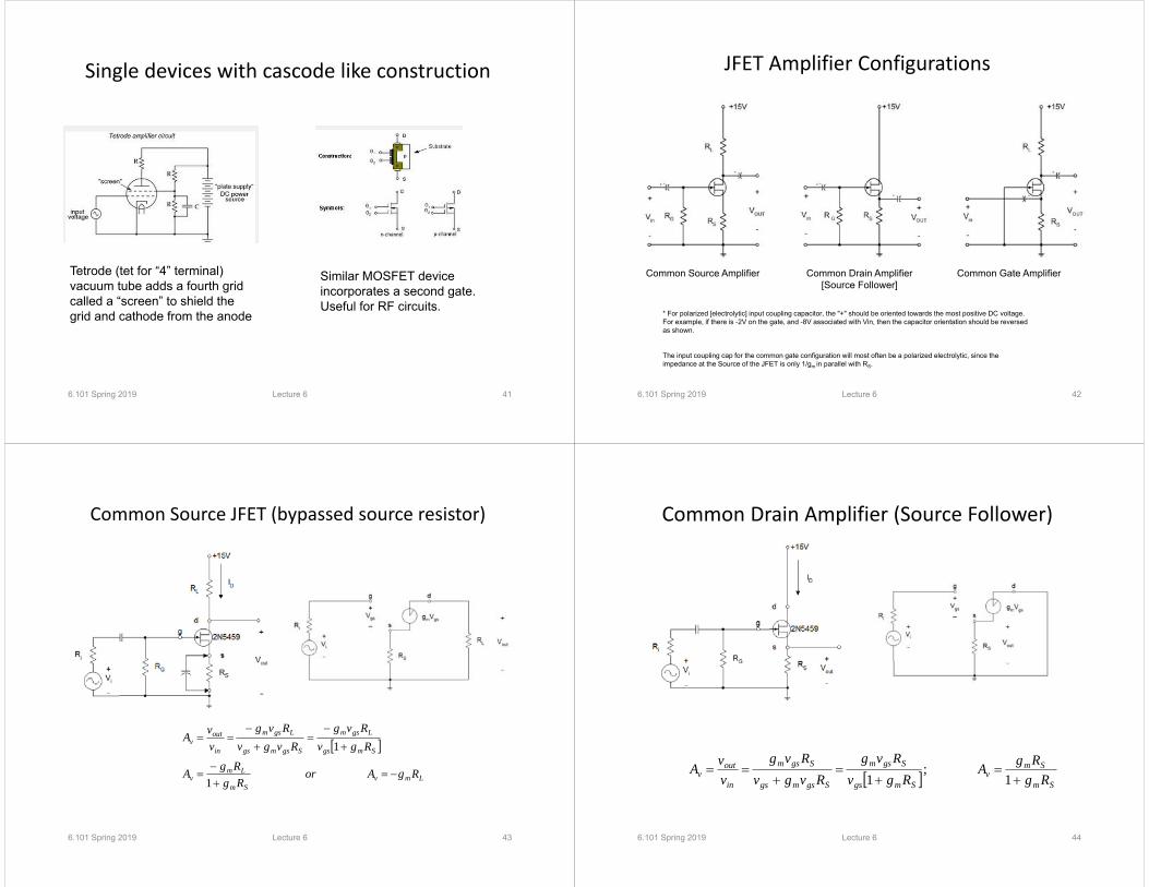
Single devices with cascode like construction
6.101 Spring 2019 Lecture 6 41
Tetrode (tet for “4” terminal) vacuum tube adds a fourth grid called a “screen” to shield the grid and cathode from the anode
Similar MOSFET device incorporates a second gate. Useful for RF circuits.
JFET Amplifier Configurations
6.101 Spring 2019 Lecture 6 42
* For polarized [electrolytic] input coupling capacitor, the "+" should be oriented towards the most positive DC voltage. For example, if there is -2V on the gate, and -8V associated with Vin, then the capacitor orientation should be reversed as shown.
The input coupling cap for the common gate configuration will most often be a polarized electrolytic, since the impedance at the Source of the JFET is only 1/gm in parallel with RS.
Common Source Amplifier Common Gate AmplifierCommon Drain Amplifier[Source Follower]
Common Source JFET (bypassed source resistor)
6.101 Spring 2019 Lecture 6 43
LmvSm
Lmv
Smgs
Lgsm
Sgsmgs
Lgsm
in
outv
RgAorRgRgA
RgvRvg
RvgvRvg
vvA
1
1
Common Drain Amplifier (Source Follower)
6.101 Spring 2019 Lecture 6 44
Sm
Smv
Smgs
Sgsm
Sgsmgs
Sgsm
in
outv Rg
RgARgv
RvgRvgv
RvgvvA
1;
1
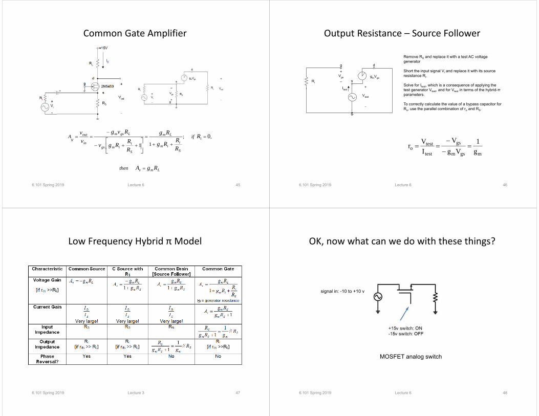
Common Gate Amplifier
6.101 Spring 2019 Lecture 6 45
Lmv
i
S
iim
Lm
S
iimgs
Lgsm
in
out
RgA
R
RRRg
Rg
RRRgv
Rvgvv
then
ifvA
,;
11
0
Output Resistance – Source Follower
6.101 Spring 2019 Lecture 6 46
Ri
gmVgs
+
Vtest
_
g
+Vgs_
d
s
Itest
Remove RS and replace it with a test AC voltage generator
Short the input signal Vi and replace it with its source resistance Ri.
Solve for Itest, which is a consequence of applying the test generator Vtest, and for Vtest in terms of the hybrid-π parameters.
To correctly calculate the value of a bypass capacitor for Rs, use the parallel combination of ro and RS.
mgsm
gs
test
testo g
1Vg
VIVr
Low Frequency Hybrid πModel
6.101 Spring 2019 Lecture 3 47
OK, now what can we do with these things?
6.101 Spring 2019 Lecture 6 48
MOSFET analog switch
signal in: -10 to +10 v
OK, now what can we do with these things?
6.101 Spring 2019 Lecture 6 49
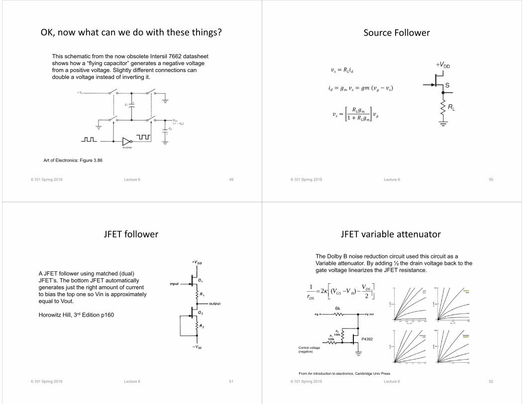
This schematic from the now obsolete Intersil 7662 datasheet shows how a “flying capacitor” generates a negative voltage from a positive voltage. Slightly different connections can double a voltage instead of inverting it.
Art of Electronics: Figure 3.86
6.101 Spring 2019 Lecture 6 50
Source Follower
1
JFET follower
6.101 Spring 2019 Lecture 6 51
A JFET follower using matched (dual) JFET’s. The bottom JFET automatically generates just the right amount of current to bias the top one so Vin is approximately equal to Vout.
Horowitz Hill, 3rd Edition p160
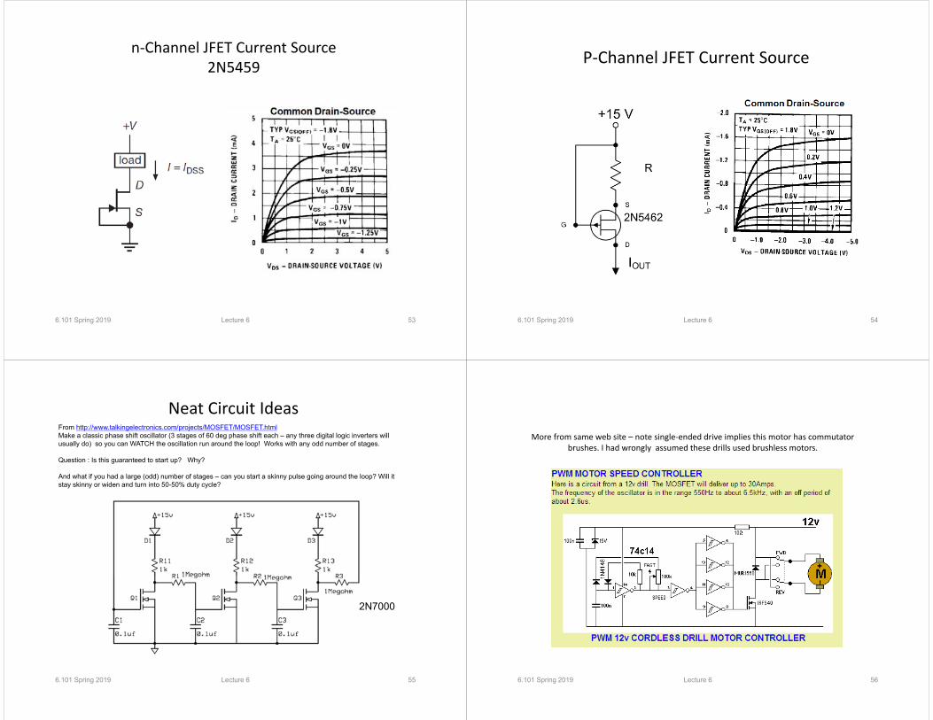
JFET variable attenuator
6.101 Spring 2019 Lecture 6 52
The Dolby B noise reduction circuit used this circuit as aVariable attenuator. By adding ½ the drain voltage back to the gate voltage linearizes the JFET resistance.
From An introduction to electronics, Cambridge Univ Press
2)(21 DS
thGSDS
VVVr
Control voltage(negative)
6k6k
P4392
n‐Channel JFET Current Source2N5459
6.101 Spring 2019 Lecture 6 53
P‐Channel JFET Current Source
6.101 Spring 2019 Lecture 6 54
Neat Circuit Ideas
6.101 Spring 2019 Lecture 6 55
From http://www.talkingelectronics.com/projects/MOSFET/MOSFET.htmlMake a classic phase shift oscillator (3 stages of 60 deg phase shift each – any three digital logic inverters will usually do) so you can WATCH the oscillation run around the loop! Works with any odd number of stages.
Question : Is this guaranteed to start up? Why?
And what if you had a large (odd) number of stages – can you start a skinny pulse going around the loop? Will it stay skinny or widen and turn into 50-50% duty cycle?
2N7000
More from same web site – note single‐ended drive implies this motor has commutatorbrushes. I had wrongly assumed these drills used brushless motors.
6.101 Spring 2019 Lecture 6 56
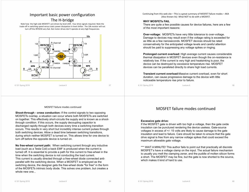
Important basic power configurationThe H‐bridge
Note how the high‐side MOSFET’s are driven by level shift. Four drive signals required. Note the trade‐off in switching speed versus static power dissipation in level shifter. The 10k resistor will not
turn off the IRF9Z30 very fast. But motor drives don’t operate at very high frequencies.
6.101 Spring 2019 Lecture 6 57
Continuing from this web site – This is a great summary of MOSFET failure modes – AKA (Also Known As) What NOT to do with a MOSFET.
6.101 Spring 2019 Lecture 6 58
WHY MOSFETs FAILThere are quite a few possible causes for device failures, here are a few of the most important reasons:
Over-voltage: MOSFETs have very little tolerance to over-voltage. Damage to devices may result even if the voltage rating is exceeded for as little as a few nanoseconds. MOSFET devices should be rated conservatively for the anticipated voltage levels and careful attention should be paid to suppressing any voltage spikes or ringing.
Prolonged current overload: High average current causes considerable thermal dissipation in MOSFET devices even though the on-resistance is relatively low. If the current is very high and heatsinking is poor, the device can be destroyed by excessive temperature rise. MOSFET devices can be paralleled directly to share high load currents.
Transient current overload:Massive current overload, even for short duration, can cause progressive damage to the device with little noticeable temperature rise prior to failure.
MOSFET failure modes continued
6.101 Spring 2019 Lecture 6 59
Shoot-through - cross conduction: If the control signals to two opposing MOSFETs overlap, a situation can occur where both MOSFETs are switched on together. This effectively short-circuits the supply and is known as a shoot-through condition. If this occurs, the supply decoupling capacitor is discharged rapidly through both devices every time a switching transition occurs. This results in very short but incredibly intense current pulses through both switching devices. Allow a dead time between switching transitions, during which neither MOSFET is turned on. This allows time for one device to turn off before the opposite device is turned on.
No free-wheel current path: When switching current through any inductive load (such as a Tesla Coil) a back EMF is produced when the current is turned off. It is essential to provide a path for this current to free-wheel in the time when the switching device is not conducting the load current.This current is usually directed through a free-wheel diode connected anti-parallel with the switching device. When a MOSFET is employed as the switching device, the designer gets the free-wheel diode "for free" in the form of the MOSFETs intrinsic body diode. This solves one problem, but creates a whole new one...
MOSFET failure modes continued
6.101 Spring 2019 Lecture 6 60
Excessive gate drive:If the MOSFET gate is driven with too high a voltage, then the gate oxide insulation can be punctured rendering the device useless. Gate-source voltages in excess of +/- 15 volts are likely to cause damage to the gate insulation and lead to failure. Care should be taken to ensure that the gate drive signal is free from any narrow voltage spikes that could exceed the maximum allowable gate voltage.
*** WAIT A MINUTE! This author fails to point out that practically all discrete MOSFET’s have a voltage clamp on the input. The actual failure mechanism is usually you melt the clamping zener, and the puddle of molten silicon forms a short. The MOSFET may be fine, but the gate is now shorted to the source, which makes it kind of hard to use.

MOSFET failure modes continued
6.101 Spring 2019 Lecture 6 61
Insufficient gate drive - incomplete turn on:MOSFET devices are only capable of switching large amounts of power because they are designed to dissipate minimal power when they are turned on. It is the responsibility of the designer to ensure that the MOSFET device is turned hard on to minimise dissipation during conduction. If the device is not fully turned on then the device will have a high resistance during conduction and will dissipate considerable power as heat. A gate voltage of between 10 and 15 volts ensures full turn-on with most MOSFET devices.
***NOTE: The reference to gate voltages of “between 10 and 15 volts” applies to older or higher voltage power devices (like 20 to 200V). The newer power parts have long been based on the latest digital process: i.e., they’re designed for 5V. Newer power MOSFET’s have guaranteed on resistance at lower Vgs voltages consistent with use in 3.3V logic inputs, and have Vdsabsolute maximum ratings of 6V or 7V, and similar abs max Vgs ratings. Modern logic requires lots of power conversion devices operating at these low voltages.
For further reading and possible inspiration for your projects, read Jim Williams app notes! You gotta love a guy who titles an app note (#25) :
6.101 Spring 2019 Lecture 6 62
The above title is not happenstance and was arrived at after considerable deliberation… Mysterious modes, sudden, seemingly inexplicable failures, peculiar regulation characteristics and just plain explosions are common occurrences. Diodes conduct the wrong way. Things get hot that shouldn’t. Capacitors act like resistors, fuses don’t blow and transistors do. The output is at ground, and the ground terminal shows volts of noise. Added to this poisonous brew is the regulator’s feedback loop, sampled in nature and replete with uncertain phase shifts. Everything, of course, varies with line and load conditions— and the time of day, or so it seems. In the face of such menace, what are Everyman and the poets to do?
6.101 Spring 2019 Lecture 6 63 6.101 Spring 2019 Lecture 6 64