L15 – Testing 1 6.884 – Spring 2005 Krste, 3/16/05 Verification and Testing He’s dead Jim...
29
L15 – Testing 1 6.884 – Spring 2005 Krste, 3/16/05 Verification and Testing He’s dead Jim...
-
Upload
monica-wells -
Category
Documents
-
view
213 -
download
0
Transcript of L15 – Testing 1 6.884 – Spring 2005 Krste, 3/16/05 Verification and Testing He’s dead Jim...

L15 – Testing 16.884 – Spring 2005 Krste, 3/16/05
Verification and Testing
He’s dead Jim...

L15 – Testing 26.884 – Spring 2005 Krste, 3/16/05
Verification versus Manufacturing Test
Design verification determines whether your design correctly implements a specification
…and hopefully that the specification was correct
Manufacturing tests determine whether the fabrication process successfully reproduced an instance of your design with acceptable quality– Quality measures include operating frequency,
power consumption, and expected operating lifetime
– Modern manufacturing test is impossible without on-chip test structures: testability is part of design specification

L15 – Testing 36.884 – Spring 2005 Krste, 3/16/05
Design Verification Philosophy
If you haven’t verified it, it doesn’t work!
Verification should be treated as an intrinsic part of the design process– not as an independent activity to be handled by lesser
mortals after the “genius” designers have finished their “masterpiece”
– Verification infrastructure often represents the “crown jewels” of a successful chip design company (e.g., Intel x86 spec.)
Verification infrastructure should be available before design– Verification tests are the de facto specification of the
part– In your projects, you will write tests first!
L15 – Testing 46.884 – Spring 2005 Krste, 3/16/05
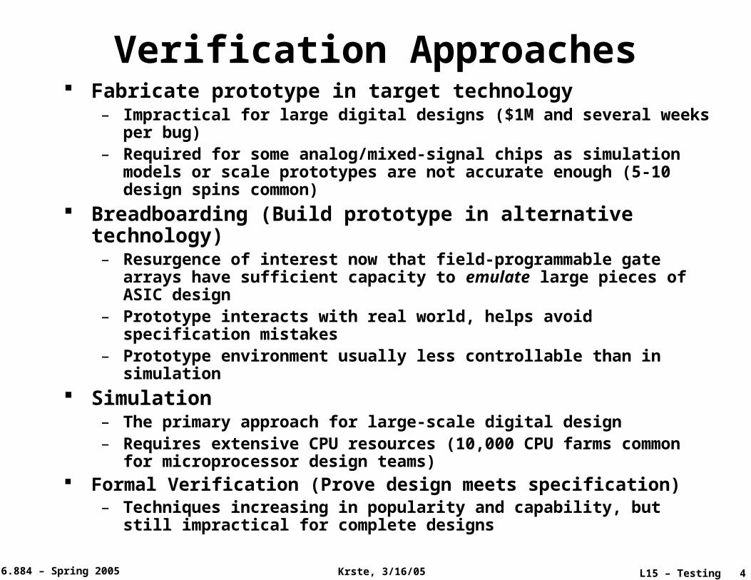
Verification Approaches Fabricate prototype in target technology
– Impractical for large digital designs ($1M and several weeks per bug)
– Required for some analog/mixed-signal chips as simulation models or scale prototypes are not accurate enough (5-10 design spins common)
Breadboarding (Build prototype in alternative technology)– Resurgence of interest now that field-programmable gate
arrays have sufficient capacity to emulate large pieces of ASIC design
– Prototype interacts with real world, helps avoid specification mistakes
– Prototype environment usually less controllable than in simulation
Simulation– The primary approach for large-scale digital design– Requires extensive CPU resources (10,000 CPU farms
common for microprocessor design teams) Formal Verification (Prove design meets specification)
– Techniques increasing in popularity and capability, but still impractical for complete designs
L15 – Testing 56.884 – Spring 2005 Krste, 3/16/05
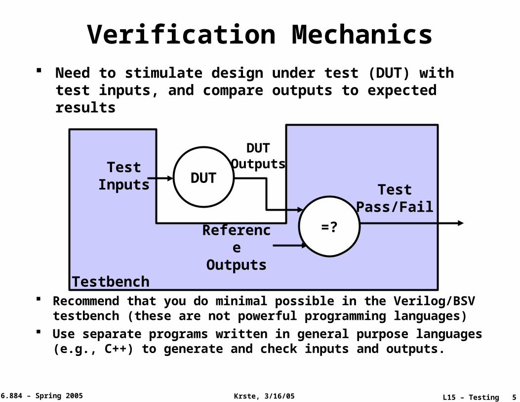
Testbench
Verification Mechanics Need to stimulate design under test (DUT) with
test inputs, and compare outputs to expected results
DUTTest
Inputs
DUT Output
s
=?Reference
Outputs
Test Pass/Fail
Recommend that you do minimal possible in the Verilog/BSV testbench (these are not powerful programming languages)
Use separate programs written in general purpose languages (e.g., C++) to generate and check inputs and outputs.
L15 – Testing 66.884 – Spring 2005 Krste, 3/16/05
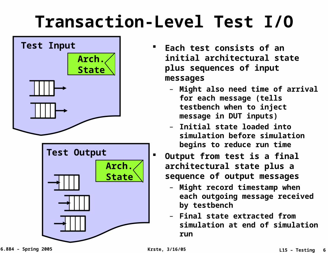
Transaction-Level Test I/O Each test consists of an initial
architectural state plus sequences of input messages– Might also need time of arrival
for each message (tells testbench when to inject message in DUT inputs)
– Initial state loaded into simulation before simulation begins to reduce run time
Output from test is a final architectural state plus a sequence of output messages– Might record timestamp when
each outgoing message received by testbench
– Final state extracted from simulation at end of simulation run
Arch. State
Test Input
Arch. State
Test Output

L15 – Testing 76.884 – Spring 2005 Krste, 3/16/05
Checking Outputs Use separate checker program to compare outputs
– Can be complicated to compare outputs in some cases (e.g., if output messages can be reordered)
DUT
Test Inputs Checker
Test Pass/Fail
Golden
Output
UTLGoldenModel
DUT Output
s
DUT
Test Inputs Checker
Test Pass/Fail
DUT Output
s
Can use UTL model to generate reference output stream. This can be simpler than building all intelligence into output checker.
Optional
L15 – Testing 86.884 – Spring 2005 Krste, 3/16/05
Types of Test
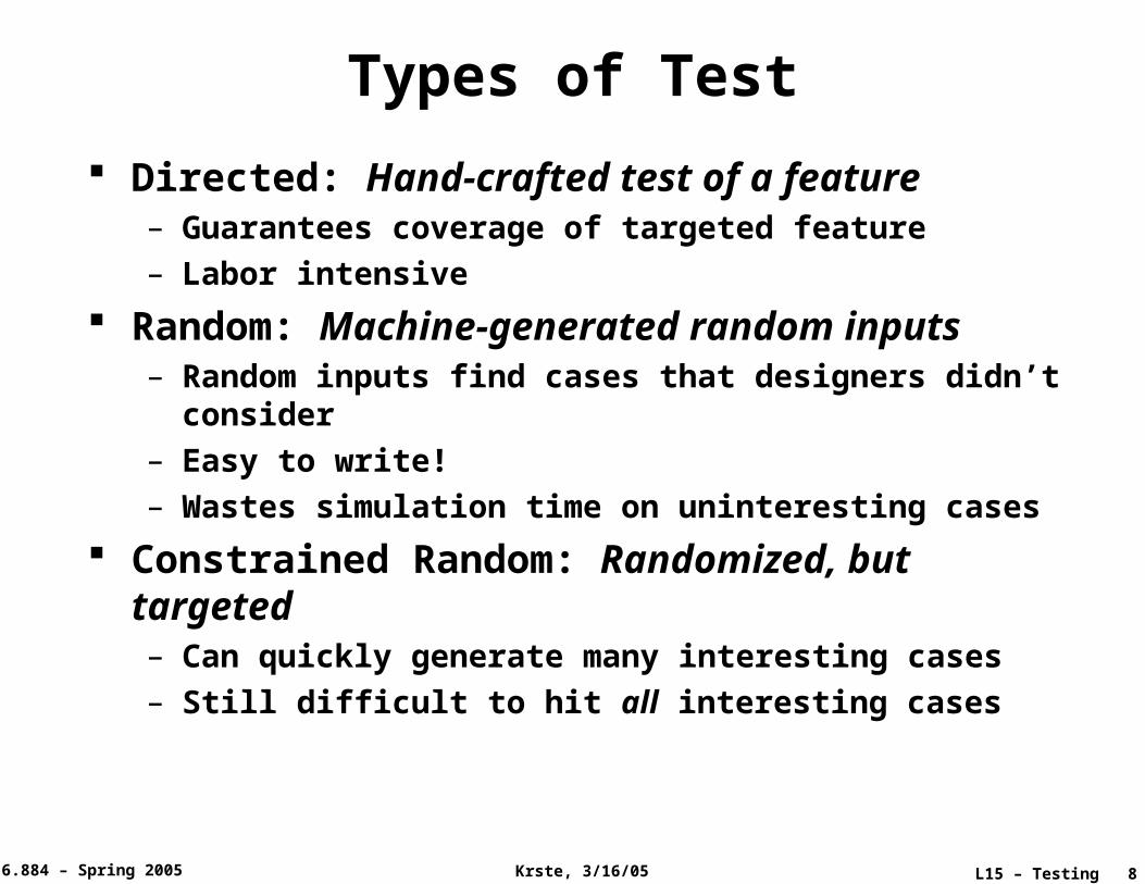
Directed: Hand-crafted test of a feature– Guarantees coverage of targeted feature– Labor intensive
Random: Machine-generated random inputs– Random inputs find cases that designers didn’t
consider– Easy to write!– Wastes simulation time on uninteresting cases
Constrained Random: Randomized, but targeted– Can quickly generate many interesting cases– Still difficult to hit all interesting cases
L15 – Testing 96.884 – Spring 2005 Krste, 3/16/05
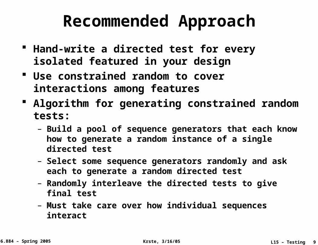
Recommended Approach
Hand-write a directed test for every isolated featured in your design
Use constrained random to cover interactions among features
Algorithm for generating constrained random tests:– Build a pool of sequence generators that each know
how to generate a random instance of a single directed test
– Select some sequence generators randomly and ask each to generate a random directed test
– Randomly interleave the directed tests to give final test
– Must take care over how individual sequences interact
L15 – Testing 106.884 – Spring 2005 Krste, 3/16/05
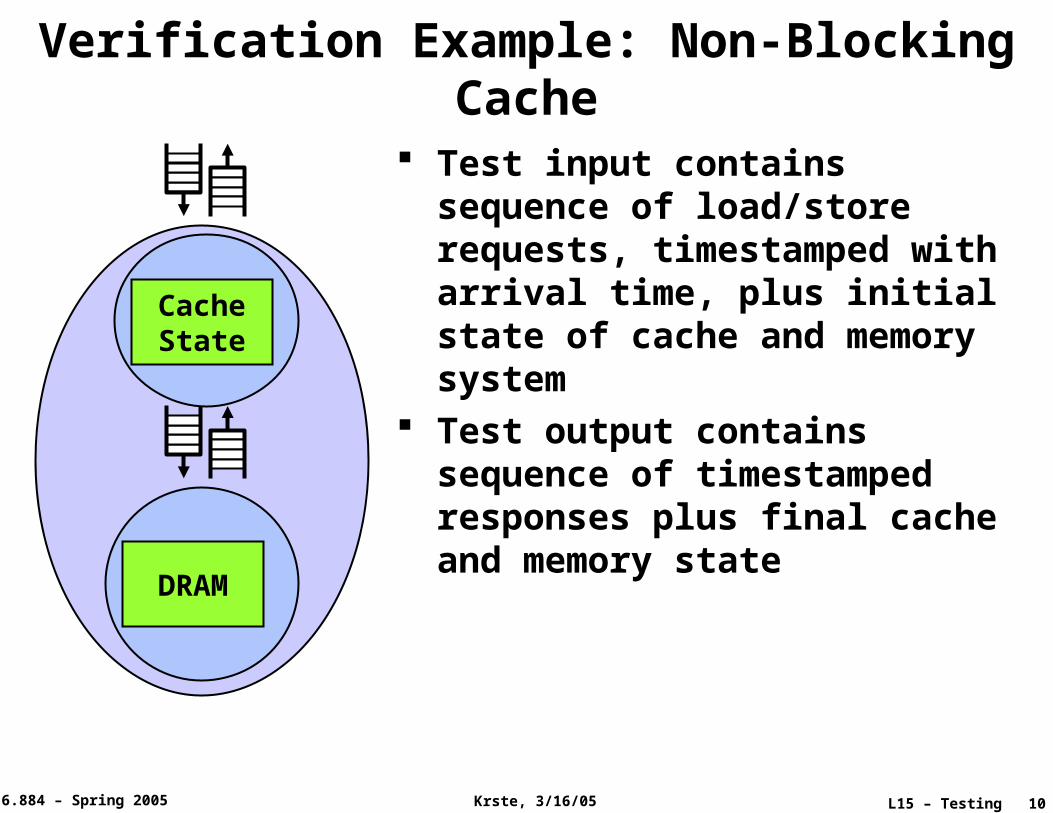
Verification Example: Non-Blocking Cache
Test input contains sequence of load/store requests, timestamped with arrival time, plus initial state of cache and memory system
Test output contains sequence of timestamped responses plus final cache and memory state
DRAM
Cache State
L15 – Testing 116.884 – Spring 2005 Krste, 3/16/05
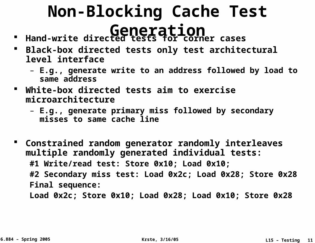
Non-Blocking Cache Test Generation Hand-write directed tests for corner cases
Black-box directed tests only test architectural level interface– E.g., generate write to an address followed by load to
same address White-box directed tests aim to exercise
microarchitecture– E.g., generate primary miss followed by secondary misses
to same cache line
Constrained random generator randomly interleaves multiple randomly generated individual tests:#1 Write/read test: Store 0x10; Load 0x10;#2 Secondary miss test: Load 0x2c; Load 0x28; Store 0x28Final sequence:Load 0x2c; Store 0x10; Load 0x28; Load 0x10; Store 0x28
L15 – Testing 126.884 – Spring 2005 Krste, 3/16/05
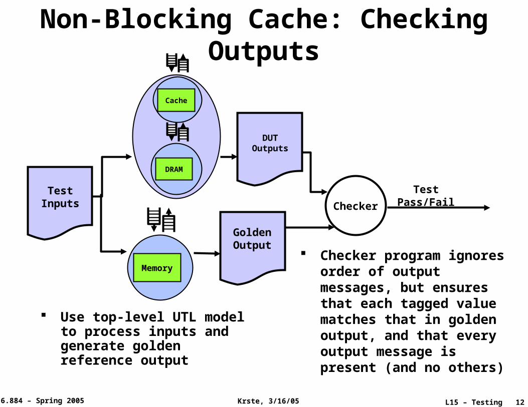
Non-Blocking Cache: Checking Outputs
Checker program ignores order of output messages, but ensures that each tagged value matches that in golden output, and that every output message is present (and no others)
Memory
Test Inputs
Test Pass/Fail
Golden Output
DUT Outputs
DRAM
Cache
Use top-level UTL model to process inputs and generate golden reference output
Checker

L15 – Testing 136.884 – Spring 2005 Krste, 3/16/05
Test Coverage Important to quantify effectiveness of the
verification strategy. Simply running lots of cycles isn’t enough.
Simulator can help by determining how much of the design is exercised when running test suite– Have all wires been toggled?– Have all state machine transitions occurred?– Have all Bluespec rules fired? All lines of Verilog
executed? Bare minimum is that all parts of design have
been exercised, but this is not enough– Would an error be observed in test output if this
logic didn’t respond correctly?– Can inject faults into design to test verification
suite, but this is computationally expensive– Many industry teams plot bugs found over time then
tapeout when rate of finding bugs slows down (doesn’t mean there aren’t lots of bugs left, might be they’re not being found!)

L15 – Testing 146.884 – Spring 2005 Krste, 3/16/05
Goal: verify every gate is operating as expected
Defects from misalignment, dust and other particles, “stacking” faults, pinholes in dielectrics, mask scratches & dirt, thickness variations, layer-to-layer shorts, discontinuous wires (“opens”), circuit sensitivities (VTH, LCHANNEL). Find during wafer probe of test structures.
Defects from scratching in handling, damage during bonding to lead frame, mfg defects undetected during wafer probe (particularly speed-related problems). Find during testing of packaged parts.
Defects from damage during board insertion (thermal, ESD), infant mortality (mfg defects that show up after a few hours of use). Alsonoise problems, susceptibility to latch-up, ...Find during testing/burn-in of boards.
Defects that only appear after months or years of use (metal migration, oxide damage during manufacture, impurities).Found by customer (oops!).
Cost of replacing defective component increasesby an order of magnitude with each stage ofmanufacture.
Cost of replacing defective component increasesby an order of magnitude with each stage ofmanufacture.
Manufacturing Defects
L15 – Testing 156.884 – Spring 2005 Krste, 3/16/05
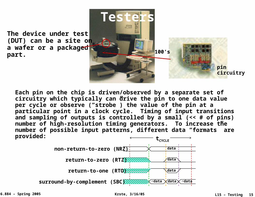
The device under test(DUT) can be a site ona wafer or a packagedpart.
Each pin on the chip is driven/observed by a separate set of circuitry which typically can drive the pin to one data value per cycle or observe (“strobe”) the value of the pin at a particular point in a clock cycle. Timing of input transitions and sampling of outputs is controlled by a small (<< # of pins) number of high-resolution timing generators. To increase the number of possible input patterns, different data “formats” are provided:
tCYCLE
non-return-to-zero (NRZ)
return-to-zero (RTZ)
return-to-one (RTO)
surround-by-complement (SBC)
data
data
data
data ~data~data
pincircuitry
100’s
Testers

L15 – Testing 166.884 – Spring 2005 Krste, 3/16/05
Plan: supply a set of test vectors that specify an input or output value for every pin on every cycle. Tester will load the program into the pin cards, run it and report any miscompares between an observed output value and the expected value.
0000 1 10 0000 XXXX0001 1 10 0000 LLLL0002 1 01 1111 LLLL0003 1 00 1011 HLHL
cycle # program for 11 pins
input to chip = {0, 1}output from chip = {L, H}tristate/no compare = { X }
How many vectors do we need?Exhaustive testing is not only impractical, it’s unnecessary! Instead we only need to verify that no faults are present which may take many fewer vectors.
combinationallogic
n
2n inputs required toexhaustively test circuit
combinationallogic
n
m m
2n+m inputs required toexhaustively test circuit
If n=25, m=50, 1us/testthen test time > 109 years
Testing Approaches
L15 – Testing 176.884 – Spring 2005 Krste, 3/16/05
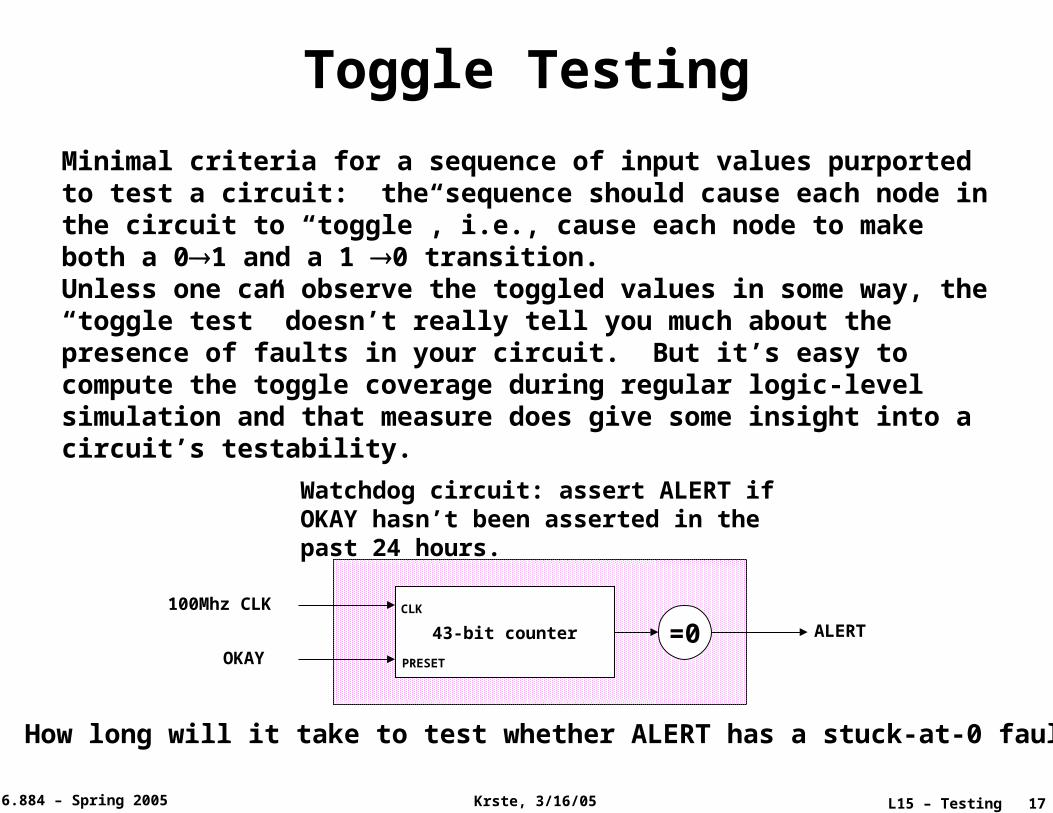
Minimal criteria for a sequence of input values purported to test a circuit: the sequence should cause each node in the circuit to “toggle”, i.e., cause each node to make both a 01 and a 1 0 transition.Unless one can observe the toggled values in some way, the “toggle test” doesn’t really tell you much about the presence of faults in your circuit. But it’s easy to compute the toggle coverage during regular logic-level simulation and that measure does give some insight into a circuit’s testability.
Watchdog circuit: assert ALERT if OKAY hasn’t been asserted in the past 24 hours.
100Mhz CLK
OKAY
ALERT43-bit counter =0CLK
PRESET
How long will it take to test whether ALERT has a stuck-at-0 fault?
Toggle Testing

L15 – Testing 186.884 – Spring 2005 Krste, 3/16/05
Traditional model, first developed for board-level tests, assumes that a node gets “stuck” at a “0” or “1”, presumably by shorting to GND or VDD.
X
stuck at “0” = S-A-0 = node@0stuck at “1” = S-A-1 = node@1
ABCD
Z = ABCDZB@1 = ACDZB@0 = 0 = Z@0
Two faults are equivalent iftheir effects on the circuit areindistinguishable.
One can fault an entire node or just a single connection (which would correspond to a transistor stuck-on or stuck-off).
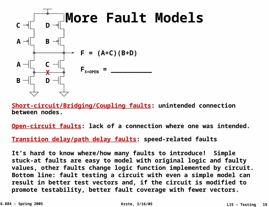
In CMOS, stuck-on andstuck-off faults canhave interestingconsequences... A
B
X
F = ABFX=OPEN=_______
Fault Models
L15 – Testing 196.884 – Spring 2005 Krste, 3/16/05
A
B
BA
DC
D
CX
F = (A+C)(B+D)
FX=OPEN = __________
Short-circuit/Bridging/Coupling faults: unintended connection between nodes.
Open-circuit faults: lack of a connection where one was intended.
Transition delay/path delay faults: speed-related faults
It’s hard to know where/how many faults to introduce! Simple stuck-at faults are easy to model with original logic and faulty values, other faults change logic function implemented by circuit. Bottom line: fault testing a circuit with even a simple model can result in better test vectors and, if the circuit is modified to promote testability, better fault coverage with fewer vectors.
More Fault Models
L15 – Testing 206.884 – Spring 2005 Krste, 3/16/05
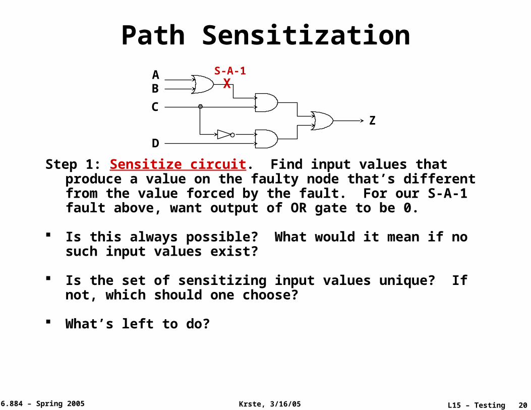
XAB
C
D
Z
S-A-1
Path Sensitization
Step 1: Sensitize circuit. Find input values that produce a value on the faulty node that’s different from the value forced by the fault. For our S-A-1 fault above, want output of OR gate to be 0.
Is this always possible? What would it mean if no such input values exist?
Is the set of sensitizing input values unique? If not, which should one choose?
What’s left to do?
L15 – Testing 216.884 – Spring 2005 Krste, 3/16/05
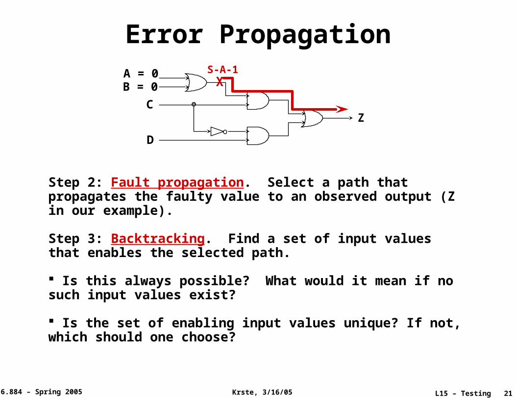
XA = 0B = 0
C
D
Z
S-A-1
Step 2: Fault propagation. Select a path that propagates the faulty value to an observed output (Z in our example).
Step 3: Backtracking. Find a set of input values that enables the selected path.
Is this always possible? What would it mean if no such input values exist?
Is the set of enabling input values unique? If not, which should one choose?
Error Propagation
L15 – Testing 226.884 – Spring 2005 Krste, 3/16/05
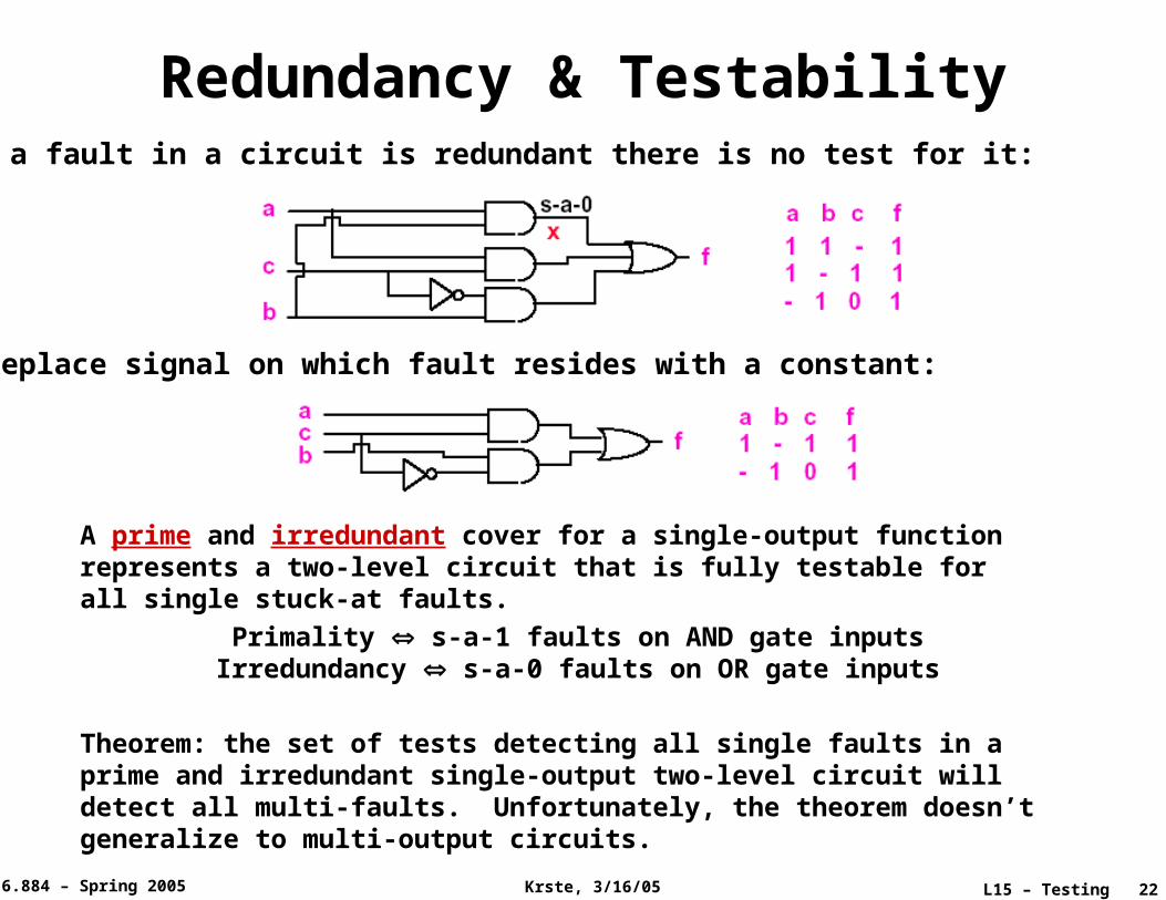
If a fault in a circuit is redundant there is no test for it:
Replace signal on which fault resides with a constant:
A prime and irredundant cover for a single-output function represents a two-level circuit that is fully testable for all single stuck-at faults.
Primality s-a-1 faults on AND gate inputsIrredundancy s-a-0 faults on OR gate inputs
Theorem: the set of tests detecting all single faults in a prime and irredundant single-output two-level circuit will detect all multi-faults. Unfortunately, the theorem doesn’t generalize to multi-output circuits.
Redundancy & Testability
L15 – Testing 236.884 – Spring 2005 Krste, 3/16/05
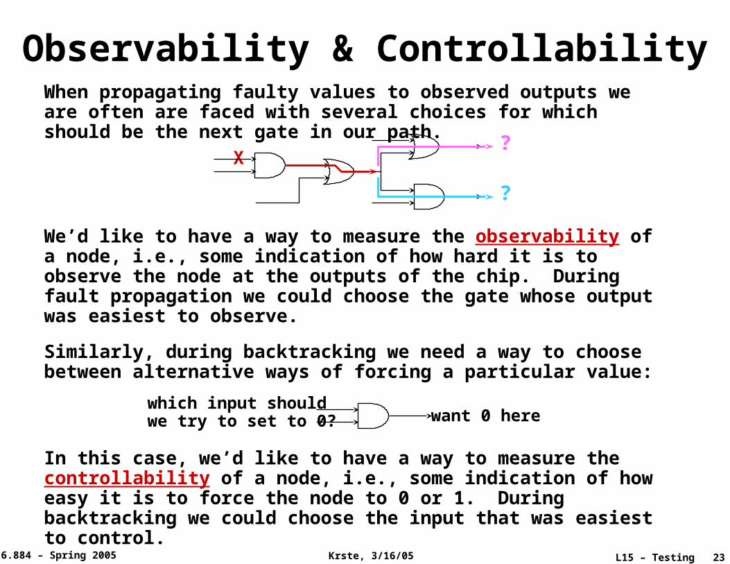
When propagating faulty values to observed outputs we are often are faced with several choices for which should be the next gate in our path.
X?
?
We’d like to have a way to measure the observability of a node, i.e., some indication of how hard it is to observe the node at the outputs of the chip. During fault propagation we could choose the gate whose output was easiest to observe.
Similarly, during backtracking we need a way to choose between alternative ways of forcing a particular value:
want 0 herewhich input shouldwe try to set to 0?
In this case, we’d like to have a way to measure the controllability of a node, i.e., some indication of how easy it is to force the node to 0 or 1. During backtracking we could choose the input that was easiest to control.
Observability & Controllability

L15 – Testing 246.884 – Spring 2005 Krste, 3/16/05
What can we do to increase testability?
increase observability ð add more pins (?!) ð add small “probe” bus, selectively enable different values onto bus ð use a hash function to “compress” a sequence of values (e.g., the values of a bus over many clock cycles) into a small number of bits for later read-out ð cheap read-out of all state information
increase controllability ð use muxes to isolate submodules and select sources of test data as inputs ð provide easy setup of internal state
There are systematic techniques:
scan-based approaches built-in self-test (BIST) signature analysis
There are systematic techniques:
scan-based approaches built-in self-test (BIST) signature analysis
Design For Test
L15 – Testing 256.884 – Spring 2005 Krste, 3/16/05
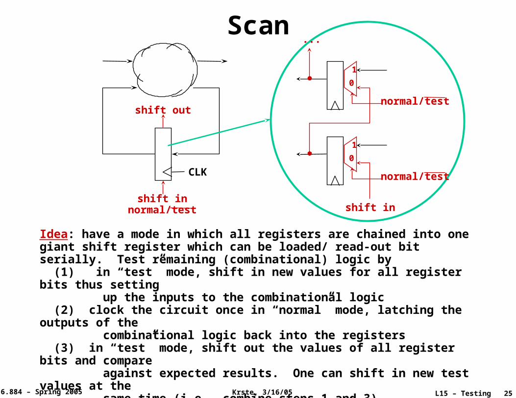
Idea: have a mode in which all registers are chained into one giant shift register which can be loaded/ read-out bit serially. Test remaining (combinational) logic by (1) in “test” mode, shift in new values for all register bits thus setting up the inputs to the combinational logic (2) clock the circuit once in “normal” mode, latching the outputs of the combinational logic back into the registers (3) in “test” mode, shift out the values of all register bits and compare against expected results. One can shift in new test values at the same time (i.e., combine steps 1 and 3).
CLK
shift innormal/test
shift out
1
0
normal/test
shift in
1
0
normal/test
...Scan
L15 – Testing 266.884 – Spring 2005 Krste, 3/16/05
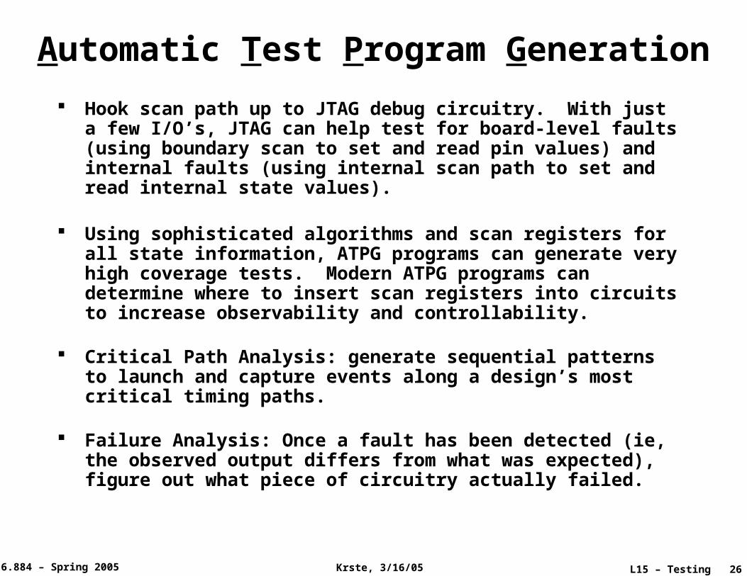
Automatic Test Program Generation
Hook scan path up to JTAG debug circuitry. With just a few I/O’s, JTAG can help test for board-level faults (using boundary scan to set and read pin values) and internal faults (using internal scan path to set and read internal state values).
Using sophisticated algorithms and scan registers for all state information, ATPG programs can generate very high coverage tests. Modern ATPG programs can determine where to insert scan registers into circuits to increase observability and controllability.
Critical Path Analysis: generate sequential patterns to launch and capture events along a design’s most critical timing paths.
Failure Analysis: Once a fault has been detected (ie, the observed output differs from what was expected), figure out what piece of circuitry actually failed.
L15 – Testing 276.884 – Spring 2005 Krste, 3/16/05
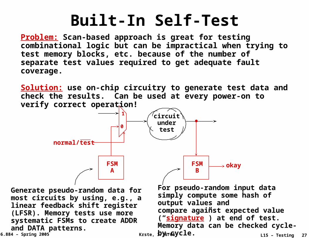
Problem: Scan-based approach is great for testing combinational logic but can be impractical when trying to test memory blocks, etc. because of the number of separate test values required to get adequate fault coverage.
Solution: use on-chip circuitry to generate test data and check the results. Can be used at every power-on to verify correct operation!
normal/test
1
0
FSMA
FSMB
okay
circuitundertest
Generate pseudo-random data for most circuits by using, e.g., a linear feedback shift register (LFSR). Memory tests use more systematic FSMs to create ADDR and DATA patterns.
For pseudo-random input data simply compute some hash of output values andcompare against expected value (“signature”) at end of test. Memory data can be checked cycle-by-cycle.
Built-In Self-Test
L15 – Testing 286.884 – Spring 2005 Krste, 3/16/05
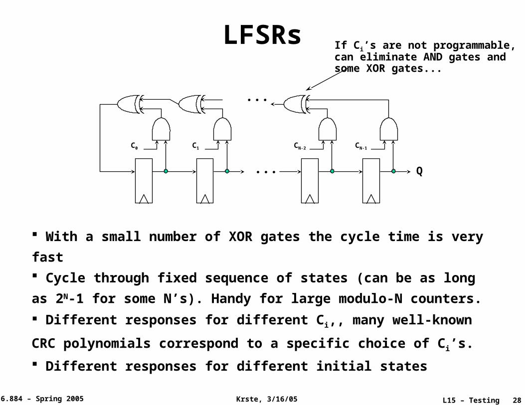
C0 C1 CN-2 CN-1
...
...
Q
If Ci’s are not programmable,can eliminate AND gates andsome XOR gates...
LFSRs
With a small number of XOR gates the cycle time is very
fast Cycle through fixed sequence of states (can be as long as
2N-1 for some N’s). Handy for large modulo-N counters.
Different responses for different Ci,, many well-known CRC
polynomials correspond to a specific choice of Ci’s.
Different responses for different initial states
L15 – Testing 296.884 – Spring 2005 Krste, 3/16/05
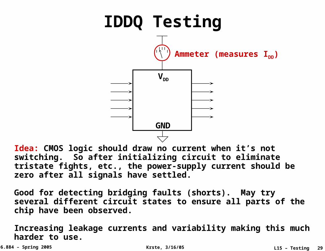
VDD
GND
Ammeter (measures IDD)
Idea: CMOS logic should draw no current when it’s not switching. So after initializing circuit to eliminate tristate fights, etc., the power-supply current should be zero after all signals have settled.
Good for detecting bridging faults (shorts). May try several different circuit states to ensure all parts of the chip have been observed.
Increasing leakage currents and variability making this much harder to use.
IDDQ Testing