L01 Overview CIM 2017 - MITweb.mit.edu/6.101/www/s2017/handouts/L01_4.pdf · CIM Mark Yang LA...
17
Welcome to 6.101! • Introductions, course mechanics • Course overview • Practical issues • Oscilloscope • Circuit review 6.101 Spring 2017 Lecture 1 1 Handouts • Lab kit signout • Lab kit instructions and caution • Lab Hours staffing preference • Student survey form • Reading assignment course outline 6.101 Spring 2017 2 Lecture 1 Other material on course website mit.edu/6.101 Introductions 6.101 Spring 2017 Lecture 1 3 Gim Hom Lecturer Yanni Coroneos TA Jimmy Mawdsley LA Dave Custer CIM Mark Yang LA Farita Tasnim LA Jason Yang LA 6.101 Spring 2017 Lecture 1 4 6.101 Course Website mit.edu/6.101 announcements Online copies of all handouts Staffed lab hours Grades Project presentation & reports submission Technical information Piazza
Transcript of L01 Overview CIM 2017 - MITweb.mit.edu/6.101/www/s2017/handouts/L01_4.pdf · CIM Mark Yang LA...
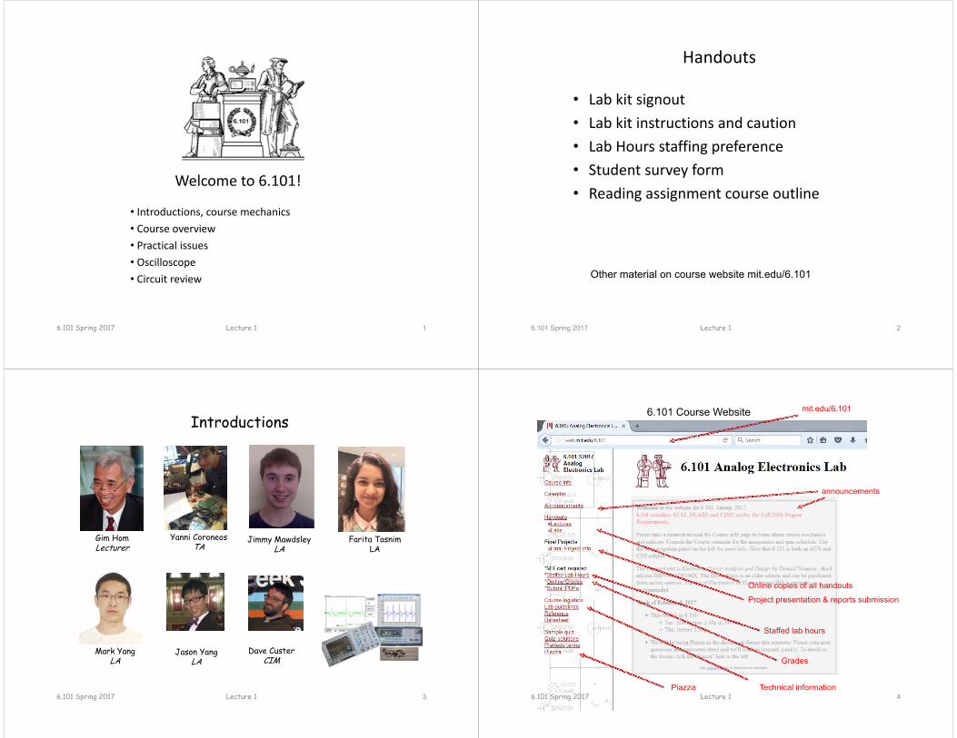
Welcome to 6.101!
• Introductions, course mechanics• Course overview• Practical issues• Oscilloscope• Circuit review
6.101 Spring 2017 Lecture 1 1
Handouts
• Lab kit signout• Lab kit instructions and caution• Lab Hours staffing preference• Student survey form• Reading assignment course outline
6.101 Spring 2017 2Lecture 1
Other material on course website mit.edu/6.101
Introductions
6.101 Spring 2017 Lecture 1 3
Gim HomLecturer
Yanni CoroneosTA
Jimmy MawdsleyLA
Dave CusterCIM
Mark YangLA
Farita TasnimLA
Jason YangLA
6.101 Spring 2017 Lecture 1 4
6.101 Course Website mit.edu/6.101
announcements
Online copies of all handouts
Staffed lab hours
Grades
Project presentation & reports submission
Technical informationPiazza
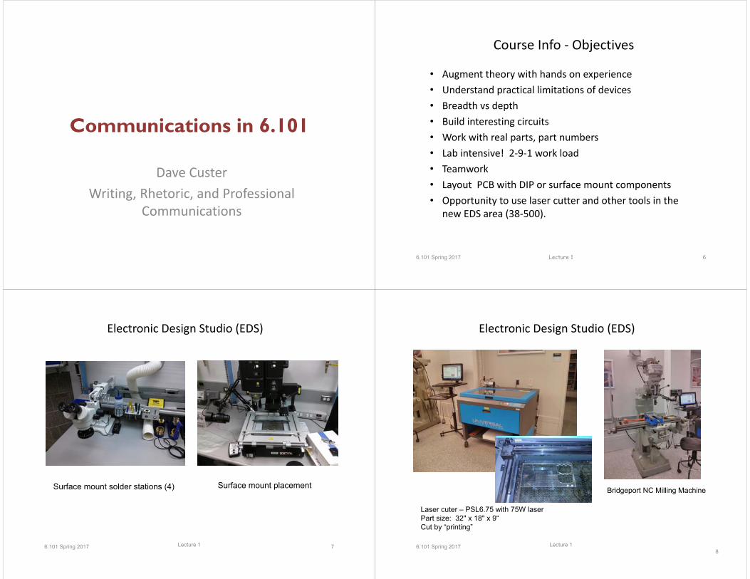
Communications in 6.101
Dave CusterWriting, Rhetoric, and Professional
Communications
Course Info ‐ Objectives
• Augment theory with hands on experience• Understand practical limitations of devices• Breadth vs depth• Build interesting circuits• Work with real parts, part numbers• Lab intensive! 2‐9‐1 work load• Teamwork• Layout PCB with DIP or surface mount components• Opportunity to use laser cutter and other tools in the
new EDS area (38‐500).
6.101 Spring 2017 6Lecture 1
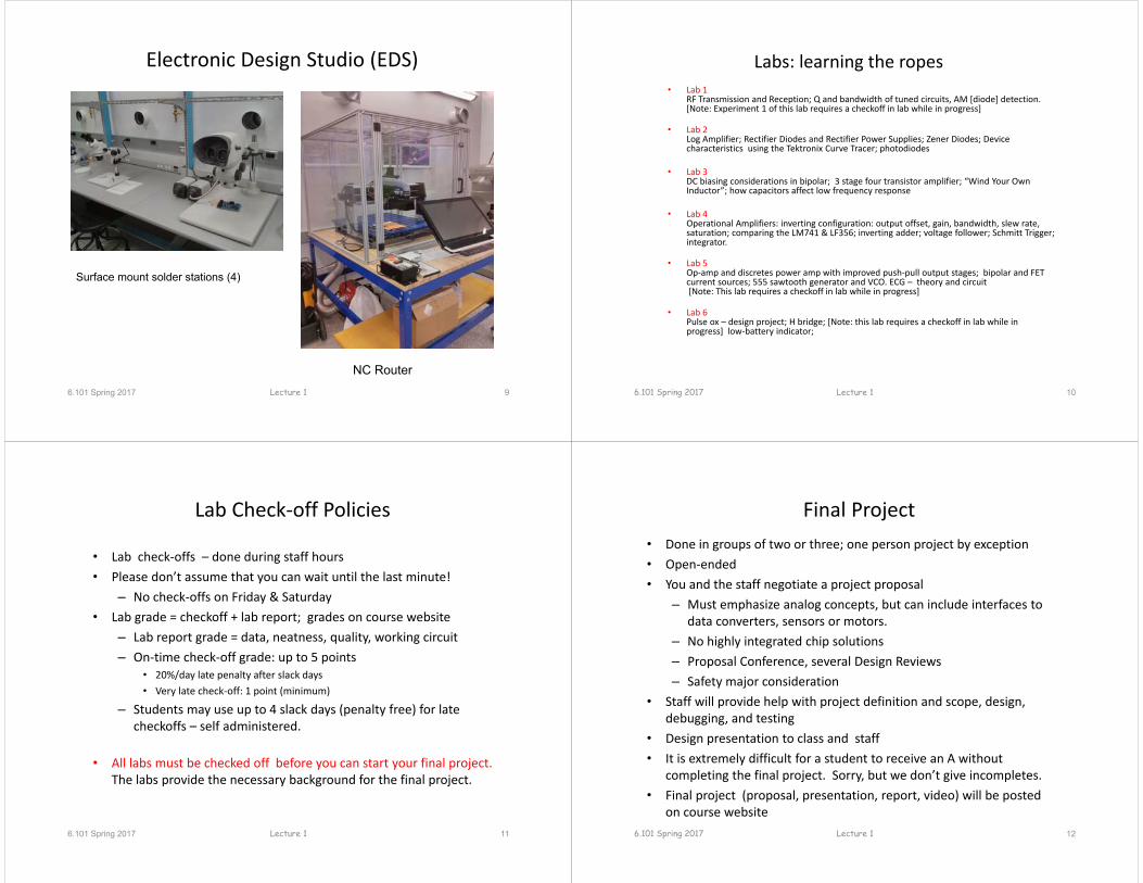
Electronic Design Studio (EDS)
7
Surface mount solder stations (4) Surface mount placement
Lecture 16.101 Spring 2017
Electronic Design Studio (EDS)
8
Laser cuter – PSL6.75 with 75W laserPart size: 32" x 18" x 9“Cut by “printing”
Bridgeport NC Milling Machine
Lecture 16.101 Spring 2017
Electronic Design Studio (EDS)
9Lecture 1
Surface mount solder stations (4)
NC Router
6.101 Spring 2017
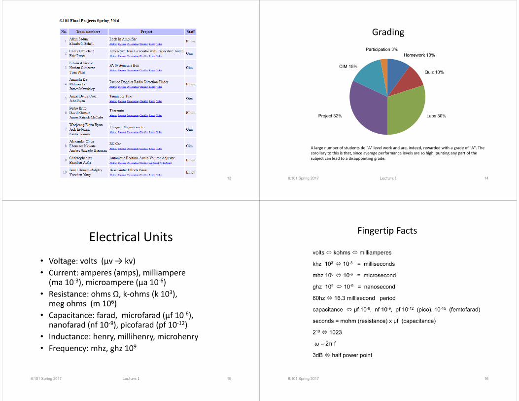
Labs: learning the ropes• Lab 1
RF Transmission and Reception; Q and bandwidth of tuned circuits, AM [diode] detection. [Note: Experiment 1 of this lab requires a checkoff in lab while in progress]
• Lab 2Log Amplifier; Rectifier Diodes and Rectifier Power Supplies; Zener Diodes; Device characteristics using the Tektronix Curve Tracer; photodiodes
• Lab 3 DC biasing considerations in bipolar; 3 stage four transistor amplifier; “Wind Your Own Inductor”; how capacitors affect low frequency response
• Lab 4Operational Amplifiers: inverting configuration: output offset, gain, bandwidth, slew rate, saturation; comparing the LM741 & LF356; inverting adder; voltage follower; Schmitt Trigger; integrator.
• Lab 5Op‐amp and discretes power amp with improved push‐pull output stages; bipolar and FET current sources; 555 sawtooth generator and VCO. ECG – theory and circuit[Note: This lab requires a checkoff in lab while in progress]
• Lab 6Pulse ox – design project; H bridge; [Note: this lab requires a checkoff in lab while in progress] low‐battery indicator;
6.101 Spring 2017 Lecture 1 10
Lab Check‐off Policies
• Lab check‐offs – done during staff hours • Please don’t assume that you can wait until the last minute!
– No check‐offs on Friday & Saturday• Lab grade = checkoff + lab report; grades on course website
– Lab report grade = data, neatness, quality, working circuit– On‐time check‐off grade: up to 5 points
• 20%/day late penalty after slack days• Very late check‐off: 1 point (minimum)
– Students may use up to 4 slack days (penalty free) for late checkoffs – self administered.
• All labs must be checked off before you can start your final project. The labs provide the necessary background for the final project.
6.101 Spring 2017 11Lecture 1
Final Project• Done in groups of two or three; one person project by exception• Open‐ended• You and the staff negotiate a project proposal
– Must emphasize analog concepts, but can include interfaces to data converters, sensors or motors.
– No highly integrated chip solutions– Proposal Conference, several Design Reviews– Safety major consideration
• Staff will provide help with project definition and scope, design, debugging, and testing
• Design presentation to class and staff• It is extremely difficult for a student to receive an A without
completing the final project. Sorry, but we don’t give incompletes.• Final project (proposal, presentation, report, video) will be posted
on course website6.101 Spring 2017 Lecture 1 12
Project Listing ‐ 2014
13
Grading
6.101 Spring 2017 14
A large number of students do "A" level work and are, indeed, rewarded with a grade of "A". The corollary to this is that, since average performance levels are so high, punting any part of the subject can lead to a disappointing grade.
Homework 10%
Quiz 10%
Labs 30%Project 32%
CIM 15%
Participation 3%
Lecture 1
6.101 Spring 2017 15
Electrical Units
• Voltage: volts (μv → kv) • Current: amperes (amps), milliampere (ma 10‐3), microampere (µa 10‐6)
• Resistance: ohms Ω, k‐ohms (k 103), meg ohms (m 106)
• Capacitance: farad, microfarad (µf 10‐6), nanofarad (nf 10‐9), picofarad (pf 10‐12)
• Inductance: henry, millihenry, microhenry• Frequency: mhz, ghz 109
Lecture 1
Fingertip Facts
6.101 Spring 2017 16
volts kohms milliamperes
khz 103 10-3 = milliseconds
60hz 16.3 millisecond period
210 1023
capacitance µf 10-6, nf 10-9, pf 10-12 (pico), 10-15 (femtofarad)
mhz 106 10-6 = microsecond
ghz 109 10-9 = nanosecond
ω = 2π f
3dB half power point
seconds = mohm (resistance) x µf (capacitance)
6.101 Spring 2017 17
Common Acronyms
• BJT – Bipolar Junction Transistor
• MOSFET – Metal Oxide Field Effect Transistor
• PCB – Printed Circuit Board• DIP – dual inline package• SMD, SMT Surface mount
device/technology• cap – capacitor• pot – potentiometer
• AM – amplitude modulation• FM – frequency modulation• RF – radio frequency• IF – intermediate frequency.• dikes – diagonal pliers• 1Nxxx diodes• 2Nxxxx transistors
Lecture 1 6.101 Spring 2017 18
ground resistor, variable
capacitor speaker fuse
npn, pnp mosfetsdiode zener diode
EE Symbols
Inductor transformer
spst spdt dpdtswitches
Lecture 1
6.101 Spring 2017 19
Resistors• V = IR• Resistor parameters: resistance,
tolerance and power rating.• Variable resistors: pots• Resistors are color coded• Standard Values (10%)
10 12 15 18 22 27 33 39 47 56 68 82• Common tolerance: ±5%, ±2%, ±1%• Series/parallel combination• Why is high voltage used in power lines?
i
+
-v
Lecture 1
Nominal Values – Tolerance Ranges
6.101 Spring 2017 20
Series Parallel Combination
6.101 Spring 2017 21
VRR
RV
RRR
R
serieseq
212
...21
2
...2
11
11
RR
R paralleleq
Lecture 1
+VR2-
6.101 Spring 2017 22
Resistor Color Code
red green brown gold2 5 0 Ω 5%
Lecture 1
6.101 Spring 2017 23
2%, 1% Resistor Codes
Lecture 1 6.101 Spring 2017 24
Resistors
Lecture 1
6.101 Spring 2017 25
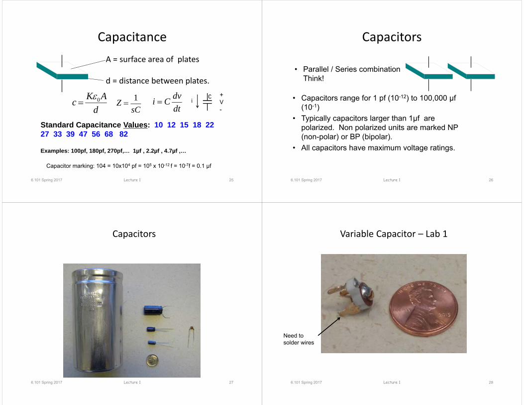
Capacitance
dtdvCi
A = surface area of plates
d = distance between plates.
Capacitor marking: 104 = 10x104 pf = 105 x 10-12 f = 10-7f = 0.1 µf
Standard Capacitance Values: 10 12 15 18 22 27 33 39 47 56 68 82
Examples: 100pf, 180pf, 270pf,… 1µf , 2.2µf , 4.7µf ,…
dAKc 0
+V-
i
Lecture 1
Z 1sC
6.101 Spring 2017 26
Capacitors
• Parallel / Series combinationThink!
• Capacitors range for 1 pf (10-12) to 100,000 µf (10-1)
• Typically capacitors larger than 1µf are polarized. Non polarized units are marked NP (non-polar) or BP (bipolar).
• All capacitors have maximum voltage ratings.
Lecture 1
6.101 Spring 2017 27
Capacitors
Lecture 1 6.101 Spring 2017 28
Variable Capacitor – Lab 1
Lecture 1
Need to solder wires
6.101 Spring 2017 29
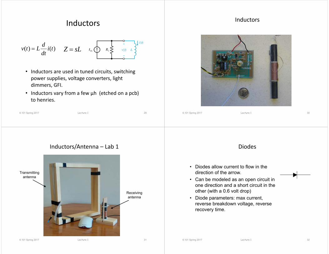
Inductors
• Inductors are used in tuned circuits, switching power supplies, voltage converters, light dimmers, GFI.
• Inductors vary from a few µh (etched on a pcb) to henries.
)()( tidtdLtv
Lecture 1
Z sL
6.101 Spring 2017 30
Inductors
Lecture 1
6.101 Spring 2017 31
Inductors/Antenna – Lab 1
Lecture 1
Transmittingantenna
Receivingantenna
6.101 Spring 2017 32
Diodes
• Diodes allow current to flow in the direction of the arrow.
• Can be modeled as an open circuit in one direction and a short circuit in the other (with a 0.6 volt drop)
• Diode parameters: max current, reverse breakdown voltage, reverse recovery time.
Lecture 1
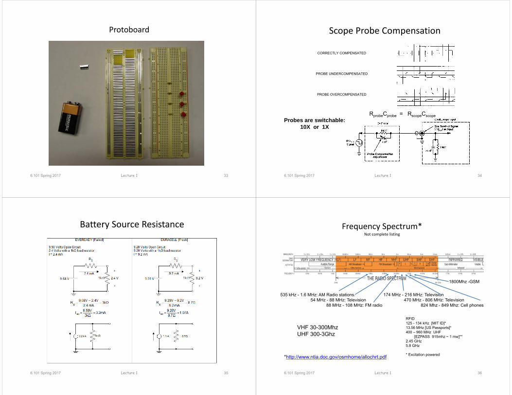
Protoboard
6.101 Spring 2017 33Lecture 1
Scope Probe Compensation
6.101 Spring 2017 34
CORRECTLY COMPENSATED
PROBE UNDERCOMPENSATED
PROBE OVERCOMPENSATED
Lecture 1
RprobeCprobe = RscopeCscopeProbes are switchable:
10X or 1X
Battery Source Resistance
6.101 Spring 2017 35Lecture 1
Frequency Spectrum*Not complete listing
6.101 Spring 2017 36
*http://www.ntia.doc.gov/osmhome/allochrt.pdf
535 kHz - 1.6 MHz: AM Radio stations.54 MHz - 88 MHz: Television
88 MHz - 108 MHz: FM radio
RFID125 - 134 kHz [MIT ID]*13.56 MHz [US Passports]*400 – 960 MHz UHF
[EZPASS 915mhz ~ 1 mw]**2.45 GHz 5.8 GHz
* Excitation powered
VHF 30-300MhzUHF 300-3Ghz
174 MHz - 216 MHz: Television470 MHz - 806 MHz: Television
824 Mhz - 849 Mhz: Cell phones
1800Mhz -GSM
Lecture 1
37
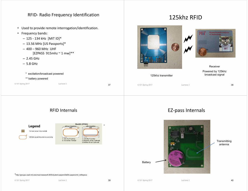
RFID‐ Radio Frequency Identification
• Used to provide remote interrogation/identification.• Frequency bands:
– 125 ‐ 134 kHz [MIT ID]*– 13.56 MHz [US Passports]*– 400 – 960 MHz UHF
[EZPASS 915mhz ~ 1 mw]**– 2.45 GHz – 5.8 GHz
* excitation/broadcast powered
** battery powered
6.101 Spring 2017 Lecture 1 38
125khz RFID
125khz transmitter
Receiver
Powered by 125khz broadcast signal
6.101 Spring 2017 Lecture 1
39
RFID Internals
*
*http://groups.csail.mit.edu/mac/classes/6.805/student-papers/fall04-papers/mit_id/#specs
6.101 Spring 2017 Lecture 1
EZ‐pass Internals
40
Battery
Transmittingantenna
6.101 Spring 2017 Lecture 1
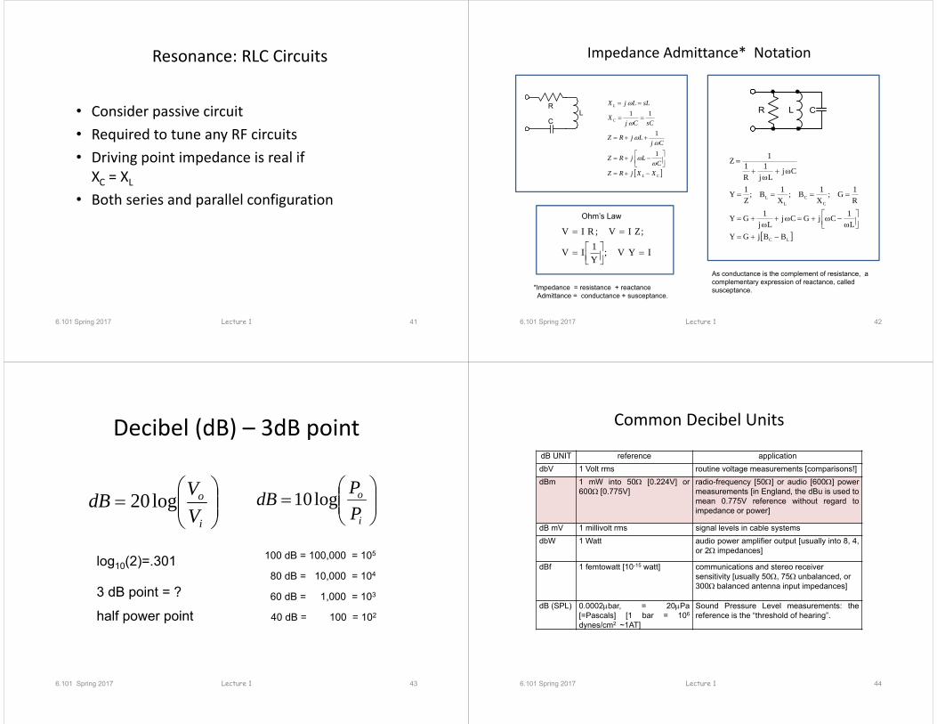
Resonance: RLC Circuits
• Consider passive circuit• Required to tune any RF circuits• Driving point impedance is real ifXC = XL
• Both series and parallel configuration
6.101 Spring 2017 41Lecture 1
Impedance Admittance* Notation
6.101 Spring 2017 42
CL
C
L
XXjRZC
LjRZ
CjLjRZ
sCCjX
sLLjX
1
1
11C
RL
LC
CC
LL
BBjGYL
1CjGCjLj
1GY
R1G;
X1B;
X1B;
Z1Y
CjLj
1R1
1Z
C R L
IYV;Y1IV
;ZIV;RIV
Ohm’s Law
Lecture 1
As conductance is the complement of resistance, a complementary expression of reactance, called susceptance.*Impedance = resistance + reactance
Admittance = conductance + susceptance.
Decibel (dB) – 3dB point
i
o
VVdB log20
i
o
PPdB log10
6.101 Spring 2017 43
3 dB point = ?
log10(2)=.301
Lecture 1
100 dB = 100,000 = 105
80 dB = 10,000 = 104
60 dB = 1,000 = 103
40 dB = 100 = 102half power point
Common Decibel Units
6.101 Spring 2017 44
dB UNIT reference applicationdbV 1 Volt rms routine voltage measurements [comparisons!]dBm 1 mW into 50 [0.224V] or
600 [0.775V]radio-frequency [50] or audio [600] powermeasurements [in England, the dBu is used tomean 0.775V reference without regard toimpedance or power]
dB mV 1 millivolt rms signal levels in cable systemsdbW 1 Watt audio power amplifier output [usually into 8, 4,
or 2 impedances]
dBf 1 femtowatt [10-15 watt] communications and stereo receiver sensitivity [usually 50, 75unbalanced, or 300balanced antenna input impedances]
dB (SPL) 0.0002bar, = 20Pa[=Pascals] [1 bar = 106
dynes/cm2 ~1AT]
Sound Pressure Level measurements: thereference is the “threshold of hearing”.
Lecture 1
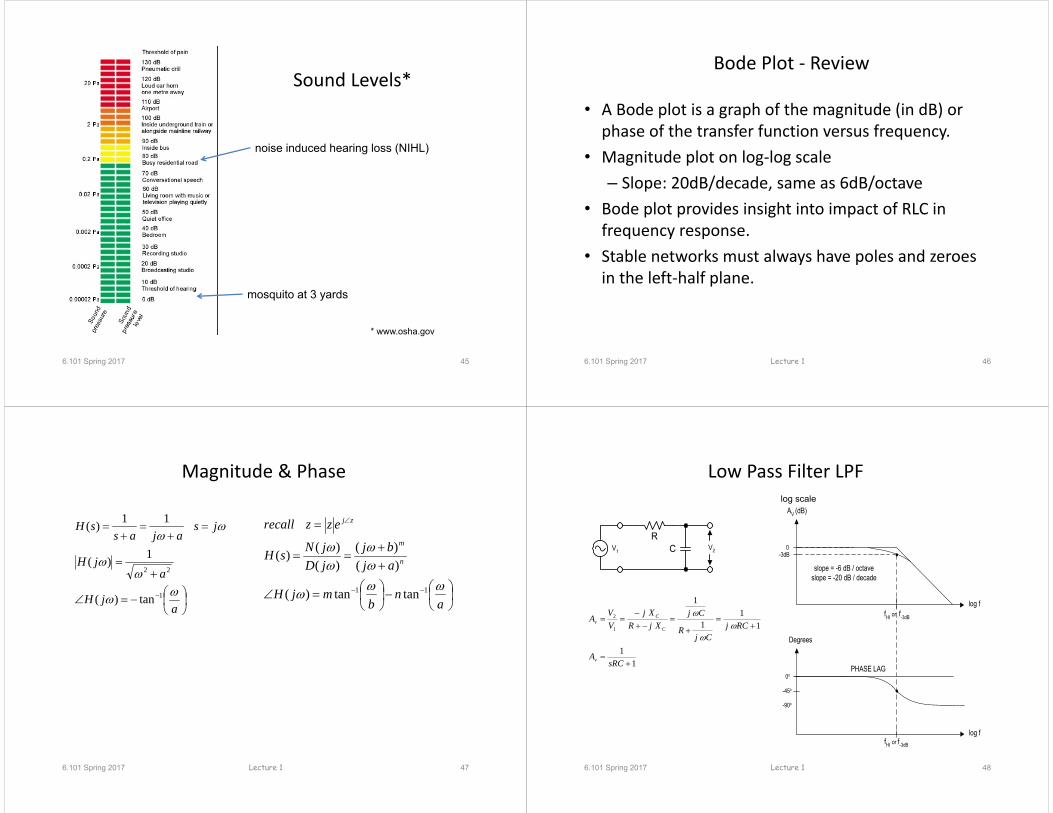
Sound Levels*
6.101 Spring 2017 45
mosquito at 3 yards
* www.osha.gov
noise induced hearing loss (NIHL)
Bode Plot ‐ Review
• A Bode plot is a graph of the magnitude (in dB) or phase of the transfer function versus frequency.
• Magnitude plot on log‐log scale– Slope: 20dB/decade, same as 6dB/octave
• Bode plot provides insight into impact of RLC in frequency response.
• Stable networks must always have poles and zeroes in the left‐half plane.
6.101 Spring 2017 46Lecture 1
Magnitude & Phase
6.101 Spring 2017 47Lecture 1
ajH
ajH
jsajas
sH
1
22
tan)(
1)(
11)(
an
bmjH
ajbj
jDjNsH
ezzrecall
n
m
zj
11 tantan)(
)()(
)()()(
Low Pass Filter LPF
6.101 Spring 2017 48
RV1 V2C
11
11
1
1
1
2
sRCA
RCjCj
R
CjXjR
XjVVA
v
C
Cv
log f
AV (dB)
-3dB
fHI or f-3dB
slope = -6 dB / octaveslope = -20 dB / decade
0
log f
Degrees
-45o
fHI or f-3dB
0o
-90o
PHASE LAG
Lecture 1
log scale
High Pass Filter HPF
6.101 Spring 2017 49
RV1 V2
C
1CRsCRs
1CRjCRj
Cj1R
RVVA
1
2v
log f
AV (dB)
-3dB
fLO or f-3dB
slope = 6 dB / octaveslope = 20 dB / decade
0
log f
Degrees
45o
fLO or f-3dB
90o
0o
-45o
PHASE LEAD
Lecture 1
Transformer – Step Up
6.101 Spring 2017 50
V2 R2V1
1:n
2211 IVIV 22
22
11
2
22
1
21
2
22
1
11
VRVR
RV
RV
RVV
RVV
22
1
21
22
21
21
22
11
12
nRR
soVnRV
nVRVR
nVVbut
Lecture 1
R1 is equivalent resistance of R2 reflected back to primary.
Proper External Grounding forLab 1 IF Transformer
6.101 Spring 2017 51Lecture 1
NC
Can
PC Boardpri sec
Series Resonance
6.101 Spring 2017 52
R L
C
+V-
)1(1C
LjRsC
sLRZ
22 )1(C
LR
VZVI
Lecture 1
Resonance
• I is a maximum at resonance
6.101 Spring 2017 53
22 )1(C
LR
VZVI
CL
1
LCf
fLC
21
21
LjX L
CjXC
1
inductive reactance
capactive reactance
Lecture 1
Resonance (Series RLC) – Key points
6.101 Spring 2017 54
R LC
+V-
)1(1C
LjRsC
sLRZ
• Applies to more complex RLC circuits
• At resonance: power is maximum
• At resonace: phase angle zero, i.e. capacitive reactance = inductive reactance, or impedance is real
Lecture 1
Bandwidth – 3dB Point
6.101 Spring 2017 55
hl
2 f
Bandwith ‐ BW
6.101 Spring 2017 56
• BW (radians) = where are the half power points
• Peak power is at resonance
• Half power points
• Note:
RVP
2
RVI2
22 )1(C
LR
VZVI
22 )1(2wc
wLRR LCLR
LR 1
22
2
1
LCLR
LR 1
22
2
2
212
lh lh ,
Lecture 1
Bandwidth and Q (Series RLC)
6.101 Spring 2017 57
• BW (hertz) =
• Q* (quality factor)
• Higher Q implies more selectivity
LRlh
22
resonant frequencybandwidth
*Agarwal/Lang Foundation of Analog Digital Elect Circuits equation 14.47, p 794
CL
RQ 1
Lecture 1
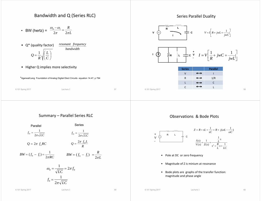
Series Parallel Duality
6.101 Spring 2017 58
I R L C+V-
I
R L
CV
jwLjwC
RVI 11
jwCjwLRIV 1
Series Parallel
V I
R 1/R
L C
C L
Summary – Parallel Series RLC
6.101 Spring 2017 59
RLfQ O2
LCfO 2
1
RCfQ o2
LRffBW lh 2
)( RC
ffBW lh 21)(
LCf
fLC
21
21
0
00
Parallel Series
Lecture 1
LCfO 2
1
Observations & Bode Plots
6.101 Spring 2017 60
R LC
+V-
)1(1C
LjRsC
sLRZ
• Pole at DC or zero frequency
• Magnitude of Z is minium at resonance
• Bode plots are graphs of the transfer function: magnitude and phase angle
2
1( ) 1
1( ) ( )
sI s LRV s Z s s sL LC
Lecture 1
MATLAB Functions bode, freqs
• BODE(SYS,W) uses the vector W of frequencies (in radians/TimeUnit) to evaluate the frequency response
• [MAG,PHASE] = BODE(SYS,W) and [MAG,PHASE,W] = BODE(SYS) return the response magnitudes and phases in degrees (along with the frequency vector W if unspecified).
• SYS is the transfer function expressed as numerator and denominator in the form
• bode(num,denom,range)num=[d e], denom=[a b c], range= desired freqencies in radians
• freqs(num,denom,range) plots frequency response and phase angle
6.101 Spring 2017 61
cbsasesdSYS
2
Lecture 1
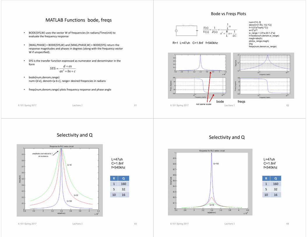
Bode vs Freqs Plots
6.101 Spring 2017 62freqs
R=1 L=47uh C=1.8nf f=540khz
num=[1/L 0]denom=[1 R/L 1/(L*C)]f=1/(2*pi*sqrt(L*C))w=2*pi*fw_range = [.8*w:20:1.2*w]h=bode(num,denom,w_range)magh=abs(h)plot(w_range,magh)shgfreqs(num,denom,w_range)
bode not same scale
2
1( ) 1
1( ) ( )
sI s LRV s Z s s sL LC
Lecture 1
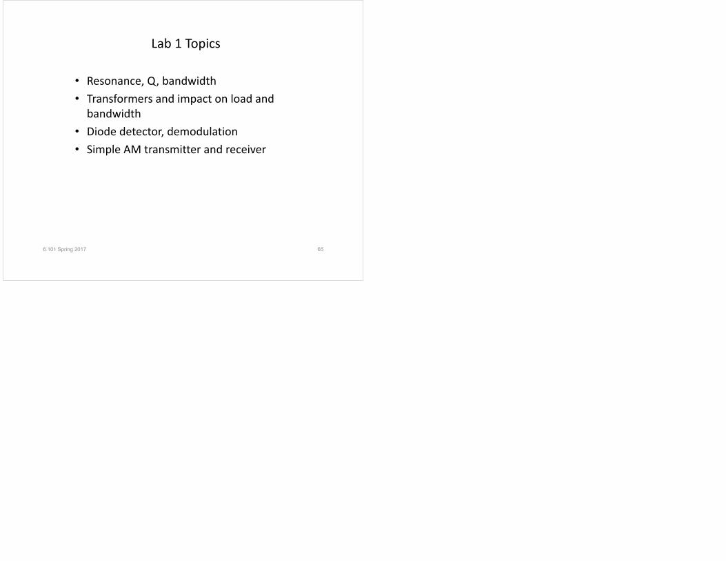
Selectivity and Q
6.101 Spring 2017 63
L=47uh C=1.8nf f=540khz
R Q
1 160
5 32
10 16
Lecture 1
Selectivity and Q
6.101 Spring 2017 64
L=47uh C=1.8nf f=540khz
R Q
1 160
5 32
10 16
Lecture 1
Lab 1 Topics
• Resonance, Q, bandwidth• Transformers and impact on load and bandwidth
• Diode detector, demodulation• Simple AM transmitter and receiver
6.101 Spring 2017 65


![ETSI ISG CIM · [JSON-LD] 20170608 Introduction to ISG CIM CIM-002-UC CIM -003 GAP CIM-004-APIprelim CIM-005-DPP CIM-001-AB ) CIM-006-MOD0. Timeline in ToR 02/2017 First General Meeting](https://static.fdocuments.net/doc/165x107/6002860fd1e0f63f360db5f2/etsi-isg-cim-json-ld-20170608-introduction-to-isg-cim-cim-002-uc-cim-003-gap.jpg)