Key Advantages of Arria V Devices -...
33
Arria V Device Overview 2013.01.11 AV-51001 Subscribe Feedback The Arria ® V device family consists of the most comprehensive offerings of mid-range FPGAs ranging from the lowest power for 6 gigabits per second (Gbps) and 10 Gbps applications, to the highest mid-range FPGA bandwidth 12.5 Gbps transceivers. The Arria V devices are ideal for power-sensitive wireless infrastructure equipment, 20G/40G bridging, switching, and packet processing applications, high-definition video processing and image manipulation, and intensive digital signal processing (DSP) applications. Key Advantages of Arria V Devices Table 1: Key Advantages of the Arria V Device Family Supporting Feature Advantage • Built on TSMC's 28 nm process technology and includes an abundance of hard intellectual property (IP) blocks • Power-optimized MultiTrack routing and core architecture • Up to 50% lower power consumption than the previous generation device • Lowest power transceivers of any midrange family Lowest static power in its class • 8-input adaptive logic module (ALM) • Up to 38.38 megabits (Mb) of embedded memory • Variable-precision digital signal processing (DSP) blocks Improved logic integration and differentiation capabilities • Serial data rates up to 12.5 Gbps • Hard memory controllers Increased bandwidth capacity • Tight integration of a dual-core ARM Cortex-A9 MPCore processor, hard IP, and an FPGA in a single Arria V system-on-a-chip (SoC) FPGA • Supports over 128 Gbps peak bandwidth with integrated data coherency between the processor and the FPGA fabric Hard processor system (HPS) with integrated ARM ® Cortex ™ -A9 MPCore processor • Requires as low as four power supplies to operate • Available in thermal composite flip chip ball-grid array (BGA) packaging • Includes innovative features such as Configuration via Protocol (CvP), partial reconfiguration, and design security Lowest system cost ISO 9001:2008 Registered © 2013 Altera Corporation. All rights reserved. ALTERA, ARRIA, CYCLONE, HARDCOPY, MAX, MEGACORE, NIOS, QUARTUS and STRATIX words and logos are trademarks of Altera Corporation and registered in the U.S. Patent and Trademark Office and in other countries. All other words and logos identified as trademarks or service marks are the property of their respective holders as described at www.altera.com/common/legal.html. Altera warrants performance of its semiconductor products to current specifications in accordance with Altera's standard warranty, but reserves the right to make changes to any products and services at any time without notice. Altera assumes no responsibility or liability arising out of the application or use of any information, product, or service described herein except as expressly agreed to in writing by Altera. Altera customers are advised to obtain the latest version of device specifications before relying on any published information and before placing orders for products or services. www.altera.com 101 Innovation Drive, San Jose, CA 95134 Downloaded from Elcodis.com electronic components distributor
Transcript of Key Advantages of Arria V Devices -...

Arria V Device Overview2013.01.11
AV-51001 Subscribe Feedback
The Arria®V device family consists of the most comprehensive offerings of mid-range FPGAs ranging fromthe lowest power for 6 gigabits per second (Gbps) and 10 Gbps applications, to the highest mid-range FPGAbandwidth 12.5 Gbps transceivers.
The Arria V devices are ideal for power-sensitive wireless infrastructure equipment, 20G/40G bridging,switching, and packet processing applications, high-definition video processing and image manipulation,and intensive digital signal processing (DSP) applications.
Key Advantages of Arria V Devices
Table 1: Key Advantages of the Arria V Device Family
Supporting FeatureAdvantage
• Built on TSMC's 28 nm process technology and includes an abundance ofhard intellectual property (IP) blocks
• Power-optimized MultiTrack routing and core architecture• Up to 50% lower power consumption than the previous generation device• Lowest power transceivers of any midrange family
Lowest static power in its class
• 8-input adaptive logic module (ALM)• Up to 38.38 megabits (Mb) of embedded memory• Variable-precision digital signal processing (DSP) blocks
Improved logic integration anddifferentiation capabilities
• Serial data rates up to 12.5 Gbps• Hard memory controllers
Increased bandwidth capacity
• Tight integration of a dual-core ARM Cortex-A9 MPCore processor, hardIP, and an FPGA in a single Arria V system-on-a-chip (SoC) FPGA
• Supports over 128 Gbps peak bandwidth with integrated data coherencybetween the processor and the FPGA fabric
Hard processor system (HPS)with integrated ARM®
Cortex™-A9MPCoreprocessor
• Requires as low as four power supplies to operate• Available in thermal composite flip chip ball-grid array (BGA) packaging• Includes innovative features such as Configuration via Protocol (CvP),
partial reconfiguration, and design security
Lowest system cost
ISO9001:2008Registered
© 2013 Altera Corporation. All rights reserved. ALTERA, ARRIA, CYCLONE, HARDCOPY, MAX, MEGACORE, NIOS, QUARTUS and STRATIX wordsand logos are trademarks of Altera Corporation and registered in the U.S. Patent and Trademark Office and in other countries. All otherwords and logos identified as trademarks or service marks are the property of their respective holders as described atwww.altera.com/common/legal.html. Altera warrants performance of its semiconductor products to current specifications in accordance withAltera's standard warranty, but reserves the right to make changes to any products and services at any time without notice. Altera assumesno responsibility or liability arising out of the application or use of any information, product, or service described herein except as expresslyagreed to in writing by Altera. Altera customers are advised to obtain the latest version of device specifications before relying on any publishedinformation and before placing orders for products or services.
www.altera.com
101 Innovation Drive, San Jose, CA 95134
Downloaded from Elcodis.com electronic components distributor
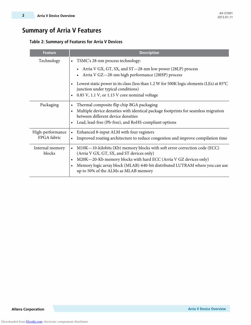
Summary of Arria V Features
Table 2: Summary of Features for Arria V Devices
DescriptionFeature
• TSMC's 28-nm process technology:
• Arria V GX, GT, SX, and ST—28-nm low power (28LP) process• Arria V GZ—28-nm high performance (28HP) process
• Lowest static power in its class (less than 1.2 W for 500K logic elements (LEs) at 85°Cjunction under typical conditions)
• 0.85 V, 1.1 V, or 1.15 V core nominal voltage
Technology
• Thermal composite flip chip BGA packaging• Multiple device densities with identical package footprints for seamless migration
between different device densities• Lead, lead-free (Pb-free), and RoHS-compliant options
Packaging
• Enhanced 8-input ALM with four registers• Improved routing architecture to reduce congestion and improve compilation time
High-performanceFPGA fabric
• M10K—10-kilobits (Kb) memory blocks with soft error correction code (ECC)(Arria V GX, GT, SX, and ST devices only)
• M20K—20-Kb memory blocks with hard ECC (Arria V GZ devices only)• Memory logic array block (MLAB)-640-bit distributed LUTRAM where you can use
up to 50% of the ALMs as MLAB memory
Internal memoryblocks
Arria V Device OverviewAltera Corporation
AV-51001Arria V Device Overview2 2013.01.11
Downloaded from Elcodis.com electronic components distributor
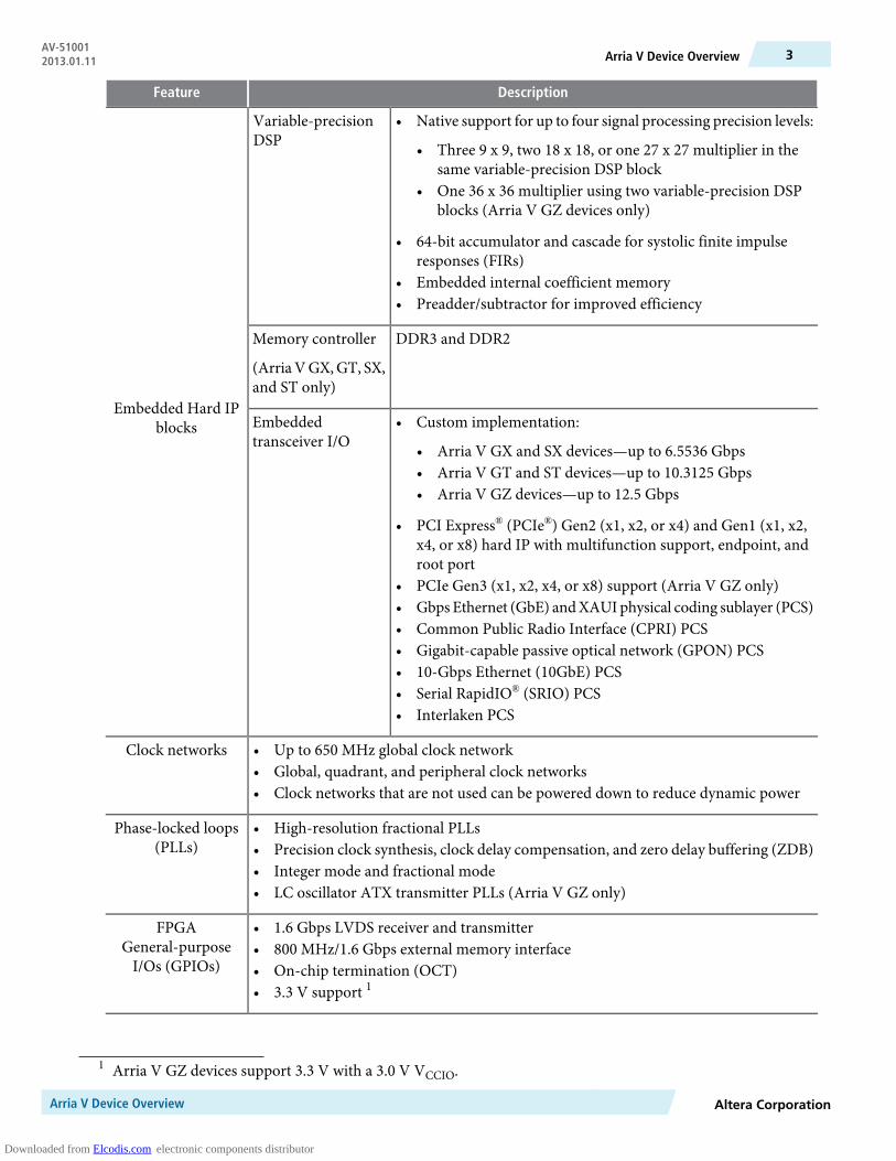
DescriptionFeature
• Native support for up to four signal processing precision levels:
• Three 9 x 9, two 18 x 18, or one 27 x 27 multiplier in thesame variable-precision DSP block
• One 36 x 36 multiplier using two variable-precision DSPblocks (Arria V GZ devices only)
• 64-bit accumulator and cascade for systolic finite impulseresponses (FIRs)
• Embedded internal coefficient memory• Preadder/subtractor for improved efficiency
Variable-precisionDSP
Embedded Hard IPblocks
DDR3 and DDR2Memory controller
(ArriaVGX,GT, SX,and ST only)
• Custom implementation:
• Arria V GX and SX devices—up to 6.5536 Gbps• Arria V GT and ST devices—up to 10.3125 Gbps• Arria V GZ devices—up to 12.5 Gbps
• PCI Express® (PCIe®) Gen2 (x1, x2, or x4) and Gen1 (x1, x2,x4, or x8) hard IP with multifunction support, endpoint, androot port
• PCIe Gen3 (x1, x2, x4, or x8) support (Arria V GZ only)• Gbps Ethernet (GbE) andXAUIphysical coding sublayer (PCS)• Common Public Radio Interface (CPRI) PCS• Gigabit-capable passive optical network (GPON) PCS• 10-Gbps Ethernet (10GbE) PCS• Serial RapidIO® (SRIO) PCS• Interlaken PCS
Embeddedtransceiver I/O
• Up to 650 MHz global clock network• Global, quadrant, and peripheral clock networks• Clock networks that are not used can be powered down to reduce dynamic power
Clock networks
• High-resolution fractional PLLs• Precision clock synthesis, clock delay compensation, and zero delay buffering (ZDB)• Integer mode and fractional mode• LC oscillator ATX transmitter PLLs (Arria V GZ only)
Phase-locked loops(PLLs)
• 1.6 Gbps LVDS receiver and transmitter• 800 MHz/1.6 Gbps external memory interface• On-chip termination (OCT)• 3.3 V support 1
FPGAGeneral-purposeI/Os (GPIOs)
1 Arria V GZ devices support 3.3 V with a 3.0 V VCCIO.
Altera CorporationArria V Device Overview
3Arria V Device OverviewAV-510012013.01.11
Downloaded from Elcodis.com electronic components distributor
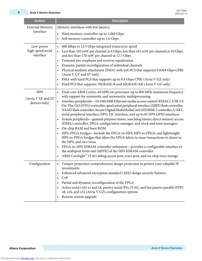
DescriptionFeature
Memory interfaces with low latency:
• Hard memory controller-up to 1.066 Gbps• Soft memory controller-up to 1.6 Gbps
External MemoryInterface
• 600 Mbps to 12.5 Gbps integrated transceiver speed• Less than 105 mW per channel at 6 Gbps, less than 165 mW per channel at 10 Gbps,
and less than 170 mW per channel at 12.5 Gbps• Transmit pre-emphasis and receiver equalization• Dynamic partial reconfiguration of individual channels• Physical medium attachment (PMA) with soft PCS that supports 9.8304 Gbps CPRI
(Arria V GT and ST only)• PMA with hard PCS that supports up to 9.8 Gbps CPRI (Arria V GZ only)• Hard PCS that supports 10GBASE-R and 10GBASE-KR (Arria V GZ only)
Low-powerhigh-speed serial
interface
• Dual-core ARM Cortex-A9 MPCore processor-up to 800 MHz maximum frequencywith support for symmetric and asymmetric multiprocessing
• Interface peripherals—10/100/1000 Ethernet media access control (EMAC), USB 2.0On-The-GO (OTG) controller, quad serial peripheral interface (QSPI) flash controller,NANDflash controller, SecureDigital/MultiMediaCard (SD/MMC) controller,UART,serial peripheral interface (SPI), I2C interface, and up to 85 HPS GPIO interfaces
• System peripherals—general-purpose timers, watchdog timers, directmemory access(DMA) controller, FPGA configuration manager, and clock and reset managers
• On-chip RAM and boot ROM• HPS–FPGA bridges—include the FPGA-to-HPS, HPS-to-FPGA, and lightweight
HPS-to-FPGA bridges that allow the FPGA fabric to issue transactions to slaves inthe HPS, and vice versa
• FPGA-to-HPS SDRAM controller subsystem—provides a configurable interface tothe multiport front end (MPFE) of the HPS SDRAM controller
• ARM CoreSight™ JTAG debug access port, trace port, and on-chip trace storage
HPS
(Arria V SX and STdevices only)
• Tamper protection-comprehensive design protection to protect your valuable IPinvestments
• Enhanced advanced encryption standard (AES) design security features• CvP• Partial and dynamic reconfiguration of the FPGA• Active serial (AS) x1 and x4, passive serial (PS), JTAG, and fast passive parallel (FPP)
x8, x16, and x32 (Arria V GZ) configuration options• Remote system upgrade
Configuration
Arria V Device OverviewAltera Corporation
AV-51001Arria V Device Overview4 2013.01.11
Downloaded from Elcodis.com electronic components distributor
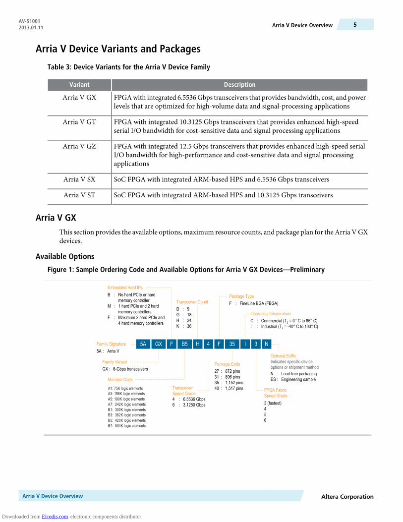
Arria V Device Variants and Packages
Table 3: Device Variants for the Arria V Device Family
DescriptionVariant
FPGAwith integrated 6.5536Gbps transceivers that provides bandwidth, cost, and powerlevels that are optimized for high-volume data and signal-processing applications
Arria V GX
FPGA with integrated 10.3125 Gbps transceivers that provides enhanced high-speedserial I/O bandwidth for cost-sensitive data and signal processing applications
Arria V GT
FPGA with integrated 12.5 Gbps transceivers that provides enhanced high-speed serialI/O bandwidth for high-performance and cost-sensitive data and signal processingapplications
Arria V GZ
SoC FPGA with integrated ARM-based HPS and 6.5536 Gbps transceiversArria V SX
SoC FPGA with integrated ARM-based HPS and 10.3125 Gbps transceiversArria V ST
Arria V GXThis section provides the available options, maximum resource counts, and package plan for the Arria V GXdevices.
Available Options
Figure 1: Sample Ordering Code and Available Options for Arria V GX Devices—Preliminary
Family Signature
Embedded Hard IPs
Transceiver Count
TransceiverSpeed Grade
Package Type
Package Code
Operating Temperature
FPGA FabricSpeed Grade
Optional SuffixIndicates specific deviceoptions or shipment methodGX : 6-Gbps transceivers
B : No hard PCIe or hardmemory controller
M : 1 hard PCIe and 2 hardmemory controllers
F : Maximum 2 hard PCIe and4 hard memory controllers
5A : Arria V
A1: 75K logic elementsA3: 156K logic elementsA5: 190K logic elementsA7: 242K logic elementsB1: 300K logic elementsB3: 362K logic elementsB5: 420K logic elementsB7: 504K logic elements
D : 9G : 18H : 24K : 36
4 : 6.5536 Gbps6 : 3.1250 Gbps
F : FineLine BGA (FBGA)
27 : 672 pins31 : 896 pins35 : 1,152 pins40 : 1,517 pins
C : Commercial (TJ = 0° C to 85° C)I : Industrial (TJ = -40° C to 100° C)
3 (fastest)456
N : Lead-free packagingES : Engineering sample
5A GX F B5 H 4 F 35 I 3 N
Member Code
Family Variant
Altera CorporationArria V Device Overview
5Arria V Device OverviewAV-510012013.01.11
Downloaded from Elcodis.com electronic components distributor
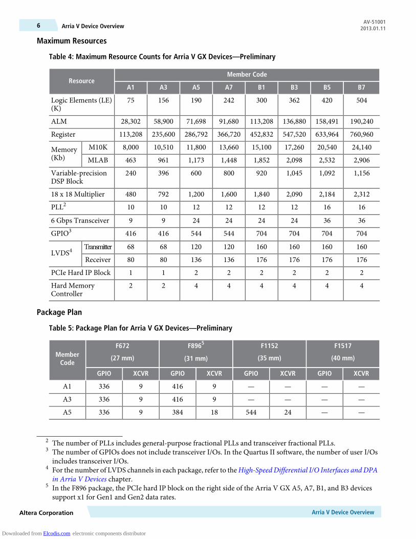
Maximum Resources
Table 4: Maximum Resource Counts for Arria V GX Devices—Preliminary
Member CodeResource
B7B5B3B1A7A5A3A1
50442036230024219015675Logic Elements (LE)(K)
190,240158,491136,880113,20891,68071,69858,90028,302ALM
760,960633,964547,520452,832366,720286,792235,600113,208Register
24,14020,54017,26015,10013,66011,80010,5108,000M10KMemory(Kb) 2,9062,5322,0981,8521,4481,173961463MLAB
1,1561,0921,045920800600396240Variable-precisionDSP Block
2,3122,1842,0901,8401,6001,20079248018 x 18 Multiplier
1616121212121010PLL2
363624242424996 Gbps Transceiver
704704704704544544416416GPIO3
1601601601601201206868TransmitterLVDS4
1761761761761361368080Receiver
22222211PCIe Hard IP Block
44444422Hard MemoryController
Package Plan
Table 5: Package Plan for Arria V GX Devices—Preliminary
F1517
(40 mm)
F1152
(35 mm)
F8965
(31 mm)
F672
(27 mm)MemberCode
XCVRGPIOXCVRGPIOXCVRGPIOXCVRGPIO
————94169336A1
————94169336A3
——24544183849336A5
2 The number of PLLs includes general-purpose fractional PLLs and transceiver fractional PLLs.3 The number of GPIOs does not include transceiver I/Os. In the Quartus II software, the number of user I/Os
includes transceiver I/Os.4 For the number of LVDS channels in each package, refer to theHigh-Speed Differential I/O Interfaces and DPA
in Arria V Devices chapter.5 In the F896 package, the PCIe hard IP block on the right side of the Arria V GX A5, A7, B1, and B3 devices
support x1 for Gen1 and Gen2 data rates.
Arria V Device OverviewAltera Corporation
AV-51001Arria V Device Overview6 2013.01.11
Downloaded from Elcodis.com electronic components distributor
F1517
(40 mm)
F1152
(35 mm)
F8965
(31 mm)
F672
(27 mm)MemberCode
XCVRGPIOXCVRGPIOXCVRGPIOXCVRGPIO
——24544183849336A7
247042454418384——B1
247042454418384——B3
3670424544————B5
3670424544————B7
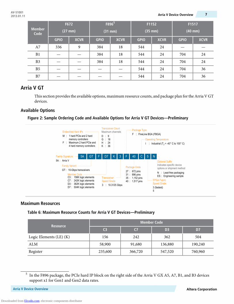
Arria V GTThis section provides the available options, maximum resource counts, and package plan for the Arria V GTdevices.
Available Options
Figure 2: Sample Ordering Code and Available Options for Arria V GT Devices—Preliminary
Family Signature
Embedded Hard IPsTransceiver CountMaximum channels
TransceiverSpeed Grade
Package Type
Package Code
Operating Temperature
FPGA FabricSpeed Grade
Optional SuffixIndicates specific deviceoptions or shipment methodGT : 10-Gbps transceivers
M : 1 hard PCIe and 2 hardmemory controllers
F : Maximum 2 hard PCIe and4 hard memory controllers
5A : Arria V
C3 : 156K logic elementsC7 : 242K logic elementsD3 : 362K logic elementsD7 : 504K logic elements
D : 9G : 18H : 24K : 36
3 : 10.3125 Gbps
F : FineLine BGA (FBGA)
27 : 672 pins31 : 896 pins35 : 1,152 pins40 : 1,517 pins
3 (fastest)5
N : Lead-free packagingES : Engineering sample
5A GT F D7 K 3 F 40 C 5 N
Member Code
Family Variant
I : Industrial (TJ = -40° C to 100° C)
Maximum Resources
Table 6: Maximum Resource Counts for Arria V GT Devices—Preliminary
Member CodeResource
D7D3C7C3
504362242156Logic Elements (LE) (K)
190,240136,88091,68058,900ALM
760,960547,520366,720235,600Register
5 In the F896 package, the PCIe hard IP block on the right side of the Arria V GX A5, A7, B1, and B3 devicessupport x1 for Gen1 and Gen2 data rates.
Altera CorporationArria V Device Overview
7Arria V Device OverviewAV-510012013.01.11
Downloaded from Elcodis.com electronic components distributor
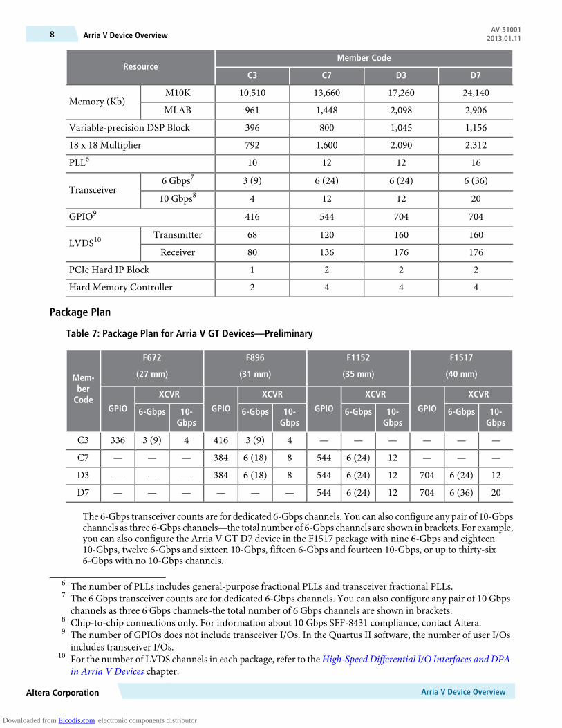
Member CodeResource
D7D3C7C3
24,14017,26013,66010,510M10KMemory (Kb)
2,9062,0981,448961MLAB
1,1561,045800396Variable-precision DSP Block
2,3122,0901,60079218 x 18 Multiplier
16121210PLL6
6 (36)6 (24)6 (24)3 (9)6 Gbps7Transceiver
201212410 Gbps8
704704544416GPIO9
16016012068TransmitterLVDS10
17617613680Receiver
2221PCIe Hard IP Block
4442Hard Memory Controller
Package Plan
Table 7: Package Plan for Arria V GT Devices—Preliminary
F1517
(40 mm)
F1152
(35 mm)
F896
(31 mm)
F672
(27 mm)Mem-ber
CodeXCVR
GPIO
XCVR
GPIO
XCVR
GPIO
XCVR
GPIO 10-Gbps
6-Gbps10-Gbps
6-Gbps10-Gbps
6-Gbps10-Gbps
6-Gbps
——————43 (9)41643 (9)336C3
———126 (24)54486 (18)384———C7
126 (24)704126 (24)54486 (18)384———D3
206 (36)704126 (24)544——————D7
The 6-Gbps transceiver counts are for dedicated 6-Gbps channels. You can also configure any pair of 10-Gbpschannels as three 6-Gbps channels—the total number of 6-Gbps channels are shown in brackets. For example,you can also configure the Arria V GT D7 device in the F1517 package with nine 6-Gbps and eighteen10-Gbps, twelve 6-Gbps and sixteen 10-Gbps, fifteen 6-Gbps and fourteen 10-Gbps, or up to thirty-six6-Gbps with no 10-Gbps channels.
6 The number of PLLs includes general-purpose fractional PLLs and transceiver fractional PLLs.7 The 6 Gbps transceiver counts are for dedicated 6-Gbps channels. You can also configure any pair of 10 Gbps
channels as three 6 Gbps channels-the total number of 6 Gbps channels are shown in brackets.8 Chip-to-chip connections only. For information about 10 Gbps SFF-8431 compliance, contact Altera.9 The number of GPIOs does not include transceiver I/Os. In the Quartus II software, the number of user I/Os
includes transceiver I/Os.10 For the number of LVDS channels in each package, refer to theHigh-Speed Differential I/O Interfaces and DPA
in Arria V Devices chapter.
Arria V Device OverviewAltera Corporation
AV-51001Arria V Device Overview8 2013.01.11
Downloaded from Elcodis.com electronic components distributor
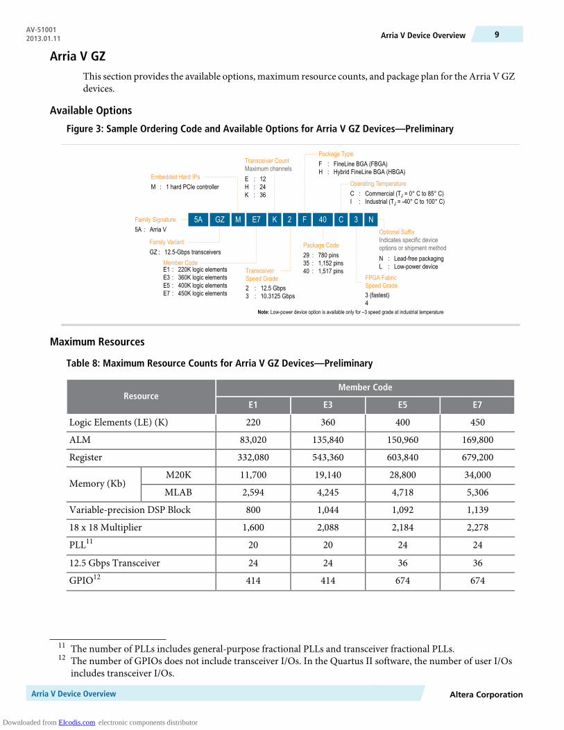
Arria V GZThis section provides the available options, maximum resource counts, and package plan for the Arria V GZdevices.
Available Options
Figure 3: Sample Ordering Code and Available Options for Arria V GZ Devices—Preliminary
Family Signature
Embedded Hard IPs
Transceiver CountMaximum channels
TransceiverSpeed Grade
Package Type
Package Code
Operating Temperature
FPGA FabricSpeed Grade
Optional SuffixIndicates specific deviceoptions or shipment methodGZ : 12.5-Gbps transceivers
M : 1 hard PCIe controller
5A : Arria V
E1 : 220K logic elementsE3 : 360K logic elementsE5 : 400K logic elementsE7 : 450K logic elements
E : 12H : 24K : 36
2 : 12.5 Gbps3 : 10.3125 Gbps
F : FineLine BGA (FBGA)H : Hybrid FineLine BGA (HBGA)
29 : 780 pins35 : 1,152 pins40 : 1,517 pins
3 (fastest)4
N : Lead-free packagingL : Low-power device
5A GZ M E7 K 2 F 40 C 3 N
Member Code
Family Variant
C : Commercial (TJ = 0° C to 85° C)I : Industrial (TJ = -40° C to 100° C)
Note: Low-power device option is available only for –3 speed grade at industrial temperature
Maximum Resources
Table 8: Maximum Resource Counts for Arria V GZ Devices—Preliminary
Member CodeResource
E7E5E3E1
450400360220Logic Elements (LE) (K)
169,800150,960135,84083,020ALM
679,200603,840543,360332,080Register
34,00028,80019,14011,700M20KMemory (Kb)
5,3064,7184,2452,594MLAB
1,1391,0921,044800Variable-precision DSP Block
2,2782,1842,0881,60018 x 18 Multiplier
24242020PLL11
3636242412.5 Gbps Transceiver
674674414414GPIO12
11 The number of PLLs includes general-purpose fractional PLLs and transceiver fractional PLLs.12 The number of GPIOs does not include transceiver I/Os. In the Quartus II software, the number of user I/Os
includes transceiver I/Os.
Altera CorporationArria V Device Overview
9Arria V Device OverviewAV-510012013.01.11
Downloaded from Elcodis.com electronic components distributor

Member CodeResource
E7E5E3E1
1661669999TransmitterLVDS13
168168108108Receiver
1111PCIe Hard IP Block
Package Plan
Table 9: Package Plan for Arria V GZ Devices—Preliminary
F1517
(40 mm)
F1152
(35 mm)
H780
(29 mm)Member Code
XCVRGPIOXCVRGPIOXCVRGPIO
——2441412342E1
——2441412342E3
3667424534——E5
3667424534——E7
Arria V SXThis section provides the available options, maximum resource counts, and package plan for the Arria V SXdevices.
Available Options
Figure 4: Sample Ordering Code and Available Options for Arria V SX Devices—Preliminary
Family Signature
Embedded Hard IPsTransceiver Count
TransceiverSpeed Grade
Package Type
Package Code
Operating Temperature
FPGA FabricSpeed Grade
Optional SuffixIndicates specific deviceoptions or shipment methodSX : SoC FPGA with 6-Gbps transceivers
F : Maximum 2 hard PCIecontrollers and 3 hardmemory controllers
5A : Arria V
B3 : 350K logic elementsB5 : 462K logic elements
E : 12G : 18H : 30
4 : 6.5336 Gbps6 : 3.1250 Gbps
F : FineLine BGA (FBGA)
31 : 896 pins35 : 1,152 pins40 : 1,517 pins
C : Commercial (TJ = 0° C to 85° C)I : Industrial (TJ = -40° C to 100° C)
4 (fastest)56
N : Lead-free packagingES : Engineering sample
5A SX F B5 H 4 F 40 C 4 N
Member Code
Family Variant
13 For the number of LVDS channels in each package, refer to theHigh-Speed Differential I/O Interfaces and DPAin Arria V Devices chapter.
Arria V Device OverviewAltera Corporation
AV-51001Arria V Device Overview10 2013.01.11
Downloaded from Elcodis.com electronic components distributor
Maximum Resources
Table 10: Maximum Resource Counts for Arria V SX Devices—Preliminary
Member CodeResource
B5B3
462350Logic Elements (LE) (K)
174,340132,075ALM
697,360528,300Register
22,82017,290M10KMemory (Kb)
2,6582,014MLAB
1,068809Variable-precision DSP Block
2,1361,61818 x 18 Multiplier
1410FPGA PLL14
33HPS PLL
30306 Gbps Transceiver
528528FPGA GPIO15
216216HPS I/O
120120TransmitterLVDS16
136136Receiver
22PCIe Hard IP Block
33FPGA Hard Memory Controller
11HPS Hard Memory Controller
Dual-coreDual-coreARM Cortex-A9 MPCore Processor
Package Plan
Table 11: Package Plan for Arria V SX Devices—Preliminary
F1517
(40 mm)
F1152
(35 mm)
F896
(31 mm)MemberCode
XCVRHPS I/OFPGAGPIO
XCVRHPS I/OFPGAGPIO
XCVRHPS I/OFPGAGPIO
302105401821038512210250B3
302105401821038512210250B5
14 The number of PLLs includes general-purpose fractional PLLs and transceiver fractional PLLs.15 The number of GPIOs does not include transceiver I/Os. In the Quartus II software, the number of user I/Os
includes transceiver I/Os.16 For the number of LVDS channels in each package, refer to theHigh-Speed Differential I/O Interfaces and DPA
in Arria V Devices chapter.
Altera CorporationArria V Device Overview
11Arria V Device OverviewAV-510012013.01.11
Downloaded from Elcodis.com electronic components distributor
Arria V STThis section provides the available options, maximum resource counts, and package plan for the Arria V STdevices.
Available Options
Figure 5: Sample Ordering Code and Available Options for Arria V ST Devices—Preliminary
Family Signature
Embedded Hard IPs
Transceiver CountMaximum channels
TransceiverSpeed Grade
Package Type
Package Code
Operating Temperature
FPGA FabricSpeed Grade
Optional SuffixIndicates specific deviceoptions or shipment methodST : SoC FPGA with 10-Gbps transceivers
F : Maximum 2 hard PCIecontrollers and 3 hardmemory controllers
5A : Arria V
D3 : 350K logic elementsD5 : 462K logic elements
E : 12G : 18K : 30
3 : 10.3125 Gbps
F : FineLine BGA (FBGA)
31 : 896 pins35 : 1,152 pins40 : 1,517 pins
C : Commercial (TJ = 0° C to 85° C)I : Industrial (TJ = -40° C to 100° C)
5
N : Lead-free packagingES : Engineering sample
5A ST F D5 K 3 F 40 C 5 N
Member Code
Family Variant
Maximum Resources
Table 12: Maximum Resource Counts for Arria V ST Devices—Preliminary
Member CodeResource
D5D3
462350Logic Elements (LE) (K)
174,340132,075ALM
697,360528,300Register
22,82017,290M10KMemory (Kb)
2,6582,014MLAB
1,068809Variable-precision DSP Block
2,1361,61818 x 18 Multiplier
1410FPGA PLL17
33HPS PLL
30306-GbpsTransceiver
161610-Gbps18
17 The number of PLLs includes general-purpose fractional PLLs and transceiver fractional PLLs.18 Chip-to-chip connections only. For information about 10 Gbps SFF-8431 compliance, contact Altera.
Arria V Device OverviewAltera Corporation
AV-51001Arria V Device Overview12 2013.01.11
Downloaded from Elcodis.com electronic components distributor
Member CodeResource
D5D3
540540FPGA GPIO19
210210HPS I/O
120120TransmitterLVDS20
136136Receiver
22PCIe Hard IP Block
33FPGA Hard Memory Controller
11HPS Hard Memory Controller
Dual-coreDual-coreARM Cortex-A9 MPCore Processor
Package Plan
Table 13: Package Plan for Arria V ST Devices—Preliminary
F1517
(40 mm)
F1152
(35 mm)
F896
(31 mm)Mem-ber
CodeXCVR
HPS I/OFPGAGPIO
XCVR
HPS I/OFPGAGPIO
XCVR
HPS I/OFPGAGPIO 10
Gbps6 Gbps10
Gbps6 Gbps10
Gbps6 Gbps
1630210540818210385412210250D3
1630210540818210385412210250D5
19 The number of GPIOs does not include transceiver I/Os. In the Quartus II software, the number of user I/Osincludes transceiver I/Os.
20 For the number of LVDS channels in each package, refer to theHigh-Speed Differential I/O Interfaces and DPAin Arria V Devices chapter.
Altera CorporationArria V Device Overview
13Arria V Device OverviewAV-510012013.01.11
Downloaded from Elcodis.com electronic components distributor

I/O Vertical Migration for Arria V DevicesFigure 6: Vertical Migration Capability Across Arria V Device Packages and Densities—Preliminary
The arrows indicate the vertical migration paths. Some packages have several migration paths. The devicesincluded in each verticalmigration path are shaded. You can alsomigrate your design across device densitiesin the same package option if the devices have the same dedicated pins, configuration pins, and power pins.
Variant MemberCode
PackageF672 F780 F896 F1152 F1517
Arria V GX
A1A3A5A7B1B3B5B7
Arria V GT
C3C7D3D7
Arria V GZ
E1E3E5E7
Arria V SXB3B5
Arria V STD3D5
You can achieve the vertical migration shaded in red if you use only up to 320 GPIOs, up to nine 6 Gbpstransceiver channels, and up to four 10 Gbps transceiver (for Arria V GT devices). This migration path isnot shown in the Quartus II software Pin Migration View.
To verify the pin migration compatibility, use the Pin Migration View window in the Quartus® IIsoftware Pin Planner. For more information, refer to the “I/O Management” chapter in theQuartus II Handbook.
Note:
If you plan to migrate your design from the Arria V GX A5 and A7, and Arria V GT C7 devices toother Arria V devices, adhere to the power-up sequence described in thePowerManagement in ArriaV Devices chapter.
Note:
Adaptive Logic ModuleArria V devices use a 28 nm ALM as the basic building block of the logic fabric.
The ALM, as shown in following figure, uses an 8-input fracturable look-up table (LUT) with four dedicatedregisters to help improve timing closure in register-rich designs and achieve an even higher design packingcapability than previous generations.
Arria V Device OverviewAltera Corporation
AV-51001Arria V Device Overview14 2013.01.11
Downloaded from Elcodis.com electronic components distributor
Figure 7: ALM for Arria V Devices
FPGA Device
12345678
AdaptiveLUT
FullAdder
Reg
Reg
FullAdder
Reg
Reg
You can configure up to 50% of the ALMs in the Arria V devices as distributed memory using MLABs. Formore information, refer to Embedded Memory Capacity in Arria V Devices on page standalone-17.
Variable-Precision DSP BlockArria V devices feature a variable-precision DSP block that supports these features:
• Configurable to support signal processing precisions ranging from 9 x 9, 18 x 18, 27 x 27, and 36 x 36bits natively
• A 64-bit accumulator• Double accumulator• A hard preadder that is available in both 18- and 27-bit modes• Cascaded output adders for efficient systolic finite impulse response (FIR) filters• Dynamic coefficients• 18-bit internal coefficient register banks• Enhanced independent multiplier operation• Efficient support for single-precision floating point arithmetic• The inferability of all modes by the Quartus II design software
Table 14: Variable-Precision DSP Block Configurations for Arria V Devices
DSP Block ResourceMultiplier Size (Bit)Usage Example
1Three 9 x 9Low precision fixed point for videoapplications
1Two 18 x 18Mediumprecision fixed point in FIRfilters
1Two 18 x 18 with accumulateFIR filters
1One 27 x 27Single-precision floating-pointimplementations
Altera CorporationArria V Device Overview
15Arria V Device OverviewAV-510012013.01.11
Downloaded from Elcodis.com electronic components distributor
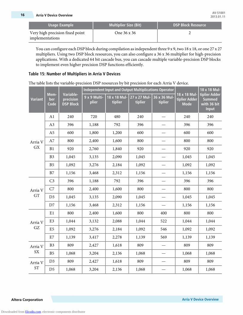
DSP Block ResourceMultiplier Size (Bit)Usage Example
2One 36 x 36Very high precision fixed pointimplementations
You can configure each DSP block during compilation as independent three 9 x 9, two 18 x 18, or one 27 x 27multipliers. Using two DSP block resources, you can also configure a 36 x 36 multiplier for high-precisionapplications. With a dedicated 64 bit cascade bus, you can cascade multiple variable-precision DSP blocksto implement even higher precision DSP functions efficiently.
Table 15: Number of Multipliers in Arria V Devices
The table lists the variable-precision DSP resources by bit precision for each Arria V device.18 x 18 Mul-tiplier Adder
Summedwith 36 bit
Input
18 x 18 Mul-tiplier Adder
Mode
Independent Input and Output Multiplications OperatorVariable-precisionDSP Block
Mem-ber
CodeVariant 36 x 36 Mul-
tiplier27 x 27 Mul-
tiplier18 x 18 Mul-
tiplier9 x 9 Multi-
plier
240240—240480720240A1
Arria VGX
396396—3967921,188396A3
600600—6001,2001,800600A5
800800—8001,6002,400800A7
920920—9201,8402,760920B1
1,0451,045—1,0452,0903,1351,045B3
1,0921,092—1,0922,1843,2761,092B5
1,1561,156—1,1562,3123,4681,156B7
396396—3967921,188396C3
Arria VGT
800800—8001,6002,400800C7
1,0451,045—1,0452,0903,1351,045D3
1,1561,156—1,1562,3123,4681,156D7
8008004008001,6002,400800E1
Arria VGZ
1,0441,0445221,0442,0883,1321,044E3
1,0921,0925461,0922,1843,2761,092E5
1,1391,1395691,1392,2783,4171,139E7
809809—8091,6182,427809B3Arria VSX 1,0681,068—1,0682,1363,2041,068B5
809809—8091,6182,427809D3Arria VST 1,0681,068—1,0682,1363,2041,068D5
Arria V Device OverviewAltera Corporation
AV-51001Arria V Device Overview16 2013.01.11
Downloaded from Elcodis.com electronic components distributor
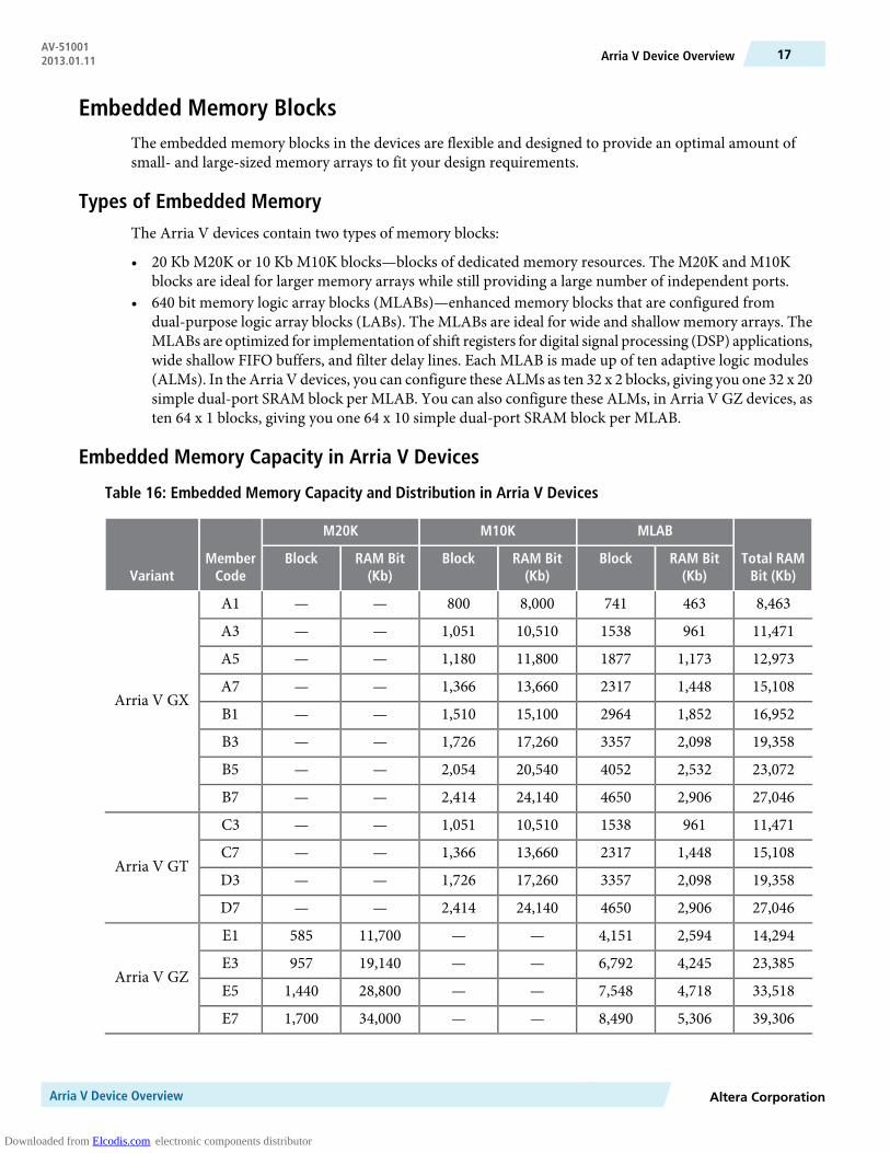
Embedded Memory BlocksThe embedded memory blocks in the devices are flexible and designed to provide an optimal amount ofsmall- and large-sized memory arrays to fit your design requirements.
Types of Embedded MemoryThe Arria V devices contain two types of memory blocks:
• 20 Kb M20K or 10 Kb M10K blocks—blocks of dedicated memory resources. The M20K and M10Kblocks are ideal for larger memory arrays while still providing a large number of independent ports.
• 640 bit memory logic array blocks (MLABs)—enhanced memory blocks that are configured fromdual-purpose logic array blocks (LABs). The MLABs are ideal for wide and shallow memory arrays. TheMLABs are optimized for implementation of shift registers for digital signal processing (DSP) applications,wide shallow FIFO buffers, and filter delay lines. Each MLAB is made up of ten adaptive logic modules(ALMs). In the Arria V devices, you can configure these ALMs as ten 32 x 2 blocks, giving you one 32 x 20simple dual-port SRAM block per MLAB. You can also configure these ALMs, in Arria V GZ devices, asten 64 x 1 blocks, giving you one 64 x 10 simple dual-port SRAM block per MLAB.
Embedded Memory Capacity in Arria V Devices
Table 16: Embedded Memory Capacity and Distribution in Arria V Devices
Total RAMBit (Kb)
MLABM10KM20K
MemberCodeVariant
RAM Bit(Kb)
BlockRAM Bit(Kb)
BlockRAM Bit(Kb)
Block
8,4634637418,000800——A1
Arria V GX
11,471961153810,5101,051——A3
12,9731,173187711,8001,180——A5
15,1081,448231713,6601,366——A7
16,9521,852296415,1001,510——B1
19,3582,098335717,2601,726——B3
23,0722,532405220,5402,054——B5
27,0462,906465024,1402,414——B7
11,471961153810,5101,051——C3
Arria V GT15,1081,448231713,6601,366——C7
19,3582,098335717,2601,726——D3
27,0462,906465024,1402,414——D7
14,2942,5944,151——11,700585E1
Arria V GZ23,3854,2456,792——19,140957E3
33,5184,7187,548——28,8001,440E5
39,3065,3068,490——34,0001,700E7
Altera CorporationArria V Device Overview
17Arria V Device OverviewAV-510012013.01.11
Downloaded from Elcodis.com electronic components distributor
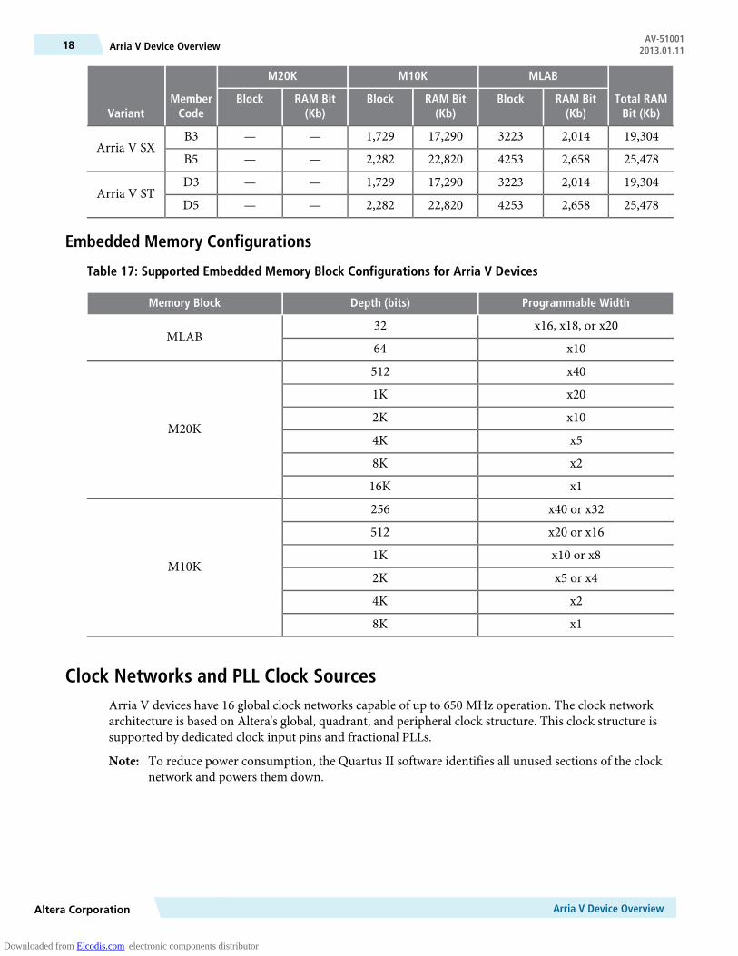
Total RAMBit (Kb)
MLABM10KM20K
MemberCodeVariant
RAM Bit(Kb)
BlockRAM Bit(Kb)
BlockRAM Bit(Kb)
Block
19,3042,014322317,2901,729——B3Arria V SX
25,4782,658425322,8202,282——B5
19,3042,014322317,2901,729——D3Arria V ST
25,4782,658425322,8202,282——D5
Embedded Memory Configurations
Table 17: Supported Embedded Memory Block Configurations for Arria V Devices
Programmable WidthDepth (bits)Memory Block
x16, x18, or x2032MLAB
x1064
x40512
M20K
x201K
x102K
x54K
x28K
x116K
x40 or x32256
M10K
x20 or x16512
x10 or x81K
x5 or x42K
x24K
x18K
Clock Networks and PLL Clock SourcesArria V devices have 16 global clock networks capable of up to 650 MHz operation. The clock networkarchitecture is based on Altera's global, quadrant, and peripheral clock structure. This clock structure issupported by dedicated clock input pins and fractional PLLs.
To reduce power consumption, the Quartus II software identifies all unused sections of the clocknetwork and powers them down.
Note:
Arria V Device OverviewAltera Corporation
AV-51001Arria V Device Overview18 2013.01.11
Downloaded from Elcodis.com electronic components distributor
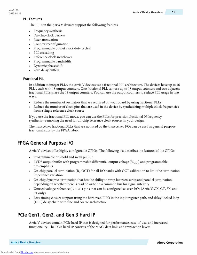
PLL Features
The PLLs in the Arria V devices support the following features:
• Frequency synthesis• On-chip clock deskew• Jitter attenuation• Counter reconfiguration• Programmable output clock duty cycles• PLL cascading• Reference clock switchover• Programmable bandwidth• Dynamic phase shift• Zero delay buffers
Fractional PLL
In addition to integer PLLs, the Arria V devices use a fractional PLL architecture. The devices have up to 16PLLs, each with 18 output counters. One fractional PLL can use up to 18 output counters and two adjacentfractional PLLs share the 18 output counters. You can use the output counters to reduce PLL usage in twoways:
• Reduce the number of oscillators that are required on your board by using fractional PLLs• Reduce the number of clock pins that are used in the device by synthesizing multiple clock frequencies
from a single reference clock source
If you use the fractional PLL mode, you can use the PLLs for precision fractional-N frequencysynthesis—removing the need for off-chip reference clock sources in your design.
The transceiver fractional PLLs that are not used by the transceiver I/Os can be used as general purposefractional PLLs by the FPGA fabric.
FPGA General Purpose I/OArria V devices offer highly configurable GPIOs. The following list describes the features of the GPIOs:
• Programmable bus hold and weak pull-up• LVDS output buffer with programmable differential output voltage (VOD ) and programmable
pre-emphasis• On-chip parallel termination (RT OCT) for all I/O banks with OCT calibration to limit the termination
impedance variation• On-chip dynamic termination that has the ability to swap between series and parallel termination,
depending on whether there is read or write on a common bus for signal integrity• Unused voltage reference ( VREF ) pins that can be configured as user I/Os (Arria V GX, GT, SX, and
ST only)• Easy timing closure support using the hard read FIFO in the input register path, and delay-locked loop
(DLL) delay chain with fine and coarse architecture
PCIe Gen1, Gen2, and Gen 3 Hard IPArria V devices contain PCIe hard IP that is designed for performance, ease-of-use, and increasedfunctionality. The PCIe hard IP consists of the MAC, data link, and transaction layers.
Altera CorporationArria V Device Overview
19Arria V Device OverviewAV-510012013.01.11
Downloaded from Elcodis.com electronic components distributor
The PCIe hard IP supports PCIe Gen3, Gen 2, and Gen 1 end point and root port for up to x8 laneconfiguration.
The PCIe endpoint support includes multifunction support for up to eight functions, as shown in thefollowing figure. The integrated multifunction support reduces the FPGA logic requirements by up to20,000 LEs for PCIe designs that require multiple peripherals.
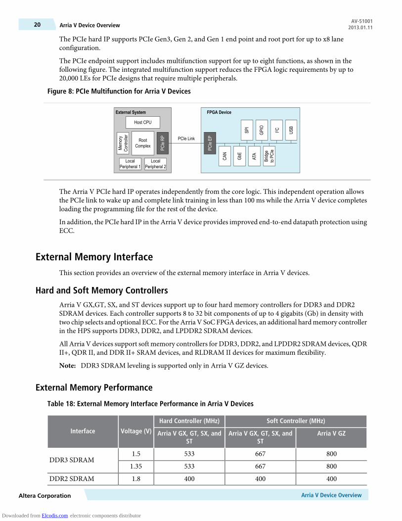
Figure 8: PCIe Multifunction for Arria V Devices
PCIe Link
External System FPGA Device
Host CPUMe
mory
Controller
RootComplex
LocalPeripheral 1
LocalPeripheral 2
PCIeRP
PCIeEP
CAN
GbE
ATA
Bridg
etoPC
Ie
SPI
GPIO
I2 C USB
The Arria V PCIe hard IP operates independently from the core logic. This independent operation allowsthe PCIe link to wake up and complete link training in less than 100 ms while the Arria V device completesloading the programming file for the rest of the device.
In addition, the PCIe hard IP in the Arria V device provides improved end-to-end datapath protection usingECC.
External Memory InterfaceThis section provides an overview of the external memory interface in Arria V devices.
Hard and Soft Memory ControllersArria V GX,GT, SX, and ST devices support up to four hard memory controllers for DDR3 and DDR2SDRAM devices. Each controller supports 8 to 32 bit components of up to 4 gigabits (Gb) in density withtwo chip selects and optional ECC. For theArria V SoC FPGAdevices, an additional hardmemory controllerin the HPS supports DDR3, DDR2, and LPDDR2 SDRAM devices.
All Arria V devices support soft memory controllers for DDR3, DDR2, and LPDDR2 SDRAM devices, QDRII+, QDR II, and DDR II+ SRAM devices, and RLDRAM II devices for maximum flexibility.
DDR3 SDRAM leveling is supported only in Arria V GZ devices.Note:
External Memory Performance
Table 18: External Memory Interface Performance in Arria V Devices
Soft Controller (MHz)Hard Controller (MHz)
Voltage (V)Interface Arria V GZArria V GX, GT, SX, andST
Arria V GX, GT, SX, andST
8006675331.5DDR3 SDRAM
8006675331.35
4004004001.8DDR2 SDRAM
Arria V Device OverviewAltera Corporation
AV-51001Arria V Device Overview20 2013.01.11
Downloaded from Elcodis.com electronic components distributor
Soft Controller (MHz)Hard Controller (MHz)
Voltage (V)Interface Arria V GZArria V GX, GT, SX, andST
Arria V GX, GT, SX, andST
—400—1.2LPDDR2 SDRAM
667——1.2RLDRAM 3
533400—1.8RLDRAM II
533400—1.5
500400—1.8QDR II+ SRAM
500400—1.5
333400—1.8QDR II SRAM
333400—1.5
—400—1.8DDR II+ SRAM21
—400—1.5
HPS External Memory Performance
Table 19: HPS External Memory Interface Performance
The hard processor system (HPS) is available in Arria V SoC FPGA devices only.HPS Hard Controller (MHz)Voltage (V)Interface
5331.5DDR3 SDRAM
5331.35
4001.8DDR2 SDRAM
4001.5
3331.2LPDDR2 SDRAM
Low-Power Serial TransceiversArria V devices deliver the industry's lowest power consumption per transceiver channel:
• 12.5 Gbps transceivers at less than 170 mW• 10 Gbps transceivers at less than 165 mW• 6 Gbps transceivers at less than 105 mW
Arria V transceivers are designed to be compliant with a wide range of protocols and data rates.
Transceiver ChannelsThe transceivers are positioned on the left and right outer edges of the device. The transceiver channelsconsist of the physical medium attachment (PMA), physical coding sublayer (PCS), and clock networks.
21 Not available as Altera® IP.
Altera CorporationArria V Device Overview
21Arria V Device OverviewAV-510012013.01.11
Downloaded from Elcodis.com electronic components distributor
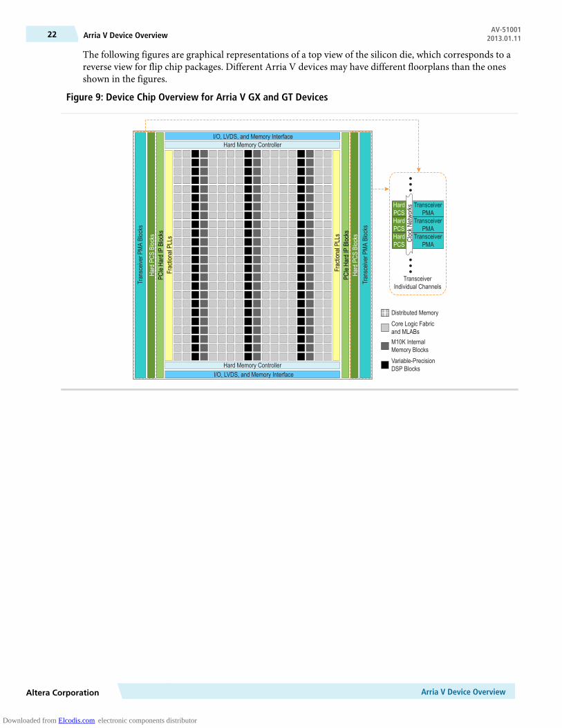
The following figures are graphical representations of a top view of the silicon die, which corresponds to areverse view for flip chip packages. Different Arria V devices may have different floorplans than the onesshown in the figures.
Figure 9: Device Chip Overview for Arria V GX and GT Devices
I/O, LVDS, and Memory Interface
I/O, LVDS, and Memory InterfaceTransceiv
erPM
ABlocks
Transceiv
erPM
ABlocks
HardPC
SBlocks
HardPC
SBlocks
PCIeHa
rdIP
Blocks
PCIeHa
rdIP
Blocks
FractionalPLLs
FractionalPLLs
Hard Memory Controller
Hard Memory Controller
Core Logic Fabricand MLABs
Variable-PrecisionDSP Blocks
M10K InternalMemory Blocks
Distributed Memory
TransceiverPMA
TransceiverPMA
TransceiverPMA
HardPCS
HardPCS
HardPCS
ClockN
etworks
TransceiverIndividual Channels
Arria V Device OverviewAltera Corporation
AV-51001Arria V Device Overview22 2013.01.11
Downloaded from Elcodis.com electronic components distributor
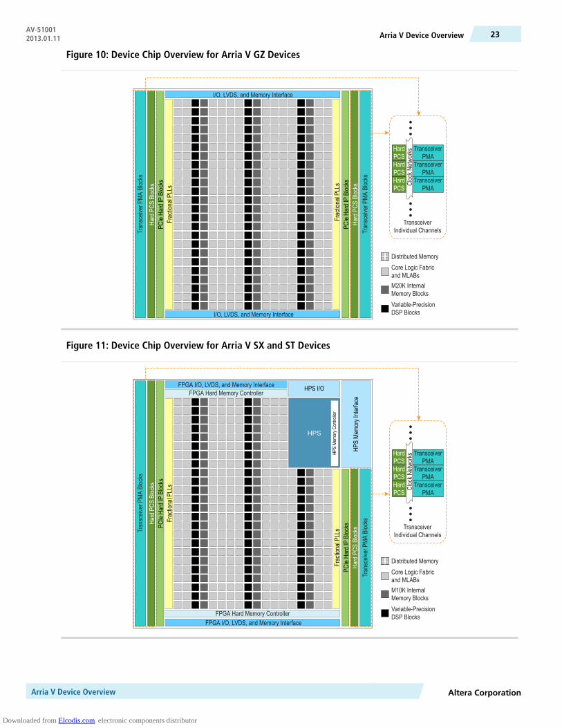
Figure 10: Device Chip Overview for Arria V GZ Devices
I/O, LVDS, and Memory Interface
I/O, LVDS, and Memory Interface
Transceiv
erPM
ABlocks
Transceiv
erPM
ABlocks
HardPC
SBlocks
HardPC
SBlocks
PCIeHa
rdIP
Blocks
PCIeHa
rdIP
Blocks
FractionalPLLs
FractionalPLLs
Core Logic Fabricand MLABs
Variable-PrecisionDSP Blocks
M20K InternalMemory Blocks
Distributed Memory
TransceiverPMA
TransceiverPMA
TransceiverPMA
HardPCS
HardPCS
HardPCS
ClockN
etworks
TransceiverIndividual Channels
Figure 11: Device Chip Overview for Arria V SX and ST Devices
FPGA I/O, LVDS, and Memory Interface
FPGA I/O, LVDS, and Memory Interface
Transceiv
erPM
ABlocks
Transceiv
erPM
ABlocksHardPC
SBlocks
HardPC
SBlocksPC
IeHa
rdIP
Blocks
PCIeHa
rdIP
Blocks
FractionalPLLs
FractionalPLLs
FPGA Hard Memory Controller
FPGA Hard Memory Controller
Core Logic Fabricand MLABs
Variable-PrecisionDSP Blocks
M10K InternalMemory Blocks
Distributed Memory
TransceiverPMA
TransceiverPMA
TransceiverPMA
HardPCS
HardPCS
HardPCS
ClockN
etworks
TransceiverIndividual Channels
HPSMe
moryCo
ntroller
HPS
HPS I/O
HPSMe
moryInterfac
e
Altera CorporationArria V Device Overview
23Arria V Device OverviewAV-510012013.01.11
Downloaded from Elcodis.com electronic components distributor
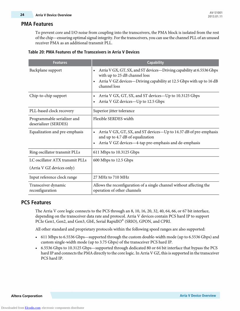
PMA FeaturesTo prevent core and I/O noise from coupling into the transceivers, the PMA block is isolated from the restof the chip—ensuring optimal signal integrity. For the transceivers, you can use the channel PLL of an unusedreceiver PMA as an additional transmit PLL.
Table 20: PMA Features of the Transceivers in Arria V Devices
CapabilityFeatures
• ArriaVGX,GT, SX, and STdevices—Driving capability at 6.5536Gbpswith up to 25 dB channel loss
• Arria V GZ devices—Driving capability at 12.5 Gbps with up to 16 dBchannel loss
Backplane support
• Arria V GX, GT, SX, and ST devices—Up to 10.3125 Gbps• Arria V GZ devices—Up to 12.5 Gbps
Chip-to-chip support
Superior jitter tolerancePLL-based clock recovery
Flexible SERDES widthProgrammable serializer anddeserializer (SERDES)
• Arria V GX, GT, SX, and ST devices—Up to 14.37 dB of pre-emphasisand up to 4.7 dB of equalization
• Arria V GZ devices—4-tap pre-emphasis and de-emphasis
Equalization and pre-emphasis
611 Mbps to 10.3125 GbpsRing oscillator transmit PLLs
600 Mbps to 12.5 GbpsLC oscillator ATX transmit PLLs
(Arria V GZ devices only)
27 MHz to 710 MHzInput reference clock range
Allows the reconfiguration of a single channel without affecting theoperation of other channels
Transceiver dynamicreconfiguration
PCS FeaturesThe Arria V core logic connects to the PCS through an 8, 10, 16, 20, 32, 40, 64, 66, or 67 bit interface,depending on the transceiver data rate and protocol. Arria V devices contain PCS hard IP to supportPCIe Gen1, Gen2, and Gen3, GbE, Serial RapidIO® (SRIO), GPON, and CPRI.
All other standard and proprietary protocols within the following speed ranges are also supported:
• 611 Mbps to 6.5536 Gbps—supported through the custom double-width mode (up to 6.5536 Gbps) andcustom single-width mode (up to 3.75 Gbps) of the transceiver PCS hard IP.
• 6.5536 Gbps to 10.3125 Gbps—supported through dedicated 80 or 64 bit interface that bypass the PCShard IP and connects the PMAdirectly to the core logic. In Arria VGZ, this is supported in the transceiverPCS hard IP.
Arria V Device OverviewAltera Corporation
AV-51001Arria V Device Overview24 2013.01.11
Downloaded from Elcodis.com electronic components distributor
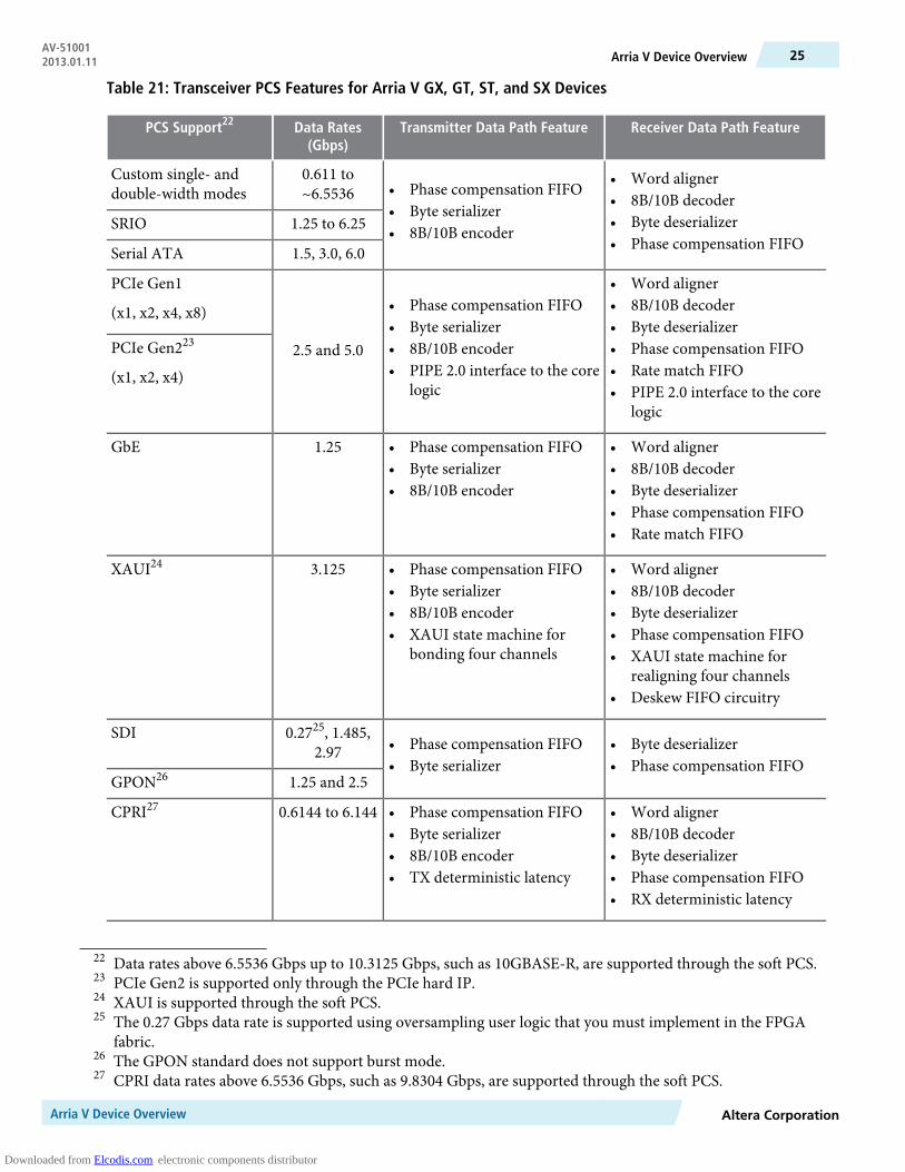
Table 21: Transceiver PCS Features for Arria V GX, GT, ST, and SX Devices
Receiver Data Path FeatureTransmitter Data Path FeatureData Rates(Gbps)
PCS Support22
• Word aligner• 8B/10B decoder• Byte deserializer• Phase compensation FIFO
• Phase compensation FIFO• Byte serializer• 8B/10B encoder
0.611 to~6.5536
Custom single- anddouble-width modes
1.25 to 6.25SRIO
1.5, 3.0, 6.0Serial ATA
• Word aligner• 8B/10B decoder• Byte deserializer• Phase compensation FIFO• Rate match FIFO• PIPE 2.0 interface to the core
logic
• Phase compensation FIFO• Byte serializer• 8B/10B encoder• PIPE 2.0 interface to the core
logic
2.5 and 5.0
PCIe Gen1
(x1, x2, x4, x8)
PCIe Gen223
(x1, x2, x4)
• Word aligner• 8B/10B decoder• Byte deserializer• Phase compensation FIFO• Rate match FIFO
• Phase compensation FIFO• Byte serializer• 8B/10B encoder
1.25GbE
• Word aligner• 8B/10B decoder• Byte deserializer• Phase compensation FIFO• XAUI state machine for
realigning four channels• Deskew FIFO circuitry
• Phase compensation FIFO• Byte serializer• 8B/10B encoder• XAUI state machine for
bonding four channels
3.125XAUI24
• Byte deserializer• Phase compensation FIFO
• Phase compensation FIFO• Byte serializer
0.2725, 1.485,2.97
SDI
1.25 and 2.5GPON26
• Word aligner• 8B/10B decoder• Byte deserializer• Phase compensation FIFO• RX deterministic latency
• Phase compensation FIFO• Byte serializer• 8B/10B encoder• TX deterministic latency
0.6144 to 6.144CPRI27
22 Data rates above 6.5536 Gbps up to 10.3125 Gbps, such as 10GBASE-R, are supported through the soft PCS.23 PCIe Gen2 is supported only through the PCIe hard IP.24 XAUI is supported through the soft PCS.25 The 0.27 Gbps data rate is supported using oversampling user logic that you must implement in the FPGA
fabric.26 The GPON standard does not support burst mode.27 CPRI data rates above 6.5536 Gbps, such as 9.8304 Gbps, are supported through the soft PCS.
Altera CorporationArria V Device Overview
25Arria V Device OverviewAV-510012013.01.11
Downloaded from Elcodis.com electronic components distributor
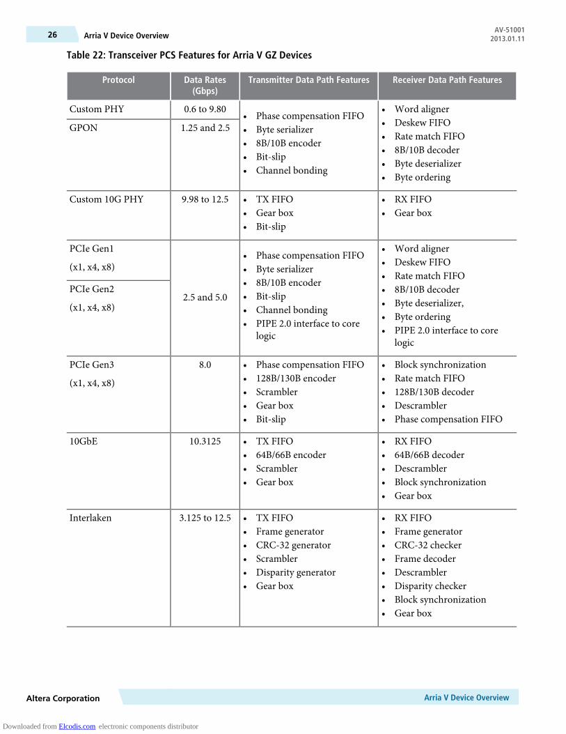
Table 22: Transceiver PCS Features for Arria V GZ Devices
Receiver Data Path FeaturesTransmitter Data Path FeaturesData Rates(Gbps)
Protocol
• Word aligner• Deskew FIFO• Rate match FIFO• 8B/10B decoder• Byte deserializer• Byte ordering
• Phase compensation FIFO• Byte serializer• 8B/10B encoder• Bit-slip• Channel bonding
0.6 to 9.80Custom PHY
1.25 and 2.5GPON
• RX FIFO• Gear box
• TX FIFO• Gear box• Bit-slip
9.98 to 12.5Custom 10G PHY
• Word aligner• Deskew FIFO• Rate match FIFO• 8B/10B decoder• Byte deserializer,• Byte ordering• PIPE 2.0 interface to core
logic
• Phase compensation FIFO• Byte serializer• 8B/10B encoder• Bit-slip• Channel bonding• PIPE 2.0 interface to core
logic
2.5 and 5.0
PCIe Gen1
(x1, x4, x8)
PCIe Gen2
(x1, x4, x8)
• Block synchronization• Rate match FIFO• 128B/130B decoder• Descrambler• Phase compensation FIFO
• Phase compensation FIFO• 128B/130B encoder• Scrambler• Gear box• Bit-slip
8.0PCIe Gen3
(x1, x4, x8)
• RX FIFO• 64B/66B decoder• Descrambler• Block synchronization• Gear box
• TX FIFO• 64B/66B encoder• Scrambler• Gear box
10.312510GbE
• RX FIFO• Frame generator• CRC-32 checker• Frame decoder• Descrambler• Disparity checker• Block synchronization• Gear box
• TX FIFO• Frame generator• CRC-32 generator• Scrambler• Disparity generator• Gear box
3.125 to 12.5Interlaken
Arria V Device OverviewAltera Corporation
AV-51001Arria V Device Overview26 2013.01.11
Downloaded from Elcodis.com electronic components distributor
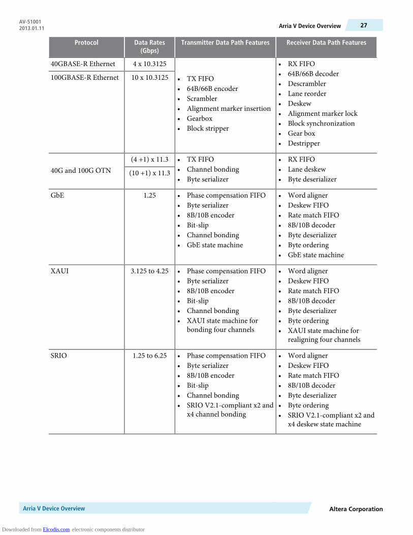
Receiver Data Path FeaturesTransmitter Data Path FeaturesData Rates(Gbps)
Protocol
• RX FIFO• 64B/66B decoder• Descrambler• Lane reorder• Deskew• Alignment marker lock• Block synchronization• Gear box• Destripper
• TX FIFO• 64B/66B encoder• Scrambler• Alignment marker insertion• Gearbox• Block stripper
4 x 10.312540GBASE-R Ethernet
10 x 10.3125100GBASE-R Ethernet
• RX FIFO• Lane deskew• Byte deserializer
• TX FIFO• Channel bonding• Byte serializer
(4 +1) x 11.340G and 100G OTN (10 +1) x 11.3
• Word aligner• Deskew FIFO• Rate match FIFO• 8B/10B decoder• Byte deserializer• Byte ordering• GbE state machine
• Phase compensation FIFO• Byte serializer• 8B/10B encoder• Bit-slip• Channel bonding• GbE state machine
1.25GbE
• Word aligner• Deskew FIFO• Rate match FIFO• 8B/10B decoder• Byte deserializer• Byte ordering• XAUI state machine for
realigning four channels
• Phase compensation FIFO• Byte serializer• 8B/10B encoder• Bit-slip• Channel bonding• XAUI state machine for
bonding four channels
3.125 to 4.25XAUI
• Word aligner• Deskew FIFO• Rate match FIFO• 8B/10B decoder• Byte deserializer• Byte ordering• SRIO V2.1-compliant x2 and
x4 deskew state machine
• Phase compensation FIFO• Byte serializer• 8B/10B encoder• Bit-slip• Channel bonding• SRIO V2.1-compliant x2 and
x4 channel bonding
1.25 to 6.25SRIO
Altera CorporationArria V Device Overview
27Arria V Device OverviewAV-510012013.01.11
Downloaded from Elcodis.com electronic components distributor
SoC FPGA with HPSEach SoC FPGA combines an FPGA fabric and an HPS in a single device. This combination delivers theflexibility of programmable logic with the power and cost savings of hard IP in these ways:
• Reduces board space, systempower, and bill ofmaterials cost by eliminating a discrete embedded processor• Allows you to differentiate the end product in both hardware and software, and to support virtually any
interface standard• Extends the product life and revenue through in-field hardware and software updates
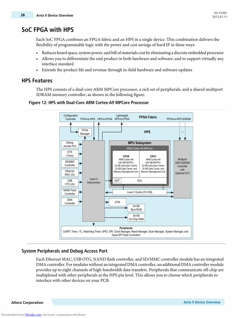
HPS FeaturesThe HPS consists of a dual-core ARM MPCore processor, a rich set of peripherals, and a shared multiportSDRAM memory controller, as shown in the following figure.
Figure 12: HPS with Dual-Core ARM Cortex-A9 MPCore Processor
FPGA Fabric
HPS
HPS-to-FPGALightweight
HPS-to-FPGAFPGA-to-HPS FPGA-to-HPS SDRAMConfigurationController
FPGAManager
64 KBOn-Chip RAM
64 KBBoot ROM
Level 3Interconnect
EthernetMAC (2x)
USBOTG (2x)
NAND FlashController
SD/MMCController
DMAController STM
ETR(Trace)
DebugAccess Port
ARM Cortex-A9 MPCore
MPU Subsystem
CPU0ARM Cortex-A9with NEON/FPU,
32 KB Instruction Cache,32 KB Data Cache, and
Memory Management Unit
CPU1ARM Cortex-A9with NEON/FPU,
32 KB Instruction Cache,32 KB Data Cache, and
Memory Management Unit
SCUACP
Level 2 Cache (512 KB)
MultiportDDR SDRAMController
withOptional ECC
Peripherals(UART, Timer, I 2C, Watchdog Timer, GPIO, SPI, Clock Manager, Reset Manager, Scan Manager, System Manager, and
Quad SPI Flash Controller)
System Peripherals and Debug Access Port
Each Ethernet MAC, USB OTG, NAND flash controller, and SD/MMC controller module has an integratedDMAcontroller. Formoduleswithout an integratedDMAcontroller, an additionalDMAcontrollermoduleprovides up to eight channels of high-bandwidth data transfers. Peripherals that communicate off-chip aremultiplexed with other peripherals at the HPS pin level. This allows you to choose which peripherals tointerface with other devices on your PCB.
Arria V Device OverviewAltera Corporation
AV-51001Arria V Device Overview28 2013.01.11
Downloaded from Elcodis.com electronic components distributor
The debug access port provides interfaces to industry standard JTAG debug probes and supports ARMCoreSight debug and core traces to facilitate software development.
HPS–FPGA AXI Bridges
TheHPS–FPGAbridges, which support theAdvancedMicrocontroller BusArchitecture (AMBA®)AdvancedeXtensible Interface (AXI™) specifications, consist of the following bridges:
• FPGA-to-HPS AXI bridge—a high-performance bus supporting 32, 64, and 128 bit data widths thatallows the FPGA fabric to issue transactions to slaves in the HPS.
• HPS-to-FPGA AXI bridge—a high-performance bus supporting 32, 64, and 128 bit data widths thatallows the HPS to issue transactions to slaves in the FPGA fabric.
• Lightweight HPS-to-FPGA AXI bridge—a lower performance 32 bit width bus that allows the HPS toissue transactions to slaves in the FPGA fabric. This bridge is primarily used for control and status register(CSR) accesses to peripherals in the FPGA fabric.
The HPS–FPGA AXI bridges allow masters in the FPGA fabric to communicate with slaves in the HPS logic,and vice versa. For example, the HPS-to-FPGA AXI bridge allows you to share memories instantiated in theFPGA fabric with one or both microprocessors in the HPS, while the FPGA-to-HPS AXI bridge allows logicin the FPGA fabric to access the memory and peripherals in the HPS.
Each HPS–FPGA bridge also provides asynchronous clock crossing for data transferred between the FPGAfabric and the HPS.
HPS SDRAM Controller Subsystem
The HPS SDRAM controller subsystem contains a multiport SDRAM controller and DDR PHY that areshared between the FPGA fabric (through the FPGA-to-HPS SDRAM interface), the level 2 (L2) cache, andthe level 3 (L3) system interconnect. The FPGA-to-HPS SDRAM interface supports AMBAAXI andAvalon®
Memory-Mapped (Avalon-MM) interface standards, and provides up to six individual ports for access bymasters implemented in the FPGA fabric.
To maximize memory performance, the SDRAM controller subsystem supports command and datareordering, deficit round-robin arbitration with aging, and high-priority bypass features. The SDRAMcontroller subsystem supports DDR2, DDR3, or LPDDR2 devices up to 4 Gb in density operating at up to533 MHz (1066 Mbps data rate).
FPGA Configuration and Processor BootingThe FPGA fabric andHPS in the SoCFPGAare powered independently. You can reduce the clock frequenciesor gate the clocks to reduce dynamic power, or shut down the entire FPGA fabric to reduce total systempower.
You can configure the FPGA fabric and boot the HPS independently, in any order, providing you with moredesign flexibility:
• You can boot theHPS independently. After theHPS is running, theHPS can fully or partially reconfigurethe FPGA fabric at any time under software control. The HPS can also configure other FPGAs on theboard through the FPGA configuration controller.
• You can power up both the HPS and the FPGA fabric together, configure the FPGA fabric first, and thenboot the HPS from memory accessible to the FPGA fabric.
Although the FPGA fabric and HPS are on separate power domains, the HPS must remain poweredup during operation while the FPGA fabric can be powered up or down as required.
Note:
Altera CorporationArria V Device Overview
29Arria V Device OverviewAV-510012013.01.11
Downloaded from Elcodis.com electronic components distributor
Hardware and Software DevelopmentFor hardware development, you can configure the HPS and connect your soft logic in the FPGA fabric tothe HPS interfaces using the Qsys system integration tool in the Quartus II software.
For software development, the ARM-based SoC FPGA devices inherit the rich software developmentecosystem available for the ARM Cortex-A9 MPCore processor. The software development process forAltera SoC FPGAs follows the same steps as those for other SoC devices from other manufacturers. Supportfor Linux, VxWorks®, and other operating systemswill be available for the SoCFPGAs. Formore informationon the operating systems support availability, contact the Altera sales team.
You can begin device-specific firmware and software development on the Altera SoC FPGA Virtual Target.The Virtual Target is a fast PC-based functional simulation of a target development system—a model of acomplete development board that runs on a PC. TheVirtual Target enables the development of device-specificproduction software that can run unmodified on actual hardware.
Dynamic and Partial ReconfigurationThe Arria V devices support dynamic reconfiguration and partial reconfiguration.
Dynamic ReconfigurationThe dynamic reconfiguration feature allows you to dynamically change the transceiver data rates, PMAsettings, or protocols of a channel, without affecting data transfer on adjacent channels. This feature is idealfor applications that require on-the-fly multiprotocol or multirate support. You can reconfigure the PMA,PCS, and PCIe hard IP blocks with dynamic reconfiguration.
Partial ReconfigurationPartial reconfiguration allows you to reconfigure part of the device while other sections of the device remainoperational. This capability is important in systems with critical uptime requirements because it allows youto make updates or adjust functionality without disrupting services.
Apart from lowering cost and power consumption, partial reconfiguration increases the effective logic densityof the device because placing device functions that do not operate simultaneously is not necessary. Instead,you can store these functions in external memory and load them whenever the functions are required. Thiscapability reduces the size of the device because it allows multiple applications on a single device—savingthe board space and reducing the power consumption.
Altera simplifies the time-intensive task of partial reconfiguration by building this capability on top of theproven incremental compile and design flow in the Quartus II design software. With the Altera® solution,you do not need to know all the intricate device architecture details to perform a partial reconfiguration.
Partial reconfiguration is supported through the FPP x16 configuration interface. You can seamlessly usepartial reconfiguration in tandemwith dynamic reconfiguration to enable simultaneous partial reconfigurationof both the device core and transceivers.
Arria V Device OverviewAltera Corporation
AV-51001Arria V Device Overview30 2013.01.11
Downloaded from Elcodis.com electronic components distributor
Enhanced Configuration and Configuration via Protocol
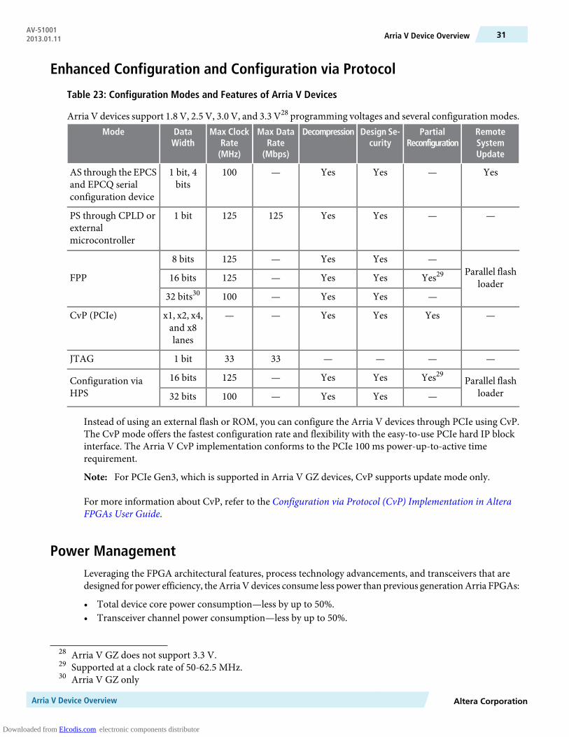
Table 23: Configuration Modes and Features of Arria V Devices
Arria V devices support 1.8 V, 2.5 V, 3.0 V, and 3.3 V28 programming voltages and several configuration modes.RemoteSystemUpdate
PartialReconfiguration
Design Se-curity
DecompressionMax DataRate
(Mbps)
Max ClockRate(MHz)
DataWidth
Mode
Yes—YesYes—1001 bit, 4bits
AS through the EPCSand EPCQ serialconfiguration device
——YesYes1251251 bitPS through CPLD orexternalmicrocontroller
Parallel flashloader
—YesYes—1258 bits
FPP Yes29YesYes—12516 bits
—YesYes—10032 bits30
—YesYesYes——x1, x2, x4,and x8lanes
CvP (PCIe)
————33331 bitJTAG
Parallel flashloader
Yes29YesYes—12516 bitsConfiguration viaHPS —YesYes—10032 bits
Instead of using an external flash or ROM, you can configure the Arria V devices through PCIe using CvP.The CvP mode offers the fastest configuration rate and flexibility with the easy-to-use PCIe hard IP blockinterface. The Arria V CvP implementation conforms to the PCIe 100 ms power-up-to-active timerequirement.
For PCIe Gen3, which is supported in Arria V GZ devices, CvP supports update mode only.Note:
For more information about CvP, refer to the Configuration via Protocol (CvP) Implementation in AlteraFPGAs User Guide.
Power ManagementLeveraging the FPGA architectural features, process technology advancements, and transceivers that aredesigned for power efficiency, theArriaV devices consume less power than previous generationArria FPGAs:
• Total device core power consumption—less by up to 50%.• Transceiver channel power consumption—less by up to 50%.
28 Arria V GZ does not support 3.3 V.29 Supported at a clock rate of 50-62.5 MHz.30 Arria V GZ only
Altera CorporationArria V Device Overview
31Arria V Device OverviewAV-510012013.01.11
Downloaded from Elcodis.com electronic components distributor
Additionally, Arria V devices contain several hard IP blocks, including PCIe Gen1, Gen2, and Gen3, GbE,SRIO, GPON, and CPRI protocols, that reduce logic resources and deliver substantial power savings of upto 25% less power than equivalent soft implementations.
Document Revision History
ChangesVersionDate
• Added the L optional suffix to the Arria V GZ ordering code for the-I3 speed grade.
• Added a note about the power-up sequence requirement if you planto migrate your design from the Arria V GX A5 and A7, and Arria VGT C7 devices to other Arria V devices.
2013.01.11January 2013
• Updated the summary of features.• Updated Arria V GZ information regarding 3.3 V I/O support.• Removed Arria V GZ engineering sample ordering code.• Updated the maximum resource counts for Arria V GX and GZ.• Updated Arria V ST ordering codes for transceiver count.• Updated transceiver counts for Arria V ST packages.• Added simplified floorplan diagrams for Arria V GZ, SX, and ST.• Added FPP x32 configuration mode for Arria V GZ only.• Updated CvP (PCIe) remote system update support information.• Added HPS external memory performance information.• Updated template.
2012.11.19November 2012
• Added Arria V GZ information.• Updated Table 1, Table 2, Table 3, Table 14, Table 15, Table 16, Table
17, Table 18, Table 19, Table 20, and Table 21.• Added the “Arria V GZ” section.• Added Table 8, Table 9 and Table 22.
3.0October 2012
• Added –I3 speed grade to Figure 1 for Arria V GX devices.• Updated the 6-Gbps transceiver speed from6.553Gbps to 6.5536Gbps
in Figure 3 and Figure 1.
2.1July 2012
• Restructured the document.• Added the “Embedded Memory Capacity” and “Embedded Memory
Configurations” sections.• Added Table 1, Table 3, Table 12, Table 15, and Table 16.• Updated Table 2, Table 4, Table 5, Table 6, Table 7, Table 8, Table 9,
Table 10, Table 11, Table 13, Table 14, and Table 19.• Updated Figure 1, Figure 2, Figure 3, Figure 4, and Figure 8.• Updated the “FPGA Configuration and Processor Booting” and
“Hardware and Software Development” sections.• Text edits throughout the document.
2.0June 2012
Arria V Device OverviewAltera Corporation
AV-51001Arria V Device Overview32 2013.01.11
Downloaded from Elcodis.com electronic components distributor
ChangesVersionDate
• Updated Table 1–7 and Table 1–8.• Updated Figure 1–9 and Figure 1–10.• Minor text edits.
1.3February 2012
Minor text edits.1.2December 2011
• Updated Table 1–1, Table 1–2, Table 1–3, Table 1–4, Table 1–6, Table1–7, Table 1–9, and Table 1–10.
• Added “SoC FPGA with HPS” section.• Updated “Clock Networks and PLL Clock Sources” and “Ordering
Information” sections.• Updated Figure 1–5.• Added Figure 1–6.• Minor text edits.
1.1November 2011
Initial release.1.0August 2011
Altera CorporationArria V Device Overview
33Arria V Device OverviewAV-510012013.01.11
Downloaded from Elcodis.com electronic components distributor