![[XLS]cbse.gov.incbse.gov.in/pr_rti/RTI-Inward-Outward_Upto_Jun_2012_ro... · Web viewAnuroop Nair, C-32, Abeanzer School, Govind puri, Gwalior Kameshwar Ram, Srigar Kalri, Anuppur-](https://static.fdocuments.net/doc/165x107/5aff98167f8b9a84338b6b82/xlscbsegov-viewanuroop-nair-c-32-abeanzer-school-govind-puri-gwalior-kameshwar.jpg)
Kameshwar Poolla Mechanical Engineering Electrical Engineering & CS University of California,...
36
Kameshwar Poolla Mechanical Engineering Electrical Engineering & CS University of California, Berkeley April 10, 2006 Wireless Metrology and Process Control for Semiconductor Manufacturing This research was supported by NSF, UC SMART, & gifts from Intel, AMD, Novellus, Applied Materials, Cypress, Lam Research, TEL, Nikon.
-
date post
21-Dec-2015 -
Category
Documents
-
view
215 -
download
1
Transcript of Kameshwar Poolla Mechanical Engineering Electrical Engineering & CS University of California,...

Kameshwar PoollaMechanical Engineering
Electrical Engineering & CSUniversity of California, Berkeley
April 10, 2006
Wireless Metrology and Process Control for Semiconductor Manufacturing
This research was supported by NSF, UC SMART, & gifts from Intel, AMD, Novellus, Applied Materials, Cypress, Lam Research, TEL, Nikon.

04/18/2304/18/23 22
semiconductor semiconductor
manufacturing manufacturing
backgroundbackground

04/18/23 slide 3
What is it?
• Selective deposition &
selective removal of
various materials to form ICs• Selectivity is done by protecting
desired areas with resist
IBM Power PC750
04/18/23 slide 4
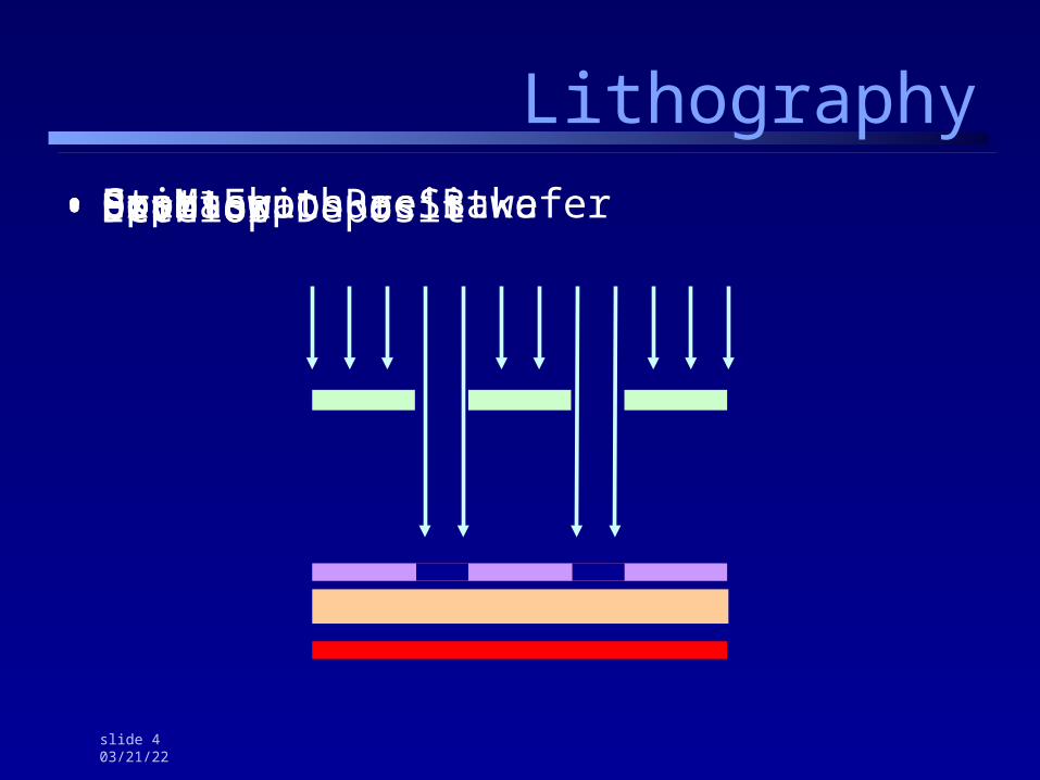
Lithography• Start with a Si wafer• Spin-coat Resist• Cr Mask • Expose• Post Exposure Bake• Develop• Etch or Deposit

04/18/23 slide 5
Process Overview
Resist
PAB
Scanner
Develop
Production
Wafer Flow
PEB
PDB
Etch
Track
Photomask

04/18/23 slide 6
Critical Dimension (CD)
• Captures quality of pattern transfer
• CD Target – desired width of printed lines• CD(x,y) – actual width of printed lines • Depends on (x,y)
because process varies across wafer
• Measured on test wafers
using CD SEM or Scatterometry
04/18/23 slide 7
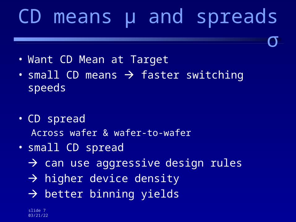
CD means μ and spreads σ
• Want CD Mean at Target• small CD means faster switching speeds
• CD spreadAcross wafer & wafer-to-wafer
• small CD spread
can use aggressive design rules
higher device density
better binning yields

04/18/23 slide 8
Good
Bad

04/18/23 slide 9
Yield
Binning
Post OnWafer Optimization
6nm
Bin 2Bin 3Device/Fab
Economics
Bin 1
$
Intel P4 Prices:
3.8 GHz - $429
3.2 GHz - $336
2.8 GHz - $279
Typical CD Distribution
11nm
Target CD
Improved Yield & Bin Sort = $$$
Yield

04/18/23 slide 10
Post Exposure Bake
• Key step – greatly influences CD μ and • Makes exposed resist diffuse• To reduce standing wave patterns• Gives better pattern transfer
• Must be very accurately controlled• State-of-the-art
±0.3 ºC across 300 mm wafer

04/18/23 slide 11
PEB reduces Standing Waves
Courtesy of CNF, Cornell University

04/18/23 slide 12
Our Plan ~1997
• Decided to do Control of Lithography
• Feedback Control requiresSensors & Actuators
• Available Actuation?Plenty – exposure dose, focal plane, PEB Temp
• Available Sensors in Lithography?Not many and pretty useless for control

04/18/23 slide 13
Need in situ Sensing
What was the state of the wafer during processing?
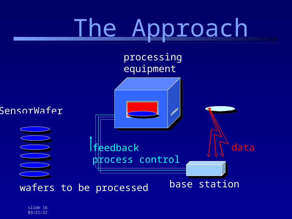
processingequipmentwafers to
be processedfinished
wafer

04/18/23 slide 14
in situ Sensing• Need wafer-state information
– Temperature in post-exposure bake– Latent image in lithographic exposure– Etch rate of wafer in plasma etch– Deposition rate in CVD processes
• The Big Problems– Chamber access– Deployment cost
04/18/23 slide 15
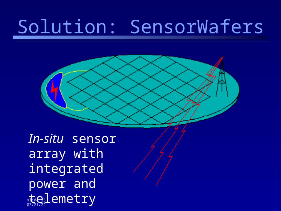
In-situ sensor array with integrated power and telemetry
Solution: SensorWafers
04/18/23 slide 16
feedbackprocess control
processingequipment
data
SensorWafer
base station
The Approach
wafers to be processed
04/18/23 slide 17
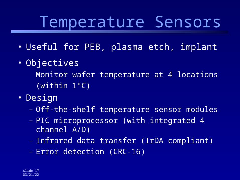
Temperature Sensors
• Useful for PEB, plasma etch, implant
• ObjectivesMonitor wafer temperature at 4 locations
(within 1ºC)
• Design– Off-the-shelf temperature sensor modules– PIC microprocessor (with integrated 4 channel A/D)– Infrared data transfer (IrDA compliant)– Error detection (CRC-16)

04/18/23 slide 18
Early attempts …
Ir-LED
P
Batteries
SensorIr-LED
P
Batteries
Sensor
Problems: clearance, isolation, contamination & they are ugly !

04/18/23 slide 19
Etch Rate Sensor
• Sensor to measure polysilicon etch rate• Based on van der Pauw probe electrical film-
thickness measurement:
I
I
Poly-Si
V
04/18/23 slide 20
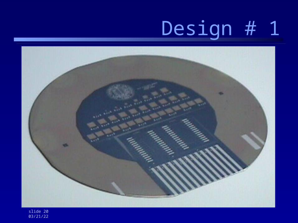
Design # 1
04/18/23 slide 21
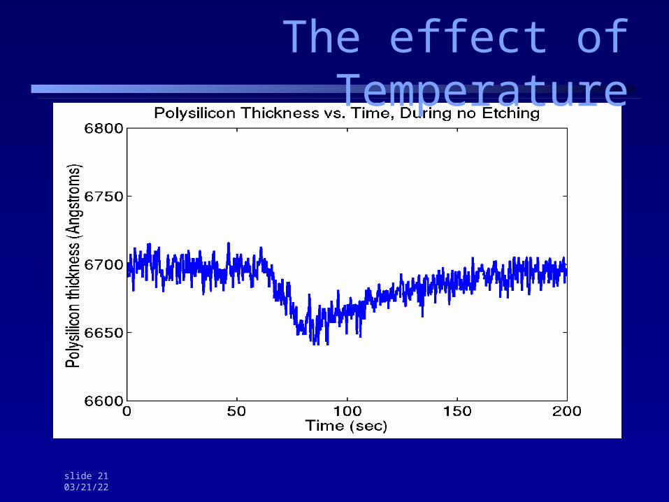
The effect of Temperature

04/18/23 slide 22
Results
Problems: clearance, isolation, contamination

04/18/23 slide 23
Thermal Flux Sensors
• Plasma etch is highly sensitive to wafer temp
etch rate, selectivity, and anisotropy• Heat delivered to the wafer has two sources
– Ion flux bombardment
Indirect measure of physical etch– Exothermic chemical etch reactions
Indirect measure of chemical etch
• Want to resolve these heat fluxes– Can deduce sidewall, anisotropy etc.
04/18/23 slide 24
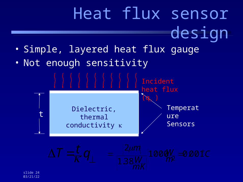
Heat flux sensor design
qtT
• Simple, layered heat flux gauge• Not enough sensitivity
Dielectric, thermal conductivity
Temperature Sensorst
Incident heat flux (q )
CmW
mKW
m
001.0100038.1
22
04/18/23 slide 25
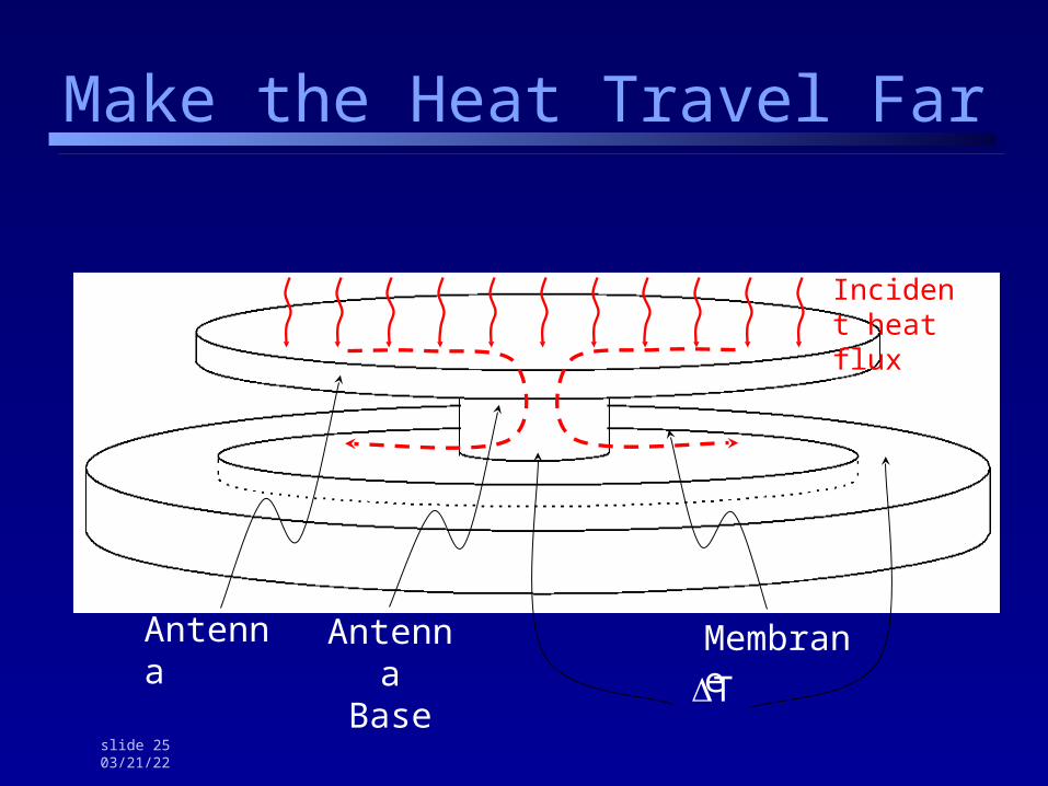
Make the Heat Travel Far
Incident heat flux
Antenna
Antenna
Base
MembraneT

04/18/23 slide 26
MembraneTop View
D
MembraneSide View
Heat flow within thin dielectric membrane
T
Antenna / Membrane Structure
b
T
Heat sink
Heat sink
Heat flow
Incident heat
bD
kwDqT ln8
2
C4 T

04/18/23 slide 27
• Discrimination between
physical and chemical sources• Use two heat flux sensors:
one exposed, one covered– Exposed sensor is heated by both sources– Covered sensor receives only physical heating
Heat Flux Resolution

04/18/23 slide 28
• Membrane: Silicon nitride
• Antenna: SiO2 / Aluminum
• Plasma-etched material: resist (O2 plasma)
• Temperature sensors: polysilicon• Tethered power and communication
Design #1
Heat sink Heat sink
Si
AlPR
SiO2
Si3N
4
poly

04/18/23 slide 29
Layout – Wheatstone Bridge
Etched Sensor
Non-Etched
Non-Etched

04/18/23 slide 30
Layout – Full Die (20 per wafer)
EdgeboardConnector
Sensors

04/18/23 slide 31
• Antenna: Undoped polysilicon (low )• Linewidths: increased • Tethered power and communication
Design # 2
Heat sink Heat sink
Si
PR
poly
Si3N
4
poly

04/18/23 slide 32
Final Design

04/18/23 slide 33
Testing
• Test sensors on the “bench”– Use an off-the-shelf heat flux sensor and a heating element
to compare readings:
Aluminum heat sink
off-the-shelf sensor
sensor
heater
vacuum chamber

04/18/23 slide 34
Bench-top Results

04/18/23 slide 35
Going up the food chain
• Sensors become rapidly commodified• Value is in using the data• This is through Control, Modeling, Optimization
• Examples– Equipment Control– Fault Detection and Isolation– Process Optimization

04/18/23 slide 36
The Value of Control
• PEB Example• Control spatial temperature of bake plate • Yesterday ± 0.3 °C • Today ± 0.15 °C • Result: 1 nm reduction in CD spread• Benefit: mid-sized fab in 1st year of product lifecycle
~$3/die * 200 die/wafer * 20,000 wafer/mon * 12 mon/yr
• 144 M$ per year !!


![Cyber Security for Smart Grid Devices - TCIPG · Applications Symposium2008 ] Optimal Contracts for Wind Power Producers in Electricity Markets (Poolla) [CDC 2010] Renewable integration](https://static.fdocuments.net/doc/165x107/5f05517a7e708231d4125ec8/cyber-security-for-smart-grid-devices-tcipg-applications-symposium2008-optimal.jpg)


