Junction Mixing Scanning Tunneling Microscopy - University of Alberta
196
University of Alberta Library Release Form Name of Author: Geoffrey Mark Steeves Title of Thesis: Junction Mixing Scanning Tunneling Microscopy Degree: Doctor of Philosophy Year this Degree Granted: 2001 Permission is hereby granted to the University of Alberta Library to reproduce single copies of this thesis and to lend or sell such copies for private, scholarly or scientific research purposes only. The author reserves all other publication and other rights in association with the copyright in the thesis, and except as hereinbefore provided, neither the thesis nor any substantial portion thereof may be printed or otherwise reproduced in any material form whatever without the author’s prior written permission. . . . . . . . . . . . . . . . . . . . Geoffrey Mark Steeves Department of Physics University of Alberta Edmonton, AB Canada, T6G 2J1 Date: . . . . . . . . .
Transcript of Junction Mixing Scanning Tunneling Microscopy - University of Alberta

University of Alberta
Library Release Form
Name of Author: Geoffrey Mark Steeves
Title of Thesis: Junction Mixing Scanning Tunneling Microscopy
Degree: Doctor of Philosophy
Year this Degree Granted: 2001
Permission is hereby granted to the University of Alberta Library to reproduce single copiesof this thesis and to lend or sell such copies for private, scholarly or scientific researchpurposes only.
The author reserves all other publication and other rights in association with the copyrightin the thesis, and except as hereinbefore provided, neither the thesis nor any substantialportion thereof may be printed or otherwise reproduced in any material form whateverwithout the author’s prior written permission.
. . . . . . . . . . . . . . . . . . .Geoffrey Mark SteevesDepartment of PhysicsUniversity of AlbertaEdmonton, ABCanada, T6G 2J1
Date: . . . . . . . . .

University of Alberta
Junction Mixing Scanning Tunneling Microscopy
by
Geoffrey Mark Steeves
A thesis submitted to the Faculty of Graduate Studies and Research in partial fulfillmentof the requirements for the degree of Doctor of Philosophy.
Department of Physics
Edmonton, AlbertaFall 2001

University of Alberta
Faculty of Graduate Studies and Research
The undersigned certify that they have read, and recommend to the Faculty of Gradu-ate Studies and Research for acceptance, a thesis entitled Junction Mixing ScanningTunneling Microscopy submitted by Geoffrey Mark Steeves in partial fulfillment of therequirements for the degree of Doctor of Philosophy.
. . . . . . . . . . . . . . . . . . .Dr. Mark Freeman (supervisor)
. . . . . . . . . . . . . . . . . . .Dr. Frank Marsiglio
. . . . . . . . . . . . . . . . . . .Dr. Frank Hegmann
. . . . . . . . . . . . . . . . . . .Dr. Richard Sydora
. . . . . . . . . . . . . . . . . . .Dr. Arthur Mar
. . . . . . . . . . . . . . . . . . .Dr. Geoff Nunes Jr.
Date: . . . . . . . . .

Acknowledgements
I would like to thank my wife Wendy for her love, encouragement and support over theyears both together and apart. I would like to thank my parents and my brother Matthewfor their interest in, and encouragement of my research. Finally I would like to expressdeep gratitude to my advisor Mark Freeman. You were a quintessential mentor through mystudies and you always made time for advise and discussions of physics and life.

Abstract
Research in the fields of nanotechnology and nanoelectronics is burgeoning. As nano-
devices shrink in size and subsequently electronic operations on these length scales
accelerate, new techniques will be required to study and characterize these devices.
Techniques with atomic scale spatial resolution and femtosecond time resolution will
soon be necessary. Looking to conventional scanning probe microscopy, the scanning
tunneling microscope (STM) already possesses sufficient spatial resolution to image
any feature current nanotechnologies can produce (STMs are used to build the world-
s smallest nano-devices). Similarly ultrafast pump/probe optical techniques exist,
which can resolve femtosecond dynamics. The goal of this research is to wed ultrafast
optical techniques with the scanning tunneling microscope to produce an aggregate
probe with the ability to image nanoscale dynamics. This goal has been achieved
using a technique known as junction mixing STM (JM-STM).
Initial work using the junction mixing technique was performed to demonstrate
the detection of a time-resolved signal using a home built scanning tunneling micro-
scope. This work demonstrated an order of magnitude improvement in time resolution
over previous experiments by utilizing ion implanted gallium arsenide substrates to
generate fast electrical pulses. This work decisively demonstrated the STM tunnel
junction as the origin of the measured time resolved signal, a crucial requirement in
maintaining STM spatial resolution.
Following these experiments, new test structures were designed to demonstrate
combined STM spatial resolution with picosecond time resolution. Measurements
were made on small titanium dots patterned onto a gold transmission line. The
titanium provided electronic contrast to the gold, so that our time resolved signal was
modulated as we scanned our STM across the titanium/gold interface. Combined 20
ns - 20 ps spatio-temporal resolution was achieved, the first direct confirmation that

time-resolved STM was possible.
These experiments were numerically reproduced using a lumped element circuit
model of the non-linear tunnel junction in parallel with STM geometrical capacitance.
Results from this model suggest the junction mixing technique should be able to yield
time resolution in the hundreds of femtoseconds while maintaining atomic spatial
resolution.
To demonstrate the operation of this junction mixing technique efforts were di-
rected to designing and building a low temperature high vacuum STM and a home
built Ti/Sapph laser system. These systems are being incorporated into a new low
temperature high vacuum time resolved scanning tunneling microscope.

Contents
1 Introduction to Time-Resolved Scanning Tunneling Microscopy 1
1.1 Introduction to Scanning Tunneling Microscopy . . . . . . . . . . . . 1
1.1.1 Background . . . . . . . . . . . . . . . . . . . . . . . . . . . . 1
1.1.2 A typical STM and its applications . . . . . . . . . . . . . . . 4
1.1.3 STM Fundamentals . . . . . . . . . . . . . . . . . . . . . . . . 9
1.2 History of Time Resolved STM . . . . . . . . . . . . . . . . . . . . . 18
1.2.1 Initial Developments in Time-Resolved Scanning Probe Microscopy 18
1.2.2 Time-Resolved Electrostatic Force Microscopy . . . . . . . . . 23
1.2.3 Time-Resolved Scanning Tunneling Microscopy . . . . . . . . 27
References . . . . . . . . . . . . . . . . . . . . . . . . . . . . . . . . . . . . 46
2 Advances in picosecond scanning tunneling microscopy via junction
mixing 49
2.1 Context . . . . . . . . . . . . . . . . . . . . . . . . . . . . . . . . . . 49
2.2 Experimental Details . . . . . . . . . . . . . . . . . . . . . . . . . . . 50
2.2.1 Anomalous Signal . . . . . . . . . . . . . . . . . . . . . . . . . 57
2.3 Publication . . . . . . . . . . . . . . . . . . . . . . . . . . . . . . . . 59
References . . . . . . . . . . . . . . . . . . . . . . . . . . . . . . . . . . . . 69
3 Nanometer-scale imaging with an ultrafast scanning tunneling mi-
croscope 71
3.1 Context . . . . . . . . . . . . . . . . . . . . . . . . . . . . . . . . . . 71
3.2 Publication . . . . . . . . . . . . . . . . . . . . . . . . . . . . . . . . 82
References . . . . . . . . . . . . . . . . . . . . . . . . . . . . . . . . . . . . 91
4 Circuit Analysis of an Ultrafast Junction Mixing Scanning Tunneling
Microscope 93
4.1 Context . . . . . . . . . . . . . . . . . . . . . . . . . . . . . . . . . . 93
4.2 Publication . . . . . . . . . . . . . . . . . . . . . . . . . . . . . . . . 98

References . . . . . . . . . . . . . . . . . . . . . . . . . . . . . . . . . . . . 108
5 Design and Development of a Low Temperature High Vacuum STM
with Optical Access 110
5.1 Introduction . . . . . . . . . . . . . . . . . . . . . . . . . . . . . . . . 110
5.2 Mechanical Design . . . . . . . . . . . . . . . . . . . . . . . . . . . . 111
5.3 Electrical Systems . . . . . . . . . . . . . . . . . . . . . . . . . . . . . 121
5.4 Vacuum Systems . . . . . . . . . . . . . . . . . . . . . . . . . . . . . 124
5.5 STM investigations on NbSe2 . . . . . . . . . . . . . . . . . . . . . . 126
References . . . . . . . . . . . . . . . . . . . . . . . . . . . . . . . . . . . . 138
6 Conclusions 140
References . . . . . . . . . . . . . . . . . . . . . . . . . . . . . . . . . . . . 142
A Junction Mixing STM Control Software 144
A.1 Introduction . . . . . . . . . . . . . . . . . . . . . . . . . . . . . . . . 144
A.2 STM sample approach . . . . . . . . . . . . . . . . . . . . . . . . . . 146
A.3 STM topographic scanning . . . . . . . . . . . . . . . . . . . . . . . . 150
A.4 STM I/V and I/Z spectroscopic scanning . . . . . . . . . . . . . . . . 156
A.5 Optical delay line scanning . . . . . . . . . . . . . . . . . . . . . . . . 159
B Junction Mixing STM Optical Systems 163
B.1 The Ti/Sapphire Laser . . . . . . . . . . . . . . . . . . . . . . . . . . 163
B.2 The 8× Pulser . . . . . . . . . . . . . . . . . . . . . . . . . . . . . . . 168
References . . . . . . . . . . . . . . . . . . . . . . . . . . . . . . . . . . . . 172
C Modifications to the Junction Mixing Model 173
C.1 Modified Model . . . . . . . . . . . . . . . . . . . . . . . . . . . . . . 173
C.2 Model Code . . . . . . . . . . . . . . . . . . . . . . . . . . . . . . . . 175
C.2.1 rbchvhyp.f . . . . . . . . . . . . . . . . . . . . . . . . . . . . . 177

List of Figures
1.1 Pump pulse train repeatably stimulates the sample, which has a re-
sponse to the stimulation shown on the top right quadrant of the fig-
ure. The probe pulse train is delayed by an amount T1, T2 or T3, and
probes the response of the pumped system at these different times.
By varying the delay time between pump and probe pulse trains the
response of the system can be mapped out. . . . . . . . . . . . . . . 3
1.2 Basic elements of a Scanning Tunneling Microscope . . . . . . . . . . 6
1.3 7×7 reconstruction on Si (111); panel a) shows STM topographic scan;
panel b) shows calculated structure. . . . . . . . . . . . . . . . . . . 8
1.4 600 × 600 nm scan of NbSe2 at 1.8K in a field of 1 Tesla, dIdV
ranges
from 1× 10−80 (black) to 1.5× 10−90 (white). . . . . . . . . . . . . 10
1.5 (a) Two metals well separated by a vacuum gap, the Fermi levels are
separated by the difference in work function between each metal. (b)
Metals are brought close together and reach an electronic equilibrium
where they share a common Fermi level. (c) A bias voltage introduces
a Fermi level shift between the two metals. Only electrons below the
Fermi level on the left can tunnel into states above the Fermi level on
the right. . . . . . . . . . . . . . . . . . . . . . . . . . . . . . . . . . 12
1.6 Potential Barrier . . . . . . . . . . . . . . . . . . . . . . . . . . . . . 13
1.7 Anomalous STM images of graphite. . . . . . . . . . . . . . . . . . . 17
1.8 Schematic diagram of experimental apparatus. ÷ N = Cavity dumper,
EOM = electro-optic modulator, PP = polarizing prism, AC=autocorrelator,
TP = thermopile detector. . . . . . . . . . . . . . . . . . . . . . . . 20
1.9 Dependence of SPV on incident power using 1 ps pulses separated by
13.1 ns. . . . . . . . . . . . . . . . . . . . . . . . . . . . . . . . . . . 21
1.10 Time dependence of surface photovoltage, obtained by measuring the
displacement current induced in the tip as a function of delay time
between optical pulses, at constant average illumination intensity. In-
dividual points were measured in random order. . . . . . . . . . . . 22

1.11 SFM electrical mixing at 1 GHz. . . . . . . . . . . . . . . . . . . . . 24
1.12 Equivalent-time correlation trace of two 110 ps pulse trains . . . . . 25
1.13 Ultrafast STM. One laser pulse excites a voltage pulse on a transmis-
sion line. The second pulse photoconductively samples the tunneling
current on the tip assembly. . . . . . . . . . . . . . . . . . . . . . . . 29
1.14 The tunneling current ∆I(∆t) for different gap resistances (16, 32, 128,
and 256 MΩ from top to bottom). . . . . . . . . . . . . . . . . . . . 30
1.15 Time-resolved current cross-correlation detected on the tip assembly,
(a) in tunneling (5 nA and 80 mV settings), (b) when the tip is crashed
into the sample, and (c) is the time derivative of (b). . . . . . . . . . 31
1.16 Photoconductively gated STM tip above a coplanar stripline and its
equivalent circuit model shown below. . . . . . . . . . . . . . . . . . 34
1.17 Comparison between the measured (solid curve) and calculated (dashed
curve) correlation current for different tunnel conductance γ. In con-
tact γ = 10−2Ω−1 and tunneling γ = 1.4 × 10⁻⁸Ω−1, each curve has
been independently scaled. . . . . . . . . . . . . . . . . . . . . . . . 35
1.18 A schematic diagram of the apparatus which illustrates how the tip
is threaded through a local magnetic field coil and the arrangement of
the pulsers. Pulser 1 delivers current pulses to the field coil, and pulser
2 applies voltage pulses to the gold stripline sample. The resistive (50
Ω) terminations eliminate electronic reflections. . . . . . . . . . . . . 37
1.19 Measured time-resolved tunneling current obtained using the tunnel
distance modulation technique to sample the presence of a voltage pulse
on the transmission line sample. Data are shown for both directions of
current flow through the magnetic field pulse coil, and are compared
with a model calculation based on the data of Fig. 2 of Ref [40]. Note
that the vertical scale for the lower curve has been expanded by a
factor of 5. DC tunneling parameters used to stabilize the quiescent
tip position are 1 nA, 50 mV. . . . . . . . . . . . . . . . . . . . . . . 38
1.20 Experimental layout for JM-STM. . . . . . . . . . . . . . . . . . . . 40
1.21 JM-STM time-resolved current. . . . . . . . . . . . . . . . . . . . . . 41
1.22 Schematic of probe tip and sample device, SBD is Schottky barrier
diode and MSL is metal stripline. . . . . . . . . . . . . . . . . . . . 43
1.23 Output of the Schottky barrier diode as measured using a high-speed
oscilloscope. . . . . . . . . . . . . . . . . . . . . . . . . . . . . . . . 44
2.1 STM head-shell, tip and support screws.(Hand drawn by David Fortin) 52

2.2 Illustration of the STM showing all mechanical components.(Hand
drawn by David Fortin) . . . . . . . . . . . . . . . . . . . . . . . . . 53
2.3 Connection diagram for the IBM feedback electronics and HV supply. 55
2.4 Top most trace shows the junction mixing signal, where the dip at T3
corresponds to pump and probe pulses arriving at the tunnel junction
synchronously. The lower traces show two separate instances where
current transients were detected out of tunneling range. Timing argu-
ments suggest that the transients were produced at T1 and T2 as each
photoconductive switch was illuminated. . . . . . . . . . . . . . . . . 58
2.5 Schematic illustration of the transmission line and photoconductive
switches, showing the placement of the optical fibers and the positions
of the STM tip for different measurements. . . . . . . . . . . . . . . 61
2.6 (a): Two-switch electrical cross-correlation signal, for electronic pulse
characterization (solid line). The dashed line is a model signal cal-
culated for the 2.8 ps optical pulse width and a 7 ps carrier lifetime.
The corresponding deconvolved electrical pulse shape is shown by the
dotted line. (b): Measured current-voltage characteristic of the STM
(Pt/Ir tip, ambient operation) tunneling into the transmission line (sol-
id line). The quiescent tunneling parameters are 50 mV bias, 0.25 nA
current, before sweeping the bias voltage for this measurement. The
dashed line is a fit to determine the cubic nonlinearity. . . . . . . . . 63
2.7 Time-resolved tunneling current (solid line), measured using 50 mV DC
tunnel bias, 0.5 nA quiescent tunnel current, and 50 V photoconductive
switch bias. The dashed-dot line is the mixing model signal using the
parameters deduced from Fig. 2.6. The fit to the measured current
yields 0.7 V for the amplitude of each voltage pulse. . . . . . . . . . 65
2.8 Peak amplitude of the time-resolved signal as a function of quiescent
tunneling current. The abscissa is proportional to the linear tunneling
conductance β (the bias voltage is fixed at 50 mV.) . . . . . . . . . . 66
2.9 Time-resolved tunneling signals measured for different tip positions a-
long the line, plotted as a function of probe pulse delay. Filled circles
- position (A); open circles - position (B). Time zero corresponds to
simultaneous arrival, at their respective switches, of the laser pump
and probe pulses. The corresponding two-switch electrical correlation
measurements are shown by the dotted lines. Separate electrical cor-
relation measurements were made for each STM position because the
switch characteristics degraded slowly with use. . . . . . . . . . . . . 68

3.1 Transmission line structure generated by the stmtrl.dwg mask. Note
that there are interdigitated fingers between both vertical line segments
and the main horizontal transmission line . . . . . . . . . . . . . . . . 73
3.2 The complementary mask to that shown in Figure 3.1 where the sets of
transparent triangles are used to align the mask over the transmission
line structure and the clear rectangles represent a large array of 2µm
square dots separated by 3µm. . . . . . . . . . . . . . . . . . . . . . . 74
3.3 SEM image of the 5 µm interdigitated fingers between the 200µm main
horizontal transmission line and the vertical line segments, referred to
in the caption of Figure 3.1. . . . . . . . . . . . . . . . . . . . . . . . 75
3.4 An array of 2µm chromium dots, patterned onto a gold transmission
line. The edge of the gold transmission line, and the underlying GaAs
substrate can be seen on either side of this SEM image. . . . . . . . . 77
3.5 2.76 µm by 2.76 µm, z range 50 nm scan of a 2µm titanium dot pat-
terned onto a gold substrate. Tunneling performed at 35 mV bias
voltage, 0.5 nA tunneling current. . . . . . . . . . . . . . . . . . . . . 79
3.6 2.76 µm by 2.76 µm, z range 50 nm scan of the same titanium dot shown
in Figure 3.5 where a square section has been repeatedly scanned with
the STM. Tunneling performed at 35 mV bias voltage, 0.5 nA tunneling
current. . . . . . . . . . . . . . . . . . . . . . . . . . . . . . . . . . . 80
3.7 Time-resolved STM current measurement. This timing trace was used
to map out the passing of pump/probe pulses past the tunnel junction
of the STM. Points labelled A-I mark the times of subsequent time-
resolved image scans shown in Figure 3.8. . . . . . . . . . . . . . . . . 81
3.8 Time-resolved STM image scans, colour contrast represents contrast
in time-resolved current between titanium and gold. The letters in the
upper left corner of each scan correspond to pump/probe delay times
in Figure 3.7. . . . . . . . . . . . . . . . . . . . . . . . . . . . . . . . 83
3.9 Measured current-voltage characteristics of the STM (Pt-Ir tip, am-
bient operation) for both gold and titanium thin film surfaces. The
quiescent tunneling parameters are 30 mV and 0.5 nA, prior to the
bias voltage sweeps. . . . . . . . . . . . . . . . . . . . . . . . . . . . 86
3.10 Schematic illustration of the high-speed Au transmission line and the
interdigitated photoconductive switches. A scanning electron micro-
graph shows the Ti dot pattern atop the transmission line on an ex-
panded scale. . . . . . . . . . . . . . . . . . . . . . . . . . . . . . . . 87

3.11 (a) A topographic STM image of a typical 3 µm× 3µm Ti dot used in
the measurements. (b) A time-resolved STM image of another Ti dot
taken at 0 ps. . . . . . . . . . . . . . . . . . . . . . . . . . . . . . . 88
3.12 Higher resolution views of a Au/Ti edge. (a) topographic (b) time-
resolved at probe delays of 10, 20, and 25 ps. . . . . . . . . . . . . . 89
3.13 Zoom-in on the time-resolved signal at the step-edge at t = 0 ps. . . 90
4.1 Electrical pulses with pulse widths(due to carrier recombination) a) 3
ps; b) 6 ps; c) 9 ps; d) 12 ps. . . . . . . . . . . . . . . . . . . . . . . 96
4.2 Equivalent JM-STM lumped RC circuit. . . . . . . . . . . . . . . . . 99
4.3 Calculated tip-transmission line capacitance as a function of STM tip
height above the transmission line. Inset schematically shows the tip
geometry used in the calculations. . . . . . . . . . . . . . . . . . . . 101
4.4 Time-resolved tunneling currents. Experimental data is indicated by
dashed lines, model calculations are represented by solid lines. Left
panel shows data for a 10 ps voltage pulse, right panel shows data
from a faster 4ps pulse. . . . . . . . . . . . . . . . . . . . . . . . . . 104
4.5 Tunneling junction current time-resolved signals for different tip-transmission
line capacitance. Inset shows the width of the correlation pulses as the
capacitance is varied. Model parameters are: β = 23 nS, γ = 1.3V −2,
V0 = 1 V, tc = 1 ps, and tp = 200 fs. . . . . . . . . . . . . . . . . . . 106
4.6 Calculated time-resolved tunneling current for various electrical exci-
tation pulses. Inset shows the width of the correlation pulses as the
width of the voltage pulse along the transmission line is varied. Model
parameters are: β = 23 nS, γ = 1.3V −2, V0 = 1 V, Ct = 33 fF, and
tp = 200 fs. . . . . . . . . . . . . . . . . . . . . . . . . . . . . . . . . 107
5.1 STM vibration isolation system. . . . . . . . . . . . . . . . . . . . . 112
5.2 STM head shell(2 views): OFHC copper mass, tip assembly, approach
assembly and the sample sled(in right view only). . . . . . . . . . . . 115
5.3 Exploded view of STM tip assembly. . . . . . . . . . . . . . . . . . . 118
5.4 Tube scanner sectioning arrangements. . . . . . . . . . . . . . . . . . 119
5.5 Wiring layout for each vacuum tube of the STM . . . . . . . . . . . 123

5.6 (a) NbSe2 Calculated Phase. The length of the vertical lines indicates
the intensity of the measured spectral lines. Lines extending all the
way to the top of the figure are calibration lines for a powdered Si
calibration sample. (b)NbSe2 Measured Phase. The top trace is the
Si calibration sample, while the lower two traces are for the NbSe2
samples. . . . . . . . . . . . . . . . . . . . . . . . . . . . . . . . . . 127
5.7 40 nm by 40 nm, z range 1.1 nm scan of an NbSe2 surface at room
temperature. Tunneling was performed at 30 mV bias voltage, 0.5 nA
tunneling current. . . . . . . . . . . . . . . . . . . . . . . . . . . . . 128
5.8 80 nm by 80 nm, z range 2.9 nm scan of an NbSe2 surface at room
temperature. Tunneling was performed at 30 mV bias voltage, 0.5 nA
tunneling current. . . . . . . . . . . . . . . . . . . . . . . . . . . . . 129
5.9 Terraced surface of NbSe2 showing 4 Asteps. Step edges appear bright
due to overshoot in the feedback system. . . . . . . . . . . . . . . . 130
5.10 3 separate spectroscopic scans of the differential conductance of NbSe2
over the range of ±25 meV. . . . . . . . . . . . . . . . . . . . . . . . 132
5.11 I/Z tunneling into niobium diselenide at 4.2 K . . . . . . . . . . . . 133
5.12 NbSe2 surface with hole in the corner of the image. Small depressions
in the flat plane topography are 4Adeep. . . . . . . . . . . . . . . . 136
5.13 The same NbSe2 sample shown in Figure 5.12 after focused illumination
with a 20 mJ Excimer 308 nm laser pulse. . . . . . . . . . . . . . . . 137
A.1 User interface for the program ‘Tip Approach’ used to control the room
temperature STM stepper motor approach. . . . . . . . . . . . . . . 147
A.2 User interface for the program ‘Fast approach 1.1’ used to control the
low temperature STM stick slip approach. . . . . . . . . . . . . . . . 149
A.3 User interface for the program ‘Manual approach 1.1’ used to step the
low temperature STM stick slip approach. . . . . . . . . . . . . . . . 151
A.4 User interface for the program ‘STM Scan w/N-Regression v3.4’ used
for large slow STM scans. . . . . . . . . . . . . . . . . . . . . . . . . 153
A.5 User interface for the program ‘Scan Executioner 2.0’ used for small
fast STM scans. . . . . . . . . . . . . . . . . . . . . . . . . . . . . . . 155
A.6 User interface for the program ‘Scan Analyzer 2.0’ used to save and fit
data acquired through ‘Scan Executioner 2.0’. . . . . . . . . . . . . . 157
A.7 User interface for the program ‘I / (V or Z) Curve 3.1’ used to acquire
I/V or I/Z spectroscopy curves. . . . . . . . . . . . . . . . . . . . . . 158

A.8 User interface for the program ‘I / (V or Z) Analyzer 2.0’ used to fit
I/V or I/Z spectroscopy curves. . . . . . . . . . . . . . . . . . . . . . 160
A.9 User interface for the program ‘Motor Control 2.0’ used to acquire time
resolved data and control the delay time between pump and probe
optical pulses. The interface for ‘Scan Calculator’ is also shown. . . . 161
B.1 A schematic of the Ti/Sapph Cavity . . . . . . . . . . . . . . . . . . 165
B.2 Ti/Sapph pulses as measured with a fast photo-diode: a) Pre-mode
locked diode signal b) Mode-locked diode signal c) Slow modulation of
improperly mode-locked signal . . . . . . . . . . . . . . . . . . . . . . 167
B.3 Photo-diode and auto-correlator pulse traces for 3 modes of Ti/Sapph
output configurations(one mode is shown for each horizontal pair of
traces. Only e) and f) show the correct photo-diode and auto-correlator
behavior. . . . . . . . . . . . . . . . . . . . . . . . . . . . . . . . . . 169
B.4 Schematic of the 8× pulser. . . . . . . . . . . . . . . . . . . . . . . . 170
B.5 Mathematica notebook for calculating the geometry of the 8 × Pulser. 171
C.1 Modified transmission line model, where Figure 4.2 has been changed
so that the impedance before the tunnel junction is Z/2 and an addi-
tional impedance Z/2 appears after the tunnel junction. . . . . . . . 174
C.2 Simplified circuit diagram for JM-STM model. . . . . . . . . . . . . 174
C.3 10 ps pulse model comparison. Input parameters were: Z=68 Ω, Ct =
33 fF, β=5.1 nS, γ=0.75 V−2, tp=2.8 ps and tc=10 ps. . . . . . . . . 176
C.4 4 ps pulse model comparison. Input parameters were: Z=68 Ω, Ct = 33
fF, β=23 nS, γ=1.3 V−2, tp=2.8 ps and tc=4.5 ps. . . . . . . . . . . 177

Chapter 1
Introduction to Time-ResolvedScanning Tunneling Microscopy
1.1 Introduction to Scanning Tunneling Microscopy
1.1.1 Background
The scanning tunneling microscope (STM) was conceived by Binnig and Rohrer in
1978 as a tool to investigate the growth, topography and electronic structure of thin
oxide layers [1]. The night of March 16, 1981, the first logarithmic current versus
tip height (I/Z) curve was acquired marking the birth of the STM [2]. Early STM
investigations of surface topography quickly demonstrated the power of this tech-
nique [1, 3, 4, 5]. Since its invention, the scanning tunneling microscope has had a
profound impact in the field of microscopy, and in the development of nanotechnology.
Atomic force microscopy (AFM) [6], magnetic force microscopy (MFM) and scanning
tunneling spectroscopy [2, 7, 8, 9, 10] were all inspired by the STM. Scanning tunneling
microscopes have been used to study surface topography [11], chemical bonding [12],
conduction through nano-wires [13] and superconductivity [14, 15]. STM studies have
been performed at temperatures ranging from milli Kelvin up to hundreds of degrees
Celsius; from ultra high vacuum to liquid immersion; and across spatial extents rang-
ing from Angstroms up to tens of micrometers. These feats establish STM as the most
significant advance in microscopy since the development of electron microscopy in the
1930’s [16, 17]. For this work Binnig and Rohrer were awarded the 1986 Nobel Prize
1

for Physics. Research in scanning tunneling microscopy has been deep and rich, bear-
ing many unexpected rewards. One of the most fantastic has been the work by Don
Eigler to develop atom manipulation and atom engineering [18]. Nano-structures,
never seen before in nature can now be built atom by atom allowing unprecedented
investigations into surface physics, magnetism and superconductivity.
Through all the versatility of this microscopy, one domain has remained elusive, the
ultrafast time domain. All STM work in the 1980’s was confined to the bandwidth of
the STM feedback electronics (typically a few kHz). Bringing time-resolution to an
STM would open a new dimension for researchers to explore. Electronic or mechanical
dynamics on atomic length scales could be probed. Magnetic dynamics could be
investigated, through spin polarized STM. In fact almost any property measurable
by an STM could be studied dynamically. One natural question to pose is, what limits
the ultimate speed of a time-resolved STM ? With sophisticated electronics, one could
attempt real time measurement of current transients measured in the STM tunneling
current, but this technique will not work below nano-second time-scales. Tunneling
rates at typical tunneling currents of 1 nA correspond to about 6 × 10⁹ electrons
tunneling every second. If one were trying to make single shot measurements in less
than one nano-second there would be no electrons to detect. An alternate approach
would be to use pump/probe techniques to repetitively measure the same event.
Pump/probe optical techniques rely on the repeated stimulation and synchronous
measurement of a system. The system under investigation is repeatably pumped(or
excited) out of equilibrium at time t1 and then probed at some different time t2. If the
evolution of the sample is deterministic then repeating the pump/probe investigation
over many optical pulse cycles will increase the signal to noise ratio of the measure-
ment. By measuring the pump/probe signal for a fixed delay and then incrementing
the relative delay between pump and probe pulses the time evolution of the sample
2
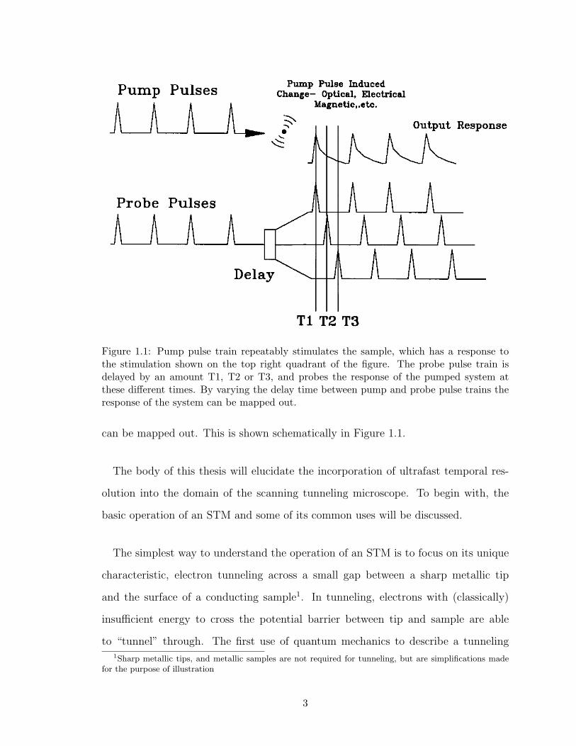
Figure 1.1: Pump pulse train repeatably stimulates the sample, which has a response tothe stimulation shown on the top right quadrant of the figure. The probe pulse train isdelayed by an amount T1, T2 or T3, and probes the response of the pumped system atthese different times. By varying the delay time between pump and probe pulse trains theresponse of the system can be mapped out.
can be mapped out. This is shown schematically in Figure 1.1.
The body of this thesis will elucidate the incorporation of ultrafast temporal res-
olution into the domain of the scanning tunneling microscope. To begin with, the
basic operation of an STM and some of its common uses will be discussed.
The simplest way to understand the operation of an STM is to focus on its unique
characteristic, electron tunneling across a small gap between a sharp metallic tip
and the surface of a conducting sample1. In tunneling, electrons with (classically)
insufficient energy to cross the potential barrier between tip and sample are able
to “tunnel” through. The first use of quantum mechanics to describe a tunneling1Sharp metallic tips, and metallic samples are not required for tunneling, but are simplifications made
for the purpose of illustration
3

phenomena was published by Fowler and Nordheim in 1928[19], as they used the
“new mechanics” in their description of field emission. Bringing a tip and sample into
close proximity will increase the probability that an electron will tunnel between the
two. Tunneling will occur in both directions but by applying a bias voltage between
tip and sample a net tunneling current can be established in the volume known as
the tunnel junction. This tunneling current has some special characteristics which
determine the properties of the scanning tunneling microscope.
• The tunneling current changes exponentially with tip/sample separation
• The current is spatially dependent on the shape of the active (tunneling) wave-
functions of tip and sample
• The rate of change of the tunneling current with respect to applied voltage is
correlated with electronic properties of the sample
The first point suggests that an STM will have excellent sensitivity to changes in
topography, as the tunneling current will change drastically for small changes in the
distance between tip and sample. In addition the exponential decay constant (effective
work function) can give information on the quality of the sample surface, since surface
impurities such as oxide layers will drastically effect the decay constant. The second
point suggests that an STM will have lateral resolution related to a convolution of
the tip and surface wavefunction. The third point implies that an STM could be used
for determining information about the local electronic properties of a sample being
studied. With these “potential” features in mind, the basic design of an STM will be
discussed.
1.1.2 A typical STM and its applications
Mechanical design is a fundamental requirement to exploit the first two properties
mentioned, and create a microscope capable of measuring topographic features on a
surface . The microscope must allow for atomically precise positioning of a sharp tip
4

above a sample of interest. This requires an approach mechanism which can bring
the tip from macroscopic separations of millimeters down to the nanometer range
separation necessary to attain a measurable tunneling current. Once separation is of
this order, there needs to be a fine control actuator capable of moving the STM tip
laterally and vertically with sub A resolution. In the present example a piezo-electric
cylindrical tube (PZT tube 2 ) will be used for this purpose. Piezo-electric materials
were discovered by Pierre and Jacques Curie in 1880 [20]. They are ferroelectric or
antiferroelectric and will change their structure when voltages are applied across them.
A piezo tube can act as a mechanical actuator with sub A precision [21]. The system
must be stabilized and isolated from environmental interference such as mechanical
vibrations and electrical noise. Mechanical vibrations cause relative motion between
tip and sample distorting the tunneling current. Similarly electrical noise will obscure
the tunneling current. The typical microscope operates with the tunneling current
between tip and sample maintained through a feedback system. The current is kept
constant by adjusting the height of the STM tip above the sample surface. The tip
is scanned over a small area on the sample surface using a computer to initiate the
scan and record the relative tip height while the feedback loop maintains constant
current. In this manner we form an image of the topography of the surface.
The control and measurement electronics are shown schematically in Figure 1.2.
Illustrated is a sample at a potential determined by the applied bias voltage. The
STM tip is positioned above the sample and mounted in a cylindrical piezo tube which
controls tip position in 3 axes (with a small amount of cross coupling between the
x-y and the z axis) as control voltages are applied through the high voltage amplifier.
Current signals from the STM tip are amplified in a current pre-amp (typical pre-
amp gain is 108 → 109V/A) and sent to the feedback controller. Changes in tunneling
current are minimized as the feedback controller is connected to the tip height (Z)2PZT is an industry name for lead, zirconate titanate, a single phase solid solution of PbZrO3 and PbTiO3
5

High Voltage Amp
Input Output
Mod YMod X Mod Z
Z connected to innersurface of Piezo
Sample
Piezo Tube
BiasPreamp
Feedback Controller
STM
+X -X +Y -Y Z
X out Y out
Scan
Controller Feedback monitor
Current Monitor
STM Tip
Figure 1.2: Basic elements of a Scanning Tunneling Microscope
6
input of the high voltage amp, allowing the STM tip to approach or withdraw from the
sample surface to maintain a constant tunneling current. While efforts to maintain a
constant tunneling current are made, the current is monitored and recorded by the
scan controller to assess the effectiveness of the feedback system. The scan controller
also monitors the output of the feedback controller as it adjusts the tip height above
the sample. When a scan is initiated by the scan controller it outputs voltages to
the high voltage amplifier directed to the x and y electrode pairs of the piezo. These
voltages cause deflection of the piezo tube allowing it to scan the tip across the sample
surface.
With a configuration such as that shown in Figure 1.2 all of the unique features
of the tunneling current can be exploited to glean information about the sample
through tunneling microscopy. The vertical resolution of the scan is related to the
effective work function of the tunnel junction. Surface impurities can assist tunneling
by lowering the effective work function, while a cleaner junction yields a higher work
function and better topographic sensitivity. The lateral resolution also varies with
work function and the electronic states of the STM tip. If electrons are tunneling into
highly localized orbitals on the STM tip, the lateral resolution will be better than
simply tunneling into an electronically uniform tip. The “electronic” shape of the tip
is a key characteristic of STM topographic scans, and much work has been done to
model and characterize STM tip shapes.
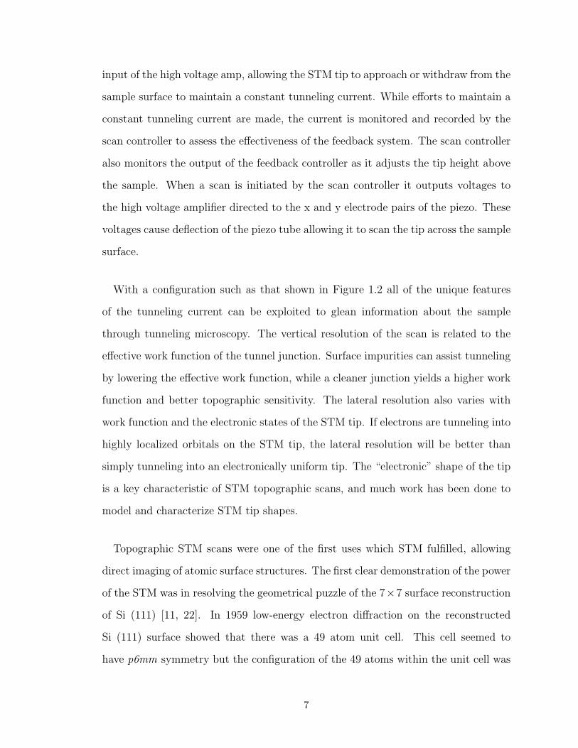
Topographic STM scans were one of the first uses which STM fulfilled, allowing
direct imaging of atomic surface structures. The first clear demonstration of the power
of the STM was in resolving the geometrical puzzle of the 7×7 surface reconstruction
of Si (111) [11, 22]. In 1959 low-energy electron diffraction on the reconstructed
Si (111) surface showed that there was a 49 atom unit cell. This cell seemed to
have p6mm symmetry but the configuration of the 49 atoms within the unit cell was
7

Figure 1.3: 7× 7 reconstruction on Si (111); panel a) shows STM topographic scan; panelb) shows calculated structure.
unknown. Many models were proposed but the exact structure remained a mystery
through 20 years of investigation until an STM directly imaged the surface. Direct
imaging revealed that all the proposed models were incorrect and the true symmetry
of the unit cell was p3ml. The first published STM reconstruction is shown in cell a)
of Figure 1.3. The reconstruction is not completely observed as 12 adatoms obscure
the full view but from the configuration of adatoms the underlying structure was
determined 3. The full 3 dimensional unit cell published in reference [22] is shown
in Figure 1.3 panel b), where the 12 top-layer adatoms form the trapezoid between
vacant centers of the surface structure.
Apart from topographic scans in constant current mode, there are other significant
modes of operating the STM. Foremost of these is current-voltage or I/V spectroscopy.
In typical STM operation, the tip height is maintained using feedback to achieve
constant current with a fixed DC bias between tip and sample. Increasing the DC
bias will raise the net current and subsequently the feedback system will withdraw the
tip reducing the current back to its original value. If however, the feedback system3Through reaction with chlorine the adatom layer can be removed and the beautiful underlying structure
imaged, see [23]
8

were disabled, the tunneling current would increase to a new equilibrium value. The
response of the tunnel junction to variations of the bias voltage can yield insight into
the electronic structure of STM tip and sample. By temporarily suspending feedback
and monitoring the tunneling current while ramping the bias voltage an I/V curve can
be acquired. It turns out (this will be shown in subsequent sections) that ∂I∂V
is directly
proportional to the density of states of the sample at the location of the STM tip. By
performing I/V scans at different points on a sample surface, a ∂I∂V
or density of states
map of the sample can be created at a particular energy. This modality of the STM
allows the creation of spectacular images such as the imaging of the local density of
states (LDOS) of NbSe2 shown in Figure 1.4. In this experiment Harald Hess imaged
the Abrikosov flux lattice of NbSe2 at 1.8 Kelvin and in a field of 1 Tesla. The lattice
is visible since the density of states for NbSe2 is suppressed within the energy gap
of the superconducting NbSe2, but reappears in the normal cores of the vortices.
This work is quite interesting in that it could be considered a continuation of work
by Binnig and Rohrer, since their original motivation for inventing the instrument
that became an STM was to develop a local electronic structure probe for studying
superconductivity.
1.1.3 STM Fundamentals
Now that some of the basic features and modalities of STM have been touched upon,
we will delve a little deeper into the quantum mechanics which found its operation.
Through this we will illustrate how the “features” of the tunnel junction can be
derived as well as how more precise calculations of tunnel junction properties can be
approached.
To understand the basic operation of a scanning tunneling microscope it is first
necessary to outline the underlying quantum mechanics. Beginning with a simple
model we will endeavor to illustrate some simple features of the phenomena of quan-
9
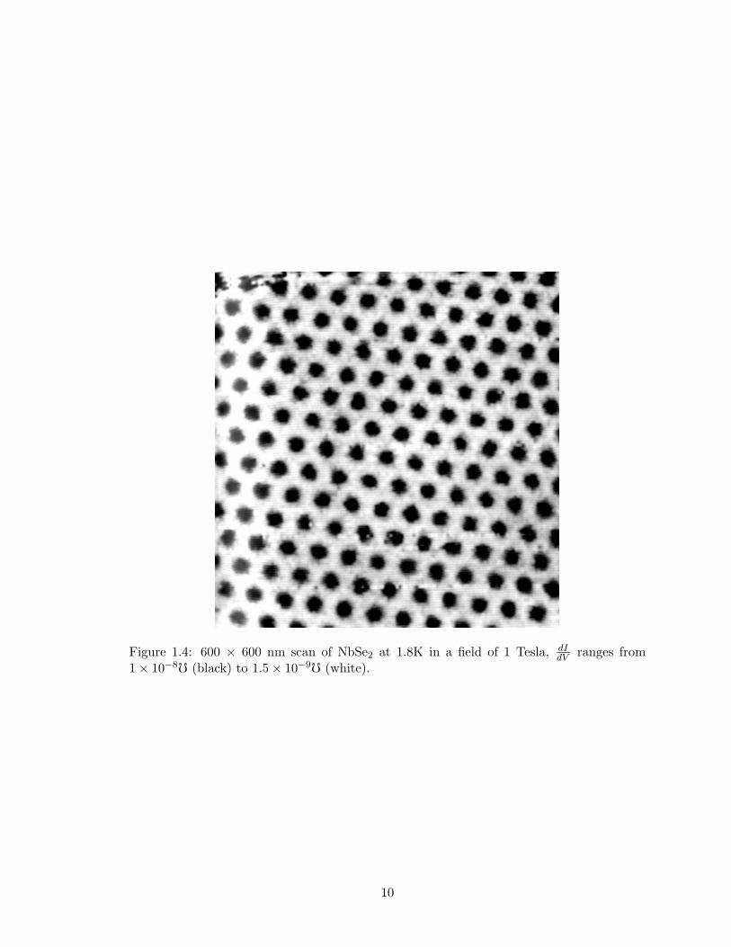
Figure 1.4: 600 × 600 nm scan of NbSe2 at 1.8K in a field of 1 Tesla, dIdV ranges from
1× 10−80 (black) to 1.5× 10−90 (white).
10

tum tunneling. As we bring the metal STM tip towards the sample, the difference in
Fermi energies between the metals is equal to the difference between their respective
work functions, shown in panel (a) of figure 1.5. As the tip and sample are brought
close enough that tunneling begins between tip and sample, an electronic equilibrium
is established as a common Fermi level between the two metals, shown in panel (b).
An electric field is also established due to the differing work functions of the two
metals. If a bias voltage is applied between STM tip and sample the Fermi levels of
each metal are shifted until their separation is equal to the bias voltage as shown in
panel (c).
A simplified tunneling barrier, shown in figure 1.6 captures the essential character
STM tunneling. Examining a free electron and a potential barrier (where the energy
of the electron E is less than that of the potential barrier V0) , we can write down
the single particle Schrodinger equation:
−h2
2m
d2
dx2ψ(x) + V (x)ψ(x) = Eψ(x) (1.1)
Solving the Schrodinger equation on the left hand side of the barrier, shown in
Figure 1.6, gives:
− h2
2m
d2
dx2ψ1(x) = Eψ1 (1.2)
ψ1 = Aeikx +Be−ikx (1.3)
where k =√
2mEh2 . Examining ψ inside the tunneling barrier where E < V0:
h2
2m
d2
dx2ψ2 = (V0 − E)ψ2 (1.4)
ψ2 = Cek′x +De−k
′x (1.5)
where k′ =√
2m(V0−E)
h2 . Finally looking at the right hand side of the tunneling barrier:
− h2
2m
d2
dx2ψ3(x) = Eψ3 (1.6)
ψ3 = Feik′′x +Ge−ik
′′x (1.7)
11

EF
EF
EFEF
EF
E vac
EF
BiasV
(c)(b)(a)
Figure 1.5: (a) Two metals well separated by a vacuum gap, the Fermi levels are separatedby the difference in work function between each metal. (b) Metals are brought close togetherand reach an electronic equilibrium where they share a common Fermi level. (c) A biasvoltage introduces a Fermi level shift between the two metals. Only electrons below theFermi level on the left can tunnel into states above the Fermi level on the right.
12

V0
ψ2
ψ3ψ1
0 a x
V(x)
Figure 1.6: Potential Barrier
where we set G = 0 for an incoming particle from the left, and where k′′ =√
2mEh2
Matching equations 1.3 and 1.5 and their first derivatives at the x = 0 boundary gives
us:
A+B = C +D (1.8)
ik(A−B) = k′(C −D) (1.9)
While matching equation 1.5 and 1.7 at the x = a boundary gives:
Feik′′a = Cek
′a +De−k′a (1.10)
ik′′Feik′′a = k′(Cek
′a −De−k′a) (1.11)
Eliminating variables C and D we can solve for the ratio’s BA
and FA
also noting that
by definition k′′ = k, we write:
B
A=
(k2 + k′2)(e2k′a − 1)
e2k′a(k + ik′)2 − (k − ik′)2(1.12)
F
A=
4ikk′e−ikaek′a
e2k′a(k + ik′)2 − (k − ik′)2(1.13)
At this point it would be possible to solve explicitly for A, B and F by normalizing
the wavefunction∫ +∞−∞ ψ∗(x)ψ(x)dx = 1, but it is more convenient to simply calculate
the reflection and transmission coefficients where the reflection coefficient is given by:
R =|B|2
|A|2=
[1 +
4E(V0 − E)
V 20 sinh2(k′a)
]−1
(1.14)
13

And the transmission coefficient is given by:
T =|F |2
|A|2=
[1 +
V 20 sinh2(k′a)
4E(V0 − E)
]−1
(1.15)
For effectively large tunneling barriers where k′a >> 1, sinh2(k′a) ≈ e2k′a
4so that T
is given by:
T ≈ 16E(V0 − E)
V 20
e−2k′a (1.16)
The value (2k′)−1 can be thought of as a characteristic range for tunneling. Choosing
a typical barrier height of (V0 − E) = 3 eV and a tip height of 3 A gives us a
value e−2k′a = 4.89 × 10⁻³. 4 From equation ( 1.16) we ascertain some essential
characteristics of the tunnel junction. The tunneling transmission probability and
hence the tunneling current will vary exponentially with tip/sample separation and
the tunneling current will also vary exponentially with the square root of the effective
tunneling barrier height (since k′ =√
2m(V0−E)
h2 ). This extreme current dependence
on tip height suggests that the STM should have excellent resolution to small changes
in sample topography. A topographic change towards or away from the surface of 1 A
can change the value of the exponential in equation 1.16 from 4.9×10⁻³ to 2.9×10⁻²
or 8.3 × 10⁻⁴ respectively, an order of magnitude change in tunneling current for a
height change of just 1 A! This exponential dependence can be seen over many orders
of magnitude as the STM tip is withdrawn from a sample surface as shown in the
early work of Binnig, Rohrer et al. [24].
In order to better explain the exact form of the tunneling current it is necessary
to develop a detailed model of STM tip and sample. Features of this model will be
the modification of tip and sample wavefunction as the two are brought into close
proximity, and the detailed electronic states of tip and sample.4Comparing this with 4 sinh2(k′a)−1 = 4.9 × 10⁻³ shows that the approximation is sufficient in a
reasonable tunneling configuration.
14

A detailed description of the theory of STM modeling can be found in chapters
2, 3 and 4 in Chen’s “Introduction to Scanning Tunneling Microscopy” [21]. In this
reference Chen details the development of the modified Bardeen approach, to model
STM tunneling current. Comparisons are made with some exactly solvable quantum
systems, and detailed approaches to calculate the tunneling matrix element are given.
The fundamental equation of interest in calculating tunneling current is derived as:
I =4πe
h
∫ +∞
−∞[f(EF − eV + ε)− f(EF + ε)] (1.17)
×ρS(EF − eV + ε)ρT (EF + ε)|M |2dε,
where f(E) = (1 + e(E−EF )
kBT )−1 is the Fermi distribution function used for both tip
and sample in the above equation. ρS is the sample density of states and ρT is the
tip density of states. M is the tunneling matrix element, which is related to the
interaction between tip and sample states. From here we can simplify equation 1.17
by substituting a step function for the Fermi distribution allowing us to write:
I =4πe
h
∫ eV
0
ρS(EF − eV + ε)ρT (EF + ε)|M |2dε. (1.18)
If we have an STM tip with a constant density of states ρT then the tunneling current
can be written as:
dI
dV∝ ρS(EF − eV ), (1.19)
where we see that the derivative of the STM tunneling current is a direct local probe
into the sample local density of states at the applied bias voltage V . Returning to
equation 1.17, the tunneling matrix M is given by:
M = − h2
2m
∫(χ∗ν∇ψµ − ψµ∇χ∗ν) • d~S, (1.20)
where ψµ is the wavefunction of the sample and χν is the wavefunction of the tip.
In determining the wave function of the tip we limit our choice to wavefunctions
extending out of the tip into the vacuum between tip and sample. Following Chen’s
15

derivation one finds that for a given tip state, there exists a matrix element operator
for the surface state.
This result, first derived by Tersoff and Hamann [25, 26] reduces the calculation
of the matrix element to the problem of simply finding the appropriate surface wave-
function.
To determine the surface wavefunction many models have been developed. These
models account for bulk Bloch wave states through the material, surface states which
would be forbidden in the bulk material as they would rest within material bandgap-
s, and surface resonant states which are surface states with overlapping bulk Bloch
states. One of the early models of the electronic structure of a metal surface is the Jel-
lium model. This model consists of a bulk Sommerfeld free-electron model where the
background ion potential drops to zero at the surface. Using this model, Bardeen [27]
estimated the work function of various metals and found fair agreement with ob-
servation (within about 25%). This model is not particularly useful as it does not
incorporate any atomic structure necessary to predict things like surface states, how-
ever this model has found use in calculating surface wavefunctions for single adatoms
on a surface as shown by Eigler et al. [28]. A model explicitly predicting the existence
of surface states was formulated in 1932 by Tamm [29], based on a Kronig-Penney po-
tential with a boundary. But the most accurate and successful calculations of surface
wave functions are first principle calculations using density-functional theory. Using
density-functional theory Appelbaum and Hamann pioneered the first calculations of
electronic surface structure examining sodium and aluminum in the early 1970’s [30].
Of course it is of great interest and use to be able to calculate surface wavefunction-
s, but STM measurements provide a simple and effective way to access this same
information, through local density of states measurements.
16

Figure 1.7: Anomalous STM images of graphite.
The origins of the STM tunneling current can now be seen. Beginning with the
equation for tunneling current, we substitute in the Fermi functions for STM tip
and sample. Then we approach the tunneling matrix element, using the appropriate
STM tip wavefunction (determined by the material and detailed shape of the STM
tip apex) and calculated surface wavefunction. The significance of both the tip and
surface wavefunction on the tunneling current belies the assumption that STM images
always convey true surface topography. Care must be taken in any interpretation of
an STM topographic scan. A dramatic example of how the tip wavefunction can affect
topographic images is shown in Figure 1.7 from work by Mizes, Park and Harrison [31].
The left image of each pair labelled a) through d) is an actual STM scan while the
right image is computer generated using a model tip geometry (since the geometry of
the tip atoms dictate the overall tip wavefunction shape). Only panel a) shows the
accurate topography of the graphite sample being studied. The images from panels
b) through d) show actual STM images of a graphite surface but because the tip of
the STM had multiple atoms involved in tunneling the images do not display the true
topography of the surface.
Now that the basic principles of STM operation have been discussed we will begin
discussion into methods to add ultra-fast time resolution to this microscopy.
17

1.2 History of Time Resolved STM
1.2.1 Initial Developments in Time-Resolved Scanning Probe Microscopy
The young field of time resolved scanning tunneling microscopy has mysterious o-
rigins. The first proposal can be traced back to a two paragraph note published
anonymously as Research Disclosure # 30480 in August 1989 in the journal Re-
search Disclosures [32]. This disclosure, entitled “Contactless, High-Speed Electronic
Sampling Probe” proposes the use of a vacuum tunneling probe to sample electrical
transients which are produced optically or electronically and rectified by the nonlin-
earities of the current-voltage characteristic of the tunnel junction. Due to the brevity
of the article it will be quoted below:
“A vacuum tunneling probe may be used for the sampling of
electrical transients.
The sampling device consists of a metal tip in close proximity to an
electrical conductor in which the transient propagates. An optical pulse
incident on this metal-vacuum-metal tunneling junction is rectified by non-
linearities in the current-voltage characteristic of the junction. The coinci-
dence of electrical and optical pulses changes the junction response, thereby
providing a cross-correlation of the pulses. By varying the delay between
the pulses, the complete cross-correlation is obtained. This vacuum tun-
neling junction is expected to have a frequency response better than 200
THz (5 fs). The contactless probe may also be laterally scanned in order
to probe different parts of the circuit. With a scan length of the order of
microns, it is possible to look for inhomogeneities and defects of individual
elements in an integrated circuit.
The sample is shown schematically in the drawing[figure not shown]. A
DC tunneling current ib produced by a DC voltage bias is used to main-
tain a constant tip-sample separation. Electrical pulses at the junction
will effectively change the bias, producing a current ie. Optical pulses will
be rectified by the nonlinearities of the junction producing a current io.
Because the nonlinear properties of the junction depend on the bias, coin-
cident optical and electrical pulses will produce an additional component
18

ioe of the total current. This component provides a measure of the cross-
correlation between electrical and optical pulses. The correlation signal ioe
may be enhanced using difference frequency lock-in techniques. We note
that even without the presence of optical pulses, this device may be used
for contactless electrical sampling with conventional electronic bandwidths
due to the current ie. We also note the possibility of using this sampler,
in conjunction with the vacuum tunneling pulse generator, to measure the
transient response of a circuit or device with subpicosecond resolution and
also as a broadband autocorrelator to measure subpicosecond laser pulse
widths.”
Due to the unusual nature of this publication, and the small audience which received
it, little was known of time resolved STM until the independent work of Hamers and
Cahill [33, 34]. The primary paper, entitled “Ultrafast time resolution in scanned
probe microscopies”, demonstrated the first attempt to combine laser methods for
ultrafast time resolution with a scanning capacitance microscope. The authors went
further though, in outlining the technique and requirements to add ultrafast time
resolution to scanning probe microscopes in general (their original motivation had
been to attempt a time-resolved detection of surface photovoltage using a scanning
tunneling probe).
The process that the authors studied was the decay of photoexcited carriers at a
Si (111) (7× 7) surface. Their experimental setup is shown in Figure 1.8.
In this scheme, they proposed that, ”Using the SXM5 probe tip as a local de-
tector of a deviation from equilibrium which is a nonlinear function of an externally
controlled stimulus (such as an optical pulse), it is possible to achieve unprecedented
time resolution which is limited only by the inherent time scale of the underlying
physical process.”
In their experiment a scanning capacitance microscope was used as the local probe,
and optical pulses from a dye laser were used to create a transient surface photo-
voltage (SPV) which was detected by the probe. Using a capacitive probe allows the5Where SXM refers to a generic scanning probe microscopy
19

Figure 1.8: Schematic diagram of experimental apparatus. ÷ N = Cavity dumper, EOM= electro-optic modulator, PP = polarizing prism, AC=autocorrelator, TP = thermopiledetector.
tip sample separation to be large minimizing the effects of photothermal expansion
or sample and tip due to laser intensity fluctuations. Under continuous illumination
the magnitude of the SPV varies as:
SPV ≈ A ln(1 + CδQ/Q) (1.21)
where A and C are constants and δQ is the photoexcited carrier density [35]. Under
pulsed illumination using 1 ps pulses every 13.1 ns the SPV can be fit with this same
equation (with modified values of A and C) as shown in Figure 1.9. The fitting curve
was generated with A=28 mV which is almost identical to the value A=31 mV found
under continuous illumination suggesting that carrier relaxation occurred on time
scales slower than 13.1 ns. To probe carrier relaxation on longer time scales a cavity
dumper was used to vary the repetition rate of laser pulses at the sample surface.
One picosecond duration excitation pulses would arrive with a spacing (in time) in
increments of τML = 13.1 ns. The authors measured the average photo-voltage as
they varied the repetition rate of their excitation pulses from τML to 40× τML while
maintaining a constant time averaged illumination intensity. In this way they could
20

Figure 1.9: Dependence of SPV on incident power using 1 ps pulses separated by 13.1 ns.
look for deviations from Equation 1.21.
When the cavity dumper repetition rate was high with respect to the carrier relax-
ation time, a large carrier density would be established producing a saturated SPV
and measured displacement current signal (through repeated pumping of the sample).
For a long repetition rate (compared to the recombination time) most photo-carriers
recombined diminishing the SPV before the next excitation pulse resulting in a di-
minished current signal. The excitation pulse train was optically chopped at 4 kHz
so that a lock-in amplifier could be used for detecting and discriminating the time
resolved signal. An averaging transient recorder measured the displacement current
induced in the tip at 4 kHz. Integrating the displacement current over the “on” time
of the chopper gave an averaged value proportional to the time-averaged SPV. A SPV
plot with respect to the pulse separation time is shown in Figure 1.10.
21
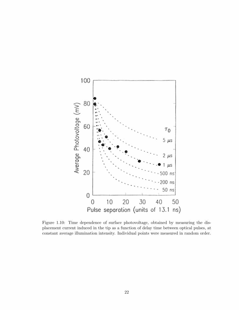
Figure 1.10: Time dependence of surface photovoltage, obtained by measuring the dis-placement current induced in the tip as a function of delay time between optical pulses, atconstant average illumination intensity. Individual points were measured in random order.
22

This curve was fit and a 1µs carrier decay time was deduced in the limit of
small photovoltages. This experiment was the first to use a scanning probe to detect
a signal with fast transient origins. The authors did not report on the effect of
scanning the detector over the silicon surface so combined spatio-temporal resolution
was not demonstrated. The technique used to achieve time-resolution in this case
relied solely on properties of the sample under investigation. The saturation of the
SPV at different pump powers and pump repetition rates allowed the authors to
deduce the carrier recombination time for the Si (111) surface, but this technique is not
generalizable for time-resolved studies of other material properties. Nonetheless the
authors demonstrated the first use of a local probe to investigate the 1µs photoexcited
carrier recombination time of a Si (111)-(7× 7) surface.
1.2.2 Time-Resolved Electrostatic Force Microscopy
Two years after the work by Hamers and Cahill, the group of Hou, Ho and Bloom
published results demonstrating picosecond time resolution using a scanning electro-
static force microscope (SFM) [36]. Atomic force microscopes (AFM) had only been
invented about 6 years earlier by Binnig, Quate and Gerber [6] and were already
acquiring a great number of industrial applications due to their flexibility and ease
of use. Adding ultrafast time resolution to a modified AFM would prove to be not
only interesting, but quite practical. In the Hou, Ho, Bloom scheme the nonlinear
force F = − ε0AV 2
2z2 between SFM tip and the sample would serve to mix the exci-
tation response of the system with a time varying probe signal. This differed from
the Hamers and Cahill experiment where they used repetitive pumping at differing
time intervals to build a measurable signal (there was only a pumping stimulus and
the frequency of this stimulus was varied). In the Hou, Ho, Bloom configuration two
different signals, a pump and a probe signal at different frequencies were mixed in
the force nonlinearity to produce a difference frequency signal within the bandwidth
of the SFM cantilever and electronics.
23

Figure 1.11: SFM electrical mixing at 1 GHz.
In demonstrating this technique the authors combined the 1 Volt outputs of two
synthesized sinusoidal signals at frequencies f and f+∆f , and launched the combined
signal down a transmission line (TRL). The fundamental frequency f=1GHz was used
and ∆f was varied from 0 → 25 kHz. The deflection amplitude of the cantilever is
shown in Figure 1.11.
The 19 kHz peak corresponds to the mechanical resonance frequency of the can-
tilever. By characterizing the mechanical resonances of the SFM tip, the mixing
signal can be obtained. Similar mixing experiments were successful up to 20 GHz,
limited by the quality of the experimenters’ high speed electronics.
This group also performed experiments in the time domain using a pair of step-
recovery-diode (SRD) comb generators, which produced 110 ps pulses at 500 MHz
and 500 MHz + 10 Hz respectively. These pulse trains were combined and launched
onto a co-planar waveguide structure patterned onto a GaAs substrate. The beat
pattern from the two pulse trains is shown in Figure 1.12, where a 130 ps correlation
24

Figure 1.12: Equivalent-time correlation trace of two 110 ps pulse trains
between pulse trains is shown.
In their concluding remarks, the authors contend that this technique should be
capable of measuring voltage signals with picosecond time resolution and submicron
lateral resolution. This technique should be quite useful especially when excitation
and probe pulses are close enough in frequency that the mechanical cantilever will
respond with sufficient amplitude to be detected. One questions the ultimate resolu-
tion of this technique as it relies on a tip sample force which is capacitive in origin,
yet the technique should provide the submicron resolution the authors suppose.
The absolute magnitude of the mixed signal is a convolution of the force exerted
on the cantilever, due to the voltage pulses being measured, and the mechanical
response of the cantilever. This complication was later addressed using a nulling
method developed by Bridges, Said and Thompson [37] in their time-resolved AFM
system. In the work by Bridges et al. the electrostatic force between a flexible
25

tip and sample is monitored and used to demodulate an ultrafast signal. The sample
under investigation is repetitively pumped and probed and by cleverly modulating the
amplitude of the repetitive probe signal while adding a variable AC dither the sample
response can be accurately mapped, irrespective of the cantilever displacement. The
force between cantilever tip and sample can be written as:
FZ = −1
2
∂
∂zC(x, y, z) [vp(t)− vc(x, y, t)]2 (1.22)
where vc is the voltage on the circuit element being tested, vp is the voltage on
the scanned probe, and C(x, y, z) is dependent on the probe tip/circuit geometry
and position. To measure vc one could use a series of probe pulses similar to the
technique of Hou et al., calibrating the response of the cantilever would still be a
problem though. The trick that Bridges, Said and Thompson used was to use a
modulated pulse train to probe the circuit voltage. The initial sampling voltage train
was given as vs(t) = Gδ(t − τ) (where Gδ(t − τ) is a step function at time τ with
width δ) but this was modified, giving vp(t) = [A + K cos(ωrt)]vs(t) where wr is the
resonant frequency of the cantilever. In the previous equation the variables A, K and
vs(t) are all user controlled parameters. Using vp(t) in equation 1.22, gives a number
of terms in the force equation. Most of these terms will appear as DC contributions
but there will be a term at the modulation frequency ωr, which a lock-in amplifier
can detect. This term is expressed as:
Fz|ω'ωr = − ∂
∂zC(x, y, z)× [A〈vs(t), vs(t)〉 − 〈vs(t), vc(x, y, t)〉]K cos(ωrt) (1.23)
where 〈a, b〉 = 1T
∫Ta(t)b(t)dt is the inner product over the period T. Using vs(t) in
equation 1.23 and evaluating the inner product 〈vs(t), vs(t)〉 noting that δ is the width
of the impulse Gδ(t− τ), we rewrite Fz as:
Fz|ω'ωr = − ∂
∂zC(x, y, z)×
[A · δ
T− 〈Gδ(t− τ), vc(x, y, t)〉
]K cos(ωrt) (1.24)
26

Under the condition that the width of the impulse approaches zero, we note that
〈Gδ(t − τ), vc(x, y, t)〉 ⇒ vc(x, y, t = τ) · δT
. Recalling that vc(x, y, t) is the function
we are trying to determine, we see that by adjusting the modulating parameter A to
null the force Fz, one can easily determine vc. This approach only works when the
response of the detection system is very slow compared to the speed of the sampling
pulses.
The work by Hou, Ho and Bloom was quite illustrative for early proposals for time-
resolving STM operation, especially the junction mixing techniques. In the Bloom
work, a pump/probe configuration was used, where pump and probe signals were
mixed in the squared voltage nonlinearity exerting a force on the AFM tip. The tech-
nique of Greg Bridges et al., employed this same nonlinearity, but by using a single
excitation source for pump and probe pulses, the electronics required were greatly
simplified. The nulling procedure overcomes the problems of calibrating cantilever
response and allows the determination of the response of a sample to electrical exci-
tation. These techniques offer fast time resolution, demonstrated into the picosecond
range, but the spatial resolution of this technique will be limited by the range of
the geometrical capacitance between tip and sample. For time-resolved microscopies
where atomic scale spatial resolution is necessary one must look past other scanning
probe microscopes to the grandfather of the field, the STM.
1.2.3 Time-Resolved Scanning Tunneling Microscopy
1993 was a banner year for experiments demonstrating the time-resolved operation
of the scanning tunneling microscope. Four papers, published over a two month span
by three different groups, brought three competing methods to add ultrafast time
resolution to STM operation. These papers were published virtually simultaneously,
but they will be introduced chronologically for consistency.
27

The first of the four introduced the technique of photo-gated or PG-STM [38]. In
PG-STM an optical pulse train was split into a pump/probe configuration, the pump
beam repetitively stimulated the sample under investigation while the probe beam
was directed to an optical switch embedded in series with the tip of the STM. Because
the switch has a finite “dark” resistance of 30MΩ (small compared to a typical STM
tunnel junction resistance of 100MΩ or more) the STM can still operate without
illuminating the switch. The idea with this configuration is to use the pump beam to
stimulate the sample such that the tunneling current between tip and sample will be
modified when the sample is being pumped. Without the probe beam the additional
current will be small, the electronics of the STM will integrate this additional current
contribution and the feedback system of the STM will compensate by adjusting the
STM tip height. When the probe is implemented, the current contribution from
coincidence between pump excitation and probe gating will be enhanced. Under
these circumstances, the STM electronics will again integrate the excess current and
the STM feedback electronics will adjust the tip height accordingly. To avoid this,
the pump and probe beams are optically chopped at different frequencies, where the
chopped frequencies are outside the response time of the feedback system, but within
the bandwidth of the STM current pre-amp. A lock-in amplifier is used to detect the
excess current at the chopping sum or difference frequency (beating). By shifting the
phase between pump and probe pulse trains, a cross-correlation between the response
of the sample (to the pump pulse), and the response of the photo-conducting switch
(to the probe pulse), can be created. If one characterizes the response of the photo-
conductive switch, the response of the sample can be extracted by deconvolution. The
experimental setup used by Weiss et al. is shown in Figure 1.13. The cross-correlated
current measured by this device is shown in Figures 1.14 and 1.15. In Figure 1.14
each trace is at a different tunneling resistance. Figure 1.15 shows the time-resolved
current measured through tunneling and across a tip in contact with the transmission
line. In their results Weiss et al. noted that the time resolved signal is proportional
28

Figure 1.13: Ultrafast STM. One laser pulse excites a voltage pulse on a transmission line.The second pulse photoconductively samples the tunneling current on the tip assembly.
29

Figure 1.14: The tunneling current ∆I(∆t) for different gap resistances (16, 32, 128, and256 MΩ from top to bottom).
30

Figure 1.15: Time-resolved current cross-correlation detected on the tip assembly, (a) intunneling (5 nA and 80 mV settings), (b) when the tip is crashed into the sample, and (c)is the time derivative of (b).
31

to the average tunnel currents, from which they concluded that there is no geometrical
capacitive contribution to the time resolved signal. By extracting the tunneling tip
50 A from the surface, the DC and time-resolved currents drop to zero. The authors
used this evidence to conclude that the PG-STM technique has spatial resolution of
at least 50 A. This conclusion is not valid. Even in ordinary STM I/Z sensitivity and
lateral resolution are essentially unrelated. Another interesting observation was that
the time-resolved correlation pulse width increases with increasing gap resistance.
This the authors attribute to an RC time for the tunnel junction, where R is the
gap resistance and C is a quantum capacitance between tip and sample. In the
conclusion of this publication the authors included a (0.7 × 0.7 µm2) topographic
scan of their transmission line. They contest that this spatial scan represents a frame
in a time-resolved movie; this is not the case as contrast in the image contains no
time-dependence.
The Weiss et al. interpretation of these experiments was not satisfying. One
perplexing question was the role of tip/sample geometrical capacitance. According to
Weiss et al., a quantum tip/sample capacitance (≈ 10−18F) played a significant role
in the shape of the time-resolved current. This was supported by the evidence that
the shape of the time-resolved signal changes dramatically if the STM tip is crashed
into the sample (transmission line) as shown in Figure 1.15. The time resolved signal
in contact looked like the integral of the tunneling signal. If a quantum capacitance
were the only source of the time resolved signal then the geometrical tip/sample
capacitance, in parallel with the quantum capacitance and 3 orders of magnitude
bigger was not having any contribution.
The true nature of capacitance in PG-STM was not resolved until 1996 by Groen-
eveld and van Kempen [39]. In their paper, “The capacitive origin of the picosecond
electrical transients detected by a photoconductively gated scanning tunneling mi-
32

croscope” the authors established that PG-STM was a capacitive microscope limited
to µm scale spatial resolution. In the Groeneveld and van Kempen model, a simple
circuit model is used where the tunnel junction is represented by a linear conductance
γ in parallel with the geometrical capacitance Ct. This tunnel junction is in series
with the photoconductive switch with time dependent conductance gs(t) in parallel
with the switch capacitance Cs. This configuration is shown in Figure 1.16. The time
dependent switch conductance and bias voltage Vin(t) are periodic with period T (10
ns), an essential feature since RC times of the tip/sample (eg. 10 Mω × 1 fF=10ns)
are comparable to the period. From this model the time-dependent tip voltage on
the tip of the STM (before the switch) is given by:
CpdV
dt+ [gs(t) + γ]V = Ct
dVin(t)
dt+ γVin(t), (1.25)
where Cp = Cs +Ct. Integrating the product of V(t) with gs(t) over the period T we
get the averaged current:
Ic =1
T
∫ T
0
gs(τ)V (τ)dτ. (1.26)
If the STM tip is withdrawn from the sample surface and γ drops to zero, then the
integrated current becomes zero since no net current can flow through a capacitor.
This explains one of the strange results of the Weiss publication. Solving equation-
s 1.25 and 1.26 for an STM tip tunneling and in contact with a transmission line
also fits the Weiss et al. result as shown in Figure 1.17.
The excellent agreement between the Groeneveld and van Kempen model and the
Weiss et al. results confirmed that the PG-STM technique would not maintain STM
spatial resolution in its application. PG-STM used the electronics of a scanning
tunneling microscope to detect a time-resolved signal which was capacitive in origin.
The ultimate spatial resolution of PG-STM is limited by the spatial extent of the
geometrical capacitance of the tip, on the order of µm’s. Another technique must be
employed if ultra-fast temporal and atomic spatial resolution are demanded.
33

Figure 1.16: Photoconductively gated STM tip above a coplanar stripline and its equivalentcircuit model shown below.
34
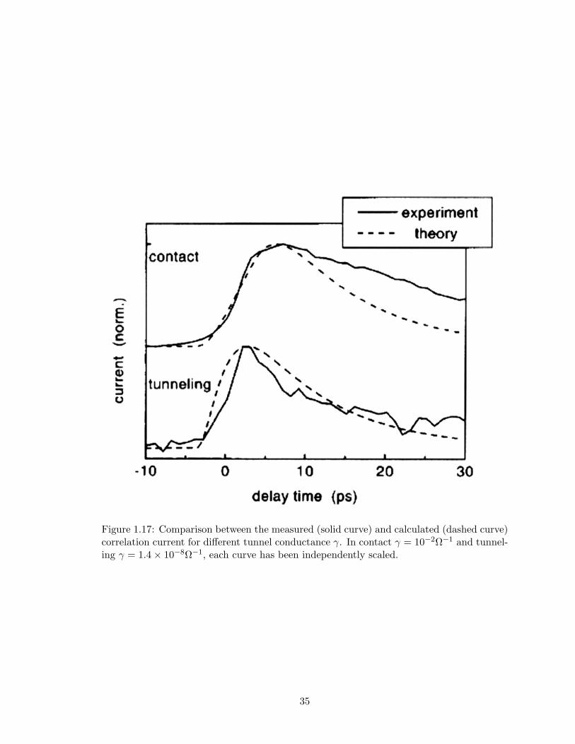
Figure 1.17: Comparison between the measured (solid curve) and calculated (dashed curve)correlation current for different tunnel conductance γ. In contact γ = 10−2Ω−1 and tunnel-ing γ = 1.4× 10⁻⁸Ω−1, each curve has been independently scaled.
35

One week after the results of the photo-gated STM technique were published (also in
Appl. Phys. Lett.), Freeman and Nunes [40] reported a completely different technique
for time-resolving an STM, the distance modulation technique. In this work a sample
is repetitively stimulated while the distance between tip and sample is varied on
a nanosecond time scale. Recall that STM tunneling current varies exponentially
with tip/sample separation. Varying this separation on a short time scale allows
the gating (or fast sampling) of a signal. This is a technique to mechanically switch
the tunneling conductance of the STM without the inherent capacitance problems
associated with having an electrical switch on the STM tip. The experimental setup
is shown in Figure 1.18 where the STM tip was electro-chemically etched nickel wire
(125 µm diameter). Nickel is magnetostrictive, changing its structure by constricting
or elongating with applied magnetic field. A pulsed magnetic field can cause an
acoustic pulse to be launched along the magnetostrictive nickel tip, modulating STM
tip/sample separation on nanosecond time scales. When biased to the steepest part of
its magnetization curve the maximum reversible magnetostriction was ≈ 0.1 ppm/Oe.
Using a static bias field of 30 Oe and applying a 80 ns, 20 Oe pulse resulted in a
maximum absolute tip displacement of 5 A (measured through time-resolved fiber-
optic interferometry). The direction of tip deflection can be changed by reversing the
polarity of the field pulse. For the experiment described, the effective tunneling work
function φ=0.45 eV gives a characteristic tunneling range (2k′)−1=1.45Awhich is less
than the 5A displacement of the tip, indicating that the acoustic pulse will have a
very significant effect on the tunneling current signal over its duration.
Using the distance modulation technique to sample an electrical pulse sent down a
gold transmission line, as shown in Figure 1.18 gives the curves shown below in Fig-
ure 1.19 6. The fact that the Time-Resolved signal reversed polarity as the pulse field
polarity was reversed illustrated the fact that the time-resolved current contribution6Note that the figure reference of Fig. 2 has not been included in this work – Fig. 2, shows an I/Z curve
and the Tip Extension time profile for the nickel tip
36

Figure 1.18: A schematic diagram of the apparatus which illustrates how the tip is threadedthrough a local magnetic field coil and the arrangement of the pulsers. Pulser 1 deliverscurrent pulses to the field coil, and pulser 2 applies voltage pulses to the gold striplinesample. The resistive (50 Ω) terminations eliminate electronic reflections.
37

Figure 1.19: Measured time-resolved tunneling current obtained using the tunnel distancemodulation technique to sample the presence of a voltage pulse on the transmission linesample. Data are shown for both directions of current flow through the magnetic field pulsecoil, and are compared with a model calculation based on the data of Fig. 2 of Ref [40].Note that the vertical scale for the lower curve has been expanded by a factor of 5. DCtunneling parameters used to stabilize the quiescent tip position are 1 nA, 50 mV.
38

decreases as the tip is withdrawn. It does not represent a negative current, just a
lowering of current relative to the average since the y-axis zero corresponds to a DC
current of 1 nA. This apparent bipolar signal is evidence that tip magnetostriction is
responsible for the time-resolved current observed. This technique is quite general in
its applications. It poses few restrictions on the type of samples which can be studied.
So long as the samples can be stimulated repetitively in a way that the STM can de-
tect, distance modulated STM can be used. The primary hindrance of the technique
is the inertia of the tip (limiting distance modulated STM to the nanosecond time
domain). A technique with “no moving parts” would enable superior time-resolution.
Motivated by this criterion the junction mixing technique was developed.
Details of the junction mixing (JM) STM technique were published less than two
weeks after the PG-STM paper [41] (3 time-resolved STM publications in 11 days!).
This approach looks remarkably similar to PG-STM but its differences are very sig-
nificant. In junction mixing the non-linearity of the STM tunnel junction is used
to demodulate ultra-fast excitations, as was proposed in the 1989 anonymous disclo-
sure [32]. In this technique a sample is repetitively stimulated (or pumped) where
this stimulus will, in some way, affect the tunneling current of the STM. The effect
could be to change the tunneling I/V characteristic, through some local surface mod-
ification, or to change the bias voltage within the original I/V characteristic. I/V
characteristics for metal insulator metal tunneling are typically given by a form of
the Simmons equation [42]:
I = β(V + γV 3) +O(V 5), (1.27)
showing a cubic non-linearity. The probe pulse, in the junction mixing technique
is launched either from the tip or the sample towards the tunnel junction, mixing
with the pump pulse at the junction itself. This leads to a time-resolved current
contribution which varies with the time delay between pump and probe pulses as
they arrive at the tunnel junction. This was demonstrated by Nunes and Freeman
39

Figure 1.20: Experimental layout for JM-STM.
in their Science paper. The experimental setup is shown in Figure 1.20. In order
to distinguish the time-resolved current contribution, an optical chopper was used
to chop pump and probe beams at different frequencies and a lock-in amplifier was
used to detect at the sum frequency. As a proof of principle experiment, photo-
conductively generated optical pulses were sent down a transmission line, with one
pulse acting as pump and one as probe. A variable delay between pump and probe was
the result of an optical delay line. When these electrical pulses arrived simultaneously
at the tunnel junction of the STM, the sum voltage leads to a non-linear increase in
tunneling current which can be seen in Figure 1.21. Because the mixing between
pump and probe pulse is occurring in the tunnel junction, this technique should
40

Figure 1.21: JM-STM time-resolved current.
41

maintain the spatial resolution of STM. This method is non-contact and essentially
non-perturbative, considering that the current leaking from the circuit under test
is on the order of pA. There are limitations to the junction mixing technique; for
the signal to “mix” in the tunnel junction the stimulated sample must offer I/V
contrast with the unstimulated sample. This might not be the case if the stimulated
sample undergoes a structural phase change which one wants to resolve, for example.
This technique offers considerable speed advantages over the distance modulation
technique and should be comparable to PG-STM in terms of speed while outstripping
PG-STM with atomic spatial resolution. Since the time-resolved signal in JM-STM
is produced at the STM tunnel junction there is no reason to suspect that the spatial
resolution of this technique will not be identical to that of an ordinary STM (the
same should be true of the distance modulation technique).
The last of the pioneering TR-STM papers was published on December 27, 1993,
two months later than the previously reported experiments. This work by Takeuchi
and Kasahara [43] seems to have been developed independently of any of the other
previous works. It seems clear the authors only became aware of the work of Hou et
al. and Weiss et al. during the course of publication. Regardless, they developed a
photo-gated STM technique and used it to show better than 300 ps time resolution.
The photo-gated technique of Takeuchi and Kasahara also falls victim to the analysis
of Groeneveld and van Kempen as a capacitive microscopy without STM spatial
resolution. The experimental setup is shown in Figure 1.22.
The sample ( a gold transmission line) is stimulated by the pulsed output of a
Schottky barrier diode, driven by a 100 MHz synthesized sinusoid. A Pt/Ir STM tip
is attached to a photo-conductive switch of Au/Mo patterned onto a semi-insulating
InP substrate. The dark resistance of the switch is around 1 MΩ, less than a typical
tunneling resistance, so the STM can operate with the photoconductive switch closed.
By illuminating the switch with 80 ps pulses (400 µW (average power) at 670nm) at
42

Figure 1.22: Schematic of probe tip and sample device, SBD is Schottky barrier diode andMSL is metal stripline.
a 100 MHz + 1 kHz repetition rate from a driven laser diode, additional current from
the STM can be gated into the STM electronics, through the 1 kΩ open resistance of
the InP switch. The pump frequency of the sample was set to be 100 MHz, so that
the probe beam would sweep across the period of the stimulated sample in 100,000
cycles. This brought the dynamics of the sample within the bandwidth of the STM
electronics, as shown in Figure 1.23. Implementation of this technique relies on an
electrical synthesizer to pump the sample and gate the STM tip current using a photo-
conductive switch stimulated by a driven laser diode. The speed of the synthesizer will
limit the time resolution of this technique. It would be advantageous to instead rely
on all optical methods for generating electrical pulses needed to stimulate the sample
under investigation. This technique is essentially a modification of the Weiss et al.
photo-gated STM technique as a photo-conductive switch mounted on the STM tip
is used to gate the STM tunneling current. This implies that the Takeuchi, Kasahara
method for time-resolving an STM will not maintain STM spatial resolution.
43

Figure 1.23: Output of the Schottky barrier diode as measured using a high-speed oscillo-scope.
44

This concludes the introduction to STM and to early developmental work on time-
resolved scanning probe microscopy. STM is capable of imaging surface topography
and sample local density of states with atomic spatial resolution. Through current-
distance and current-voltage spectroscopies the STM is capable of characterizing ad-
ditional material properties. Conventional STM images are essentially static, as STM
control electronics are limited to kHz bandwidths. In order to time-resolve the opera-
tions of a scanning tunneling microscope various pump/probe schemes were explored.
The three most prominent of these are photo-gated STM, distance modulated STM
and junction-mixing STM. Photo-gated STM has been demonstrated to have 2 ps
temporal resolution and 50 A vertical resolution limited only by the apparatus used
in these early experiments. Photo-gated STM does not achieve STM spatial resolu-
tion, as shown by Groeneveld and van Kempen [39]. Distance modulated STM has
been shown to have nanosecond time resolution as well as A vertical resolution. The
mechanical response of the magnetostrictive tip should ultimately limit the time res-
olution of this technique. There is no reason to suspect that the distance modulation
technique will not achieve the same atomic spatial resolution as an ordinary STM.
Junction mixing STM, like photo-gated STM was shown to have picosecond time
resolution (130 ps) and A vertical resolution. Since the junction mixing technique
mixes pump and probe excitations at the tunnel junction of the STM this technique
should also maintain atomic spatial resolution.
The junction mixing technique presented above is the most promising technique for
adding ultrafast time resolution to the STM. A JM-STM is an electrical demodulation
technique without moving parts, expected to outperform the method of distance
modulation. In junction mixing, the tunnel junction of the STM should give rise to
the time-resolved signal. No spatial resolution should be lost, as in the capacitively
coupled signal measured using PG-STM. Though JM-STM seems the best candidate
45

for time-resolved STM further experiments were required to prove it.
References
[1] G. Binnig and H. Rohrer. Helv. Phys. Acta., 55:726, 1982.
[2] G. Binnig and H. Rohrer. Rev. Mod. Phys., 56:615, 1987.
[3] G. Binnig and H. Rohrer. Surface Science, 126:236, 1983.
[4] G. Binnig and H. Rohrer. Scientific American, August:3, 1985.
[5] G. Binnig and H. Rohrer. IBM J. Res. Develop., 30:355, 1986.
[6] G. Binnig, C. F. Quate, and Ch. Gerber. Phys. Rev. Lett., 56:930, 1986.
[7] A. Selloni, P. Carnevali, E. Tosatti, and C. D. Chen. Phys. Rev. B, 31:2602,
1985.
[8] J. A. Stroscio, R. M. Feenstra, and A. P. Fein. Phys. Rev. Lett., 57:2579, 1986.
[9] J. A. Stroscio, R. M. Feenstra, and A. P. Fein. J. Vac. Sci. Technol., A5:838,
1987.
[10] R. M. Feenstra, J. A. Stroscio, and A. P. Fein. Surface Science, 181:295, 1987.
[11] G. Binnig, H. Rohrer, Ch. Gerber, and E. Weibel. Phys. Rev. Lett., 50:120, 1983.
[12] R. A. Wolkow and Ph. Avouris. Phys. Rev. Lett., 60:1049, 1988.
[13] Zheng Gai, Yi He, Hongbin Yu, and W. S. Yang. Phys. Rev. B, 53:1042, 1996.
[14] H. F. Hess, R. B. Robinson, R. C. Dynes, J. M. Valles, Jr., and J. V. Waszczak.
Phys. Rev. Lett., 62:214, 1989.
[15] S. H. Pan, E. W. Hudson, K. M. Lang, H. Eisaki, S. Uchida, and J. C. Davis.
Nature, 403:746, 2000.
46

[16] E. Ruska. Z. Phys., 87:580, 1934.
[17] A. Prebus and J. Hillier. Can. J. Res., A17:49, 1939.
[18] D. M. Eigler and E. K. Schweizer. Nature, 344:524, 1990.
[19] R. H. Fowler and L. Nordheim. Proc. R. Soc. London, A119:173, 1928.
[20] J. Curie and P. Curie. Comptes Rendus, 91:383, 1880.
[21] C. Julian Chen. Introduction to Scanning Tunneling Microscopy. Oxford, New
York, 1993.
[22] K. Takayanagi, Y. Tanishiro, S. Takahashi, and M. Takahashi. Surface Sci.,
164:367, 1985.
[23] J. J. Boland. Surf. Sci., 244:1, 1991.
[24] G. Binnig, H. Rohrer, Ch. Gerber, and E. Weibel. Appl. Phys. Lett, 40:178, 1982.
[25] J. Tersoff and D. R. Hamann. Phys. Rev. Lett., 50:1998, 1983.
[26] J. Tersoff and D. R. Hamann. Phys. Rev. B, 31:805, 1985.
[27] J. Bardeen. Phys. Rev., 49:653, 1936.
[28] D. M. Eigler, P. S. Weiss, E. K. Schweizer, and N. D. Lang. Phys. Rev. Lett.,
66:1189, 1991.
[29] I. Tamm. Phys. Z. Sowjetunion, 1:733, 1932.
[30] J. A. Appelbaum and D. R. Hamann. Rev. Mod. Phys., 48:479, 1976.
[31] H. A. Mizes, Sang il Park, and W. A. Harrison. Phys. Rev. B, 36:4491, 1987.
[32] anonymous. Research Disclosure, August:# 30480, 1989.
[33] R. J. Hamers and David G. Cahill. Appl. Phys. Lett., 57:2031, 1990.
47

[34] R. J. Hamers and David G. Cahill. J. Vac. Sci. Technol. B, 9(2):514, 1991.
[35] R. Hamers and K. Markert. Phys. Rev. Lett., 64:1051, 1990.
[36] A. S. Hou, F. Ho, and D. M. Bloom. Electron. Lett., 28:2302, 1992.
[37] G. E. Bridges, R. A. Said, and D. J. Thompson. Electron. Lett., 29:1448, 1993.
[38] S. Weiss, D. F. Ogletree, D. Botkin, M. Salmeron, and D. S. Chemla. Appl.
Phys. Lett., 63:2567, 1993.
[39] R.H.M. Groeneveld and H. van Kempen. Appl. Phys. Lett., 69:2294, 1996.
[40] M. R. Freeman and Geoff Nunes, Jr. Appl. Phys. Lett., 63:2633, 1993.
[41] Geoff Nunes, Jr. and M. R. Freeman. Science, 262:1029, 1993.
[42] J. G. Simmons. J. Appl. Phys., 34:238, 1963.
[43] K. Takeuchi and Y. Kasahara. Appl. Phys. Lett., 63:3548, 1993.
48

Chapter 2
Advances in picosecond scanningtunneling microscopy via junctionmixing
2.1 Context
In early 1996 four groups were attempting to demonstrate time-resolved STM ex-
periments. Using photo-gated STM there was the group of Weiss et al. [1] and the
Groeneveld, van Kempen et al. group [2]. Both Freeman and Nunes, having demon-
strated the distance modulation technique [3], were inclined to abandon it in pursuit
of the faster electrical junction mixing alternative [4]. For the work developed in this
thesis the photo-gated STM technique was not pursued as it was clear the effect of
tip/sample capacitance should dominate the time-resolved signal. In the junction
mixing technique there is no where for charge to accumulate so it was suspected that
junction mixing would be immune to capacitive artifacts.
The work presented here was stimulated by the desire to improve and develop the
junction mixing technique into a proven method for acquiring ultrafast time-resolution
with an STM while maintaining STM spatial resolution. Initial experiments were de-
signed to repeat and improve on the experiments of Nunes and Freeman [4]. The first
experiment set out to tunnel into a transmission line structure while launching two
electrical pulses towards the STM tunnel junction. The pulses would be launched
49

from photo-conductive “Auston” switches [5]. By using an ion implanted GaAs sub-
strate similar to ones studied by Elezzabi et al. [6], time-resolution could be improved
over earlier work. Looking for a time-resolved signal both in tunneling range and out
of tunneling range was another test designed to show that the time-resolved signal
was not merely capacitive in origin.
Another significant aspect of the proposed experiment was that pulses could be
launched from the same side or the opposite sides of the STM tip. In previous
junction mixing experiments both pulses were launched towards the tip from the
same direction. This did not rule out the possibility that a non-linear interaction
could mix the pulses before they reached the tunnel junction, effectively eliminating
any spatial dependence on the time-resolved signal. By launching electrical pulses
from opposite sides of the transmission line towards the tip, no pulse interactions
are possible before the pulses reach the tunnel junction implying that any non-linear
mixing must occur at the tunnel junction.
2.2 Experimental Details
Details of the equipment necessary to perform time-resolved STM experiments will
now be disclosed. A working room temperature STM had been constructed by David
Fortin [7] and it provided enough optical access that time-resolved experiments could
be considered. The microscope consisted of a nano-scope STM head shell, which
incorporated the STM tip mounted on a piezo tube which had been sectioned into 4
outer quadrants and an inner surface.
The piezo tubes used were from Staveley Sensors Inc.1. The material was EBL#2(PZT-
5A) coated with gold or nickel electrodes. The piezoelectric coefficients 2 of this ma-
terial are:1contact Paul Stokes (860)291-25372the ratio of the strain component over a component of applied electric field
50

d31 A/V @ 293 K = -1.73
d31 A/V @ 4.2 K = -0.31
Young’s modulus 1010 N/m2 = 6.3
Mechanical Q = 100
For a voltage applied to the inner conductor: ∆LV
= d31Lt
and for equal and opposite
voltages applied to opposite outer quadrants:∆LV
= 0.9d31L2
dmtwhere dm = OD+ID
2is
the mean diameter of the tube, L is the length of the tube and t = OD−ID2
is the
wall thickness of the tube. Typical scan tubes have an OD=0.250”, t=0.020” and
L=1.000” giving a lateral displacement of 34 nm/V and a longitudinal displacement
of 8.7 nm/V (at room temperature). To make electrical contact to the piezo elec-
trodes use Indium Flux #3 and Indium solder #2. Use a soldering iron at 450 F,
do not overheat the piezo as it will de-pole(to re-pole a piezo follow the procedure
of Russell Petrucci from Staveley Sensors outlined on page 235 in Ref. [8]). At room
temperature it is easy to calibrate a piezo tube using the Fabry Perot interferometer,
but at low temperatures this is not always easy or possible. In this case, C. Julian
Chen devised a method for in situ piezo calibration(pages 229-233 in Ref. [8]).
The head-shell was mounted vertically, resting on 3 support screws. The tunneling
sample was mounted face up, between the 3 screws, such that the tip of the STM
would be lowered down onto the sample. The 3 screws allowed course positioning of
the STM tip and one screw could also be rotated using a stepper motor, allowing one
side of the head-shell to be raised or lowered about 800 nm per half step of the motor.
As the head-shell was being tilted the STM tip moved in increments of only 8 nm per
half step(due to mechanical reduction caused by mounting the STM tip close to the
tilting axis of the head-shell). The STM tip assembly is shown in Fig 2.1. The whole
assembly, including head-shell and mounting support was itself mounted on two heavy
metal plates suspended by springs as shown in Fig 2.2. Eddy current damping was
also employed to dampen oscillations of the mounting plates the STM rests on. The
51

Figure 2.1: STM head-shell, tip and support screws.(Hand drawn by David Fortin)
52
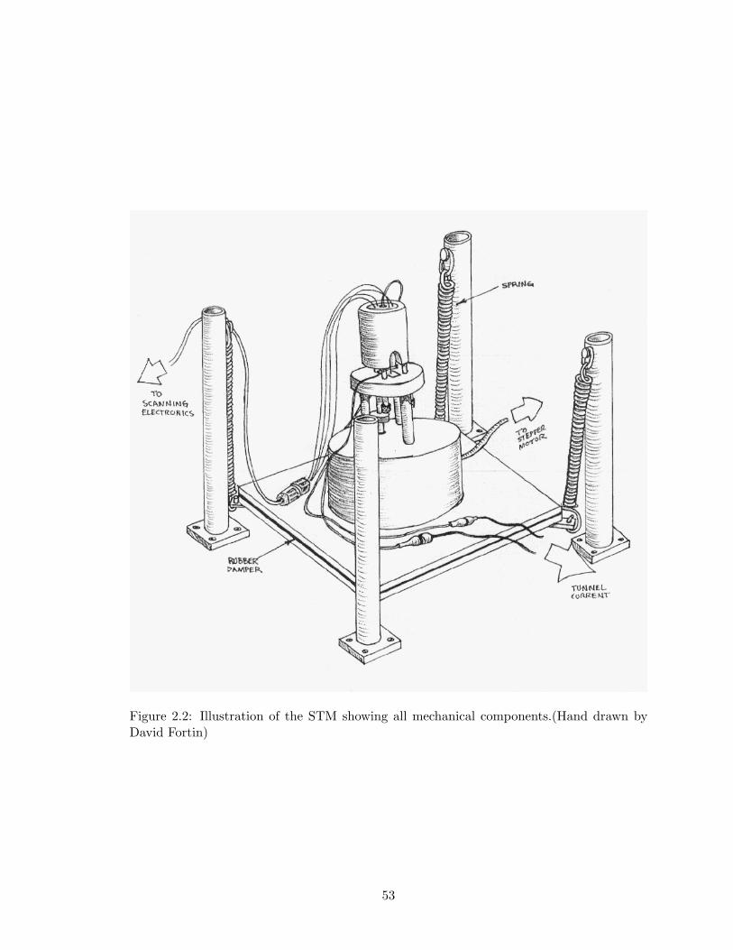
Figure 2.2: Illustration of the STM showing all mechanical components.(Hand drawn byDavid Fortin)
53
microscope was placed in a metal enclosure with Sonex acoustic damping foam panels
lining its interior3. The enclosure was mounted on a pneumatically supported optics
table in order to minimize seismic vibrations. The principle behind this vibration
isolation system is to eliminate all but the lowest frequencies reaching the working
part of the STM(the tunnel junction). The head-shell of the STM and the sample
mount are designed with high resonance frequencies so that low frequency oscillations
will drive the tip and sample together minimizing their relative motion.
The STM electronics were composed of an Ithaco 1211 current pre-amp, an IBM
CSS-D1760 analogue feedback controller and bias current supply and an IBM CSS-
F4812 high voltage amplifier. The current pre-amp, bias voltage and piezo’s are
hooked up to the electronics as shown in Fig. 2.3. For the 0.5 nA tunneling current
set point, the Ithaco pre-amp should be set on a gain of 108 V/A and the IBM
feedback controller set point should be 4.24. Feedback time constants of 1 × 1000
were typical as was a bias voltage of 50 mV. With this equipment it is also possible
to perform I/V and I/Z scans but it is necessary to connect a co-ax at 5 V to two
locations on the CSS-D1760. The first location is the Feedback/-Hold input on the
feedback control section of the CSS-D1760. The second location is the Bias/-Ramp
input on the bias voltage section of the CSS-D1760. When an I/V or I/Z scan is
initiated this 5 V line must go low, to 0 V to suspend the feedback mechanism. This
5 V line also controls the bias voltage, switching one of the bias outputs(2nd BNC
from the right) from an internal source to a ramp source(3rd BNC from the right)
for I/V scans. If one is performing I/Z scans it is important that the bias voltage is
connected to the right most BNC, to avoid any fluctuations in bias voltage.
The junction mixing STM technique relies on repetitive stimulation of the tunnel
junction by pump and probe excitations. These excitations can come from electrical
sources such as current pulsers, but for excitations in the picosecond to femtosecond3contact Illbruck inc. (517)548-6700
54

Figure 2.3: Connection diagram for the IBM feedback electronics and HV supply.
55

time scales, pulsed laser systems are typically used. At the time of these experiments
the laser system available was an Nd doped YAG system pumping a dye laser, pro-
ducing 2.8 ps pulses at 610 nm. The dye beam was split in order to create pump and
probe beams. The pump beam was focused into a single mode fiber in order to bring
the pulses into the STM chamber(metal enclosure with Sonex lined interior). The
probe beam was first sent through an optical delay line after which it was directed
into another fiber and into the STM chamber. Dispersion was not significant for these
pulses as 2.8 ps resolution was attained with this setup in a later experiment.
The initial junction mixing experiments which were published and appear later in
this chapter were electrical mixing experiments. In these experiments, two electrical
pulses were optically generated and traveled down a transmission line to the tunnel
junction of the STM(the STM was tunneling into the transmission line). In order to
create these electrical pulses suitable transmission line structures had to be created
through optical lithography. A mask was created and used to pattern a gold transmis-
sion line structure onto an ion implanted GaAs substrate. The masks were generated
using LEDIT and printed on transparencies by Screaming Colour Press4(at 3600 dpi
resolution). Semi-insulating GaAs wafers(current supplier - Sumitomo Canada Lim-
ited5), polished on one side were sent to IICO Customized Wafer Services6 for ion
implantation. They were implanted at various doses(H+ implanted at 200 keV, 7o
tilt, and implant doses 0.5, 1.63, 2.75, 3.88 and 5 ×1015cm−2). The implant is done
to produce recombination centers in the material [9]. These recombination centers
add additional energy states within the GaAs band gap allowing a faster carrier/hole
recombination than would normally occur in unimplanted GaAs(for really fast re-
combinations, use low temperature grown GaAs). Ion implants age quickly! Over
the course of months carrier recombination times grow much longer(from a few ps4phone (780)486-33005phone (416)860-38466phone (408)727-2547, note: last time they broke 2 of our substrates and did not compensate us
56

to 10’s and 100’s of ps). To reduce aging store in a cold place like a liquid nitrogen
dewar). Once the GaAs had been ion implanted, it was cleaned in an HCl dip and
then a 200 A layer of chromium and a 1000 A layer of gold were sputtered onto its
surface. Photoresist was spun onto the gold surface and then cured. After this we
used the UV lithography facility on the 6th floor to expose the resist. The exposed
resist was dissolved away and the sample was placed in both gold and then chromium
etchants. Once the GaAs substrate had been prepared it was cleaved into samples.
Each sample was mounted on a copper coated PC board. The copper provided a
ground for the transmission line structure. Contacts were made on the PC board and
wire bonds were made between the gold transmission lines and the external contacts.
BNC connectors were connected to the PC board contact pads to connect the sample
to external electronics. The characteristic impedance of this stripline transmission
line structure was calculated to be 68 Ω from page 326 of “Transmission lines for
digital and communication networks” [10].
2.2.1 Anomalous Signal
During the course of these experiments we encountered one unexpected result which
might be worth following up on. On one occasion a time-resolved signal was repeat-
ably detected after moving the tip out of the tunneling regime shown in Figure 2.4.
The experimental setup for the time-resolved experiment is shown in Figure 2.5 with
the STM tip out of tunneling range at position (B) as shown in Figure 2.5. It was
suggested that the non-contact signal was radiative in origin, coming from the photo-
conductive switches as they were illuminated. If this were the origin, then one would
expect the radiative signal would be present at the tip regardless of the relative
pump/probe timing. To detect a time-resolved signal there must be some non-linear
pump/probe interaction and the location for this interaction would probably be the
photo-conductive switches. Exploring this possibility we consider that a pulse is gen-
erated at switch (1) travels to switch (2) as the second optical pulse arrives and
57

Time Resolved Signal - in and out of tunneling range
0
0.5
1
1.5
2
2.5
3
0 50 100 150 200 250
Delay Time(ps)
Xco
mp
on
ent
-L
ock
in(a
rbu
nit
s)
Se191837.d96 not tunnelingSe191906.d96 not tunnelingSe191857.d96 - tunneling
T1 T2T3
80 116125
Figure 2.4: Top most trace shows the junction mixing signal, where the dip at T3 corre-sponds to pump and probe pulses arriving at the tunnel junction synchronously. The lowertraces show two separate instances where current transients were detected out of tunnelingrange. Timing arguments suggest that the transients were produced at T1 and T2 as eachphotoconductive switch was illuminated.
58

produces one peak. Similarly the other peak is generated as an optically generated
electrical pulse from switch (2) arrives at switch (1). Looking at the distance between
switches, 5mm and the time between peaks, 45ps gives an electrical pulse speed down
the transmission line of 19
mm/ps, which is not too far off the calculated value of
18
ps/mm given in reference [11]. Further experiments to reproduce this signal were
unsuccessful.
2.3 Publication
G. M. Steeves, A. Y. Elezzabi and M. R. Freeman, Appl. Phys. Lett. 70, 1909(1997).
Scientific and technical interest in the dynamics of microscopic structures con-
tinues to drive the development of ultrafast scanned probe microscopies. The first
reports of picosecond resolution in scanning tunneling microscopy (STM) appeared
several years ago [4, 1, 3, 12]. Several alternative approaches have been pursued. In
photoconductively-gated STM (PG-STM) [1, 2] a photoconductive switch, electrically
in series with the STM tip, is used to create a narrow boxcar window for resolving fast
signals. Very recently subpicosecond signals from the PG-STM were reported [13];
however, a new model to resolve the enigmatic role of the geometrical capacitance in
these measurements suggests that these signals are capacitive in origin [14], limiting
the spatial resolution of this technique to the micrometer scale. The other methods
use characteristics of the tunnel junction itself to demodulate fast tunneling signals.
In the most general approach, the tunneling impedance is directly modulated via the
tip-sample separation, enabling gating of the tunneling signal [3, 15, 16]. This has
been demonstrated on nanosecond time scales, but because of the mechanical motion
involved it is more difficult to extend to the picosecond and subpicosecond regimes.
In another approach the tunneling impedance is electrically modulated on very short
time scales, thus adding short electrical pulses to the STM voltage bias. In this case,
the inherent nonlinearity of the current-voltage characteristic allows the fast signals
59

to be extracted in a background-free manner [4]. This technique is referred to as
junction-mixing (JM-STM). In this work we report an order of magnitude improve-
ment in time-resolution for JM-STM, along with the first direct timing evidence which
confirms that the signals originate at the tunnel junction.
The original JM-STM experiment [4] used a pair of GaAs-based photoconductive
switches to launch electrical pulses onto a gold transmission line. In this early ex-
periment, the switches were electrically connected to the line through wire bonds,
and time-resolved tunneling was detected by mixing the two electrical pulses in the
junction of an STM tunneling into the transmission line. The electrical pulse widths
were quite long, on the order of 100 ps (determined by the carrier lifetime in the
GaAs), and in addition the high-speed electrical characteristics of the structure were
relatively poor. An improved structure, illustrated in Fig. 2.5, has been employed for
the present work.
The 30 µm gap switches and 250 µm wide linear conductor are produced in a
single lithography step from a gold film on an ion (H+) damaged semi-insulating
GaAs substrate. An electrical ground plane beneath the substrate completes the
transmission-line nature of the structure. To avoid electrical reflections the transmis-
sion line is terminated at both ends, using surface mount resistors equal in value to
the calculated characteristic impedance of the line (68Ω).
2.8 ps duration (610 nm, 250 pJ) optical pulses are delivered to the photocon-
ductive switches through optical fibers, at a 76 MHz repetition rate. The resulting
electrical pulses are characterized by cross-correlation measurements using the two
switches alone [5]. A 5 mm separation of the two switches allows clear relative timing
comparisons of the correlation signals to the STM-detected signals, as well as of STM
signals detected at different positions along the line. Fig. 2.6(a) illustrates the electri-
cal cross-correlation waveform measured by launching an electrical pulse at one switch
60

Figure 2.5: Schematic illustration of the transmission line and photoconductive switches,showing the placement of the optical fibers and the positions of the STM tip for differentmeasurements.
61

(biased at 8 V), and photoconductively sampling the current at the other switch. The
sampled current as a function of probe pulse delay is shown by the solid line in the
figure. To estimate the actual electrical waveform through a deconvolution, we have
assumed a shape for the electrical pulse with rise time governed by the 2.8 ps optical
pulse width, and fall time determined by the carrier lifetime, τ , of the semiconductor.
Here τ can then be determined by a best fit to the cross-correlation signal, shown by
the dashed line in Fig. 2.6(a). We neglect the additional structure, arising from small
electrical reflections, on the right hand side of the correlation pulse. The resulting
pulse with τ = 7 ps is shown for reference at an arbitrary time position by the dotted
line in the figure. This lifetime is significantly longer than the 3 ps value reported
in the literature for this 200 keV H+ implantation dose of 7 × 1013cm−2 [17]. We
have confirmed that pulse dispersion is not a significant factor in the measurement;
correlation signals from a similar structure having the switches in direct opposition
(i.e. the 5 mm separation reduced to zero), fabricated on the same substrate, yield
the same correlation width.
As the nonlinearity of the tunnel junction is exploited to separate the time-resolved
signal from other currents, it is essential to have an accurate measure of the current-
voltage (I-V) characteristic for quantitative interpretation of the picosecond data. A
measurement of the I-V curve over the voltage range relevant to the present measure-
ments is shown in Fig. 2.6(b). In these experiments we use Pt/Ir tips, Au lines, and
tunnel under ambient conditions. The junction is stabilized at a tunnel conductance
of 5 nS (50 mV bias, 0.25 nA current) prior to the measurement. The dashed line
in the figure is a fit to the form I = β(V + γV 3), which describes the leading non-
linearity of the tunneling current through a metal- insulator-metal junction [18]. We
find β = 5.1 nS, γ = 0.75 V −2 in this case, although spot measurements at different
sites on the surface yield γ values varying between 0.5 and 1V −2. This nonlinearity
has also been used in mixing and rectification experiments at optical and microwave
62

0 25 50 75 100 125Delay Time (ps)
0.0
0.5
1.0
Pul
seV
olta
ge(a
rb.)
correlation signalmodel pulsecorrelation model
0.0 0.5 1.0 1.5Bias Voltage (V)
0
10
20
30
Tun
nel
Cur
rent
(nA
)
measurementfit
β = 5.1 nSγ = 0.75 V-2
(b)
(a)
Figure 2.6: (a): Two-switch electrical cross-correlation signal, for electronic pulse character-ization (solid line). The dashed line is a model signal calculated for the 2.8 ps optical pulsewidth and a 7 ps carrier lifetime. The corresponding deconvolved electrical pulse shape isshown by the dotted line. (b): Measured current-voltage characteristic of the STM (Pt/Irtip, ambient operation) tunneling into the transmission line (solid line). The quiescent tun-neling parameters are 50 mV bias, 0.25 nA current, before sweeping the bias voltage forthis measurement. The dashed line is a fit to determine the cubic nonlinearity.
63

frequencies [19, 20, 21].
A representative time-resolved tunneling signal is plotted in Fig. 2.7. The time
axis represents the arrival time (controlled by a slow optical delay rail) of the laser
pump pulse at switch 1 relative to that of the laser probe pulse at switch 2 (see
Fig. 2.5.) Time zero corresponds to coincident arrival of the two optical pulses at
their respective switches. Two voltage pulses actually propagate away from each
switch in response to the absorption of a 2.8 ps optical pulse (one to the left, one to
the right), but reflections of the pulses which initially propagate away from the STM
tip have negligible effect in the present measurements. The cubic nonlinearity mixes
the voltage pulses when they are coincident at the junction. The nonlinear component
is the time-resolved signal, and is integrated by a conventional current amplifier (the
individual transients contributing to the signal cannot be resolved; they are orders
of magnitude beyond the frequency bandwidth of the current amplifier.) Lock-in
detection is used to separate this component from the quiescent tunnel current. The
time-resolved portion of the tunneling signal is modulated (by optically chopping the
laser beams) at a frequency (1.9 kHz) which is beyond the bandwidth of the STM
feedback control loop and thus does not affect the DC tunneling conditions.
The solid line in Fig. 2.7 shows the measured signal with a DC tunneling bias and
current of 50 mV and 0.5 nA, respectively, corresponding to a tunnel conductance
of 10 nS. Both photoconductive switches were biased at 50 V relative to the line.
The expected time- resolved signal can also be determined from a combination of
the electrical correlation measurement and the I-V characteristic of Fig. 2.6(b). The
result is shown by the dashed- dot line in Fig. 2.7. The only free parameter in this
determination is the actual voltage pulse amplitude at the tunnel junction. Assuming
the amplitude of both voltage pulses to be the same, a fit to the peak current yields
0.7 V for the pulse amplitude. The contribution from electrical reflections as seen in
64

-50 -25 0 25 50 75
Delay Time (ps)
0
1
2
3
4
5
Tim
e-R
esol
ved
Cur
rent
(pA
)
STM measurementmixing model
Figure 2.7: Time-resolved tunneling current (solid line), measured using 50 mV DC tunnelbias, 0.5 nA quiescent tunnel current, and 50 V photoconductive switch bias. The dashed-dot line is the mixing model signal using the parameters deduced from Fig. 2.6. The fit tothe measured current yields 0.7 V for the amplitude of each voltage pulse.
65

Figure 2.8: Peak amplitude of the time-resolved signal as a function of quiescent tunnelingcurrent. The abscissa is proportional to the linear tunneling conductance β (the bias voltageis fixed at 50 mV.)
Fig. 2.6(a) has been ignored in this fit. Note that although transient displacement
currents can be large, they do not contribute to the integrated signal. We have
confirmed that this is true in the presence of the nonlinear tunneling conductance by
numerical simulation of a lumped circuit element model.
The dependence of the peak amplitude of the time-resolved signal on the STM DC
tunneling current is shown in Fig. 2.8. The proportionality of the transient currents
to the DC current indicates the same dependence on the tunneling conductance, and
in particular shows how the time-resolved signal vanishes as the tunneling barrier
becomes large. The slope of this line has a sensitive (cubic) dependence on the
amplitude of the voltage pulses used in the measurements, and is also proportional to
66

the nonlinearity γ. Some scatter in the data may be caused by local variations of γ
as the tip drifts during the course of the measurements. In addition, γ could depend
systematically on the linear conductance, although we do not see evidence for this in
the data.
Unlike the PG-STM measurements, in which the signal timing is governed by the
electrical propagation time between the two photoconductive switches, the configu-
ration of the present JM-STM experiment allows us to vary the signal timing inde-
pendently and thereby confirm its tunnel junction origin. This is accomplished by
comparing time- resolved tunneling signals measured at different positions along the
transmission line. Fig. 2.9 shows two such measurements (symbols), along with the
corresponding two-switch electrical correlation measurements (dotted lines) record-
ed on the same time axis. When the STM addresses the line at position (B) (see
Fig. 2.5), to the right of switch 2, we find the signal shown by the open circles in
the figure. The relative timing for electrical pulse coincidence at the tunnel junction
is the same as that for the switch correlation measurement in this case. However,
if the tip is placed at position (A) mid-way between the two switches, coincidence
at the STM tip, and hence the time-resolved STM signal, should occur before the
switch correlation signal, as is in fact observed (filled circles in Fig. 2.9). The relative
time shift equals the electrical propagation time along the distance separating the
two switches (5 mm at roughly 8 ps/mm). By causality, this rules out any possibility
that other nonlinear interactions (between the switches, for example) play a role in
generating the observed time-resolved signals.
In summary, we have presented new measurements establishing improved time-
resolution in picosecond scanning tunneling microscopy using the junction mixing
method. The electrical pulse width alone still determines the time-resolution in these
experiments. Continued improvement is anticipated using still faster photo-switches
67
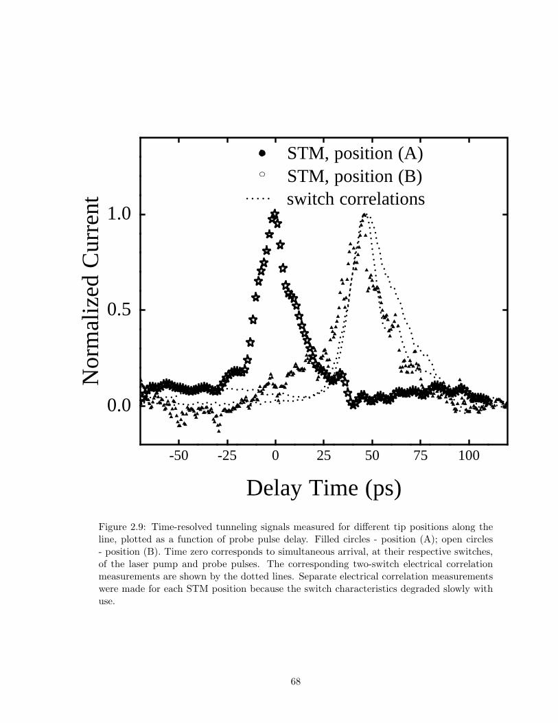
-50 -25 0 25 50 75 100
Delay Time (ps)
0.0
0.5
1.0
Nor
mal
ized
Cur
rent switch correlations
STM, position (A)STM, position (B)
Figure 2.9: Time-resolved tunneling signals measured for different tip positions along theline, plotted as a function of probe pulse delay. Filled circles - position (A); open circles- position (B). Time zero corresponds to simultaneous arrival, at their respective switches,of the laser pump and probe pulses. The corresponding two-switch electrical correlationmeasurements are shown by the dotted lines. Separate electrical correlation measurementswere made for each STM position because the switch characteristics degraded slowly withuse.
68

and improved electrical geometries.
References
[1] S. Weiss, D. F. Ogletree, D. Botkin, M. Salmeron, and D. S. Chemla. Appl.
Phys. Lett., 63:2567, 1993.
[2] R. H. M. Groeneveld, Th. Rasing, L. M. F. Kaufmann, E. Smalbrugge, J. H.
Wolter, M. R. Melloch, and H van Kempen. J. Vac. Sci. Tech. B, 14:861, 1996.
[3] M. R. Freeman and Geoff Nunes, Jr. Appl. Phys. Lett., 63:2633, 1993.
[4] Geoff Nunes, Jr. and M. R. Freeman. Science, 262:1029, 1993.
[5] David H. Auston. IEEE J. Quantum Electron., QE-19:639, 1983.
[6] A. Y. Elezzabi, J. Meyer, and M. K. Y. Hughes. Appl. Phys. Lett., 66:402, 1995.
[7] David C. Fortin. STM from planning to scanning. Technical report, University
of Alberta, 1995.
[8] C. Julian Chen. Introduction to Scanning Tunneling Microscopy. Oxford Uni-
versity Press, New York, 1993.
[9] M. B. Johnson, T. C. McGill, and N. G. Paulter. Appl. Phys. Lett., 54:2424,
1989.
[10] Rickard E. Matick. Transmission lines for digital and communication networks.
McGraw-Hill, New York, 1969.
[11] G. M. Steeves, A. Y. Elezzabi, and M. R. Freeman. Appl. Phys. Lett., 70:1909,
1997.
[12] K. Takeuchi and Y. Kasahara. Appl. Phys. Lett., 63:3548, 1993.
[13] D. Botkin, J. Glass, D.S. Chemla, D.F. Ogletree, M. Salmeron, and S. Weiss.
Appl. Phys. Lett, 69:1321, 1996.
69

[14] R.H.M. Groeneveld and H. van Kempen. Appl. Phys. Lett., 69:2294, 1996.
[15] G. Chui and J. M. Halbout. US patent, No. 5,019,707.
[16] T. Hesjedal, E. Chilla, and H.-J. Frohlich. Appl. Phys. Lett., 69:354, 1996.
[17] M. Lambsdorff, J. Kuhl, J. Rosenzweig, A. Axmann, and Jo. Schneider. Appl.
Phys. Lett., 58:1881, 1991.
[18] J. G. Simmons. J. Appl. Phys., 34:238, 1963.
[19] G. P. Kochanski. Phys. Rev. Lett., 62:2285, 1989.
[20] R. Moller, U. Albrecht, J. Bonenberg, B. Koslowski, P. Leiderer, and K. Drans-
feld. J. Vac. Sci. Technol. B, 9:506, 1991.
[21] C. Sammet, M. Volcker, W. Krieger, and H. Walther. J. Appl. Phys., 78:6477,
1995.
70

Chapter 3
Nanometer-scale imaging with anultrafast scanning tunnelingmicroscope
3.1 Context
As the “Advances in picosecond scanning tunneling microscopy via junction mix-
ing” [1] paper was being prepared for publication there were two significant devel-
opments in the field which were to stimulate the direction of subsequent experi-
ments. The first was the publication of “Advances in ultrafast scanning tunneling
microscopy” [2] by Weiss et al.. This publication reported 900 fs temporal resolu-
tion with inferred 10 nm spatial resolution using the photo-gated technique. These
results suggested that the photo-gated technique was the fastest TR-STM technique
in the world motivating us to examine the speed limitations of our junction mix-
ing technique. The second development was much more significant, the publication
by Groeneveld and van Kempen of “The capacitive origin of the picosecond electrical
transients detected by a photoconductively gated scanning tunneling microscope” [3].
In this seminal work, Groeneveldt and van Kempen developed an accurate model of
the relevant circuits involved in PG-STM. One critical feature of this model was
the incorporation of the repetitive pump/probe pulses which contribute to charg-
ing effects over time scales larger than the duty cycle of the lasers used in earlier
experiments. With this model, Groeneveldt and van Kempen concluded that the
71

photo-gated technique measured a signal which was fundamentally capacitive in o-
rigin! This reclassified PG-STM as a capacitive microscopy implying that it lacked
ultimate STM spatial resolution in the time-resolved signal.
These results stressed the need for us to improve the speed of our transmission line
structures in further time-resolved experiments, but more importantly they focused
our attention on the issue of combined temporal-spatial resolution. Many groups at-
tempting to use the PG-STM technique focused primarily on ultrafast time resolution,
assuming that STM spatial resolution would necessarily follow. The Groeneveldt, van
Kempen paper showed that in the case of PG-STM this was not so. Further efforts
to establish JM-STM should aspire to improve time resolution while demonstrating
the combined spatio-temporal resolution of the technique.
With these requirements in mind a new experiment was developed which would
test the ability of the junction mixing technique to show spatio-temporal resolution.
In past experiments the STM would tunnel into a transmission line while electrical
pump/probe pulses were launched into the tunnel junction. The spatial extent of
these electrical pulses is on the order of millimeters too large for the STM to resolve.
To achieve spatial resolution in the time-resolved signal it would be necessary to scan
the STM over a surface anomaly which would alter the time-resolved signal. If the
time-resolved signal changed over the same length scale as the size of the anomaly,
then this length scale would determine the resolution of the time-resolved signal.
With this in mind, an experiment was developed, which would pattern µm sized dots
of differing material onto the gold transmission line. By choosing the dot material
for high I/V contrast with respect to gold, the time-resolved signal mixed in the
tunnel junction between the STM tip tunneling into the gold transmission line versus
this other material would also show contrast. By scanning the STM tip between the
gold transmission line and the dot, we hoped to see a significant contrast in time-
72

Figure 3.1: Transmission line structure generated by the stmtrl.dwg mask. Note thatthere are interdigitated fingers between both vertical line segments and the main horizontaltransmission line
resolved signal, even though the DC tunneling current would remain unchanged in
the transition.
At the outset of this work, it was necessary to create two complimentary masks for
producing the transmission line substrates. One mask would be used to photolitho-
graphically define the basic transmission line structure. The first mask is a modified
version of the mask used in Ref. [1]. The basic unit in the mask is shown in Figure 3.1.
This structure is 2 cm long(along the central transmission line) and 1 cm wide.
The mask was designed using Autocad(file : stmtrl.dwg ) and produced by Adtek
Photomask. The mask was a chromium mask on a soda lime glass substrate, the
minimum feature size used in this mask was 2 µm so a quartz substrate was not
necessary. The mask was generated optically. Gaps between the vertical bias leads
and the transmission line have been replaced by interdigitated fingers as in Ref. [4]
73

Figure 3.2: The complementary mask to that shown in Figure 3.1 where the sets of trans-parent triangles are used to align the mask over the transmission line structure and theclear rectangles represent a large array of 2µm square dots separated by 3µm.
74

Figure 3.3: SEM image of the 5 µm interdigitated fingers between the 200µm main horizon-tal transmission line and the vertical line segments, referred to in the caption of Figure 3.1.
and the vertical leads were rounded to reduce electrical reflections in the structure.
An SEM image of the interdigitated fingers is shown in Figure 3.3.
The second, complimentary mask, shown in Figure 3.2. was also created using
Autocad(file : stmsq-b1.dwg 1 ) and consisted of pairs of triangular alignment marks
and over 80,000 2 µm2 squares per transmission line(40,000 dots per patch on the
transmission line). In creating our structures the first mask was used to pattern a
gold transmission line structure onto our ion implanted GaAs substrate(implant dose
was 1×10⁻¹⁵cm−2 at 200 keV) using standard photolithography. Once this was done,
photoresist was spun onto the patterned substrate and the second mask was aligned.1The autocad file contains the alignment marks for one transmission line structure and one set of four
dots, the dot pattern must be stepped and repeated to fill the space between horizontal alignment trianglesand the whole file must be stepped and repeated to create a mask paired with the one created from stmtrl.dwg
75

The mask was aligned such that the vertical bias leads of the transmission line were
positioned between the vertical pairs of triangles. This allows positioning of the
second mask in the horizontal direction. By lining the horizontal transmission line of
the patterned substrate between the horizontal pairs of triangles, vertical alignment
is achieved. The long horizontal rectangles shown in Figure 3.2 are filled with the 2
µm2 dots, so that the second mask will produce huge arrays of dots in the photoresist
on the patterned substrate. Once the photoresist is exposed and developed, there
will be an array of holes in the resist above the transmission line. By depositing
a film into the holes and over the photoresist and then removing the photoresist, a
patterned array of dots will remain. This technique is known as liftoff, and the result
of the procedure for patterning chromium dots onto a gold transmission line structure
is shown in Figure 3.4.
To provide contrast in the time-resolved signal tunneling into gold versus into a dot
it was necessary to carefully choose the material with which to fabricate the dots. We
planned on sputtering this material into the photoresist holes, so we wanted to choose
a material which was available and could easily be sputtered(note: It was subsequently
learned that evaporation is a more effective method of deposition for liftoff, as it is
more directional with poorer sidewall coverage of the holes, an asset in the subsequent
photoresist etching process). Contrast in time-resolved signal could easily be achieved
if there was contrast in the relevant domain of the I/V tunneling characteristics. I/V
characteristics had been obtained for tunneling into gold transmission lines in ambient
conditions, so we began acquiring I/V characteristics of other available metals for
comparison with gold. Experiments using titanium quickly demonstrated significant
contrast with gold. For a comparison of I/V characteristics see Figure 3.9. Because
of this striking contrast titanium dots were the first to be fabricated and tested.
Initial STM attempts to image the titanium dots were hampered by the size of
the titanium dots and their spacing(2 µm dots spaced 3 µm apart). Efforts were
76

Figure 3.4: An array of 2µm chromium dots, patterned onto a gold transmission line. Theedge of the gold transmission line, and the underlying GaAs substrate can be seen on eitherside of this SEM image.
77

made to minimize the size of the dots and using optically fabricated masks, 2 µm2
dots were at the technological limit. E-beam masks were another option, but the
write time to produce multiple arrays of hundreds of thousands of dots would make
an e-beam mask prohibitively expensive. The scan range of our STM was about 5
µm2 but any tilt of the sample would cause the microscope to move out of the range
of its feedback electronics. Because of this problem, software was developed which
would identify sample tilt in an initial small area scan, and compensate for this tilt
in subsequent larger scans. Non-linearities of piezo displacement with applied voltage
were also identified and corrected for using this software. 2 Once this software was
implemented, titanium dots could be imaged. Many images were acquired such as is
shown in Figure 3.11 (a). But through multiple scans the surface of the titanium dot
appeared to be changing. A vivid demonstration of this is shown in Figure 3.5 and
Figure 3.6.
Figure 3.5 shows a 2.76 µm STM topographic image of a titanium dot pat-
terned onto a gold transmission line (mr050922.d97). Between that figure and Fig-
ure 3.6, the STM scan range was decreased to 0.92 µm and multiple scans were
taken (mr050929.d97; mr050932.d97; mr050934.d97; mr050939.d97; mr050944.d97;
mr050947.d97). The final 2.76 µm image (mr050950.d97) was then acquired exhibit-
ing considerable changes in surface topology. All scans were done with a 35 mV bias
voltage and STM current set to 0.5 nA. From Figure 3.6 it is clear to see the affected
patch on the dot, appearing as a dip in surface topography, caused by a decrease
in conductivity in that region. Since samples with titanium dots had been fabricat-
ed it was decided to proceed with these samples even though they oxidized through
repeated scanning.
Initial time-resolved spatial images of the structures were created using the ex-
perimental setup shown in Figure 2.5 where the improved transmission line struc-2The program “STM Scan w/N-Regression v3.4” is described on page 152 in A.3 of the Appendix.
78

Figure 3.5: 2.76 µm by 2.76 µm, z range 50 nm scan of a 2µm titanium dot patterned ontoa gold substrate. Tunneling performed at 35 mV bias voltage, 0.5 nA tunneling current.
79

Figure 3.6: 2.76 µm by 2.76 µm, z range 50 nm scan of the same titanium dot shown inFigure 3.5 where a square section has been repeatedly scanned with the STM. Tunnelingperformed at 35 mV bias voltage, 0.5 nA tunneling current.
80

0
0.2
0.4
0.6
0.8
0 20 40 60 80 100Delay Time(ps)
Tim
e-R
esol
ved
Cur
rent
(pA
)Time-resolvedpoint scan
Time-resolvedimage scan times
AB
CD
E
F
G HI
Figure 3.7: Time-resolved STM current measurement. This timing trace was used to mapout the passing of pump/probe pulses past the tunnel junction of the STM. Points labelledA-I mark the times of subsequent time-resolved image scans shown in Figure 3.8.
tures described above were used. Laser pulses created pump and probe electrical
pulses which were transmitted along the central gold transmission line towards the
STM tunnel junction. Measuring the time-resolved current at a single point yielded
the time-resolved current trace shown in Figure 3.7. Times were chosen from this
trace(indicated by the diamond markers) at which to perform time-resolved image
scans. Once these delay times were selected, the optical delay line was set to the
correct offset and an image would be acquired. Images were taken as 64×64 grids
of tunneling current, feedback signal(topography), and time-resolved current(as mea-
81

sured using a lock-in amplifier). The tunneling conditions were 0.5 nA current and
-30 mV bias,3 the photoconductive switches were biased to -30 V and the lock-in time
constant was set to 100 ms. The scan program was set to wait 150 ms per point,
which is quite fast and could result in some blurring of the time-resolved signal. The
image frames for the times shown in Figure 3.7 are shown in Figure 3.8. The images
in this figure represent the first STM movie!
3.2 Publication
G. M. Steeves, A. Y. Elezzabi and M. R. Freeman, Appl. Phys. Lett. 72, 504(1998).
Ultrafast optical pump-probe techniques offer the possibility of studying many
physical phenomena on picosecond and femtosecond time scales with a temporal res-
olution limited only by the duration of the laser pulse. The shortest laser pulses are
now on atomic time scales [5], however atomic-scale spatial resolution still requires
non-optical techniques such as scanning tunneling microscopy (STM). STM applica-
tions, on the other hand, have largely been restricted to the study of static surface
properties (topography and electronic structure), revealing little information about
the dynamics underlying the phenomena under investigation. An ultrafast STM, with
temporal information added as an observable quantity, would be a valuable addition
to the arsenal of tools for studying nanometer-scale systems.
To address the need for such a device, two experimental schemes have been pro-
posed and demonstrated as possible candidates for the operation of an ultrafast STM:
photoconductively gated STM (PG-STM) [2, 6, 7] and junction mixing STM (JM-
STM) [8, 9, 10, 1]. Even though subpicosecond temporal resolution was demonstrated
with the PG-STM technique, a major concern is the demonstration of ultrafine spatial
resolution. Recently, Groeneveld et al. [3] showed that PG-STM is really a (tunneling-
stabilized) scanning capacitance microscopy, and cannot be expected to yield the fine3we found that the titanium surface would not oxidize as quickly with negative bias voltages
82
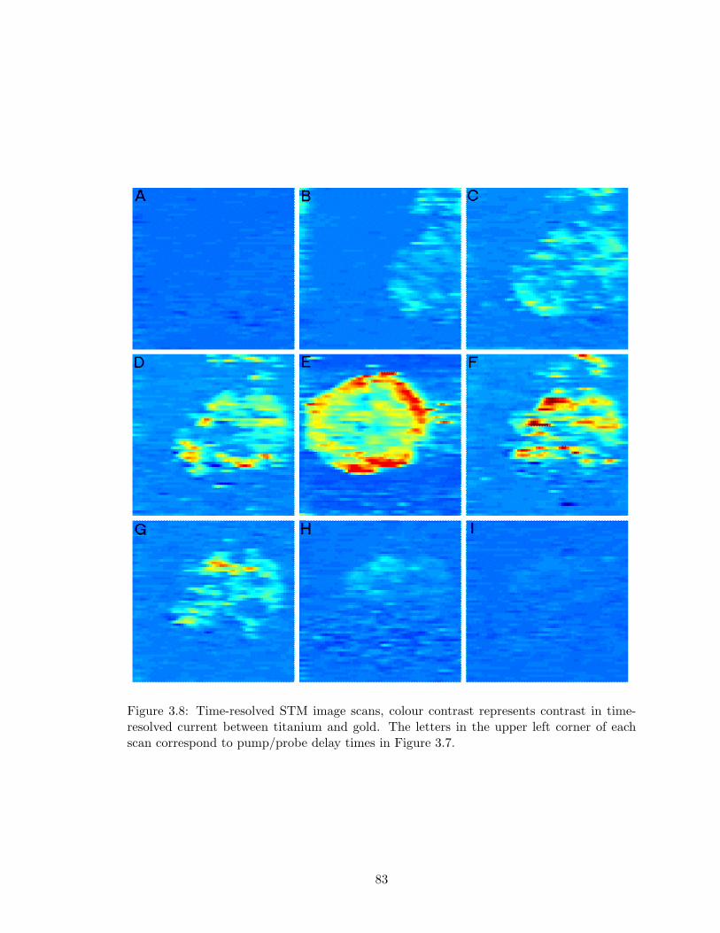
Figure 3.8: Time-resolved STM image scans, colour contrast represents contrast in time-resolved current between titanium and gold. The letters in the upper left corner of eachscan correspond to pump/probe delay times in Figure 3.7.
83

lateral resolution of STM (although it still can have useful applications [11]). In
JM-STM all the evidence points to a tunnel junction origin of the signal, but a final
and unambiguous confirmation can only be obtained through a demonstration of the
spatial resolution. This paper describes a proof of principle experiment indicating
that atomic resolution should be possible in ultrafast STM.
The STM tip-metal sample tunneling current-voltage (I−V ) characteristics are sim-
ilar enough for present purposes to those of a planar metal-insulator-metal junction.
The time-dependent STM tunnel junction current-voltage relation can be expressed
as [12],
I(t) ∝ β[V (t) + γV 3(t)] + 0[V 5(t)], (3.1)
where I(t) is the tunneling current, V (t) is the tunneling voltage, β is the linear
tunneling conductance, and γ depends on the electronic structure. Mixing of ultrafast
electrical transients is employed in order to perform measurements on picosecond time
scales. The mixing allows the measurement of ultrahigh frequencies (up to THz), far
above normal STM bandwidth. In the junction mixing STM (JM-STM) technique,
one effectively has two time-dependent biases, V1(t) and V2(t), at the tunnel junction,
where one is the signal of interest and the other an electrical ”probe pulse”. Due
to the non-linear term in equation 3.1, the resultant tunneling current amplitude
I(V1(t) + V2(t)) is greater than the sum of tunneling currents of the two individual
voltage pulse amplitudes, I(V1(t)) + I(V2(t)). The time-integrated STM tunneling
current depends on the degree of the temporal overlap of V1(t) and V2(t). When the
two pulses arrive simultaneously at the tunnel junction, the detected signal is larger
than if they arrive at different times. By varying the delay between the pump and
probe pulse and recording the time-integrated current from the STM, we obtain a
correlated signal which can be deconvolved with the electrical pulses to obtain the
temporal response of the system [8, 9, 10, 1].
84

From Eq. 3.1 it can be seen that the excess current amplitude is proportional to γ.
A direct test of spatial resolution in the method can thus be performed by preparing a
test surface having electronic structure contrast, created by patterning metal surfaces
with distinct I − V non-linearities. By measuring the time-resolved signal across an
edge between the two distinct surfaces, we can estimate the spatial resolution of the
time-resolved measurements. The observed signal step will represent an upper bound
on the ultimate resolution of the technique, as it may also be limited by the edge
definition of the sample itself.
For the present tests, we developed a structure consisting of titanium dots on a
gold surface. Figure 3.9 illustrates the I − V curves for both gold and titanium films
measured at a fixed linear tunneling conductance β = 23 nS. The measurements are
carried out with the STM operating under ambient conditions. The values of γ can
be determined by fitting the experimental data to equation 3.1, yielding γ = 1.3V −2
and 44V −2 for the Au and Ti surfaces, respectively. The ratio of the γ’s is large,
making the two surfaces an attractive choice because good contrast is expected in the
time-resolved signal.
The details of experimental setup are described in Ref. [1]. The primary compo-
nent is a high-speed transmission line, which is shown schematically in Figure 3.10.
The structure is designed to reduce the dispersion of the picosecond pulses and to
enhance the amount of the photogenerated current. The structure consists of three
100 nm thick, 200 µm wide Au lines spaced 5 mm apart on a semiconductor substrate.
These lines are fabricated photolithographically on an H+ ion-implanted GaAs semi-
insulating substrate (dosage of 1× 10⁻¹⁵cm−2 at 200 keV). A pair of 2 µm gap inter-
digitated GaAs photoconductive switches are fabricated on each side of the central
Au transmission line. Using the ion dosage of 1 × 10⁻¹⁵cm−2, the expected carrier
lifetime of the photoconductive switches is of order 1 ps. However, the switches seem
85
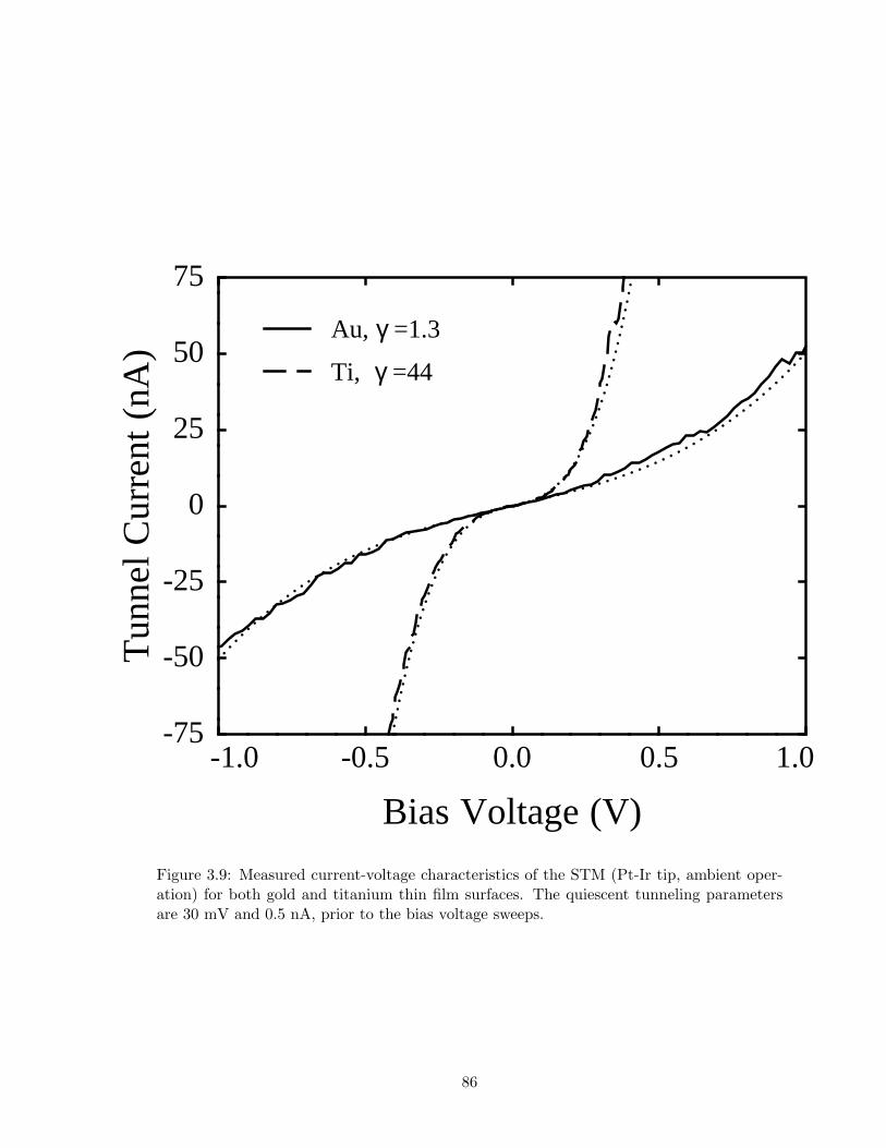
-1.0 -0.5 0.0 0.5 1.0
Bias Voltage (V)
-75
-50
-25
0
25
50
75
Tun
nel
Cur
rent
(nA
)
Au, γ =1.3
Ti, γ =44
Figure 3.9: Measured current-voltage characteristics of the STM (Pt-Ir tip, ambient oper-ation) for both gold and titanium thin film surfaces. The quiescent tunneling parametersare 30 mV and 0.5 nA, prior to the bias voltage sweeps.
86

Figure 3.10: Schematic illustration of the high-speed Au transmission line and the interdig-itated photoconductive switches. A scanning electron micrograph shows the Ti dot patternatop the transmission line on an expanded scale.
87

Figure 3.11: (a) A topographic STM image of a typical 3 µm × 3µm Ti dot used in themeasurements. (b) A time-resolved STM image of another Ti dot taken at 0 ps.
to age quite rapidly and during the measurements reported here the electrical pulse
width was approximately 20 ps. In order to test the spatial resolution of the STM,
any array of 20 nm thick Ti micro-dots (nominally 3 µm squares) are patterned by
photolithography and lift-off along the central Au transmission line.
Figure 3.11(a) shows a topographic STM image of a Ti dot, acquired at a constant
tunneling current of 0.5 nA. After locating a dot through normal scanning, the STM
is switched to time-resolved mode through pulsed illumination of the photoconductive
switches. The optical delay line is scanned to determine the exact probe-pulse time
delay position for maximal electrical pulse overlap at the tunnel junction for this tip
location along the transmission line. This delay line position is labeled as time ’0
ps’ and is used as a time-reference point throughout the experiment. Figure 3.11(b)
shows a coarse spatial scan of the time-resolved signal in the vicinity of a Ti dot
at 0 ps. The Ti dot structure is observed with good contrast, as anticipated. The
lock-in time constant was 300 ms for this 64×64 pixel image, which took 25 minutes
to acquire.
88

Figure 3.12: Higher resolution views of a Au/Ti edge. (a) topographic (b) time-resolved atprobe delays of 10, 20, and 25 ps.
Higher resolution scans of the step edge are shown in Figure 3.12. Another to-
pographic scan is shown in panel (a), accompanied in panel (b) by line-scans of the
time-resolved signal taken across the central part of the topographic image. A series
of spatial scan traces are shown at delay times of 10, 20, and 25 ps. As the probe
electrical pulse is delayed relative to the pump, the measured signal amplitude or im-
age strength decreases until the signal disappears when there is no longer significant
pulse overlap at the tunnel junction.
Finally, by focusing the microscope on the step edge at t = 0 as shown in Fig-
ure 3.13, we can obtain a bound on the spatial resolution in time-resolved mode of 10
nm. We do not expect with such a structure to be able to place a limit on resolution
89

Figure 3.13: Zoom-in on the time-resolved signal at the step-edge at t = 0 ps.
90

much better than the 20 nm thickness of the Ti dot, owing to the lithographic defi-
nition of the edge. This observation of the edge boundary of the Ti structure at our
expected limit of resolution reinforces the conclusion that the tunneling signal alone
is time-resolved in these experiments. The geometrical capacitance between the STM
tip and the sample does not play a role in limiting or degrading the spatial resolution
in the operation of a JM-STM [8, 9, 10, 1].
In summary, we have presented experimental results that demonstrate the spatio-
temporal operation of a JM-STM. In particular, picosecond time-domain measure-
ments of electronic structure have been obtained with a fine spatial resolution of
10 nm. This demonstration of nanometer-scale imaging in ultrafast STM is another
significant step towards the ultimate goal of atomic resolution on ultrafast time scales
References
[1] G. M. Steeves, A. Y. Elezzabi, and M. R. Freeman. Appl. Phys. Lett., 70:1909,
1997.
[2] D. Botkin, J. Glass, D.S. Chemla, D.F. Ogletree, M. Salmeron, and S. Weiss.
Appl. Phys. Lett, 69:1321, 1996.
[3] R.H.M. Groeneveld and H. van Kempen. Appl. Phys. Lett., 69:2294, 1996.
[4] A. G. Foyt, F. J. Leonberger, and R. C. Williamson. Appl. Phys. Lett., 40:447,
1982.
[5] A. Baltuska, Z. Wei, M. S. Pshenichnikov, and D. Wiersma. Opt. Lett., 22:102,
1997.
[6] R. H. M. Groeneveld, Th. Rasing, L. M. F. Kaufmann, E. Smalbrugge, J. H.
Wolter, M. R. Melloch, and H van Kempen. J. Vac. Sci. Tech. B, 14:861, 1996.
[7] U. D. Keil, J. R. Jensen, and J. M. Hvam. Appl. Phys. Lett., 70:2625, 1997.
91

[8] Geoff Nunes, Jr. and M. R. Freeman. Science, 262:1029, 1993.
[9] M. R. Freeman and Geoff Nunes, Jr. Appl. Phys. Lett., 63:2633, 1993.
[10] M. R. Freeman and Nunes G., Jr. Appl. Surf. Sci., 107:238, 1996.
[11] J. R. Jensen, U. D. Keil, and J. M. Hvam. Appl. Phys. Lett., 70:2762, 1997.
[12] J. G. Simmons. J. Appl. Phys., 34:238, 1963.
92

Chapter 4
Circuit Analysis of an UltrafastJunction Mixing ScanningTunneling Microscope
4.1 Context
The “Nanometer-scale imaging with an ultrafast scanning tunneling microscope” [1]
was well received. Attention was drawn to this work through an article in Physics
World [2]. Many groups continued to use the Photo-gated technique as it had gar-
nered some inertia, regardless of its inferior spatial resolution. In order to further
understand the limitations on the junction mixing technique we endeavored to build
a simple circuit element model of the STM tunnel junction. This model was based
on the circuit illustrated in Figure 4.2. Details of this model and current calculations
from it will now be given.
The basic equation of interest solves the tunneling current equation for detected
current through the tunnel junction of the STM. Initially we introduce a time-varying
voltage on the transmission line V (t) and the current I(t) measured at the output of
the microscope. The current component passing through the capacitor is Ic(t) and
through the nonlinear tunnel resistance Rt(V )(see equation 1.27) is Ir(t). Referring
to Figure 4.2 we see that charge on the transmission line can dissipate by flowing
through the effective resistance of the tunnel junction, charge can also store in the
93
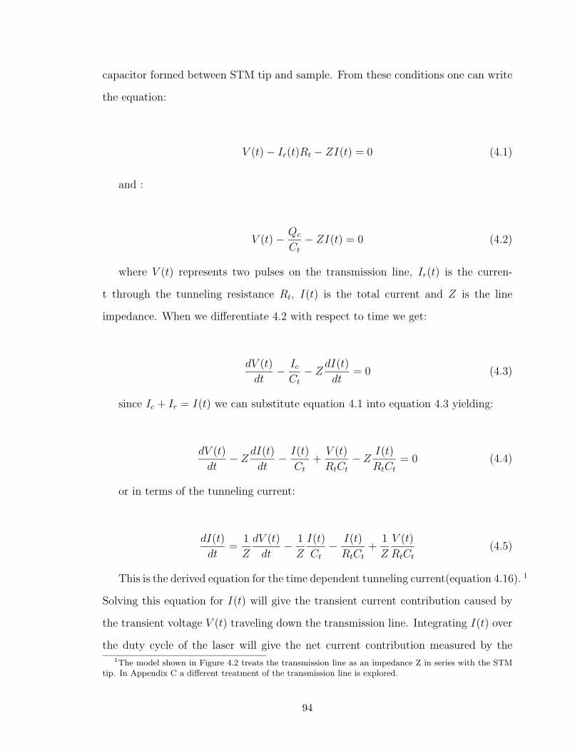
capacitor formed between STM tip and sample. From these conditions one can write
the equation:
V (t)− Ir(t)Rt − ZI(t) = 0 (4.1)
and :
V (t)− Qc
Ct− ZI(t) = 0 (4.2)
where V (t) represents two pulses on the transmission line, Ir(t) is the curren-
t through the tunneling resistance Rt, I(t) is the total current and Z is the line
impedance. When we differentiate 4.2 with respect to time we get:
dV (t)
dt− IcCt− ZdI(t)
dt= 0 (4.3)
since Ic + Ir = I(t) we can substitute equation 4.1 into equation 4.3 yielding:
dV (t)
dt− ZdI(t)
dt− I(t)
Ct+V (t)
RtCt− Z I(t)
RtCt= 0 (4.4)
or in terms of the tunneling current:
dI(t)
dt=
1
Z
dV (t)
dt− 1
Z
I(t)
Ct− I(t)
RtCt+
1
Z
V (t)
RtCt(4.5)
This is the derived equation for the time dependent tunneling current(equation 4.16). 1
Solving this equation for I(t) will give the transient current contribution caused by
the transient voltage V (t) traveling down the transmission line. Integrating I(t) over
the duty cycle of the laser will give the net current contribution measured by the1The model shown in Figure 4.2 treats the transmission line as an impedance Z in series with the STM
tip. In Appendix C a different treatment of the transmission line is explored.
94

lock-in amplifier. V (t) is given by adding two voltage pulses together where the time
separation between each voltage pulse is t0. The form of one of the voltage pulses is
given by equation 4.17:
V1(t) = V0
∫ t
−∞sech2
(τ
tp
)exp
(τ − ttc
)dτ (4.6)
where V0 is the amplitude of the voltage pulse and t0 = 0. This equation can be
solved analytically with a solution in terms of hypergeometric functions2:
2F1
1, 2; 2 +
1
tp;
1
e−t + 1
×
sech2 t2
1 + 1tp
(4.7)
A series of electrical pulses for different pulse-widths can been seen in Figure 4.1.
Summing two such pulses with different relative arrival times at the tunnel junction
gives us our function V (t). In order to evaluate I(t) we still need to calculate the
geometrical tip/sample capacitance C. Using a finite element model based on the
method of images, Dr. R. A. Said was able to calculate the tip sample capacitance
for a model STM tip at tip/sample separations from 21 → 2 nm. Details of this
calculation can be found in Dr. Said’s thesis [3]. Extension of this calculation down
to A length scales was not possible as the element size used in the calculation was 2
nm. In order to calculate the capacitance at A separations the Said model was fit with
a 2 capacitor system where the bulk of the STM tip was treated as a single parallel
plate capacitor, and the apex of the tip as another parallel plate capacitor. This
model was fit to the Said data and then extended down to 2 A tip/sample separation
as shown in Figure 4.3. From the fit it was clear that a value of 33 fF would suffice to
capture the geometrical capacitance of the tip/sample system. The effect of varying
this capacitance by small fractions is negligible and the effect of large variations in
capacitance is shown in Figure 4.5.
Once the capacitance and the voltage pulse V (t) are known we can calculate the
current pulse I(t). The current pulse was calculated by Bob Teshima using the2In mathematica this is expressed as: Hypergeometric2F1[1,2,2+1/pulsewidth,1/(Exp[-
t]+1)]*(Sech[t/2]*Sech[t/2])/(1+1/pulsewidth)
95

-20 -10 10 20 30
0.5
1
1.5
2
2.5
3C
-20 -10 10 20 30
0.5
1
1.5
2
2.5
3D
-20 -10 10 20 30
0.5
1
1.5
2
2.5
3A
-20 -10 10 20 30
0.5
1
1.5
2
2.5
3B
travelling_pulse.nb 1
Figure 4.1: Electrical pulses with pulse widths(due to carrier recombination) a) 3 ps; b) 6ps; c) 9 ps; d) 12 ps.
96

following approach. First it was rewritten in the form:
dI(t)
dt=
1
Z
dV (t)
dt− I(t)
ZCt+V (t)− I(t)Z
RtZCt(4.8)
=1
Z
dV (t)
dt− I(t)
ZCt+ β
((V (t)− I(t)Z) + γ(V (t)− I(t)Z)3
ZCt
)(4.9)
= y0(t) + βy1(t) (4.10)
where y0(t) and y1(t) represent two components of the tunneling current. The AC
component of the current is y0(t) and integrates to zero as no DC current can flow
through a capacitor. The integral of the second component y1(t) is what we will
concern ourself with. The factor β was removed from y1(t) so that it will be more
comparable to y0(t) in magnitude and any comparative computations between the
two will be less susceptible to errors. The differential equation for y1(t) is:
dy1
dt=
1
Z
dV (t)
dt− y1
ZCt(4.11)
Substituting f0 = V (t)− y1Z we get:
df0
dt=V (t)− f0
ZCt(4.12)
which can be solved in terms of hypergeometric functions. The equation for the
integrated current which we are interested in can be expressed in terms of V (t) and
f0 as:
∫ ∞−∞
y1(t) =
∫ ∞−∞
V (t)dt+ γ
∫ ∞−∞
f 20 (t)V (t)dt (4.13)
This equation was solved by substituting the hypergeometric function solutions for
V (t) and then numerically integrating the right hand side of equation 4.13, using a
4th order Runge-Kutta solver. The limits of integration in equation 4.13 were chosen
97

far enough from the current pulse that its amplitude was negligible. By multiplying
the integral by β we can recover the total charge transferred to the STM tip. This
charge is acquired over the duty cycle of the laser, giving us a net contribution to the
tunneling current. A Fortran program was written by Bob Teshima to evaluate the
integrated current for different input parameters.
4.2 Publication
G. M. Steeves, A. Y. Elezzabi, R. Teshima, R. A. Said, and M. R. Freeman, IEEE J.
Quantum Electron. 34, 1415(1998).
Time-resolved scanning tunneling microscopy (TR-STM) will enable the study of
dynamics in nanostructures on picosecond to femtosecond time scales. Scanning tun-
neling microscopes are used in atomic resolution studies of surface and electronic
structure. These studies are often performed on materials found in semiconductor
devices. With TR-STM, the ultrafast electrical dynamics of surfaces and devices can
also be examined in a non-invasive fashion. For example, electron transport might
be studied directly in single electron transistors or across a Coulomb blockade struc-
ture. Many techniques to add ultrafast time resolution to an STM have been pro-
posed [4, 5, 6, 7, 8, 9, 10, 11]. Previous work has indicated that direct modulation of
the STM tunnel junction may be the only way to maintain excellent spatial resolution
in a time-resolved experiment. Two methods to directly modulate the junction have
been proposed; varying the tip sample separation [5, 9] and electrically modulating the
junction [4, 12, 13]. Of these techniques, electrical modulation is the only one, having
the necessary speed for sub-picosecond time resolution. The electrical modulation of
the STM tunnel junction for TR-STM is known as junction mixing scanning tunnel-
ing microscopy(JM-STM). Currently, JM-STM is the only time-resolved technique
with demonstrated nanometer spatial resolution combined with picosecond temporal
resolution [13].
98

Figure 4.2: Equivalent JM-STM lumped RC circuit.
In an effort to further characterize the ultrafast operation of the JM-STM, a circuit
model has been developed. Following the analysis of Groeneveld and van Kempen for
another implementation of ultrafast STM [2], the JM-STM experiment is modeled as
a lumped element RC circuit excited with ultrafast transient electrical pulses. With
this circuit model we attempt to predict the ultrafast operation of the JM-STM, and
support our predictions with previous experimental results.
The basic circuit is illustrated in Figure 4.2 3; it consists of two ultrafast photocon-
ductive switches connected in parallel to each other and in series with a high-speed
transmission line which has an impedance, Z. The switches are biased to a voltage
V0 and are triggered by laser pulses to launch the time-dependent electrical pulses
V1(t) and V2(t − t0). Coupled to the transmission line is the RC part of the circuit
that describes the STM tunnel junction. The tunnel junction impedance is modeled
as a non-linear resistance, Rt(V ). A vital parameter to the model calculation is the
magnitude of the geometrical capacitance between the tip and the microstrip line.3The published work presented here, originally included a different version of this figure. In the publica-
tion, an additional impedance Z, passing current to ground, was included on the transmission line after theSTM tip. The calculations presented in this chapter and in the publication did not include this additionalimpedance. The affect of this impedance has been explored in Appendix C.
99

The magnitude of this capacitance is difficult to measure directly since it is typically
in the fF range [2]. Most calculated values of the capacitance break down in the
tunneling region where they diverge for small tip/sample separation. It is not clear
exactly how capacitance will scale as the tip/sample separation approaches zero in a
normal tunneling experiment (S. Kurokawa and A. Sakai have examined this problem
in great detail [14, 15]). To approach this problem, the method of images was used to
calculate the capacitance for a range of tip/sample separations down to 2 nm. These
results were fit and then extrapolated into the tunneling regime by approximating the
tip as 2 parallel plate capacitors with different separations and effective areas. The
STM tip geometry used in the initial image calculation resembles the experimental
STM tip geometry and is shown in the inset of Figure 4.3. The capacitance Ct is
evaluated by calculating the induced surface charge distribution due to the applied
electric potential.
The electrostatic potential for a surface charge of density σ(~r0) over a ground plane
can be expressed in terms of the static integral equation
φ(~r) =
(1
4πε0
)∫ ∫S
σ(~r0)
[1
|~r − ~r0|− 1
|~r − ~r0′|
]dS (4.14)
where φ(~r) is the potential at distance ~r from the origin, ~r0 is a point on the conducting
surface, ε0 is the permittivity of free space and dS is the surface element. The ground
plane is replaced by an image of the real charge distribution located at ~r0′ and
the moment method [16] is used to solve the integral equation. Once the surface
charge distribution is calculated, the capacitance is evaluated as the ratio between
the induced charge on one of the two surfaces and their potential difference.
The solid points in Figure 4.3 show the results of these capacitance calculations
evaluated at a variable tip height range between 2 - 21 nm where the minimum
separation is limited by the element size used in the calculation. To extend this down
100

Figure 4.3: Calculated tip-transmission line capacitance as a function of STM tip heightabove the transmission line. Inset schematically shows the tip geometry used in the calcu-lations.
101

to separations of fractions of a nanometer, used in tunneling, the calculated points
are fit to the expansion:
C =ε0A1
D
(1− ∆D
D+ · · ·
)+ε0A2
∆D(4.15)
The shank and taper of the probe behave as a parallel plate of effective area A1 at
a distance D to the sample. The probe tip has an effective area A2 and ∆D( D) is
the tip sample separation. The fit shown by the solid line in Figure 4.3 corresponds
to parameters A1 = (776.271µm)2, A2 = (13.8874nm)2 and D = 161.281µm. Over
a height range from 0.2 to 20 nm the capacitance only changes by one part in 103,
so we treat it as a constant with value 33 fF. This result also shows that changes
in capacitance as the tip scans over the surface will have negligible influence on the
time-resolved signal from topographic variations.
The pulse induced tunneling current I(t), developed on the STM tip, is calculated
by integrating the following differential equation:
dI(t)
dt=
1
Z
dV (t)
dt− I(t)
(1
ZCt+
1
RtCt
)+
V (t)
RtZCt(4.16)
where V (t) = V1(t) + V2(t− t0) is the sum of the voltage pulses delivered by the two
ultrafast photoconductive switches and t0 is the delay time. The time dependence of
each voltage pulse can be evaluated from a convolution between the excitation laser
pulse temporal shape and the temporal response of the photoconductive switch:
V1(t) = V0
∫ t
−∞sech2
(τ
tp
)exp
(τ − ttc
)dτ (4.17)
and
V2(t− t0) = V0
∫ t−t0
−∞sech2
(τ
tp
)exp
(τ − (t− t0)
tc
)dτ (4.18)
102

where tc is the electro-optic switch carrier recombination time, tp is the laser excitation
pulse width. The tunnel junction non-linear resistance is given by:
Rt(V ) =1
β(1 + γ(V (t)− I(t)Z)2)(4.19)
where, β and γ are the linear and non-linear tunneling conductances of the tun-
nel junction, respectively and Z is the line impedance. The excitation laser pulses
illuminate the photoconductive switch gaps at times t = 0, and t = t0.
Comparisons of the circuit model with experimental results are shown in Figure 4.4.
For the left panel, calculations are performed using a V0 = 0.49V voltage pulse and
the 10 ps JM-STM experimental conditions presented in reference [12] (β = 5.1 nS,
γ = 0.75V −2 for the Au surface, Z = 68Ω, Ct = 33 fF, tc = 10 ps , and tp = 2.8 ps).
We have numerically integrated equation 4.16 over the time interval -100 ps < t < 100
ps to calculate the pulse induced current. Since our experimental apparatus measures
a time- resolved signal which is averaged over the duty cycle of the laser, it is necessary
to scale the pulse induced current in a comparable manner. The model calculation and
the experimental result are in excellent agreement. To further test the model, we have
used new samples with faster photoconductive switches to push the temporal response
of the STM to the limit of our laser pulse width (2.8 ps). By using the measured
values of β = 23 nS, γ = 1.3V −2, tc = 4.5 ps , and tp = 2.8 ps, and a capacitance
Ct = 33 fF, we repeated the calculation for a V0 = 0.561 V voltage pulse along a
transmission line with impedance Z = 68Ω. Again, the calculated and measured 4.5
ps JM-STM response (9-ps correlation width) are in good agreement(right panel).
The difference in amplitudes between the right and left panels is due to the different
Au surface conditions used in experiments (an unfortunate consequence of ambient
tunneling) and the different pump/probe pulse widths. The discrepancy in the curve
tail between the model and the experiment is attributed to the non-ideal electrical
pulse shape in the measurements from reflections and dispersion.
103

-30 0 30Delay Time (ps)
0
1
2
3
Tim
e-R
esol
ved
Cur
rent
(pA
)
-30 0 30Delay Time (ps)
0
5
10
15
20
25 Tim
e-Resolved C
urrent (pA)
Figure 4.4: Time-resolved tunneling currents. Experimental data is indicated by dashedlines, model calculations are represented by solid lines. Left panel shows data for a 10 psvoltage pulse, right panel shows data from a faster 4ps pulse.
104
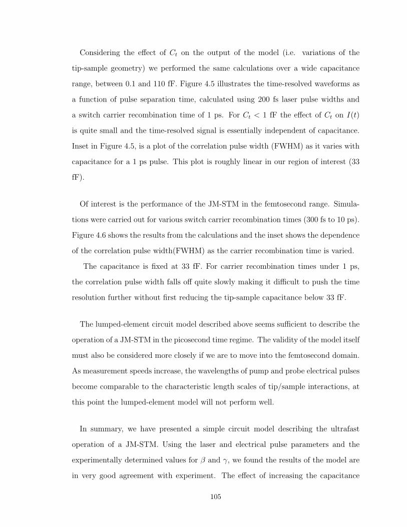
Considering the effect of Ct on the output of the model (i.e. variations of the
tip-sample geometry) we performed the same calculations over a wide capacitance
range, between 0.1 and 110 fF. Figure 4.5 illustrates the time-resolved waveforms as
a function of pulse separation time, calculated using 200 fs laser pulse widths and
a switch carrier recombination time of 1 ps. For Ct < 1 fF the effect of Ct on I(t)
is quite small and the time-resolved signal is essentially independent of capacitance.
Inset in Figure 4.5, is a plot of the correlation pulse width (FWHM) as it varies with
capacitance for a 1 ps pulse. This plot is roughly linear in our region of interest (33
fF).
Of interest is the performance of the JM-STM in the femtosecond range. Simula-
tions were carried out for various switch carrier recombination times (300 fs to 10 ps).
Figure 4.6 shows the results from the calculations and the inset shows the dependence
of the correlation pulse width(FWHM) as the carrier recombination time is varied.
The capacitance is fixed at 33 fF. For carrier recombination times under 1 ps,
the correlation pulse width falls off quite slowly making it difficult to push the time
resolution further without first reducing the tip-sample capacitance below 33 fF.
The lumped-element circuit model described above seems sufficient to describe the
operation of a JM-STM in the picosecond time regime. The validity of the model itself
must also be considered more closely if we are to move into the femtosecond domain.
As measurement speeds increase, the wavelengths of pump and probe electrical pulses
become comparable to the characteristic length scales of tip/sample interactions, at
this point the lumped-element model will not perform well.
In summary, we have presented a simple circuit model describing the ultrafast
operation of a JM-STM. Using the laser and electrical pulse parameters and the
experimentally determined values for β and γ, we found the results of the model are
in very good agreement with experiment. The effect of increasing the capacitance
105

-4 -2 0 2 4Pulse Separation Time (ps)
0
20
40
60
80
100
Pul
se In
duce
d C
urre
nt (
nA)
1 fF
2 fF
10 fF
20 fF
30 fF
40 fF
50 fF
70 fF
0 30 60 90Capacitance (fF)
0
5
10
Cor
rela
tion
Pul
se W
idth
(ps
)
Figure 4.5: Tunneling junction current time-resolved signals for different tip-transmissionline capacitance. Inset shows the width of the correlation pulses as the capacitance is varied.Model parameters are: β = 23 nS, γ = 1.3V −2, V0 = 1 V, tc = 1 ps, and tp = 200 fs.
106

-10 -8 -6 -4 -2 0 2 4 6 8 10Pulse Separation Time (ps)
0
5
10
15
Pul
se In
duce
d C
urre
nt (
nA)
1 ps
700 fs
500 fs
300 fs
0 5 10Carrier lifetime (ps)
0
5
10
15
Cor
rela
tion
Pul
se W
idth
(ps
)
Figure 4.6: Calculated time-resolved tunneling current for various electrical excitation puls-es. Inset shows the width of the correlation pulses as the width of the voltage pulse alongthe transmission line is varied. Model parameters are: β = 23 nS, γ = 1.3V −2, V0 = 1 V,Ct = 33 fF, and tp = 200 fs.
107

between tip and sample was to reduce the magnitude of the pulse induced current
while increasing the width of the time-resolved pulse. By investigating the effect of
shorter voltage pulses we see that JM-STM, at pulse widths less than 1 ps, can be
achieved only when the capacitance between tip and sample is reduced below 33 fF.
The limitations in response time of the JM-STM are caused by the capacitive loading
of the tip which reduces the effective voltage across the tunnel junction resistor Rt(V ).
To better understand the operation of a JM-STM in the femtosecond regime a more
complete electromagnetic model should be developed.
References
[1] G. M. Steeves, A. Y. Elezzabi, R. Teshima, R. A. Said, and M. R. Freeman.
IEEE J. Quantum Electron., 34:1415, 1998.
[2] R.H.M. Groeneveld and H. van Kempen. Appl. Phys. Lett., 69:2294, 1996.
[3] Ra’a A. Said. Scanning Force Potentiometry Techniques for Semiconductor Cir-
cuit Characterization. PhD thesis, University of Manitoba, 1995.
[4] Geoff Nunes, Jr. and M. R. Freeman. Science, 262:1029, 1993.
[5] M. R. Freeman and Geoff Nunes, Jr. Appl. Phys. Lett., 63:2633, 1993.
[6] S. Weiss, D. F. Ogletree, D. Botkin, M. Salmeron, and D. S. Chemla. Appl.
Phys. Lett., 63:2567, 1993.
[7] S. Weiss, D. Botkin, D. F. Ogletree, M. Salmeron, and D. S. Chemla. Phys.
Status Solidi B, 188:343, 1995.
[8] R. H. M. Groeneveld, Th. Rasing, L. M. F. Kaufmann, E. Smalbrugge, J. H.
Wolter, M. R. Melloch, and H van Kempen. J. Vac. Sci. Tech. B, 14:861, 1996.
[9] T. Hesjedal, E. Chilla, and H.-J. Frohlich. Appl. Phys. Lett., 69:354, 1996.
108

[10] W. Pfeiffer, F. Sattler, S. Vogler, G. Gerber, J. Y. Grand, and R. Moller. Appl.
Phys. B, 64:265, 1997.
[11] G. Chui and J. M. Halbout. US patent, No. 5,019,707.
[12] G. M. Steeves, A. Y. Elezzabi, and M. R. Freeman. Appl. Phys. Lett., 70:1909,
1997.
[13] G. M. Steeves, A. Y. Elezzabi, and M. R. Freeman. Appl. Phys. Lett., 72:504,
1998.
[14] S. Kurokawa and A. Sakai. Sci. Rep. RITU, 44:173, 1997.
[15] S. Kurokawa and A. Sakai. accepted for publication in J. Appl. Phys., 83, 1998.
[16] R. F. Harrington. Field Computation by Moment Method. Macmillan, New York,
1968.
109

Chapter 5
Design and Development of a LowTemperature High Vacuum STMwith Optical Access
5.1 Introduction
Following the development of the junction mixing time-resolved STM technique, ef-
forts began to demonstrate this technique on one of the real world problems that
triggered interest in the method, nonequilibrium superconductivity. The proposed
system of study was the superconducting vortex state in NbSe2. Imaging of the vor-
tex state using an STM was first accomplished by Hess et al. [1] as shown in Figure 1.4.
The goal here is to image vortex state dynamics using JM-STM, by transiently sup-
pressing superconductivity using ultra-fast optical pulses. This goal has not yet been
met. In order to image the vortex state, it was necessary to develop a new ultra-
fast, low temperature, high vacuum STM system. The design, development, and
implementation of this system will now be discussed.
The initial microscope design was based on a microscope constructed by Dhirani,
Fisher and Guyot-Sionnest [2]. The design and development process has been ongoing.
All elements incorporated into what is currently the “final” design have been modified
and refined on a continuing basis as required. For this discussion we will focus on 3 key
factors in microscope design; the mechanical and electrical designs of the microscope,
110

including the vibration isolation system and the entire electrical system down to
the power supplies for all necessary STM electronics; and the environment of the
tunneling head-shell of the microscope, specifically the vacuum system developed to
allow the microscope to function at cryogenic temperatures and with optical access for
pump/probe or laser ablation experiments. For each of these topics, the operational
requirements will be outlined as they were predicted and discovered experimentally.
5.2 Mechanical Design
The mechanical design of the STM was driven by the need to eliminate vibrational
coupling to the tunnel junction of the microscope. This consideration led us to choose
very specific materials for the construction of the microscope, along with an elaborate
vibration isolation system. The overall vibration isolation objective is to decouple the
head shell from all environmental vibrations. Since this objective cannot be met in a
terrestrial environment we attempt to isolate the head shell from all vibrations greater
than 1 Hz. If this can be done, the next requirement is to design the STM head shell
to be very rigid, such that oscillations below 1 Hz will move the entire head shell in
unison, allowing no relative motion between STM tip and sample. In this way we can
achieve the stability necessary for atomic resolution.
Figure 5.1 illustrates the main features of the present vibration isolation system.
Resting on the floor of a basement laboratory are cylindrical steel legs filled with
100 lbs of sand each. Resting on top of the sand in each leg is a top plate. These
plates support a pneumatic table. The pneumatic table supports a series of 4, 200
lb steel plates and each plate is separated by pads of ISODAMP C-1002 blue vinyl
damping material 1. The center of each plate has been cut out to allow the STM
to be lowered through the plates until the top of the microscope rests on the top of
the uppermost plate. The microscope hangs from the top of the plates into a liquid1EAR Specialty Composites (877)327-4332
111

PneumaticLegs
STM Vacuum Chamber
STM Head Shell
Stainless SteelSprings
Eddy CurrentDamping
Sand Filled Legs
Steel Plates Damping Material
Figure 5.1: STM vibration isolation system.
112
helium dewar. Vibrations in the helium dewar are decoupled from the microscope
and plates, through a flexible 60 section edge welded bellows. The head shell of the
microscope hangs from the body of the microscope from three pretensioned stainless
steel springs, and eddy current damping is used between the hanging head shell and
the vacuum can (surrounding the head shell) to dissipate head shell motion. From
the calculations of Nagaya [3] the damping force between a copper block of thickness
t and area b× d next to a cylindrical magnet with field B and area πa2 is:
Fx = −C0
(B2πa2t
ρ
)vx, (5.1)
where vx is the relative velocity between the copper block and the magnet, and ρ
is the resistivity of the copper. C0 is a dimensionless geometrical constant which is
given in [3] for various ratios of a, b and d. In the case where b, d a the constant
becomes C0 = 0.5. Stainless steel springs were chosen as they are non-magnetic and
could be pretensioned more than beryllium copper springs(a more common spring
material for non-magnetic applications).
This vibration isolation system developed through a number of iterations with
support from references such as Chen’s textbook [4]. Initial low temperature STM
designs consisted of the microscope head shell hanging on beryllium copper springs
from a short 10” platform which rested on the bottom of the cryostat. Trials with
this configuration were unsuccessful as the boiling of liquid nitrogen in the cryostat
caused sufficient vibrations to disrupt STM measurement. In order to achieve better
decoupling from these vibrations, the 1 stage decoupling system was replaced with
a 2 stage system which was suspended from the top of the cryostat. This system
had a set of springs suspending a copper weight from which 3 more springs hung to
support the STM head shell. The intermediate copper weight sported 3 permanent
magnets around its exterior. A copper ring, friction mounted within the column
of the cryostat damped the motion of the copper weight through the eddy current
damping mechanism. This isolation system was much better than its predecessor
113

but still insufficient for stable tunneling. The problem was that the microscope was
still directly coupled to the cryostat as it was hanging from the top of the cryostat.
These factors forced us to consider an isolation system in which the microscope was
decoupled from both mechanical resonances in the building and from boiling induced
oscillations in the cryostat. Hence we settled on the current scheme of hanging the
microscope from a vibration isolation table, into the cryostat.
The rigid STM head shell was constructed using a heavy (≈ 700 grams) oxygen
free high conductivity(OFHC) copper puck. Copper was used due to its density,
electrical and thermal conductivity and compatibility with high vacuum applications.
An L-shaped bracket is screwed onto the top of the puck to support the STM tip
assembly and a circular cut out on the top of the puck accommodates the STM
approach assembly. This modular design allows us to easily replace or modify the
approach and scanning assemblies without re-machining the head-shell. The tip and
approach assembly are fixed to the head shell using set screws, machined along one
edge to eliminate trapped air pockets. An array of tapped holes was machined into the
copper puck to allow wiring and other devices such as a low temperature thermometer
to be fastened down to the head-shell. The copper puck, tip assembly and approach
assembly are shown in Figure 5.2.
The approach assembly can be seen in the left view of Figure 5.2. This assembly
consists of a white macor disc with 3 short piezo tubes(18” OD) glued into the disc.
Macor is a machinable ceramic material produced by Dow Corning, which is very
rigid and an excellent electrical insulator. The tops of the piezo tubes are capped
with ruby balls, to provide a hard smooth surface for the sample sled to rest on. The
whole assembly is fixed into the copper puck by means of 2 set screws. The base of
the sample sled is made of polished sapphire for its hardness and smooth surface. The
rising edge of a sawtooth voltage waveform, applied to the supporting piezos causes
them to all bend relative to the STM tip. This in turn moves the sled relative to the
114

Figure 5.2: STM head shell(2 views): OFHC copper mass, tip assembly, approach assemblyand the sample sled(in right view only).
115
tip as the sled is fixed to the ruby balls by a static frictional force. On the sharp
falling edge of the sawtooth waveform, the support piezos snap back to their initial
position. This fast snap back leaves the sample sled in its displaced position as the
kinetic frictional force is insufficient to bind the sled to its support. This approach
mechanism is akin to the old parlor tricks with glasses and a table cloth.
Typically the base piezos have gold electrodes, sectioned axially into four quadrants.
A positive sawtooth voltage would be applied to one side of the piezo and the inverse
negative waveform applied to the opposing electrode. As each piezo has 4 sections,
the sled can be translated towards or away from the tip assembly as well as in both
directions laterally. Sapphire bumpers are shown on either side of the sled to protect
against lateral drifts during an approach, and to keep the sled from falling off the puck
during routine handling. Front and back stops are also incorporated onto the puck
using threaded steel rod. This support system provided a rigid mount for the sled. In
order to further improve the frictional coupling between sled and puck gold weights
were added to the sled to weigh it down. Gold was used as space was limited and the
density of gold(twice that of lead) allowed us to maximize sled mass. The original use
of this tripod approach mechanism utilized a magnetic clamp between sled and puck
to increase mechanical coupling. The present microscope could accommodate such a
clamp, but the desire to keep the microscope non-magnetic was a higher priority.
The sled consists of a macor disc glued to a large sapphire window(using TRA-
BOND’s BA-2151 adhesive, 2 the best adhesive we have found for bonding sapphire
to ceramics). A 1.22 Tesla neodymium iron boron magnet is embedded into the macor
disc to provide a permanent biasing field to create vortices in our superconducting
NbSe2 samples. Gold plated electrical connectors are also glued into the macor to
provide electrical connections to the sample of interest. All wiring to the sled is done
using 46 gauge(0.0024” diameter green insulation surrounding a 0.0016” copper core)2TRA-BOND (800)872-2661
116

wire to minimize mechanical coupling to the sample. The upright macor piece of
the sled is large enough to accommodate 7 × 7 × 0.5 mm wafers so that patterned
transmission line structures can be mounted next to the sample on the sled, for time-
resolved measurements.
The STM tip assembly is shown from 2 views in Figure 5.2 and in pieces in Fig-
ure 5.3. A cylindrical macor tube is mounted into the copper L-bracket on the copper
puck. At the back end of this macor tube we glue the main STM scanning piezo
tube(14” OD). Care must be taken when gluing so that glue is applied to individual
piezo sections and the macor, never bridging 2 sections. A maximum potential of
900 V could be applied between two adjacent piezo sections and the torr seal glue
will break down. Macor is an excellent insulator which we have never seen break
down. The inner and outer surfaces of the tube are gold coated(to achieve maximum
piezo mechanical response per applied volt use a thinner conducting material). The
outer surface is sectioned into 5 pieces as shown on the right in Figure 5.4. Original
low temperature microscopes were developed using tubes sectioned as shown on the
left, but as the response of a piezo tube decreases by a factor of 6 at liquid heli-
um temperatures the voltages necessary to achieve acceptable scan ranges exceeded
the depoling limit of the piezo tubes. Depoling can occur if the potential difference
between adjacent surfaces of the piezo tube exceed a threshold value. The critical
potential does depend on how the piezo tube was originally made. Typical depoling
fields are on the order of 5 → 10 Volts/mil of wall thickness against the pole direc-
tion or about 20 V/mil with the poling direction(where 1 mil = 11000
inch). At low
temperatures this depoling field is expected to scale inversely with d31 so that we
can use 6 times higher voltage at liquid helium temperatures. When scanning a tube
sectioned as shown on the left, the scan voltages can swing between -450→ 450 V and
the feedback voltage(for a rough or tilted surface) could span over that same range.
This could potentially produce potential differences of 900 V between the inner and
117

Figure 5.3: Exploded view of STM tip assembly.
118

+ Y Scan + X Scan
Z Scan
+ X Scan
Z Scan
- Y Scan
- Y Scan- X Scan+ Y Scan
- X Scan
Figure 5.4: Tube scanner sectioning arrangements.
119

outer piezo surface. The configuration shown on the right eliminates this possibility
as the center of the piezo is kept at ground and the biggest potential across the tube
is limited to the maximum output of the high-voltage supply, 450 Volts. Keeping the
central conducting surface of the piezo tube grounded also provides shielding for the
electrical connections to the STM tip, which run through the center of the piezo.
Close inspection of the STM tip assembly illustration in Figure 5.2 shows the STM
tip inserted(friction fit) into a copper sleeve. This copper sleeve is soldered to the
STM tip lead which runs the length of the piezo tube and out the back to an anchor
point on the copper puck. Surrounding this copper sleeve is a macor sleeve, which
insulates the tip from the outer conical tip shield. The outer tip shield is made of
copper and serves to shield the STM tip from stray electric fields from the piezo. The
shape of the shield was dictated by the need for optical access onto the STM sample.
The shield is electrically grounded to the same potential as the braid which shields
the STM tip lead in a co-axial cable right up to the current pre-amplifier outside the
microscope. This outer copper shield is insulated from the voltages on the piezo tube
using another macor insulating sleeve. The last curious feature of the STM head shell
are the three hooks(resembling light posts) which attach the head shell to its support
springs. The support springs are fastened to the tops of the hooks, and are bonded
with a small dab of glue such that when the springs move there is no rubbing between
the springs and the hooks.
Mechanical resonances are the main source of noise in the microscope. The mi-
croscope is not yet entirely rigid enough; we still need to increase one fundamental
resonant frequency of the microscope above the response of the electronics.
120

5.3 Electrical Systems
Examination of the STM electronics system is motivated by the desire to eliminate
crosstalk from the piezo electronics, so that stray voltages do not induce any me-
chanical response from the STM feedback system including the bias voltage, STM tip
lead. Many of the noise reduction techniques implemented in the microscope design
were modeled after techniques outlined in “Noise Reduction Techniques in Electronic
Systems” by Henry W. Ott [5] and “Grounding and Shielding Techniques in Instru-
mentation” by Ralph Morrison [6]. Noise reduction efforts began with the power
supply for whole STM system. The 120V 60 Hz line voltage is heavily filtered and
then isolated from the building ground. Building grounds are often quite noisy and
when used as signal shields can introduce significant noise onto small current signals.
A separate ground, just north of the lab, was used solely for the experiments presented
here. 3 This separate ground is brought into the lab and connected to a large copper
block, which acts as the single point(star) ground for all the electronics, and shield-
ing of the STM. Using this separate ground for the electronics keeps ground noise
from interfering with sensitive current measurements. Using a single point ground for
shielding should reduce the risk of forming ground loops in the wiring. The essential
element of a properly shielded wire is a fixed ground at one end of the wire and a
floating unterminated end of the shield. If the other end of the shield is accidentally
grounded, changing magnetic flux through the shield loop induces currents which can
couple to the inner signal carrying wire(the dreaded ground loop).
The electronics necessary to control the STM were a PC, and RHK Technology
electronics including a SPM 100 digital STM feedback controller, an IVP 300 2 stage
current pre-amp and an HVA 900 high-voltage amplifier. These devices were all
powered through the cleaned isolated 120 V power supply. The SPM 100 supplies3Care should be taken when operating devices in close proximity which are referenced to different ground
points. Should lightning strike near one ground, it could arc across the lab to the other ground.
121

the STM bias voltage, the course approach sawtooth voltage pulses, the STM X-
Y scanning voltages and the Z control voltage. The IVP 300 amplifies the STM
tunneling current by 109A/V and feeds the amplified signal into the SPM 100. The
HVA 900 can be used to optionally amplify the high voltage outputs of the SPM
100 for the low temperature operation of the microscope where high voltages are
required as piezo response is reduced. Low noise co-axial cable is used for all the
external cabling between the SPM 100, the HVA 900 and the microscope to reduce
tribo-electric noise. Wiring between the IVP 300 and the SPM 100 is provided by
a specially shielded cable, and the first stage of the IVP 300 is rigidly attached to
the top of the microscope. This positions the first stage of the pre-amp as close to
the STM head shell as possible while providing maximum shielding and rigidity to
minimize tribo-electric noise.
Wiring from the top of the microscope up to the head shell is outlined in Figure 5.5.
All wiring is either through rigid co-ax cables or twisted pairs to provide additional
shielding. The wiring is brought through the body of the microscope to the head shell
via three stainless steel tubes. These tubes help to electrically isolate different groups
of wires. The wiring in each tube was chosen to isolate the most sensitive signals
from active and less sensitive lines. The STM tip lead is completely isolated from the
STM bias lead, and especially from the feedback voltage signal. This ensures that
the only coupling between tip current signal and the feedback voltage occurs at the
tunnel junction of the microscope. The only additional voltage lines accompanying
the tip lead are for optional bias voltages on the STM sample. If used these lines
would only carry DC voltages. The semi-rigid co-axial cable used to shield the tip,
feedback voltage, and the primary bias voltage is based on miniature stainless steel
tubes. This helps to eliminate tribo-electric voltages which would add noise to the
system. Wiring connections between the bottom of the three electrical conduit tubes
and the head shell are made using three connectors. With the exception of the solid
122

STM Head Shell
STM tip lead(rigid co-ax)Extra Sample Connectors(24 wire resistance braid)
Z Voltage(rigid co-ax)Tip Bias(rigid co-ax)Heater & Thermometer(copper wire)
Scanning leads(HV resistance wire)
Stepping leads(HV resistance wire)
Figure 5.5: Wiring layout for each vacuum tube of the STM
123

co-ax, the same types of wire used in the conduit tubes are continued through the
last stage connectors down to the head shell. The flexibility of wiring used in the last
connectors is sufficient that mechanical oscillations transmitted through the wiring
cannot drive the head shell. The solid co-ax tubes are replaced, in the connector,
with thin stainless steel co-axial cables, coiled into springs, to minimize mechanical
coupling to the head shell. Grounding for all the co-ax cable shields is connected at the
single point copper block and subsequently isolated until the shields terminate at the
head shell. Furthermore, every unused electrical line in the microscope is grounded
to add shielding wherever possible. Care must also be taken to ensure that unused
piezo connections are grounded and that all piezo voltages are properly referenced to
a common ground to ensure no drift in piezo position for either the scanner or stepper
piezos.
Further optimization of the electrical system would include pairing every single sig-
nal line with a twisted ground line, shortening every signal line as much as possible,
and incorporating a low temperature current pre-amp into the body of the micro-
scope(as close as possible to the head shell). Tests have shown that high voltage
discharges such as the firing of the excimer laser( 30 kV) in close proximity can in-
troduce noise spikes in the STM current signal. Further improvements to the STM
shielding system would have the entire microscope enclosed in an RF shielded room.
5.4 Vacuum Systems
The head shell of the STM is enclosed in a vacuum can with optical access. Many
STM experiments were performed with the STM headshell immersed directly into
liquid helium but continuous tunneling was hampered by paramagnetic solid oxygen
present in our liquid helium supply and condensed from the atmosphere. Because
the superconducting vortex state of NbSe2 is being studied it is necessary to mount
our samples on small permanent magnets. These magnets slowly attract solid oxygen
124

which ends up coating the sample under study. This result motivated the development
of an STM with a vacuum can to isolate the tip and sample from the liquid helium
environment.
This can is mounted to the base of the body of the microscope using a compressed
lead wire. A 2” diameter stainless steel pipe runs the length of the microscope and
allows the vacuum can to be evacuated through a turbo-pump at the top of the
microscope, resting on the 4 steel plates. Backing the turbo pump is a dry scroll
pump. This pump was chosen to avoid the possibility that pump oil could be cryo-
pumped back into the microscope if the turbo pump ceased to function. Also available
in this pump system is a fixed volume at the top of the microscope. This fixed
volume(about 1 liter) can be connected to the STM vacuum can, to inject helium
as a thermal exchange gas, when the microscope is inserted into a bath of liquid
helium during low temperature use. This system constitutes the “clean vacuum” side
of the microscope. The turbo-pump system is only used on this side of the vacuum
system, to evacuate to around 10−8 torr. This clean vacuum system can be baked
out from top to bottom, although care must be taken with the vacuum can so as not
to damage the seals of the sapphire windows which give optical access for the STM
tip and sample.
All the wiring from the top of the microscope down to the top of the vacuum
can runs in the “dirty vacuum” side of the microscope. This side of the vacuum
system cannot be baked out. It contains the three shielded stainless steel tubes
which contain all the STM wiring. It also contains a small stainless steel tube for
fiber optics as may be needed in certain experiments. The dirty vacuum system is
pumped out using our Veeco MS-17 leak detector to pressures around 10−5 torr. By
separating the microscope into clean and dirty vacuum systems, we greatly expand
the available surface area we can bake out. It is always a wise idea to pump out
125

the dirty vacuum side of the microscope to reduce the pressure gradient across seals
between dirty and clean vacuum cavities. It is also necessary to prevent significant
amounts of condensation accumulating in the dirty vacuum side of the microscope
when it is at low temperatures. This condensation can potentially plug vacuum
lines, with disastrous consequences. With this configuration we expect to achieve
low temperature partial pressures of less than 10−10 torr for all species other than
helium, with a helium vapor pressure of a few hundred milli-torr acting as the thermal
exchange gas.
5.5 STM investigations on NbSe2
Time-resolved imaging of NbSe2’s superconducting energy gap has been the moti-
vation for the design of the microscope which has now been outlined. Though this has
not yet been accomplished many topographic and spectroscopic scans have been per-
formed on NbSe2 at room temperature and at low temperature. Some of these results
will now be presented to show the limited successes of the microscopes developed to
study this material.
NbSe2 can be grown in crystal form through the process of chemical vapor trans-
port [7, 8]. In this procedure one measures out the correct ratio of reagents(185.2 mg
of Nb and 314.8 mg of Se to make 500 mg of NbSe2), and places these reagents into a
glass tube capped at one end(tube was 22 cm long and had a 1 cm ID). In addition to
the niobium and selenium a small amount of iodine(≈ 86 mg) was added as a vapor
transport agent to help promote crystal growth [9]. The glass tube is then sealed
under vacuum and placed in an oven with all reagents at one end of the tube. The
oven has a non-uniform heating profile so that a thermal gradient can be formed. The
high temperature end of the oven was heated to 800C while the low temperature end
was heated to 725C. The glass tube was placed in the oven such that the reagents
were at the 800C end of the oven. The oven was cycled as follows with the sample
126
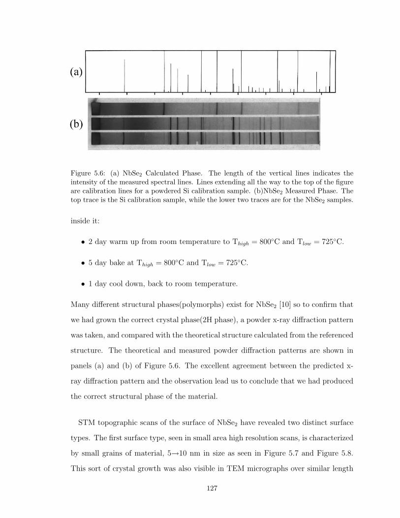
Figure 5.6: (a) NbSe2 Calculated Phase. The length of the vertical lines indicates theintensity of the measured spectral lines. Lines extending all the way to the top of the figureare calibration lines for a powdered Si calibration sample. (b)NbSe2 Measured Phase. Thetop trace is the Si calibration sample, while the lower two traces are for the NbSe2 samples.
inside it:
• 2 day warm up from room temperature to Thigh = 800C and Tlow = 725C.
• 5 day bake at Thigh = 800C and Tlow = 725C.
• 1 day cool down, back to room temperature.
Many different structural phases(polymorphs) exist for NbSe2 [10] so to confirm that
we had grown the correct crystal phase(2H phase), a powder x-ray diffraction pattern
was taken, and compared with the theoretical structure calculated from the referenced
structure. The theoretical and measured powder diffraction patterns are shown in
panels (a) and (b) of Figure 5.6. The excellent agreement between the predicted x-
ray diffraction pattern and the observation lead us to conclude that we had produced
the correct structural phase of the material.
STM topographic scans of the surface of NbSe2 have revealed two distinct surface
types. The first surface type, seen in small area high resolution scans, is characterized
by small grains of material, 5→10 nm in size as seen in Figure 5.7 and Figure 5.8.
This sort of crystal growth was also visible in TEM micrographs over similar length
127

Figure 5.7: 40 nm by 40 nm, z range 1.1 nm scan of an NbSe2 surface at room temperature.Tunneling was performed at 30 mV bias voltage, 0.5 nA tunneling current.
scales. TEM electron diffraction revealed that these grains are monocrystalline. The
surface structure observed in these figures was seen in a minority of the NbSe2 samples
studied.
The majority of surface topographies bore a stronger resemblance to that shown
in Figure 5.9. In NbSe2, intralayer forces between atoms are at least 100× greater
than interlayer forces. This results in a material which can be easily peeled, exposing
clean inert surfaces ideal for STM study. These last figures show the freshly peeled
plane structure expected for NbSe2.
128

Figure 5.8: 80 nm by 80 nm, z range 2.9 nm scan of an NbSe2 surface at room temperature.Tunneling was performed at 30 mV bias voltage, 0.5 nA tunneling current.
129

165 nm by 165 nm, z range 5.35 nm1.00 V at 100 pA
Figure 5.9: Terraced surface of NbSe2 showing 4 Asteps. Step edges appear bright due toovershoot in the feedback system.
130

In addition to topography on NbSe2 we are also interested in performing I/V and
I/Z spectroscopy. I/V spectroscopy both above and below the transition temperature
should show marked differences due to superconductivity. Below TC=7.2 K for NbSe2
a δ = 1.1 meV energy gap begins to open which can be imaged using I/V spectroscopy.
In addition to the 1.1 meV gap, a ±34 mV charge density wave discontinuity is present
below ≈ 33K. Figure 5.10 shows 3 preliminary spectroscopic scans of the same NbSe2
surface. If one were tunneling with a metallic tip into a metallic sample, the ∂I∂V
scans
would appear as straight horizontal lines in this figure. The sharp dip in conductivity
at 0 V bias is due to the formation of Cooper pairs at the Fermi energy, suppressing
the density of states. The overall parabolic shape of each curve is due to the charge
density wave state. Close examination of the width of the gap in Figure 5.10 reveals
that the width is 4.4 meV. The width of the gap in Figure 5.10 should be 2∆ = 2.2
meV but the observed width is twice that value. This can be explained if one suspects
that the STM tip has become contaminated with NbSe2, which is quite possible in
this instance as the STM tip did crash before this I/V scan was taken. Further I/V
scans will be required to understand whether the ripple oscillations in Figure 5.10 are
real or an artifact. I/V measurements taken as the sample temperature rose above
TC lacked the superconducting gap structure shown here.
Whenever spatial and spectroscopic images are acquired using STM it is necessary
to assess the conditions of tunneling by performing I/Z spectroscopy and measuring
the effective work function of the tunnel barrier. Figure 5.11 shows a typical I/Z spec-
tra acquired while tunneling into NbSe2 at liquid helium temperatures. Fitting the
current in Figure 5.11 with an exponentially decaying function allows us to calculate
the effective work function φ from the decay constant. If the exponential fit is of the
form I = I0e−2κz where I0 is the initial current, z is the tip height and κ is the decay
constant. Then the work function φ can be related to κ by:
131

0.00
0.25
0.50
0.75
1.00
1.25
1.50
-25 -20 -15 -10 -5 0 5 10 15 20 25Bias Voltage(mV)
Dif
fere
ntia
lCo
ndu
ctan
ce(a
rbun
its)
0.00
0.25
0.50
0.75
1.00
1.25
1.50
-25 -20 -15 -10 -5 0 5 10 15 20 25Bias Voltage(mV)
Dif
fere
ntia
lCo
ndu
ctan
ce(a
rbun
its)
0.00
0.25
0.50
0.75
1.00
1.25
1.50
-25 -20 -15 -10 -5 0 5 10 15 20 25Bias Voltage(mV)
Diff
eren
tialC
ond
ucta
nce(
arb
unit
s)
Figure 5.10: 3 separate spectroscopic scans of the differential conductance of NbSe2 overthe range of ±25 meV.
132

I/Z tunneling into Niobium Diselenide at 4.2 K
0.0
0.1
0.2
0.3
0.4
0.5
0.6
0.7
0.0 1.0 2.0 3.0Tip Displacement(Å)
Tu
nn
elin
gC
urr
ent(
nA
)
I/Z data
Exponential fit for an effectiveworkfunction of 2.5 eV
Figure 5.11: I/Z tunneling into niobium diselenide at 4.2 K
κ = 0.51√φ(eV )A−1 (5.2)
Using this equation gives a value for φ = 2.5 eV tunneling into NbSe2, comparable to
the 2 eV work function measured by Hess [1].
The preliminary results presented here are part of an ongoing effort to first repro-
duce some of the static vortex imaging results of Hess et al. [1] as an initial step in
investigations into time-resolved vortex dynamics. An experimental proposal to do
133

will now be briefly outlined. STM tunneling between a metallic tip and a supercon-
ducting NbSe2 sample will be established. The NbSe2 sample will be mounted on the
STM sample sled, shown in Figure 5.2. Beneath the sample a 1.2 Tesla neodymiumn
iron boron magnet will create the vortex state in the NbSe2 sample once it is cooled
below TC=7.2 K. The spacing between vortex cores is expected to be 489 A/B1/2
or 53.6 nm [11]. Imaging the vortex state will be one of the primary steps in the
experiment. Another primary step is to determine whether Ti/Sapph illumination of
the NbSe2 surface affects its superconductivity as observed by Testardi [12] in thin
Pb films. Testardi observed local heating of electrons above the lattice temperature
which suppressed superconductivity in Pb. Optically heating electrons above TC in
our NbSe2 samples will be the pump in the pump/probe experiment. It may be
possible to observe an effect in the DC I/V spectra, but by junction mixing STM it
should be possible to directly image the I/V spectra as a laser pulse is incident on the
tunnel junction and time-resolve the evolution of the LDOS from a superconducting
state to a normal (hot electron) state and back to a superconducting state as the
electron heat is transferred to the NbSe2 lattice. By combining lattice imaging, with
the time-resolved evolution of the LDOS, due to optical pumping the NbSe2 surface,
we will attempt to image the evolution of the vortex state due to optical pumping.
The surface vortex state should vanish as hot electrons are produced on the surface
due to optical pumping but the bulk vortex state should remain allowing vortices to
reform in their same positions on the superconducting surface once the electrons have
cooled and the surface state is restored.
To this point our attempts to image the vortex structure of NbSe2 have met with
limited success. Initially vibration isolation and electrical requirements have necessi-
tated multiple redesigns of the microscope in an attempt to achieve stable low tem-
perature STM tunneling into our samples. The latest efforts with an STM immersed
in liquid helium were hampered by the nucleation of helium bubbles on the surfaces of
134
the STM along with the unfortunate gettering of solid oxygen onto our sample surface
and magnetic damping mechanisms. These problems have lead to the recent devel-
opment of a high vacuum low temperature microscope which should eliminate the
present experimental barriers. Other concerns for low temperature tunneling include
the risk of condensation forming on the samples of interest as they are cooled.
To surmount this obstacle, experiments have begun to laser ablate our sample
surfaces in situ at low temperatures. Results of such a laser ablation can be seen
by comparing the surface shown in Figure 5.12 that of Figure 5.13. The stark
contrast between the surfaces before and after the laser pulse suggests a large amount
of original surface has been removed, exposing a clean contaminant-free surface. This
has not yet been confirmed as the present experiments were performed in ambient
conditions and no change in the surface work function was observed.
Another factor which has hindered recent progress has been in the slow turn around
times of the microscope when STM tips perform poorly. Currently STM tips are
purchased commercially to ensure consistency. Once a tip is mounted into the micro-
scope, the microscope is evacuated and cooled, a time consuming process, and then
tunneling is attempted. If the tip is not in excellent condition it must be replaced.
The warm up time for the microscope is quite long and many hours must pass before
another tunneling attempt can be made. Recently however a new room temperature
STM was purchased with the goal of allowing us to characterize our STM tips before
they are mounted in the low temperature microscope. With this pre-characterization
we hope to reduce the number of unsuccessful microscope cool downs increasing our
tunneling efficiency.
A great deal of effort has gone into the design and construction of a high vacuum low
temperature scanning tunneling microscope. The vibration isolation system consists
of 4 stages, a stable sand based mount, supporting a pneumatic isolation system which
135

50.9 nm by 50.9 nm, z range 8.85 nm49.8 mV at 1.90 nA
Figure 5.12: NbSe2 surface with hole in the corner of the image. Small depressions in theflat plane topography are 4Adeep.
136

50.9 nm by 50.9 nm, z range 40.1 nm49.8 mV at 1.83 nA
Figure 5.13: The same NbSe2 sample shown in Figure 5.12 after focused illumination witha 20 mJ Excimer 308 nm laser pulse.
137

itself supports a series of stacked steel plates. Hanging from this on stainless steel
springs rests the microscope itself. This isolation system is sufficient in isolating our
microscope from the mechanical vibrations of the building and the bubbling action
of the cryostat. The electronics of the microscope have been carefully designed to
eliminate and shield all sources of noise and cross talk which might interfere with
the delicate current measurements which STM requires. The performance of the
microscope has been continually improved over a number of years to the point that
atomic scale resolution has been achieved and sub meV spectroscopic resolution has
also been demonstrated. It is unclear how close the current system is to being able to
make the vortex imaging measurements we would like. All indications suggest that
this should be achievable with the latest microscope which has been developed. Past
experiences warrant cautious optimism that such measurements can be made in the
not too distant future.
References
[1] H. F. Hess, R. B. Robinson, R. C. Dynes, J. M. Valles, Jr., and J. V. Waszczak.
Phys. Rev. Lett., 62:214, 1989.
[2] A. Dhirani, A. J. Fisher, and P. Guyot-Sionnest. Rev. Sci. Instrum., 67:2953,
1996.
[3] K. Nagaya. Transactions of the ASME: J. Dynam. Syst. Meas. Control., 106:52,
1984.
[4] C. Julian Chen. Introduction to Scanning Tunneling Microscopy. Oxford Uni-
versity Press, New York, 1993.
[5] Henry W. Ott. Noise Reduction Techniques in Electronic Systems. John Wiley
& Sons, New York, 1976.
138

[6] Ralph Morrison. Grounding and Shielding Techniques in Instrumentation. John
Wiley & Sons, New York, 1967.
[7] R. Kershaw, M. Vlasse, and A. Wold. Inorg. Chem., 6(8):1599, 1967.
[8] R. M. A. Lieth, editor. Preparation and Crystal Growth of Materials with Lay-
ered Structures, volume 1 of Physics and Chemistry of Materials with Layered
Structures. D. Reidel Publishing Company, Boston-U.S.A., 1977.
[9] Antony R. West. Solid State Chemistry and its Applications. Wiley, New York,
1984.
[10] F. Kadijk and F. Jellinek. J. Less-Common Metals, 23:437, 1971.
[11] H. F. Hess, R. B. Robinson, R. C. Dynes, J. M. Valles, Jr., and J. V. Waszczak.
J. Vac. Sci. Technol. A, 8(1):450, 1990.
[12] L. R. Testardi. Physical Review B, 4(7):2189, 1971.
139

Chapter 6
Conclusions
Driven by the desire to study ultrafast phenomena on nanometer length scales
several proposals were made to develop time-resolved scanning tunneling microscopy.
The three most significant of these were the photo-gated STM approach of Weiss et
al. [1] and Takeuchi and Kasahara [2], the distance modulation technique of Freeman
and Nunes [3] and the junction mixing technique developed by the same authors [4].
PG-STM boasted excellent time and spatial resolution, but the basis for these
claims was not sound. Citing vertical sensitivity as a measure of spatial resolution is
misleading and it was later discovered that the time-resolved signal from the PG-STM
was capacitively coupled from sample to tip [5]. This led to the conclusion that the
true spatial resolution of PG-STM would be hundreds of nanometers at best.
Distance modulated STM does not have such limitations. Rapid changes in tip/sample
separation are used to demodulate the fast response of a sample under investigation.
This technique is quite general in its applications. So long as one can excite a sample
repetitively such that the excitation can be detected by the STM the distance mod-
ulation technique should work. Transmission lines launching electrical pulses at the
tunnel junction are not required. What is required is that the tip of the STM can
be physically moved on very fast time scales. This technique has been demonstrated
up to nanosecond time scales, but if faster time-resolution is required the distance
140

modulation technique will not suffice.
Junction mixing STM is suited for situations where ultrafast time resolution is
required. This method for time-resolved STM employs no moving parts, instead rely-
ing on the non-linear electrical properties of the STM tunnel junction to demodulate
ultra-fast sample response. For this technique to work an electrical probe pulse must
be launched into the tunnel junction of the STM. The pulse may be launched from the
STM tip or from a sample giving JM-STM flexibility to study samples non-invasively.
Working to develop JM-STM, three key experiments were presented in this thesis.
The first work used a lithographically patterned transmission line structure to launch
two electrical pulses into the tunnel junction. These pulses were successfully detected
by the STM as it tunneled into the transmission line. The detection of a 10 ps time-
resolved signal marked an order of magnitude improvement over previous JM-STM
experiments [4]. By launching electrical pulses from either side of the STM tip this
experiment was the first to confirm that non-linearities in the tunnel junction were
the only source for this signal.
A direct demonstration of combined spatio-temporal resolution was the last hurdle
in establishing JM-STM. By patterning an array of small titanium dots onto a trans-
mission line structure combined spatio-temporal resolution could be demonstrated.
Titanium provides I/V contrast with the gold of the transmission line, so the time-
resolved signal will vary as the STM scans across the titanium gold interface(the
edge of a titanium dot). Varying pump/probe delay times allowed an electrical probe
pulse to sample the pumped transmission line sample. At every pump/probe interval
an STM spatial and time-resolved scan was taken, creating the first ultrafast STM
movie.
141

To confirm the interpretation of previous results and explore the limitation of the
JM-STM technique a lumped element model was developed. Fits from this model to
experiment contained only one fitting parameter, the size of the voltage pulses on the
transmission line. Using this fitting parameter we find excellent agreement between
the model and experimental data 1. Extrapolating results from the model allows the
prediction that JM-STM can be extended into the femtosecond time regime, limited
by the geometrical tip/sample capacitance.
To demonstrate JM-STM on a physically interesting system a low temperature
high vacuum STM was developed. This microscope provides the optical access and
electrical connections required for JM-STM. Mechanical vibration isolation was met
by hanging the microscope into a liquid helium dewar without allowing dewar vibra-
tions to couple to the microscope. A high vacuum environment was provided using
a turbo-pump backed by a dry scroll pump. Using this microscope I/V spectroscopy
on NbSe2 has revealed superconducting gap structure.
By combining our newly developed high vacuum low temperature STM with our
reliable Ti/Sapph laser system, investigations into nonequilibrium superconductivity
on NbSe2 are poised to commence.
References
[1] S. Weiss, D. F. Ogletree, D. Botkin, M. Salmeron, and D. S. Chemla. Appl. Phys.
Lett., 63:2567, 1993.
[2] K. Takeuchi and Y. Kasahara. Appl. Phys. Lett., 63:3548, 1993.
[3] M. R. Freeman and Geoff Nunes, Jr. Appl. Phys. Lett., 63:2633, 1993.
[4] Geoff Nunes, Jr. and M. R. Freeman. Science, 262:1029, 1993.1it should be noted that voltage pulse magnitudes agreed well with our estimates
142

[5] R.H.M. Groeneveld and H. van Kempen. Appl. Phys. Lett., 69:2294, 1996.
143

Appendix A
Junction Mixing STM ControlSoftware
A.1 Introduction
In order to control the microscopes used in this research it was necessary to write
a great deal of controlling software. Software was required which would monitor and
control the STM sample approach, scanning functions, spectroscopy functions and
analysis. LabView was chosen as the development environment due to its ease of use
and its rapid application development time.
LabView is an object oriented graphical programming environment which consist-
s of modules, control structures and wiring to connect modules together. Modules
are basically subroutines with a discrete number of input and output ports. Module
input/output types are numerous, consisting of numerical, boolean and string con-
stants or arrays. One of the strengths of LabView lies in the vast library of available
modules and the simplicity with which they can be connected together. Connections
between modules is accomplished through LabView’s wiring tool. Wiring is typically
made between the output of one module to the input of another. This is only possible
if the output and input share a common data type you could not wire a boolean array
to a string input, only to another boolean array). To control the order and frequency
with which modules are executed, LabView includes a basic set of control structures.
In order to repeat an operation n times one could simply encircle the appropriate
modules with a for loop. To do this you literally just drag a for loop over the modules
and wire the number n to the input of the loop. LabView’s control structures include
for loops, sequence structures, while loops and case structures.
144

As one might expect for a development environment LabView includes extensive
debugging features and profiling tools. Setting break points, pause points and a ‘visual
execution’ mode showing program execution in slow motion along with the values
passed from module to module are all features which simplify debugging. Profiling
tools allow the user to time how long it takes for any given module or section of
modules to execute. This execution time typically results from a combination of
processing time, operating system time (where the operating system interrupts the
operation of LabView to perform other tasks) and I/O time where LabView is sending
or receiving data from a data acquisition card for example.
Data acquisition and experimental control functions are the best applications for
LabView programs. LabView contains pre-built modules specifically designed for
interfacing with data acquisition cards. This eliminates the need for the end user
to learn the technical details of the specific data acquisition device. Using pre-built
data acquisition modules a user could be sending and receiving data from computer to
data acquisition card (DAQ) in mere minutes. Since these DAQ modules can be easily
linked to other LabView modules such as a 2D-graphing module one could capture
and plot 2D data in a very simple LabView program containing just 2 modules wired
together. By adding one more module to output data to a digital to analog(DAC)
converter one could create a simple scanning program which outputs voltages to
control an actuator’s position while simultaneously reading transducer values and
plotting the values on a computer screen. All this with just 3 modules and about 2
minutes of programming!
Due to its ease of use LabView was chosen as the programming environment for
developing the control and data acquisition tools for our STMs. There are 4 basic
functions associated with a TR-STM system for which control programs were devel-
oped:
• STM sample approach
• STM topographic scanning
• STM I/V and I/Z spectroscopy scanning
• Optical delay line scanning
Details of each of these programs will now be addressed.
145

A.2 STM sample approach
In a typical STM system there are two approach mechanisms to bring the tip
of the microscope into tunneling distance with the surface to be investigated. A
coarse approach mechanism will bring the tip of the microscope close enough to the
sample that the fine approach mechanism can establish tunneling. Coarse approach
mechanisms used in this work include a stepper motor based approach and a linear
stick slip approach. In the stepper motor approach a stepper motor is connected
to a screw which drives the STM tip into the sample. The motion of the screw is
de-amplified so that discrete motor steps are on the order of 8 nm. The coarse linear
stick slip approach uses a 3 piezo tube base, which the sample rests on. By applying
a slowly increasing voltage to the base piezo’s the sample can be moved towards the
tip. By rapidly reducing the applied voltage back to zero the piezo’s will snap back
to their initial position, but the sample will remain fixed. This is accomplished since
the kinetic friction between the sample and base as the piezo’s are snapped back, is
less than the static friction between sample and piezo’s as the sample is moved slowly
forward. In both microscopes used in this work, the same fine approach mechanism
is used. A five electrode piezo is used for fine tip/sample approach. The outer four
electrodes control tip x/y deflection while the central z electrode controls the tip
height above the sample.
The complete approach is accomplished as follows. A negative voltage is applied
to the z electrode of the piezo tube to retract the tip. The coarse approach the
moves the sample and tip one step closer together. If the tip has not encountered
the surface the piezo tube is slowly extended up to its full length in an attempt to
establish tunneling. This sequence is iterated until tip and sample are close enough
that a measurable current is found.
Two main programs are used to control the STM tip approach. The first program
found in the Gms.llb library is called ‘Tip Approach’ and is used to control the stepper
motor approach of the room temperature STM. The front panel(user interface screen)
of ‘Tip Approach’ is shown in Figure A.1. The functions of the controls on the front
panel will now be outlined. For the program to run the ‘On’ switch must be in the
up position. Once the program is running the stepper motor will advance in either
the up or down direction by either a half or full step increment. For clarity up and
down refer to the direction the screw attached to the stepper motor will move. If
the ‘Windings are On’ button is not engaged the stepper motor will not move and
146

Figure A.1: User interface for the program ‘Tip Approach’ used to control the room tem-perature STM stepper motor approach.
147

the screw can be adjusted by hand. The piezo ‘Step Size’ is the increment in volts
between 5 mV and 20 V that is used to move the piezo towards the surface after a
coarse motor step is made. Initially the piezo will be fully retracted(at -10 V) and the
motor will advance one step. Then the piezo will be incremented from -10 V to 10 V
in ‘Step Size’ voltage increments. The motor coarse approach and piezo fine approach
will continue until a voltage is read which is within the ‘Acceptable Deviation’ of the
‘Threshold Voltage’. In typical STM scans a current of .5 nA was used, with a bias
voltage of 50 mV a current pre-amp gain of 108 V/A. The homebuilt IBM feedback
controller feedback set point is set to 4.24. When proper tunneling is established the
current voltage converter would give a voltage of 50 mV and the ‘Threshold Voltage’
used for the approach is 5 V with an ‘Acceptable Deviation’ of 4.98 V. Under these
circumstances any voltage above 20 mV will trigger the approach to stop. It should
also be noted that the program takes the absolute value of the measured voltage so
that the approach works with either positive or negative bias voltage polarity. If the
tip does crash into the surface and the user wants to withdraw it quickly on can
simply reverse the motor step direction, set the ‘Threshold Voltage’ to zero and the
‘Acceptable Deviation’ to 20 mV to pull the tip out of a crashed condition. Another
idiosyncrasy to note is that if the piezo ‘Step Size’ is set to zero the piezo will not
be stepped during the approach. This will speed up the tip approach immensely and
is not a problem so long as the range of the STM feedback system is larger than
the motor step size(STM feedback range can be increased by simply amplifying the
output of the feedback controller using the high voltage power supply).
The approach program described above operates for the room temperature STM
using a stepper motor as the coarse approach mechanism. The next program discussed
is designed for the low temperature STM and controls a stick slip coarse approach.
The front panel of ‘Fast approach 1.1’, found in the STM2 lib.llb library is shown in
Figure A.2. The basic function of this program is to output a sawtooth waveform
to drive the base piezo’s such that the sample(resting on the base piezo’s) will be
ratcheted towards the sample. The ‘Direction’ switch controls the polarity of the
voltage pulse. The pulse is output to both channels 0 and 1 of the DAQ and the
polarity of output 0 is opposite that of channel 1. These voltages are applied to the
front and back surfaces of the piezo’s respectively. The amplitude of the sawtooth
waveform is controlled by the ‘Pulse Voltage’ control and the ‘Approach Mode’ control
sets the number of discrete steps in the rising edge of the waveform. The update rate
sets the number of DAQ updates per second and should be set to 20 kHz. The
‘Iterations’ indicator keeps track of the total number of steps made in the approach.
148

Figure A.2: User interface for the program ‘Fast approach 1.1’ used to control the lowtemperature STM stick slip approach.
149

The ‘Voltage Set Point’ and ‘Margin’ behave in the same way that they did in the
‘Tip Approach’ program. When the sample is approaching in this way capacitive
coupling in the STM wiring can often led to pickup on the STM tip line. This
pickup is amplified in the current to voltage converter and can trigger the approach
mechanism to halt an approach. To compensate for this once the approach mechanism
is stopped the tip voltage is again checked with respect to the ‘Voltage Set Point’. If
the voltage is not within the ‘Margin’ to the ‘Voltage Set Point’ then the approach is
resumed and a ‘False Read’ is indicated in the indicator box. Once the tip approach
has completed and the STM is tunneling it might be necessary to do single step
coarse adjustments to the sample position. These can be accomplished by using the
‘Manual Approach 1.1’ program found in the STM2 lib.llb library. The front panel
for this program is shown in Figure A.3. With this program the user can step the
STM sample a single step towards or away from the tip using the inner left and right
buttons in the ‘Manual Approach Control Cluster’(pressing one of these buttons will
send one sawtooth wave and move the sample by one increment. The outer left
and right buttons can be held down to step the sample continuously in the desired
direction. The scanner voltage control can be used to adjust the tip position. The
‘Pulse Characteristics’ cluster allows the user to adjust the shape and speed of the
waveform(these settings should not have to be adjusted).
A.3 STM topographic scanning
Once the STM sample has been moved to within tunneling distance of the sample
the user may want to perform topographic scans of the samples surface. In order to
accomplish this the STM feedback, bias and high voltage electronics are configured so
that the a fixed bias voltage is applied to the sample, the feedback electronics output a
voltage to the high voltage supply which is amplified and sent to the STM piezo’s such
that a constant current from the current pre-amp is maintained. This configuration
is known as constant current tunneling. If the tip of the microscope is moved over
the surface of the sample the feedback electronics adjusts the height of the tip so
that it remains a fixed height over the sample. By monitoring the feedback voltage
one can track the topography of the surface. A simple topographic scanning program
will simply raster scan the STM tip through a grid of positions over the surface.
At each grid point the scanning program will input the feedback voltage signal in
order to build a topographic image of the surface. Two STM scanning programs have
been devolved for use with the room temperature and low temperature STMs. The
properties of the two programs and their operation will now be discussed.
150

Figure A.3: User interface for the program ‘Manual approach 1.1’ used to step the lowtemperature STM stick slip approach.
151

The first scanning program to be discussed is called ‘STM Scan w/N-Regression
v3.4’ found in the STM2 lib.llb library. The front panel of this program is shown
in Figure A.4. The first controls to look at when setting up a scan are the primary
and secondary scan amplitudes. These can be set between 0 V and 10 V and will
set the amplitude of a bipolar scan. So a primary scan amplitude of 0.42 V will scan
the tip in the primary direction over a voltage range of -0.42 V → 0.42 V. So long
as the primary and secondary scan amplitudes are the same the topographic scan
will be square but the user can set the secondary scan amplitude to whatever value
is desired; zero for example will cause the controller to perform a line scan over the
surface. Primary and secondary scan points control the grid spacing of points over
the primary and secondary voltage ranges. Forward and backward delay times set
how long the tip waits at each grid point before acquiring data in the forward and
back, scan direction1. The X Offset and Y Offset controls are currently disabled.
Currently this program allows the user to acquire up to 4 input values for every
scan point in the forward scan direction and up to one input for the backwards scan
direction. Acquiring data in the backward scan direction is useful in identifying AC
pickup, examining piezo hysteresis and looking for true topography. AC pickup will
often appear as tilted stripes through an STM image but the tilt of these stripes will
be reverse in the backscan image. Piezo hysteresis will appear at the edges of the
forward and back scans where the STM tip is being forced to change direction. True
topographic images should look almost identical in the forward and back direction,
but it must also be noted that any tip asymmetry(topographic or electrical) can cause
image distortion between forward and back-scanned images. In a typical scan both
STM tunneling current and feedback voltage will be monitored in the forward scan
direction and feedback voltage can be monitored in the back scanning direction.
A unique feature of this scanning program is its ability to compensate for large
variations in surface topography and nonlinearities in piezo response. This allows
very large images to be taken, images up to 5µm2. This is accomplished by fitting
the scanned surface with a set offset, a plane or an nth order polynomial of x and
y. After a surface is scanned it can be fit with any one of these surfaces, where
the surface type would be chosen to compensate for sample tilt or the parabolic
behavior of the scanning piezo when scanned over large distances. After the surface1When a scan begins, the tip is moved to the bottom/left quadrant of the scan area. It then scans one
line forward, then back in the primary scan direction. It then increments in the secondary scan directionand does the next scan in the primary direction. This process it iterated until the scan is complete andthe tip is in the upper/left quadrant of the scan range. Finally the tip is restored to the center of the scanrange(0 V on the primary and secondary outputs).
152

Figure A.4: User interface for the program ‘STM Scan w/N-Regression v3.4’ used for largeslow STM scans.
153

is scanned and fit the fit parameters are displayed in the ‘Measured Coeffs’ box on
the user interface. If these parameters are copied and pasted into the ‘Coeffs’ box
directly above the measured values, the following surface scan will include an output
compensating voltage to the z piezo so that the piezo will be adjusted for sample tilt
and the natural parabolic motion of the tip. In this way we greatly reduce the feedback
voltage range required to do large area surface scans. The ‘Measured Coefficients’ are
effectively dimensionless, so that once they have been measured for a set scan range
and scan points, one can change both these values and still scan along the same plane
or surface. In practice one could scan a relatively small area, say 100 nm2, calculate
the sample tilt and then start scanning larger and larger areas adjusting the fitting
parameters as the scan range is increased. A second order polynomial fit is suitable
for large area scans.
In order to take advantage of the tilt and piezo compensation the scanning program
must have access to 3 digital to analog output channels. Typical National Instruments
DAQs(data acquisition cards) have only 2 analog outputs so 2 DAQs were used with
this program. In order to synchronize outputs between the two boards a simple
LabView module was used which updates the voltage value of each analog output
sequentially one after another. This ensures that each channel is updated before each
measured input value is taken. The disadvantage of this process is that scans are
quite slow to acquire(taking about 2 minutes for a 128x128 point scan). Due to these
concerns the program ‘STM Scan w/N-Regression v3.4’ should only be used where
slow scans are acceptable and large scan areas are required. These two parameters
don’t really conflict though, since for large scans the tip velocity over the surface is
quite large and should be limited to within the bandwidth of the feedback system.
So for large scans, slow scans are in fact necessary(2 minutes for a 128x128 scan
on the order of 1µm2 is quite reasonable). When scanning small areas looking for
atomic resolution it can be necessary to scan very quickly to minimize thermal drift.
For small scan areas it is not that important to compensate for surface tilt or the
parabolic motion of the piezo scan tube as the angular variation of the piezo tube is
minimal. To optimize small area scanning, another scan program was developed.
‘Scan Executioner 2.0’ found in the STM2 lib.llb library was developed for small
area fast scans. The user interface for this program is shown in Figure A.5 Examining
the user interface for the Scan Executioner program a few differences will stand out.
First is the ‘Rate’ control which sets the speed with which scan channels are up-
dated. The value 1000 is the maximum setting for this control and corresponds to
154

Figure A.5: User interface for the program ‘Scan Executioner 2.0’ used for small fast STMscans.
1000 updates per seconds2 giving 128x128 scan times of about 30 seconds. The way
Scan Executioner works is in fact quite different from the previously discussed STM
scan program. First the user input the desired scan range and scan steps, then the
Scan Executioner passes these values to a subroutine called Scan Matrix Generator.
This program generates the entire matrix of voltages to be scanned over and passes
them back to the Scan Executioner. The matrix is then passed to the Scan Initia-
tor subroutine. This subroutine loads the matrix into memory(through DMA) on
the DAQ and programs the DAQ to output matrix values while concurrently taking
input values at the desired ‘Rate’. The DAQ then begins executing at a rate inde-
pendent of operating system interrupts and other OS functions. In this way the DAQ
acquires data in real time. Once the input data has been gathered it is passed back
to the PC(via DMA) and into the scan executioner program where it is displayed in
Graph 1. When the data is displayed it is wise to check the length of the data array
versus the ‘Expected Points’ indicator just to check that all the data got through .
The scanner scans forward and backward each line in x before it increments y. All
the raw data is shown in Graph 1 and simultaneously parsed into Intensity Graph 1
and Intensity Graph 23.2since 2 channels are being updated for every point in the scan this corresponds to about 2 ms per point.3The Data in Intensity Graph 2 has been reversed so that the positive x direction in both intensity graphs
is the same.
155

Another feature in this scanning program which aids in scanning small features is
the variable gain control over analog input. Input gain is adjusted by changing the
input range from ±10 V to ±50 mV. Unfortunately there is no such gain control for
output voltages and one must take care to ensure the voltage step size being output
is not too small. The maximum output range of the 12 bit DAC(digital to analog
converter) is ±10 V, which gives a minimum output voltage increment of 4.88 mV.
It is always a good idea to check the value of the ‘X Step Size(mV)’ indicator, since
it should ideally be an integral multiple of 4.88 mV so that the x voltage increments
the same amount with every scan point. Under special circumstances it might be
desirable to scan without the feedback on so there is a control on the front panel to
allow this. If saving data, curve fitting or other types of analysis are desired one can
enable the ‘Launch Scan Analyzer?’ button which will pass the acquired data to the
next important scanning program.
‘Scan Analyzer 2.0’ can be found in the STM2 lib.llb library and is shown in Fig-
ure A.6 Scan Analyzer allows a few useful data fitting choices, line by line fitting
where the slope of each line of data is adjusted to zero is useful for small scans at
room temperature where constant thermal drift can mask out small topographic vari-
ations such as atomic corrugations. Line by line fitting will occur if the ‘Line by Line
fit’ button is depressed. Polynomial surface subtraction of any order(order is set by
the ‘Degree of Polynomial Fit’ button) can also be performed simply by pressing the
‘Poly Subtract’ button for the appropriate data channel. If neither button is pressed
then the raw data will appear in the ‘Forward Fit Data’ graph. The raw data as taken
from the Scan Executioner program is shown in the ‘Data Array’ graph and a Fouri-
er transform of this data is shown in the ‘Fourier Transform of Data Array’ graph.
It should be noted that this Fourier transform will include the scan rate frequency
and all its Fourier component. The Fourier transform will often aid in eliminating
noise sources from the STM signal4. In addition to surface topographic scans STMs
can probe sample LDOS through current voltage spectroscopy. They can also probe
surface contamination through current gap height spectroscopy.
A.4 STM I/V and I/Z spectroscopic scanning
The primary controlling program used for these scan types is ‘I / (V or Z) Curve 3.1’
found in the STM2 lib.llb library and shown in FigureA.7. This program operates in4The LabView program Spectrum Analyzer 3 0.vi can be used to get real time Fourier analysis of the
STM current or any other signal of interest
156

Figure A.6: User interface for the program ‘Scan Analyzer 2.0’ used to save and fit dataacquired through ‘Scan Executioner 2.0’.
157
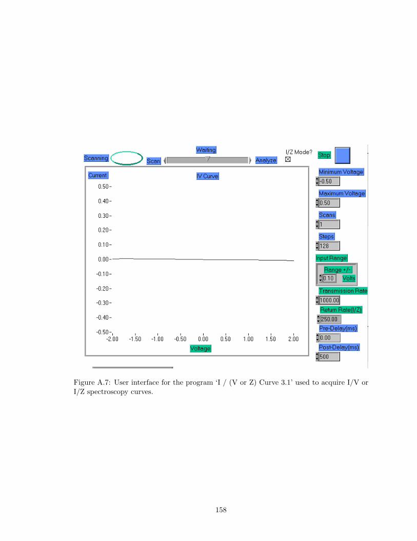
Figure A.7: User interface for the program ‘I / (V or Z) Curve 3.1’ used to acquire I/V orI/Z spectroscopy curves.
158
the same manner as the Scan Executioner program. A scan matrix is set using the
‘Minimum Voltage’ and ‘Maximum Voltage’ controls, and the ‘Steps’ control. Input
gain can be adjusted using the ‘Input Range’ selector. Scan rate can be set for both
the forward and backward scanning directions, using the ‘Transmission Rate’ and
‘Return Rate’ controls. This program is capable of performing individual scan but
if more scans are required(due to signal noise) multiple scans can be taken and are
averaged automatically. While these scans are being taken the STM feedback system
is disabled through a TTL digital I/O line. If ‘I/Z Mode’ is selected the feedback
system will be enabled after the I/Z scan has withdrawn the tip. The tip will then be
returned to its initial position with the feedback active, to avoid tip crashes due to
thermal drift. After a good scan has been captured, clicking on the ‘Analyze’ slider
will cause the program ‘I / (V or Z) Analyzer 2.0’ found to be launched.
Shown in Figure A.8 ‘I / (V or Z) Analyzer 2.0’ is capable of fitting curves with lin-
ear, polynomial or exponential curves in order to analyze sample electrical properties
and tunneling conditions such as the effective tunneling work function. This program
also allows I/V or I/Z data to be saved. Operation of this program is quite simple,
one simply selects the desired polynomial order or exponential polarity(whether the
current values are positive or negative) and then click on the ‘Polynomial’ or ‘Ex-
ponential’ slide bar positions. Once a fit is suitable click on the ‘On’/off switch to
stop the program, prompting the user to save the data. The program can always be
restarted to re-fit the data. The range of data to be fit can also be adjusted through
the ‘Fit Range’ control.
A.5 Optical delay line scanning
The last piece of STM control software to be discussed is the program which controls
the laser pulse delay in a time-resolved STM(TR-STM) experiment. In TR-STM
experiments an STM image will be acquired which typically includes topographic in-
formation, STM current over the scan, and the time-resolved STM signal as detected
by the lock-in amplifier. All this data will be taken for a given delay time(or retrore-
flector position) which will then be incremented to build a time-resolved movie. The
program which controls the movement of the optical delay line can be found in the
library STM2 lib.llb and is called ‘Motor Control 2.0’ shown in Figure A.9. Inputs
for this program are given in terms of stepper motor increments and the delay time
between increments. It is often more convenient to think in terms of delay times, so
a little program called ‘Scan Calculator’ is run in conjunction with the motor con-
159

Figure A.8: User interface for the program ‘I / (V or Z) Analyzer 2.0’ used to fit I/V orI/Z spectroscopy curves.
trol program. ‘Scan Calculator’ also shown in Figure A.9 allows one to simply input
the start and stop delay times for the scan, it then calculates the appropriate motor
starting point in steps, and the increment interval. It was found that this program
yields the best results if all scans are taken in the same direction. In order to com-
pensate for any mechanical backlash, the ‘Roll Back’ control can be set to pretension
the delay line translation stage to minimize slop between scans. ‘Motor Control 2.0’
uses a simple data file called
c:\motor.dat
to keep track of the position of the stepper motor. Care must be taken to ensure that
the stepper motor is never asked to move the retroreflector past its mechanical limits.
There are currently no safeguards to prevent this. There are three modes which this
program runs in. The modes, set in the ‘Increment Options’ control are:
• Take Data Point
• Take Data Point and Pause
• Pause
These options control what the program does after moving the retro one set of in-
crements. If the program is caused to pause, a subroutine is launched which waits
for user intervention to continue. This is so that an STM scan could be performed
while the delay is held fixed. The ‘Scan Info’ section on the user interface is simply a
160

Figure A.9: User interface for the program ‘Motor Control 2.0’ used to acquire time resolveddata and control the delay time between pump and probe optical pulses. The interface for‘Scan Calculator’ is also shown.
161

convenient way for the user to input details about the time resolved scan which will
be printed along with the scan results. It serves no functional purpose.
162

Appendix B
Junction Mixing STM OpticalSystems
B.1 The Ti/Sapphire Laser
In order to time-resolve the operation of a scanning tunneling microscope, optical
pump probe techniques were used. These techniques relied on fast(60 femtosecond)
laser pulses delivered at 87.7 MHz to electro-optic switches. In order to produce these
laser pulses a Titanium doped Sapphire(Ti/Sapph) laser was constructed. Optical
component layout, alignment and performance diagnostics will be detailed in the
following sections. Trouble shooting symptoms and known cures will also be outlined.
The pulsed output of a Ti/Sapph laser is a remarkable phenomena. Pumping
a Ti/Sapph laser with continuous green laser light can produce continuous lasing
or a single pulse propagating within the cavity. Even more remarkable is that the
transformation from continuous to pulsed operation can be accomplished with the
flick of a finger. Before it was first discovered there was general agreement that
Ti/Sapphire lasers could not self mode-lock. However the serendipitous discovery
of what was to be called “magic” mode-locking was published in 1991 [1]. After
this discovery, the group of Salin, Squire and Piche developed the theory of Kerr
induced self focusing [2]. To learn the physics of this feat, I would refer the reader
to the subject of Kerr lens mode locking or to texts such as “Ultrashort Laser Pulse
Phenomena” by Diels and Rudolph [3]. Here we will gloss over the physics with
a simplified model. The Ti/Sapph crystal can emit a broad range of wavelengths
anywhere from 680⇒ 1100 nm. The wavelengths which satisfy the condition that an
integer number of half-waves fit into the cavity form the longitudinal modes of the
cavity. In CW mode a fairly narrow set of longitudinal cavity modes dominate the
lasing, typically a band of modes a few nm wide centered around 800 nm. When an
163

optical power spike is introduced into the cavity something remarkable can happen.
When this noise spike passes through the Ti/Sapph crystal the strong electric field
interacts non-linearly with the crystal, modifying its index of refraction. This is Kerr
lensing or self focusing, and will increase the overlap of the lasing area with the pump
beam. This will increasing the stimulated emission of the crystal as the noise spike
passes through, increasing the amplitude of the spike. With every pass in the cavity
the amplitude of the noise spike will build as the self focusing effect channels more
energy into a small volume in the crystal. Soon this effect will completely deplete
the population inversion in the most active volume of the crystal. This leads to the
formation of a short pulse in the cavity and can decrease or eliminate the CW power
in the cavity. CW power can still propagate in the cavity if there are many transverse
CW modes so that the self focused spot on the crystal does not completely overlap
with the CW spot. Using an adjustable slit within the cavity allows one to kill any
remaining CW component in the pulsed Ti/Sapph beam.
The Ti/Sapph laser described here was built based on the design paper by Kapteyn
and Murnane [4] 1. Lasing is accomplished by creating a population inversion in
the Ti/Sapph crystal by optically pumping it with another laser. In this case a 5
Watt, Spectra Physics Millennia(at 532 nm wavelength) is used at 4.5 W power in
the TEM00 mode for normal operation. Note that the polarization of the Millennia
must be rotated from vertical to horizontal so that it will be oriented properly with
respect to the orientation of the Ti/Sapph crystal. Our efforts using argon-ion lasers
were never successful in producing a stable pulse Ti/Sapph output since there was
insufficient power in the TEM00 mode. Pumping at 5 W the Ti/Sapph gives an
output power of 800 mW continuous wave(CW) power(not pulsed). Mode locked,
one should be able to get from 400 → 500 mW pumping at 5W. Normal operation
has the pump power at 4.5 W and the Ti/Sapph pulsed output power at about 400
mW. Apart from the Ti/Sapph crystal and the slit the only other important parts
of the Ti/Sapph cavity are the end mirrors and a pair of prisms which are used to
compensate for group velocity dispersion within the cavity. A schematic of the cavity
used in the present experiment is shown in Figure B.1.
Alignment of the Ti/Sapph cavity was performed as outlined in reference [4]. The
speed with which one can align the laser from scratch is simply a matter of experience.
With experience one should be able to completely align the laser within the course of1In this paper the authors welcome people to contact them for updates of the document. Since they now
sell these lasers commercially it is unclear if this policy still holds.
164

Fused silica prisms
16
Ti:Sapphire Rod(0.015% doped)
Focusing mirrors
10% output coupler
Focusing lens for pump beam
Narrow slit
High reflector
Pump beam
58.8 cm 58.3 cm30 cm
10.5 cm 12.7 cm
Figure B.1: A schematic of the Ti/Sapph Cavity
165

a day. Emphasis should be placed on the first few steps of the alignment process since
these will be the most difficult to correct. Ensuring that the pump beam correctly
passes through the center of the cavity optics is of great importance. Also ensuring
that cavity optics translate parallel to the beam path is of great import. Take great
care with the pump focusing lens, the Ti/Sapph rod and the two focusing lenses. Once
the cavity is properly aligned mode-locking can be achieved by tapping the output
coupler, while translating the left most focusing mirror. A great help in this process
is an extra-cavity diffraction grating projecting the diffracted laser output onto a
phosphor screen. While translating the left focusing mirror the diffracted beam will
change shape and hop frequencies. Often when the beam is in this meta-stable state
hopping between 2 frequencies, a simple tap will lock the cavity modes, producing a
thin horizontal line in the diffraction pattern. Another great help is a relatively fast
photo-diode placed behind the high reflector(a small amount of laser light will escape
the cavity through the high reflector). Using this photo-diode and a fast oscilloscope
one can often see small pulses developing when the optics are close to a mode-locked
configuration, these pulses are shown in panel a) of Figure B.2. At this point, a tap
on the output coupler should initiate mode-locked operation, seen with a photo-diode
as panel b) in Figure B.2. When attempting to mode-lock the laser it will probably be
necessary to open up the intra-cavity slit and increase pump power to 5 or 5.5 Watts.
Once mode-locked operation has been initiated, try to optimize power and pulsed
stability by adjusting the pointing of the output coupler, the high reflector, both
focusing mirrors(position and pointing), the focus of the pump beam the position of
the Ti/Sapph crystal, the amount of prism glass in the cavity(for each prism), the
center position of the slit and the size of the slit.
Once the Ti/Sapph is mode-locked there are a number of diagnostics which must
be performed to ensure the laser is working properly. The first and simplest thing
to check is the photo-diode signal. One should see strong and constant amplitude
pulses on the oscilloscope spaced by the duty cycle of the laser(13.1 ns). Sometimes
one will see additional pulses within the 13.1 ns cycle, or a pulse train spaced at 13.1
ns consisting of alternating amplitude pulses. Another interesting observation with
the photo-diode is the 13.1 ns spaced pulse train enveloped in an oscillatory wave µs
in duration, modulating the pulse intensity by as much as a factor of 10 shown in
panel c) of Figure B.2. These strange behaviors can often be corrected by adjusting
slit width or the dispersion compensation (by changing the amount of glass from
each prism in the cavity). If everything looks good coming out of the photo-diode,
another necessary diagnostic step is to examine the pulses using an auto-correlator.
166

Figure B.2: Ti/Sapph pulses as measured with a fast photo-diode: a) Pre-mode lockeddiode signal b) Mode-locked diode signal c) Slow modulation of improperly mode-lockedsignal
167

An auto-correlator will allow us to measure the pulse width and determine whether
any additional pulses are propagating in the cavity nearly coincident in time with the
main pulse. These additional pulses can often be eliminated by reducing the pump
power in to the cavity. Figure B.3 shows the output of a fast photo-diode in the
panes on the left, and the auto-correlator signal in panes on the right. Examining
these traces we see that the diode signal in all three pulse modes look nearly identical
(panel a), c) and e)) while the autocorrelated signals show stark contrast. Only panels
e and f correspond to what looks like normal Ti/Sapph pulsed operation.
The last standard diagnostic is the use of the Reiss spectrum analyzer. This tool
provides another way to measure the pulse width through calculations on the band
width of the pulses. The Reiss allows us to see whether CW components are present
in the mode-locked beam. This problem can normally be corrected by reducing pump
power or by adjusting the slit position or reducing slit width, and if this does not
work, translating the crystal towards the pump beam has been effective. The Reiss
has also allowed us to determine whether two mode-locked pulses are present in the
cavity at different wavelengths. Together these three diagnostic tools have allowed
us to ensure the correct operation of the mode-locked Ti/Sapph laser system. One
missing component in this analysis is a tool to measure the chirp of the mode-locked
pulse, though since we are not concerned with performance faster than hundreds of
femtoseconds this should not be a concern.
B.2 The 8× Pulser
For some applications, it was determined that there was excess pulse power coming
from the laser. Rather than attenuating this power we endevoured to beam-split these
laser pulses and offset them by differing time intervals to increase the laser repetition
rate. Thus the 8 × Pulser was developed, which splits an incoming laser pulse into
8 mini-pulses which are delayed evenly across the original laser duty cycle(increasing
the laser repetition rate to 8 × 87.7 = 701.6 MHz). The design and layout of the
8 × Pulser is shown in Figure B.4.
The input pulse train, coming from the left hits a beam splitter and half the beam
moves up and right to a mirror which directs the half pulse train towards the next
beam splitter. The other half of the beam moves down and to the right, onto a mirror
4.5” past the vertical one. It is then reflected towards a large 2” diameter mirror at
almost normal incident angle. From there it reflects back tracing a slightly modified
path which intersects with the vertical mirror directing the half pulse train towards
the second beam splitter. 2 pulse trains will intersect with the second beam splitter.
168

Figure B.3: Photo-diode and auto-correlator pulse traces for 3 modes of Ti/Sapph outputconfigurations(one mode is shown for each horizontal pair of traces. Only e) and f) showthe correct photo-diode and auto-correlator behavior.
169

Mirrors50/50 BeamsplittersHalf waveplate
Polarizing Beamsplitter
8.6" 8.6"
8.6"8.6"
8.6"
8.6"
8.6"
8.6"
8.6"
8.6" 8.6"
8.6"
2.2"3.0"
2"
4.5"
6.1"
6.1"
Output Beam
Input Beam
45o
Figure B.4: Schematic of the 8× pulser.
One from above, with no relative delay and the second from below with a 18
duty
cycle delay 2. The second beam splitter will break these pulse trains into 4, and
introduce additional delays to 2 of the 4 pulse trains. Incident at the third beam
splitter from above will be trains with 0 and 18
duty cycle delays. Incident from below
will be trains with 28
and 38
duty cycle delays. Following the the third beam splitter
additional delays are added to 4 of the 8 beams introducing beams with delays of 48,
58, 6
8and 7
8of the duty cycle. In order to recombine all the pulse trains, a half wave
plate is used on the final arm of the 8 × pulser to rotate the polarization of 4 of the 8
pulse trains. A polarizing beam splitter is then used for recombination. To aid in the
design of the system a simple mathematica notebook was created to try out various
values for the dimensions of the 8 × Pulser. Two of the design considerations which
were used in the current version were to make the unit as small as possible and to
use one optic to reflect all three beams in the delay arm to reduce the system cost.
The notebook is shown in Figure B.5.
The current design for the 8 × Pulser has every optic mounted on a gimbaled
mirror mount which can be tilted in two planes. With this configuration it is possible
to align the system such that the output beam is a collinear superposition of all 8
pulse trains. The precise timing of each pulse train was not determined, and with
the current optical setup this could not be easily adjusted. To facilitate the time
alignment of this system the single retro mirror should be replaced with three smaller2Figure B.4 is configured for a 13.1 ns duty cycle
170

In[63]:= H∗ dutycycle = First specify the duty cycle,the program outputs the corresponding optical delay in inches ∗L
dutycycle = 13.1; delayininches = dutycycle∗10^H−9L∗3∗10^H8L∗100 ê 2.54
Out[64]= 154.724
H∗ base = Now specify the base unit of displacement HinchesL, ie. to move from one beamsplitter toanother move 2 ∗ side in the x direction. To move from the first beam splitter to the first verticalmirror move 1 ∗ side in the x direction and 1 ∗ side in the negative y direction. ∗L
H∗ m =the horizontal distance between the vertical mirror and the large retro mirror HinchesL. If the retro−mirror is to the left of the vertical mirror then m is positive. ∗L
In[81]:= base = 6.1; m = 2;
H∗ x is the lenght of each side,ie. distance from the first beam splitter to the first vertical mirror ∗L
In[68]:= x = Sqrt@2∗base∗baseD
Out[68]= 8.6267
H∗ delayn = these delays are the lengths HinchesL necessary for the beam path segment going from the vertical mirror,
off the small redirection mirrors toward the retro mirror, and to the point from which m is measured ∗L
In[70]:= delay1 = delayininchesê8 − 2 mdelay2 = delayininches∗2ê8 − 2 m − 2 Sqrt@2D xdelay3 = delayininches ∗4ê8 − 2 m − H2 + 4 Sqrt@2DL x
Out[70]= 15.3406
Out[71]= 10.2811
Out[72]= 7.3088
In[73]:= H∗ distn = these are the distances from the vertical mirrors to the small redirectionmirrors Halong the 45 degree beam path ∗L
In[74]:= dist1 = delay1êH2 + Sqrt@2DLdist2 = delay2êH2 + Sqrt@2DLdist3 = delay3êH2 + Sqrt@2DL
Out[74]= 4.49314
Out[75]= 3.01127
Out[76]= 2.1407
H∗ mirror_separationn = these are the verticalseparations between the spots where each pulse train will arrive on the retro mirror,
we want the 3 beams to be evenly separated ∗L
In[78]:= mirror_separation1 = Hdist1 − dist2L∗Sin@45Dmirror_separation2 = Hdist3 − dist1L∗Sin@45Dmirror_separation3 = Hdist3 − dist2L∗Sin@45D
Out[78]= 1.26094
Out[79]= -2.0017
Out[80]= -0.740769
8xpulse_2001.nb 1
Printed by Mathematica for Students
Figure B.5: Mathematica notebook for calculating the geometry of the 8 × Pulser.
171

retro mirrors, each mounted on its own translation stage. This should allow each
delay stage to be accurately set to the correct delay time. In order to analyze the
output of the 8 × Pulser one could use a cross-correlator with a long delay line to
scan a pulse from the original Ti/Sapph output across the pulse train. A better
approach would be to use a fast photo-diode and fast oscilloscope to directly image
the pulse train(Unfortunately this approach will not give precise information on the
pulse separations).
References
[1] D. E. Spence, P. N. Kean, and W. Sibbett. Opt. Lett., 16:42, 1991.
[2] Francois Salin, Jeff Squier, and Michel Piche. Opt. Lett., 16:1674, 1991.
[3] Jean-Claude Diels and Wolfgang Rudolph. Ultrashort Laser Pulse Phenomena.
Academic Press, San Diego, 1993.
[4] Margaret M. Murnane, Henry C. Kapteyn, Chung-Po Huang, and Melanie T.
Asaki. Mode-Locked Ti:Sapphire Laser Rev 1.7. Technical report, Washington
State University, 1994.
172

Appendix C
Modifications to the JunctionMixing Model
C.1 Modified Model
The transmission line model used in the calculations of Chapter 4 was simplified to
a single resistive element Z, between the voltage source V(t) and the tunnel junction.
For low frequency voltage pulses this model is reasonable. At low frequencies the
resistance of the tunnel junction is on the order of 106 times larger than the impedance
Z so that the voltage at the tunnel junction is identically V(t). At high frequencies
however, the impedance between the tip and sample becomes comparable to the
impedance Z of the transmission line due to capacitive coupling. For example a
3.5 picosecond, 100 GHz electrical pulse sees the 30 fF tip sample capacitance as
a 53 Ω impedance. The original model crudely accounts for the “loading” of the
transmission line by the tip through the presence of Z. As a next step towards a
more realistic model of the transmission line we will introduce another element of
impedance. Instead of a single impedance Z between the voltage source and the
tunnel junction, the transmission line will be modeled as 2 impedances each with
value Z/2 (eventually to be replace by L, R and C per unit length elements). One
impedance before the tunnel junction as before but with half its value, and a second
after the tunnel junction which terminates the transmission line at a ground. This
configuration is shown in Figure C.1.
A more conventional view of this circuit is shown in Figure C.2. Looking at the
173

Figure C.1: Modified transmission line model, where Figure 4.2 has been changed so thatthe impedance before the tunnel junction is Z/2 and an additional impedance Z/2 appearsafter the tunnel junction.
Z/2
Z/2V(t)
I(t)
I1
I2
I3
C t
tR (V)
Figure C.2: Simplified circuit diagram for JM-STM model.
174

current through each part of this circuit we write:
dV
dt− dI
dt
Z
2− I1
Ct= 0 (C.1)
V − I Z2− I2Rt = 0 (C.2)
V − I Z2− I3
Z
2= 0 (C.3)
Where I = I1 + I2 + I3 is the total current flowing. Combining these equations to
establish a differential equation for I(t) we get:
dI(t)
dt=
2
Z
dV (t)
dt− I(t)
(4
ZCt+
1
RtCt
)+ V (t)
(2
RtZCt+
4
Z2Ct
)(C.4)
Just as in Chapter 4, we must solve this equation and find I(t) for a given set of
electrical pulses given by V (t). Once we have solved for I(t) me must substitute our
values into Equation C.2. Since only the current I2(t) will be detected by the STM.
As in Chapter 4, this current must be integrated for every delay time t0 between pump
and probe pulse (in V(t)) to map out the measured time-resolved current signal.
Solutions for the integrated current(∫∞−∞ I2(t)dt) can be found using the original
computer code used to solve for the integral of I(t) in Chapter 4. The only modifi-
cations necessary, are to use different values for some of the input parameters. The
values from the Chapter 4 model, V0, Z and Ct have to be replaced with V0/2, Z/2
and Ct/2 in the Appendix C model.
Comparisons between the Chapter 4 model and the model presented here in Ap-
pendix C are shown in Figures C.3 and C.4. These figures are comparisons between
the calculated fits shown in Figure 4.4 and the new fits produced by the Appendix
C model. The only major difference is in the amplitude of the time-resolved current.
There are small differences in the pulse shape which will become more significant as
the excitation pulses shortened. By nearly doubling the amplitude of the input volt-
age pulse in the Appendix C model we find good agreement with calculations from
the Chapter 4 model.
C.2 Model Code
Bob Teshima’s source code for solving for the integrated time-resolved current is
published below. The main program of interest is rbchvhyp.f which relies on the
integration subroutine intsubs.f which cannot be published due to copy right regu-
lations. To compile the code use the command:
175

0
0.5
1
1.5
2
2.5
3
3.5
-60 -40 -20 0 20 40 60
Tim
e-R
esol
ved
Cur
rent
(pA
)
Delay Time (ps)
0.93 Volt, 10 ps pulse using Appendix C model0.49 Volt, 10 ps pulse using Chapter 4 model
Figure C.3: 10 ps pulse model comparison. Input parameters were: Z=68 Ω, Ct = 33 fF,β=5.1 nS, γ=0.75 V−2, tp=2.8 ps and tc=10 ps.
g77 rbchvhyp.f intsubs.f
This will produce an a.out file. A input file is required with the following information
on each line:
Line 1: Z (ohms), C (pico Farads), β (Siemens), γ (V−2),
Line 2: V0 (in Volts), tp/2 (ps) 1, tc (ps), RERR (relative error)
Line 3: t0 (ps), increment (ps), # increments,
The input file to generate the 4 ps Chapter 4 pulse shown in Figure C.4 is shown
here:
68,33e-3,23e-9,1.3,
0.561,1.4,4.5,1e-8,
-50,.5,201,
The input file to generate the 4 ps Appendix C pulse shown in Figure C.4 is shown
here:
34,16.5e-3,23e-9,1.3,1Note that for tp = 2.8 ps we would have to enter a value of 1.4 ps into the program. This is because,
for historical reasons, there is a factor of 2 in the program multiplying tp.
176
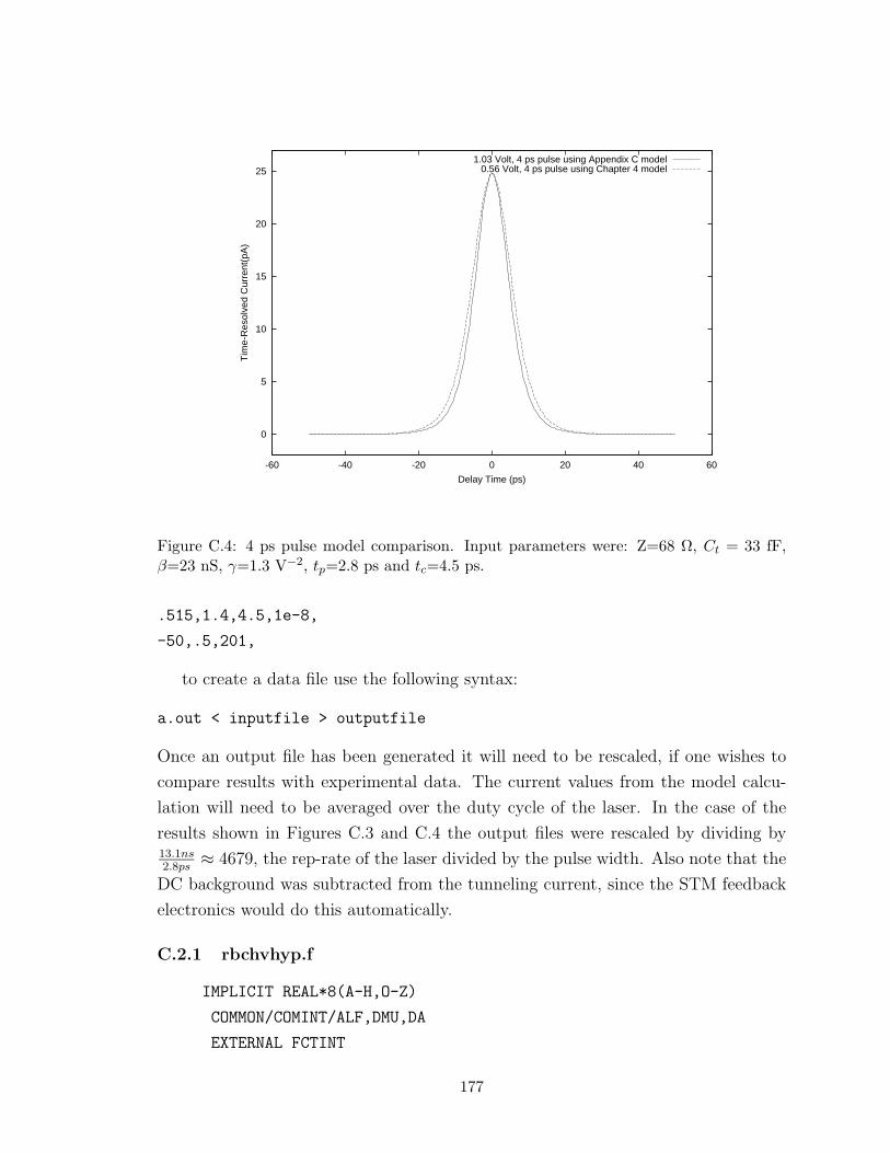
0
5
10
15
20
25
-60 -40 -20 0 20 40 60
Tim
e-R
esol
ved
Cur
rent
(pA
)
Delay Time (ps)
1.03 Volt, 4 ps pulse using Appendix C model0.56 Volt, 4 ps pulse using Chapter 4 model
Figure C.4: 4 ps pulse model comparison. Input parameters were: Z=68 Ω, Ct = 33 fF,β=23 nS, γ=1.3 V−2, tp=2.8 ps and tc=4.5 ps.
.515,1.4,4.5,1e-8,
-50,.5,201,
to create a data file use the following syntax:
a.out < inputfile > outputfile
Once an output file has been generated it will need to be rescaled, if one wishes to
compare results with experimental data. The current values from the model calcu-
lation will need to be averaged over the duty cycle of the laser. In the case of the
results shown in Figures C.3 and C.4 the output files were rescaled by dividing by13.1ns2.8ps
≈ 4679, the rep-rate of the laser divided by the pulse width. Also note that the
DC background was subtracted from the tunneling current, since the STM feedback
electronics would do this automatically.
C.2.1 rbchvhyp.f
IMPLICIT REAL*8(A-H,O-Z)
COMMON/COMINT/ALF,DMU,DA
EXTERNAL FCTINT
177

CALL UERSET(1,LEVOLD)
1 READ(5,*,END=90)Z,C,BETA,GAM
WRITE(6,200)Z,C,BETA,GAM
200 FORMAT(’#’,5G15.7)
READ(5,*,END=90)V0,W1,W2,RERR
WRITE(6,200)V0,W1,W2,RERR
ALF=W1/(C*Z)
DMU=W1/W2
CALL FVPEAK(DMU,TM,VM,IER)
VCON=V0/VM
C VLI=8.D0*VCON*W2
FACI=VCON**3*(ALF/(ALF-DMU))**2*W1*GAM
XLIM1=DLOG(0.1D0*RERR)
XLIM2=-XLIM1/DMIN1(DMU,1.D0)
5 READ(5,*,END=1)DST,DEL,ND
IF(ND.LT.1)GO TO 1
DO 20 ID=1,ND
D=(ID-1)*DEL+DST
DA=DABS(D)/W1
CH=DCADRE(FCTINT,XLIM1,XLIM2+DA,0.D0,RERR,ERR,IER)
C CH=(CH*FACI+VLI)*BETA
CH=CH*FACI*BETA
WRITE(6,215)D,CH,IER
215 FORMAT(1X,G15.7,G18.10,I5)
20 CONTINUE
GO TO 5
90 STOP
END
FUNCTION FCTINT(T)
IMPLICIT REAL*8(A-H,O-Z)
COMMON/COMINT/ALF,DMU,DA
VP=VPULSE(T,DMU)+VPULSE(T-DA,DMU)
F0=VPULSE(T,ALF)+VPULSE(T-DA,ALF)-VP
FCTINT=F0*F0*VP
RETURN
END
FUNCTION VPULSE(T,DMU)
178

IMPLICIT REAL*8(A-H,O-Z)
DATA PI/3.1415926535897932D0/
IF(T.LE.0.D0)THEN
CV=1.D0+DMU
FN=DEXP(T)
R=FN/(FN+1.D0)
FN=FN/((0.5D0*FN+0.5D0)**2*(DMU+1.D0))
SUMP=FN
ELSE
CV=1.D0-DMU
FN=DEXP(-T)
R=FN/(FN+1.D0)
FN=FN/((0.5D0*FN+0.5D0)**2*(DMU-1.D0))
SUMP=FN+4.D0*PI*DMU/DSIN(PI*DMU)*DEXP(-DMU*T)
ENDIF
DO 20 N=1,100
FN=(N+1)*R*FN/(CV+N)
SUM=SUMP+FN
IF(SUM.EQ.SUMP)GO TO 30
20 SUMP=SUM
WRITE(6,*)’ VPULSE DID NOT CONVERGE’
30 VPULSE=SUM
RETURN
END
SUBROUTINE FVPEAK(DMU,T,VM,IER)
IMPLICIT REAL*8(A-H,O-Z)
DATA PI/3.1415926535897932D0/
IF(DMU.LE.0.D0)THEN
WRITE(6,*)’ VOLTAGE NOT DEFINED’
RETURN
ENDIF
IF(DMU.GT.0.61096148D0)THEN
W=1.D0/DMU
F=W*W
T=(W*(781386480.D0+F*(11881642080.D0+17855925901.D0*F)))/
1 (781386480.D0+F*(12402566400.D0+24209906625.D0*F))
ELSE
179

IF(DMU.GT.0.1918343D0)THEN
T=DLOG(DMU)/(DMU-1.D0)
ELSE
T=DLOG(DMU+DMU*DMU)/(DMU-1.D0)
ENDIF
ENDIF
IF(DMU.LT.0.95D0)GO TO 25
CV=1.D0+DMU
DO 20 IT=1,25
IER=IT
R=1.D0/(DEXP(-T)+1.D0)
FN=DMU/(DMU+1.D0)
SUMP=FN
DO 10 N=1,200
FN=(N+1)*R*FN/(CV+N)
SUM=SUMP+FN
IF(SUM.EQ.SUMP)GO TO 15
10 SUMP=SUM
WRITE(6,*)’ SUM DID NOT CONVERGE’
15 FN=1.D0-SUM
W=DTANH(0.5D0*T)
FN=FN/(W+(0.5D0*DMU+0.25D0/W-.75D0*W)*FN)
T=T+FN
IF(T.LE.0.D0)T=DABS(T-FN)*0.5D0
IF(DABS(FN).LE.1.D-10*T)GO TO 50
20 CONTINUE
IER=-1
GO TO 45
25 CON=PI*DMU/DSIN(PI*DMU)*DMU
CV=1.D0-DMU
DO 40 IT=1,25
IER=IT
W=DEXP(-T)
R=W/(W+1.D0)
FN=-DMU*(1.D0+W)**(DMU+1.D0)
SUMP=CON*DEXP(CV*T)*(1.D0+W)**2+FN/CV
DO 30 N=1,200
180

FN=(N-1-DMU)*R*FN/N
SUM=SUMP+FN/(N+CV)
IF(SUM.EQ.SUMP)GO TO 35
30 SUMP=SUM
WRITE(6,*)’ SUM DID NOT CONVERGE’
35 FN=1.D0-SUM
W=DTANH(0.5D0*T)
FN=FN/(W+(0.5D0*DMU+0.25D0/W-.75D0*W)*FN)
T=T+FN
IF(T.LE.0.D0)T=DABS(T-FN)*0.5D0
IF(DABS(FN).LE.1.D-10*T)GO TO 50
40 CONTINUE
IER=-1
45 WRITE(6,*)’ FVPEAK DID NOT CONVERGE’
50 VM=1.D0/(DCOSH(0.5D0*T)**2*DMU)
RETURN
END
181