Journal of Micromechanics and Microengineering, 17(10): Issue
15
Instructions for use Title Microfabrication of an anodic oxide film by anodizing laser-textured aluminium Author(s) Jha, Himendra; Kikuchi, Tatsuya; Sakairi, Masatoshi; Takahashi, Hideaki Citation Journal of Micromechanics and Microengineering, 17(10): 1949-1955 Issue Date 2007-10 Doc URL http://hdl.handle.net/2115/30212 Rights Copyright © 2007 IOP Publishing Ltd. Type article (author version) File Information JMM17.pdf Hokkaido University Collection of Scholarly and Academic Papers : HUSCAP
Transcript of Journal of Micromechanics and Microengineering, 17(10): Issue

Instructions for use
Title Microfabrication of an anodic oxide film by anodizing laser-textured aluminium
Author(s) Jha, Himendra; Kikuchi, Tatsuya; Sakairi, Masatoshi; Takahashi, Hideaki
Citation Journal of Micromechanics and Microengineering, 17(10): 1949-1955
Issue Date 2007-10
Doc URL http://hdl.handle.net/2115/30212
Rights Copyright © 2007 IOP Publishing Ltd.
Type article (author version)
File Information JMM17.pdf
Hokkaido University Collection of Scholarly and Academic Papers : HUSCAP

Microfabrication of anodic oxide film by anodizing of
laser-texture aluminium
Himendra Jha*, Tatsuya Kikuchi, Masatoshi Sakairi,
and Hideaki Takahashi
Lab. of Interface Microstructure Analysis (LIMSA),
Division of Materials Science and Engineering,
Graduate School of Engineering, Hokkaido University,
Kita-13, Nishi-8, Kita-Ku, Sapporo 060-8628, Japan.
E-mail: [email protected] or
Abstract
A simple method for the fabrication of microstructures of aluminium anodic oxide film
(anodic alumina) by anodizing laser-textured aluminium is demonstrated. In the process, the
aluminium substrate was first textured by a low power laser beam, and then the textured
aluminium was subjected for anodizing, to develop a continuous, thick porous layer on the
textured surface. Microstructures with a few to several tens of micrometers depth were
fabricated successfully on the anodic oxide film using various combinations of laser power
density and laser scanning speed. Removing the film from the aluminium substrate enables
the fabrication of various 2D and 3D microstructures from anodic alumina.
1. Introduction
Fabrication of structures of ceramics and various types of glasses, polymers etc, in micro-
and nano-scale play an important role in many areas of modern technology. Such micro-
sized structures have been used to fabricate various types of micro-devices for optical,
chemical, biological, medical and other applications in the rapidly growing tiny-
technologies field [1-3].
1

The porous anodic oxide film formed on aluminium, prepared by anodizing
in oxalic acid solution, is similar to leuco-sapphire or glass ceramics, which are
widely used in microelectronics. Porous anodic oxide film has sufficient mechanical
strength and stability in extreme environments, which makes it suitable for the
subsequent fabrication of hybrid integrated circuits [4]. Taking advantage of the
properties of anodic oxide film formed by anodizing, various applications have been
reported in the past few decades [5-9]. Recently, thick porous anodic oxide film has
been recognized as a promising material for the fabrication of micro devices [10-12].
The anodic oxide film of aluminium is transparent and can resist very high
temperatures, therefore it may be a good candidate for the fabrication of micro
components for photonic as well as for high temperature processes. In these contexts,
fabrication of microstructures of anodic oxide film of aluminium, with a simple,
precise, and cost-effective method is of great interest in many areas of micro-
technology.
Photolithographic techniques are well suited for production large numbers of
identical parts, as they are very efficient for high throughput processes. However,
there are many types of geometries and miniaturized components that are not
compatible or cost-effective if processed with photolithographic tools. In those cases,
other techniques such as direct-write processes offer unique advantages and
capabilities for the fabrication of miniaturized components [13,14]. Among direct-
write processes, laser tools have been successfully used for the fabrication of
miniature components [15-18]. The growing number of companies developing laser
micromachining techniques for an expanding number of applications is proof that
laser micromachining is a well-established fabrication technique.
The present research aims to establish a technique for the fabrication of
microstructures of anodic alumina by anodizing of laser textured aluminium surfaces,
followed by substrate dissolution. The effects of parameters like laser power density
and laser scanning speed on the shape and size of the resulting microstructures are
investigated. Additionally, microstructures of the anodic oxide film of aluminium
are fabricated to demonstrate the capabilities of the technique.
2. Experimental Methods
2

2.1 Specimen and pre-treatment
Highly pure (99.99 wt.%) 350μm thick aluminium specimens were ultrasonically
cleaned in ethyl alcohol for 10 minutes. The specimens were immersed in CH3COOH 78
vol.% + HClO4 22vol.% solution at 283K, for 5 min with a constant voltage of 28V to get
the electropolished surface on aluminum [19]. The various steps preformed for the
fabrication of microstructures on anodic oxide film by anodizing laser-textured aluminium
is summarized in Fig. 1 (a).
Figure 1: (a) Different steps for the fabrication of microstructures by anodizing of laser textured aluminium surface. (b) Laser irradiation setup for the texturing of the aluminium.
2.2 Laser texturing
The electropolished aluminium specimens were textured by a second harmonic,
solid state, pulsed Nd:YAG laser (Spectra Physics; GCR-100 series) with 532 nm
wavelength, 8 ns pulse width, and 50 Hz frequency. The laser set-up is shown in Fig. 1(b).
The specimens were irradiated by laser inside a plastic cell filled with doubly distilled water,
which placed on a movable stage (KOHZU; PK 569-B). Power density of the laser beam
was measured by Ophir power measurement head (12A-P-SH), just before the laser
irradiation.
3
2.3 Anodizing and aluminum removal
The laser-textured specimens were anodized in 0.22 M H2C2O4 solution, at 293 K for 90
min (unless otherwise stated) with a constant current of 100 Am-2. In some experiments, the
specimens were subjected to pore-sealing in boiling doubly distilled water for 15 min. The
aluminium substrate was removed either by immersing in saturated SnCl4 solution or by
amalgamating aluminium in saturated HgCl2 solution at room temperature. As the solutions
does not affect the oxide film, a portion of aluminum should be exposed to solution (if
completely bounded by the oxide film or others). Care should be taken while working with
HgCl2 because of bad impacts on health as well as environment.
2.4 Analysis
The microstructures were analyzed by confocal scanning laser microscopy, CSLM
(Lasertec, 1LM21D), and field emission scanning electron microscopy, FE-SEM (JEOL,
JSM-6500F).
3 Results and Discussion
3.1 Laser texturing on aluminium surface
Microstructures of different dimensions and shapes were textured on aluminium by
scanning a focused laser beam across the surface. The shape and size of the micro-textured
structures can be controlled by varying the laser power density and laser scanning speed.
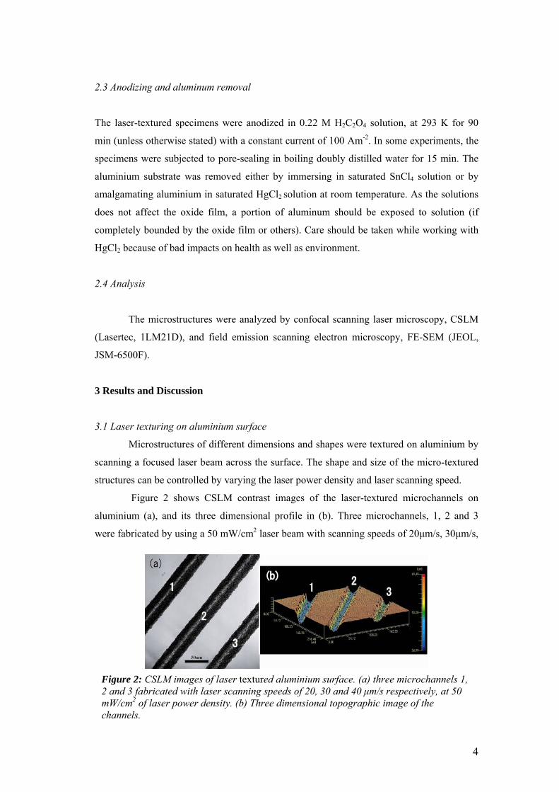
Figure 2 shows CSLM contrast images of the laser-textured microchannels on
aluminium (a), and its three dimensional profile in (b). Three microchannels, 1, 2 and 3
were fabricated by using a 50 mW/cm2 laser beam with scanning speeds of 20μm/s, 30μm/s,
Figure 2: CSLM images of laser textured aluminium surface. (a) three microchannels 1, 2 and 3 fabricated with laser scanning speeds of 20, 30 and 40 μm/s respectively, at 50 mW/cm2 of laser power density. (b) Three dimensional topographic image of the channels.
4
and 40μm/s respectively. It can be seen that, the microchannels have good edge definition
and consistent shape throughout their length. Figure 2(b) shows that, increasing the scanning
speed significantly decreases the depth and width of the texture, and there is a high degree
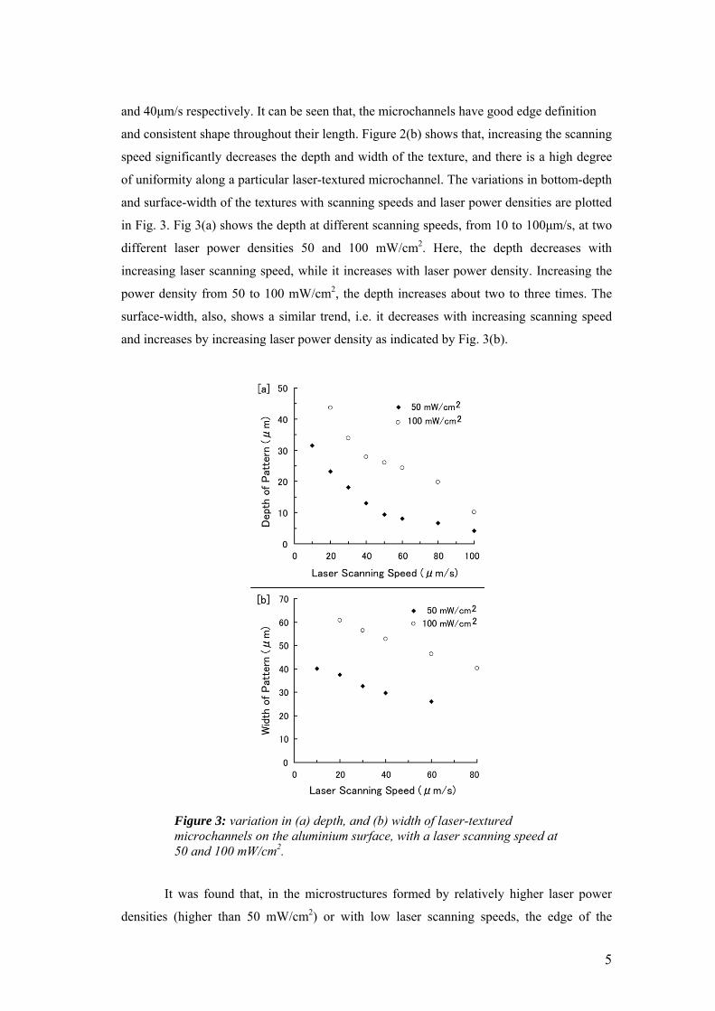
of uniformity along a particular laser-textured microchannel. The variations in bottom-depth
and surface-width of the textures with scanning speeds and laser power densities are plotted
in Fig. 3. Fig 3(a) shows the depth at different scanning speeds, from 10 to 100μm/s, at two
different laser power densities 50 and 100 mW/cm2. Here, the depth decreases with
increasing laser scanning speed, while it increases with laser power density. Increasing the
power density from 50 to 100 mW/cm2, the depth increases about two to three times. The
surface-width, also, shows a similar trend, i.e. it decreases with increasing scanning speed
and increases by increasing laser power density as indicated by Fig. 3(b).
Figure 3: variation in (a) depth, and (b) width of laser-textured microchannels on the aluminium surface, with a laser scanning speed at 50 and 100 mW/cm2.
It was found that, in the microstructures formed by relatively higher laser power
densities (higher than 50 mW/cm2) or with low laser scanning speeds, the edge of the
5
microch
laser beam across the aluminium surface forms a continuous groove
n the irradiated surface by ablation. Controlling the movement and direction of the laser
irradiati
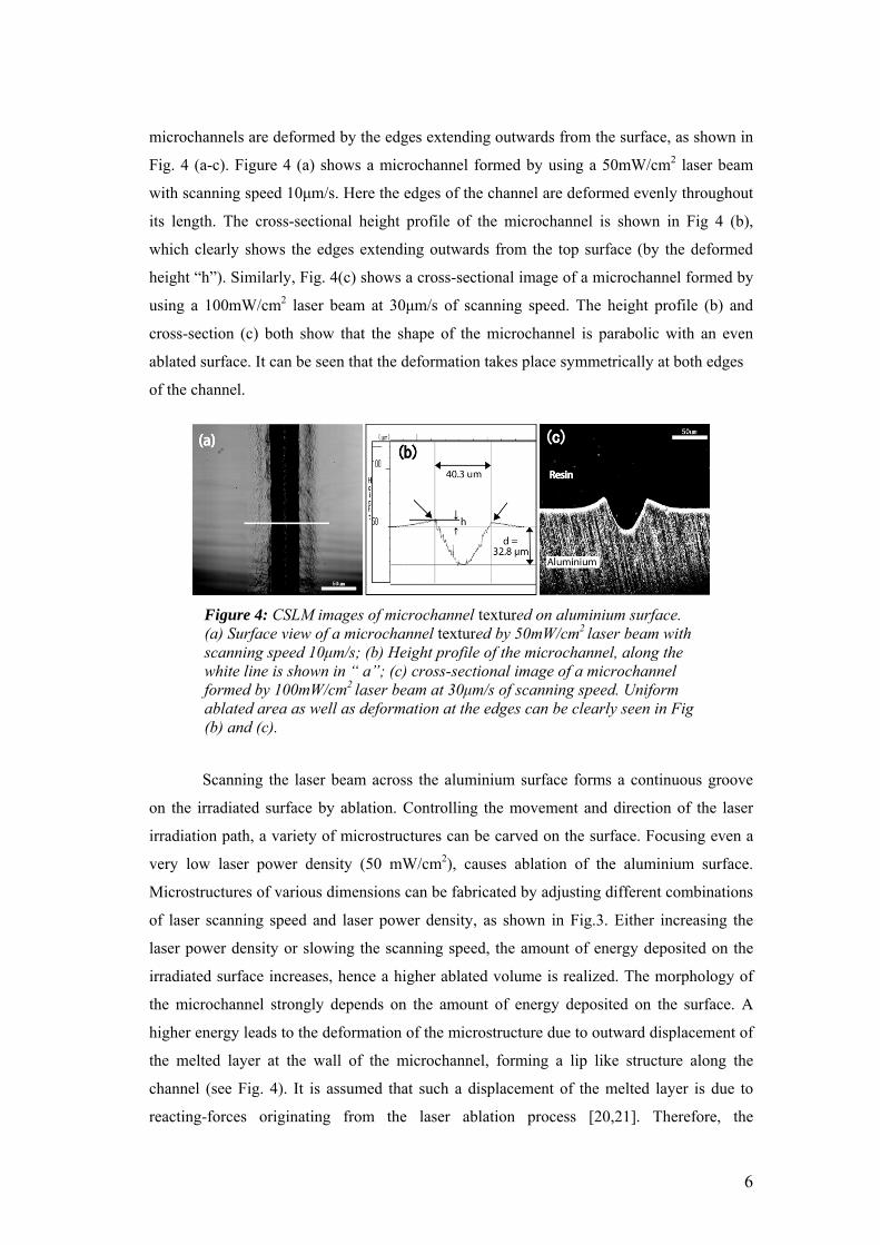
Figure 4: CSLM images of microchannel textured on aluminium surface. (a) Surface view of a microchannel textured by 50mW/cm2 laser beam with scanning speed 10μm/s; (b) Height profile of the microchannel, along the
annels are deformed by the edges extending outwards from the surface, as shown in
Fig. 4 (a-c). Figure 4 (a) shows a microchannel formed by using a 50mW/cm2 laser beam
with scanning speed 10μm/s. Here the edges of the channel are deformed evenly throughout
its length. The cross-sectional height profile of the microchannel is shown in Fig 4 (b),
which clearly shows the edges extending outwards from the top surface (by the deformed
height “h”). Similarly, Fig. 4(c) shows a cross-sectional image of a microchannel formed by
using a 100mW/cm2 laser beam at 30μm/s of scanning speed. The height profile (b) and
cross-section (c) both show that the shape of the microchannel is parabolic with an even
ablated surface. It can be seen that the deformation takes place symmetrically at both edges
of the channel.
Scanning the
white line is shown in “ a”; (c) cross-sectional image of a microchannel formed by 100mW/cm2 laser beam at 30μm/s of scanning speed. Uniform ablated area as well as deformation at the edges can be clearly seen in Fig(b) and (c).
o
on path, a variety of microstructures can be carved on the surface. Focusing even a
very low laser power density (50 mW/cm2), causes ablation of the aluminium surface.
Microstructures of various dimensions can be fabricated by adjusting different combinations
of laser scanning speed and laser power density, as shown in Fig.3. Either increasing the
laser power density or slowing the scanning speed, the amount of energy deposited on the
irradiated surface increases, hence a higher ablated volume is realized. The morphology of
the microchannel strongly depends on the amount of energy deposited on the surface. A
higher energy leads to the deformation of the microstructure due to outward displacement of
the melted layer at the wall of the microchannel, forming a lip like structure along the
channel (see Fig. 4). It is assumed that such a displacement of the melted layer is due to
reacting-forces originating from the laser ablation process [20,21]. Therefore, the
6
deformation is more pronounced with higher power densities and lower scanning speeds. It
was found that the microstructures formed by higher scanning speeds ( i.e., ≥40μm/s at
100mW/cm2, or ≥20μm/s at 50mW/cm2) either had very low or no such edge deformation.
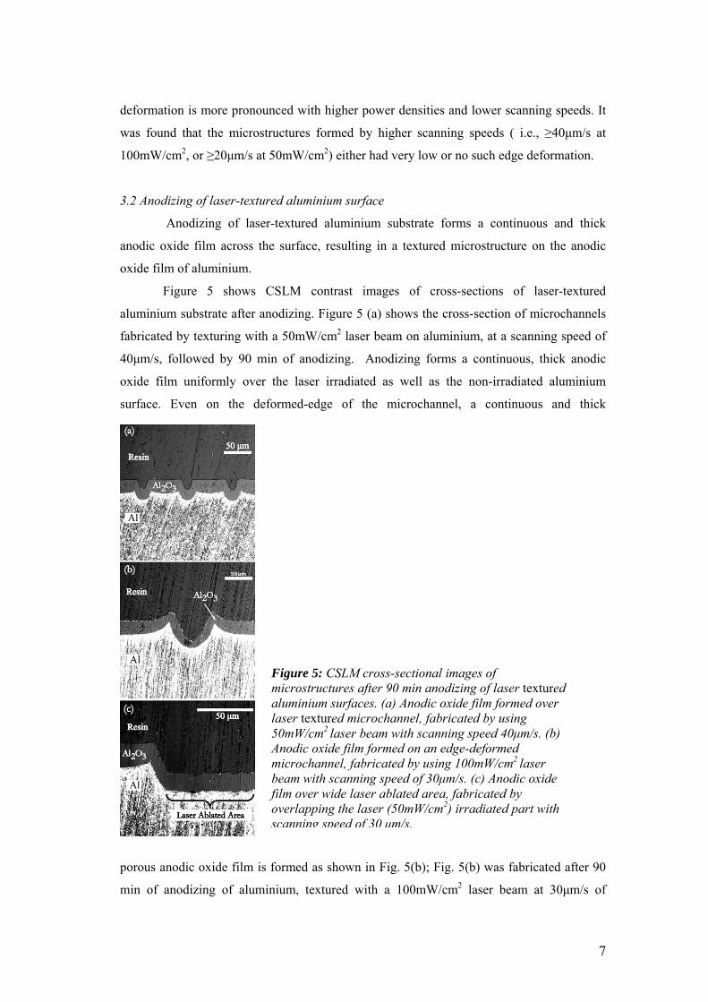
3.2 Anodizing of laser-textured aluminium surface
Anodizing of laser-textured aluminium substrate forms a continuous and thick
porous anodic oxide film is b); Fig. 5(b) was fabricated after 90
in of anodizing of aluminium, textured with a 100mW/cm2 laser beam at 30μm/s of
anodic oxide film across the surface, resulting in a textured microstructure on the anodic
oxide fi
nodizing. Figure 5 (a) shows the cross-section of microchannels
fabricat
lm of aluminium.
Figure 5 shows CSLM contrast images of cross-sections of laser-textured
aluminium substrate after a
ed by texturing with a 50mW/cm2 laser beam on aluminium, at a scanning speed of
40μm/s, followed by 90 min of anodizing. Anodizing forms a continuous, thick anodic
oxide film uniformly over the laser irradiated as well as the non-irradiated aluminium
surface. Even on the deformed-edge of the microchannel, a continuous and thick
m
Figure 5: CSLM cross-sectional images of microstructures after 90 min anodizing of laser textured aluminium surfaces. (a) Anodic oxide film formed over
sing
er
h
laser textured microchannel, fabricated by u50mW/cm2 laser beam with scanning speed 40μm/s. (b) Anodic oxide film formed on an edge-deformed microchannel, fabricated by using 100mW/cm2 lasbeam with scanning speed of 30μm/s. (c) Anodic oxide film over wide laser ablated area, fabricated by overlapping the laser (50mW/cm2) irradiated part witscanning speed of 30 μm/s.
formed as shown in Fig. 5(
7

scanning speed. Similarly, on a wider laser ablated area, the anodic oxide film forms
uniformly after anodizing as shown in Fig.5(c), which is a cross-section of a part of a
microchamber textured by partly overlapping microchannels. Figure 5 (c) shows that the
surface of the anodic oxide film formed over the laser textured surface is somewhat rougher
than that formed on the electropolished area. Figure 6 shows the change in depth (d) and
deformation height (h) of the microchannels, before and after anodizing for 90 min, with the
laser scanning speeds. The depth of the microchannels before and after anodizing does not
change significantly even after 90 min of anodizing as shown in Fig. 6 (a). In Fig. 6 (b), the
edge deformation height (h) is plotted against laser scanning speed before and after
anodizing for 90 min, at 50 and 100 mW/cm2 of laser power density. Here, generally the
deformation height (h) decreases almost linearly with increasing scanning speed, and
decreases slightly by the anodizing. The strong influence of the power density on the edge
deformation height can be understood from the results in Fig. 6(b).
Figure 7 shows the FE-SEM images of microstructures o
Figure 6: (a) Change in depth of laser-textured microchannels fabricated by 100 mW/cm2 laser beam, before and after anodizing for 90 min. (b) Variation in edge deformation height before and after anodization with scanning speeds at 50 and 100mW/cm2.
n anodic oxide film of
luminium, formed after anodizing of laser-textured aluminium surfaces. Here, the a
8
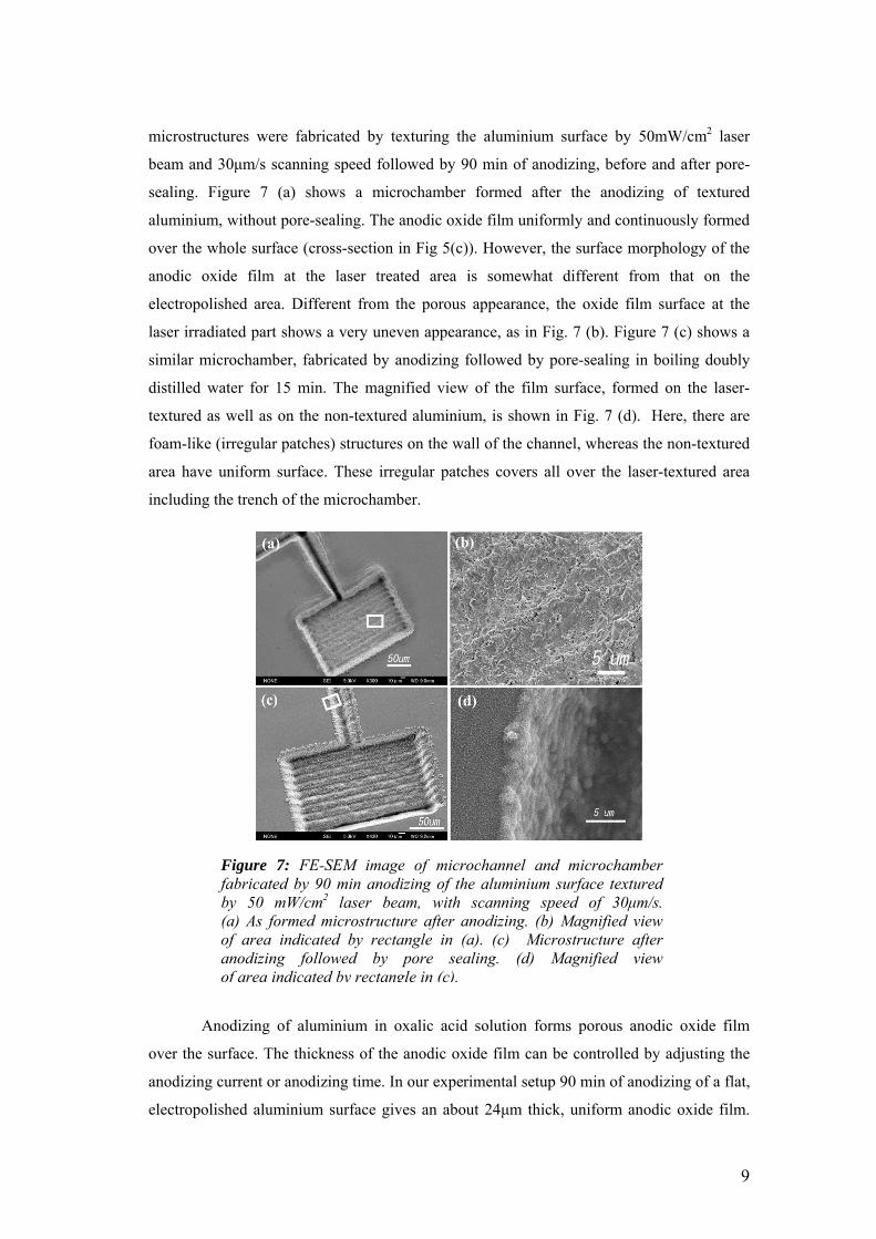
microst
acid solution forms porous anodic oxide film
over the surface. The thickness of the anodic oxide film can be controlled by adjusting the
anodizi
ructures were fabricated by texturing the aluminium surface by 50mW/cm2 laser
beam and 30μm/s scanning speed followed by 90 min of anodizing, before and after pore-
sealing. Figure 7 (a) shows a microchamber formed after the anodizing of textured
aluminium, without pore-sealing. The anodic oxide film uniformly and continuously formed
over the whole surface (cross-section in Fig 5(c)). However, the surface morphology of the
anodic oxide film at the laser treated area is somewhat different from that on the
electropolished area. Different from the porous appearance, the oxide film surface at the
laser irradiated part shows a very uneven appearance, as in Fig. 7 (b). Figure 7 (c) shows a
similar microchamber, fabricated by anodizing followed by pore-sealing in boiling doubly
distilled water for 15 min. The magnified view of the film surface, formed on the laser-
textured as well as on the non-textured aluminium, is shown in Fig. 7 (d). Here, there are
foam-like (irregular patches) structures on the wall of the channel, whereas the non-textured
area have uniform surface. These irregular patches covers all over the laser-textured area
including the trench of the microchamber.
Anodizing of aluminium in oxalic
Figure 7: FE-SEM image of microchannel and microchamber fabricated by 90 min anodizing of the aluminium surface textured by 50 mW/cm2 laser beam, with scanning speed of 30μm/s. (a) As formed microstructure after anodizing. (b) Magnified view of area indicated by rectangle in (a). (c) Microstructure after anodizing followed by pore sealing. (d) Magnified view of area indicated by rectangle in (c).
ng current or anodizing time. In our experimental setup 90 min of anodizing of a flat,
electropolished aluminium surface gives an about 24μm thick, uniform anodic oxide film.
9

Similarly, anodizing of the laser-textured aluminium, results in a continuous and uniform
anodic oxide film on the laser ablated as well as on the bare surface. The formation of such
an oxide film over the aluminium surface results in the texture observed on the film surface.
The shape and size of the microstructure on anodic oxide film is almost the same as that
fabricated on the aluminium surface. However, some deviation was observed in the case of
very low laser scanning speeds and with a higher power beam. In these cases, the oxide film
formed at the bottom of the microchannel was relatively thinner than on the surface. It is
evident that, during laser texturing the focused laser beam interact with the surface of the
aluminium, causing it to be heat-up, leading to the melting of the irradiated part. The melted
part may be displaced or ejected from the irradiated part and solidify when it cools; in the
same time debris formed all over the surface by solidifying the aluminium droplets and
fragments. Such type of melting and re-solidification of the surface makes it uneven with
different morphological structure than non-irradiated surface [22]. Anodizing of this uneven
aluminium surface gives rise to the anodic oxide film with rough and irregular outer surface.
Similarly, hydrothermal pore-sealing of porous anodic oxide film forms a highly crystalline
hydroxide layer on the external surface of the film [8]. Since the oxide film surface on the
laser-textured area is uneven, these parts develops irregular patches like hydroxide, as seen
in Fig. 7 (d); whereas the non-textured surface (where the oxide film surface is smooth)
have uniform hydroxide layer on the surface, as shown in the left part of the same figure.
Though the pore sealing of the film enhances the strength of the microstructures, high
surface roughness may limit its versatility in micro-fluidic applications.
Figure 8 shows FE-SEM images of microstructures on the anodic oxide film. The
structures were textured by a 50 mW/cm2 laser beam with 30μm/s scanning speed, followed
by anodizing for 90 min. Fig. 8 (a) shows a microstructure consisting of three
microchambers connected to each other by microchannels. The depth of the channels is
Figure 8: FE-SEM images of microstructures on anodic oxide film of aluminium fabricated by 90 min anodizing the aluminium surface textured by 50 mW/cm2 laser beam, with scanning speed 30μm/s. (a) Three microchambers (depth 35μm) connected
epth with microchannels (depth 27μm). (b) A long and continuous microchannel with d27μm. (c) Magnified view of a part of the microchannel in (b).
10

27μm, while the depth of the chambers is about 35μm. This is due to the partial overlap of
the laser-irradiated area in the case of microchamber. Figure 8(b) shows a long and
continuous microchannel of about 27μm depth. A magnified view of a portion of the
microchannel is shown in Fig. 8 (c), showing that the channel has good edge definition and
smooth inner surface. The depth at different parts of the microstructure can be changed by
varying the scanning speed during the laser texturing on the aluminium surface. Repeating
the laser scanning on already textured areas would further increase the depth at the site.
Various types of microstructures can be fabricated on the anodic oxide film by texturing the
aluminium substrate with laser beams followed by anodizing to the desired film thickness.
3.3 Microstructure of anodic alumina
Based on the textures on the aluminium surface, a wide variety of 2D and 3D
microstructures of anodic oxide film (anodic alumina) can be obtained by anodizing of the
textured-aluminium followed by removal of the remaining aluminium substrate.
Figure 9 (a) shows the FE-SEM image of closely-spaced parallel grooves on the
anodic oxide film. The structure was formed by anodizing of a laser textured surface for 150
min followed by hydrothermal pore-sealing and then dissolution of the aluminium substrate.
It can be seen that the microstructure is uniform without cracks or defects. The cross-section
in Fig. 9(b) shows that the microstructure has a uniform shape with good edge definition.
Similarly, micro-bumps on anodic oxide film were fabricated by anodizing of aluminium,
consisting of laser-textured craters, as shown in Fig 10 (a). The micro-scale craters were
first textured on electropolished aluminium surface, which on anodizing followed by
aluminium dissolution forms micro-bumps on the back (toward the substrate), as shown in
Figure 9: (a) Microstructure of anodic oxide film (anodic alumina) fabricated by anodizing and pore-sealing of laser textured aluminium surface followed by aluminium substrate dissolution. b) Magnified cross-sectional view of the microstructure in (a).
11

Fig. 10(b). The diameter of the micro-bumps is about 40μm at about 200μm intervals. The
magnified view of a micro-bump in Fig. 10 (c) shows a slightly irregular surface, due to the
anodizing of the uneven laser irradiated surface. The isolated anodic oxide film is fragile in
nature, and can easily break if not processed carefully. It was found that the thinner film
(about less than 10µm) was difficult to detach from the aluminium surface safely (unbroken),
due to the fragile nature as well as relatively stronger anchoring at laser textured area than in
smooth area.
The present method for the fabrication of microstructures of anodic oxide film of
aluminium provides a simple and cost-effective approach to the fabrication of a variety of
various 2D and 3D microstructures. The microstructures thus formed, after anodizing of the
laser textured surface (Fig. 8) will be suitable for the fabrication of various micro-fluidic
devices, here, the aluminium substrate attached to the anodic oxide film gives sufficient
mechanical support for the devices. Moreover, removing the anodized film from the
aluminium substrate provides a wide band-gap, transparent, and highly temperature resistant
microstructures of anodic alumina. These types of microstructures would be useful in the
design of various types of micro-components including photonic, high temperature
packaging, high temperature micro-devices etc.
Figure 10: Fabrication of micro-bumps on the anodic oxide film of aluminium. (a) Schematic of the different steps; (b) micro-bumps on the anodic oxide film of aluminium, and (c) magnified view of a micro-bump.
12

4. Conclusions
Microstructures can be textured on anodic oxide film of aluminium, by anodizing
the laser-textured aluminium substrate. The shape and size of the microstructures
significantly depends on the laser power density and laser scanning speeds. Increasing the
power density or decreasing the scanning speed, the size of the microstructures increase, and
deformation of the edges of the microstructures becomes significant in such cases.
Microstructures, displaying uniformity over extended-lengths and a well ordered shape can
be realized by this method. By removing the textured-anodized film from the aluminium
substrate, various 2D and 3D transparent microstructures of anodic oxide film of aluminium
can be fabricated with good precision.
Acknowledgement
The work is supported by a Grant-in-Aid (#19206078) from the Ministry of Education,
Culture, Sports, Science and Technology, Japan, and Light Metal Education Foundation of
Japan.
References
[1] Spearing S M 2000 Acta mater. 48 179-196
[2] Liwe L A, Zhang W, An L, Shah S, Luo R, Liu Y, Cross T, Dunn M L, Bright V,
Daily J W and Raj R 2001 American Ceramic Society Bulletin 80 25
[3] Han M, Hyun D-H, Park H-H, Lee S S, Kim C-H and Kim C G 2007 J. Micromech.
Microeng. 17 1184-91
[4] Mukhurov N I, Efremov G I and Kotova I F, 1997 Proc. of the Technical Digest of
IVMC’97 (Korea) 617-21
[5] Jha H, Kikuchi T, Sakairi M and Takahashi H 2007 Electrochem. Commun. 7 1597
[6] Masuda H, Ohya M, Asoh H, Nakao M, Nohtomi M and Tamamura T 1999 Jpn. J.
Appl. Phys. 38 L1403-05
[7] Martin C R 1994 Science 266 1961-66
[8] Jha H, Kikuchi T, Sakairi M and Takahashi H 2007 Electrochimica Acta 52 4724
[9] Kikuchi T, Akiyama Y, Ueda M, Sakairi M and Takahashi H 2007 Electrochimica
Acta 52 4480
[10] Delendik K I and Voitik O L 2001 Proc. SPIE, MICRO/MEMS 4592-49
[11] Jha H, Kikuchi T, Sakairi M and Takahashi H 2007 Appl. Phys. A 88 617-622
13

14
[12] Nadeem A, Mescher M, Rebello K, Weiss L W, Wu C, Feldman M and Reed M L
1998 Proc. of the 11th Annual Int. Workshop on Micro Electro Mechanical
Systems, MEMS 98 ( Germany) 274
[13] Pique A and Chrisey D B (eds) 2002 Direct-write technologies for rapid
prototyping applications (Academic Press)
[14] Oh K H, Lee M K and Jeong S H 2006 J. Micromech. Microeng. 16 1958-66
[15] Osgood R M, and Gilgen H H 1985 Annual Review of Materials Science 15 549-76
[16] Hnatovsky C, Taylor R S, Simova E, Rajeev P P, Rayner D M, Bhardwaj V R and
Corkum P B 2006 Appl. Phys. A 84, 47-61
[17] Arnold C B, Serra P and Pique A 2007 MRS Bulletin 32 23
[18] Stuke M, Mueller K, Mueller T, Williams K, Oliver R, Ohlberg D A A, Fuhr G and
Williams R S 2007 MRS Bulletin 32 32
[19] Wernick S, Pinner R and Sheasby P G 1987 The Surface Treatment and Finishing
of Aluminum and its Alloys (ASM International)
[20] Korner C, Mayerhofer R, Hartmann M and Bergmann H W 1996 Appl. Phys. A 63
123-31
[21] Fishburn J M, Withford M J, Coutts D W and Piper J A 2006 Appl. Surf. Sci. 252
5182-88.
[22] Dahotre Narendra B (ed.) 1998 Lasers in Surface Engineering (ASM International)