JOURNAL OF LA Removal Attacks on Logic Locking … · A major challenge for logic locking and...
14
JOURNAL OF L A T E X CLASS FILES, VOL. 14, NO. 8, AUGUST 2015 1 Removal Attacks on Logic Locking and Camouflaging Techniques Muhammad Yasin, Student Member IEEE , Bodhisatwa Mazumdar, Member IEEE , Ozgur Sinanoglu, Senior Member IEEE , and Jeyavijayan (JV) Rajendran, Member IEEE Abstract—With the adoption of a globalized and distributed IC design flow, IP piracy, reverse engineering, and counterfeiting threats are becoming more prevalent. Logic obfuscation techniques including logic locking and IC camouflaging have been developed to address these emergent challenges. A major challenge for logic locking and camouflaging techniques is to resist Boolean satisfiability (SAT) based attacks that can circumvent state-of-the-art solutions within minutes. Over the past year, multiple SAT attack resilient solutions such as Anti-SAT and AND-tree insertion (ATI) have been presented. In this paper, we perform a security analysis of these countermeasures and show that they leave structural traces behind in their attempts to thwart the SAT attack. We present three attacks, namely “signal probability skew” (SPS) attack, “AppSAT guided removal (AGR) attack, and “sensitization guided SAT” (SGS) attack”, that can break Anti-SAT and ATI, within minutes. Index Terms—Hardware security, Logic locking, Logic encryption, IC camouflaging, Boolean satisfiability, SAT. ✦ 1 I NTRODUCTION 1.1 The need for hardware IP protection In present-day semiconductor manufacturing, integrated cir- cuits (ICs) are designed and fabricated in a globalized multi- vendor environment, leading to concerns such as IC piracy, overproduction and counterfeiting [2]. A malicious foundry can reverse-engineer a GDSII layout file to obtain its gate-level netlist, or overbuild ICs to sell them illegally, leading to a serious economic loss to IC design companies [3], [4]. Moreover, the design may be pirated during test/assembly stages [5], or malicious circuits in the form of Hardware trojans may be embedded in the design [4]. Even an end-user may pirate the design using the state-of-the-art reverse engineering tools [6]. Reverse engineering can can extract design/technology details of an IC using imaging techniques. It involves several steps that include: depackaging an IC, delayering and imaging individual layers, and analyzing the collected images to identify design/IP details [6]. 1.2 Design-for-trust techniques Several design-for-trust countermeasures, including logic lock- ing [7], IC camouflaging [8], and split manufacturing [9] have been developed to prevent IP piracy and reverse engineering at- tacks [10], [11]. Among these countermeasures, logic locking [5], [7], [12]–[16] and IC camouflaging [8], [17], [18] have gained significant interest from the research community as they can be easily integrated within the existing IC design flow. Moreover, as opposed to split manufacturing, both of these countermeasures provide security against reverse engineering attacks carried out by a malicious end-user. Logic locking and IC camouflaging are typically referred to as hardware obfuscation techniques as they obfuscate/hide critical design details from the attacker. Logic locking. Logic locking is a gate-level technique; a design is locked by inserting additional locking circuitry post logic synthesis [11], [20], [21] as illustrated in Figure 1. The design A preliminary version of this paper was presented at IEEE Asia and South Pacific Design Automation Conference 2017 [1]. can be unlocked/made functional by only loading the secret key onto on-chip tamper-proof memory. An example locked netlist constructed using XOR/XNOR key gates is shown in Figure 2(c). IC camouflaging. IC camouflaging is a layout level technique; selected gates in the design are replaced with their camouflaged counterparts [8], [17]–[19], [22]. Camouflaged gates look identical from the top-view but can implement different functions. An example INV/BUF camouflaged gate is shown in Figure 3 [23]; the gate behaves either as a buffer or an inverter as dictated by the configuration of contacts 1 and 2 being either real or dummy. Transformations between logic locking and IC camouflaging have been proposed, enabling security analysis of both techniques using the same set of tools/algorithms [19]. Throughout this paper, we discuss the security aspects using the terminology associated with logic locking. Traditional locking locking. An important research question in logic locking (and IC camouflaging) is to find the gate locations in a netlist that can be locked (or camouflaged) with maximum security benefits per unit implementation overhead. The earlier re- search efforts focused on developing gate selection strategies (e.g., random [7], fault analysis-based [14], or interference-based [20]) that determine the gates to be locked (camouflaged) within the netlist [7], [8], [14], [20]. SAT attack resilient logic locking. Since the inception of a Boolean satisfiability (SAT) based attack against logic lock- ing/camouflaging techniques, the focus of research has shifted towards developing countermeasures that offer strong resilience against the SAT attack [17], [18], [24] (see Section 2.4 for details.). The attack uses specialized distinguishing input pat- terns (DIPs) for iteratively refining the key search space. The techniques developed recently to mitigate the SAT attack include SARLock [25], Anti-SAT [26], CamoPerturb [23], and AND-tree insertion (ATI) [27] (See Section 2.5 for details). The fundamental theme underlying these techniques is to utilize point functions implemented by AND/NAND/OR/NOR trees to minimize the number of keys eliminated per DIP.
Transcript of JOURNAL OF LA Removal Attacks on Logic Locking … · A major challenge for logic locking and...

JOURNAL OF LATEX CLASS FILES, VOL. 14, NO. 8, AUGUST 2015 1
Removal Attacks on Logic Locking andCamouflaging Techniques
Muhammad Yasin, Student Member IEEE , Bodhisatwa Mazumdar, Member IEEE , OzgurSinanoglu, Senior Member IEEE , and Jeyavijayan (JV) Rajendran, Member IEEE
Abstract—With the adoption of a globalized and distributed IC design flow, IP piracy, reverse engineering, and counterfeiting threatsare becoming more prevalent. Logic obfuscation techniques including logic locking and IC camouflaging have been developed toaddress these emergent challenges. A major challenge for logic locking and camouflaging techniques is to resist Boolean satisfiability(SAT) based attacks that can circumvent state-of-the-art solutions within minutes. Over the past year, multiple SAT attack resilientsolutions such as Anti-SAT and AND-tree insertion (ATI) have been presented. In this paper, we perform a security analysis of thesecountermeasures and show that they leave structural traces behind in their attempts to thwart the SAT attack. We present threeattacks, namely “signal probability skew” (SPS) attack, “AppSAT guided removal (AGR) attack, and “sensitization guided SAT” (SGS)attack”, that can break Anti-SAT and ATI, within minutes.
Index Terms—Hardware security, Logic locking, Logic encryption, IC camouflaging, Boolean satisfiability, SAT.
F
1 INTRODUCTION
1.1 The need for hardware IP protectionIn present-day semiconductor manufacturing, integrated cir-
cuits (ICs) are designed and fabricated in a globalized multi-vendor environment, leading to concerns such as IC piracy,overproduction and counterfeiting [2]. A malicious foundry canreverse-engineer a GDSII layout file to obtain its gate-level netlist,or overbuild ICs to sell them illegally, leading to a seriouseconomic loss to IC design companies [3], [4]. Moreover, thedesign may be pirated during test/assembly stages [5], or maliciouscircuits in the form of Hardware trojans may be embedded inthe design [4]. Even an end-user may pirate the design using thestate-of-the-art reverse engineering tools [6]. Reverse engineeringcan can extract design/technology details of an IC using imagingtechniques. It involves several steps that include: depackaging anIC, delayering and imaging individual layers, and analyzing thecollected images to identify design/IP details [6].
1.2 Design-for-trust techniquesSeveral design-for-trust countermeasures, including logic lock-
ing [7], IC camouflaging [8], and split manufacturing [9] havebeen developed to prevent IP piracy and reverse engineering at-tacks [10], [11]. Among these countermeasures, logic locking [5],[7], [12]–[16] and IC camouflaging [8], [17], [18] have gainedsignificant interest from the research community as they can beeasily integrated within the existing IC design flow. Moreover,as opposed to split manufacturing, both of these countermeasuresprovide security against reverse engineering attacks carried outby a malicious end-user. Logic locking and IC camouflaging aretypically referred to as hardware obfuscation techniques as theyobfuscate/hide critical design details from the attacker.
Logic locking. Logic locking is a gate-level technique; adesign is locked by inserting additional locking circuitry post logicsynthesis [11], [20], [21] as illustrated in Figure 1. The design
A preliminary version of this paper was presented at IEEE Asia and SouthPacific Design Automation Conference 2017 [1].
can be unlocked/made functional by only loading the secret keyonto on-chip tamper-proof memory. An example locked netlistconstructed using XOR/XNOR key gates is shown in Figure 2(c).
IC camouflaging. IC camouflaging is a layout level technique;selected gates in the design are replaced with their camouflagedcounterparts [8], [17]–[19], [22]. Camouflaged gates look identicalfrom the top-view but can implement different functions. Anexample INV/BUF camouflaged gate is shown in Figure 3 [23];the gate behaves either as a buffer or an inverter as dictated bythe configuration of contacts 1 and 2 being either real or dummy.Transformations between logic locking and IC camouflaging havebeen proposed, enabling security analysis of both techniques usingthe same set of tools/algorithms [19]. Throughout this paper, wediscuss the security aspects using the terminology associated withlogic locking.
Traditional locking locking. An important research questionin logic locking (and IC camouflaging) is to find the gate locationsin a netlist that can be locked (or camouflaged) with maximumsecurity benefits per unit implementation overhead. The earlier re-search efforts focused on developing gate selection strategies (e.g.,random [7], fault analysis-based [14], or interference-based [20])that determine the gates to be locked (camouflaged) within thenetlist [7], [8], [14], [20].
SAT attack resilient logic locking. Since the inception ofa Boolean satisfiability (SAT) based attack against logic lock-ing/camouflaging techniques, the focus of research has shiftedtowards developing countermeasures that offer strong resilienceagainst the SAT attack [17], [18], [24] (see Section 2.4 fordetails.). The attack uses specialized distinguishing input pat-terns (DIPs) for iteratively refining the key search space. Thetechniques developed recently to mitigate the SAT attack includeSARLock [25], Anti-SAT [26], CamoPerturb [23], and AND-treeinsertion (ATI) [27] (See Section 2.5 for details). The fundamentaltheme underlying these techniques is to utilize point functionsimplemented by AND/NAND/OR/NOR trees to minimize thenumber of keys eliminated per DIP.

JOURNAL OF LATEX CLASS FILES, VOL. 14, NO. 8, AUGUST 2015 2
Logic
synthesis
Physical
SynthesisFabrication Packaging
Functional IC
Third
party IP
System
specs.
Original
layoutOriginal
netlistWafer
Logic
locking
Locked
netlist
Camouflaging
Camouflaged
layout
Fig. 1. An illustration of logic locking and IC camouflaging in the context of IC design and fabrication flow.
G5
G3
G2
G1G4
a
b
c
O1
(a)
G3
G2
G1G4
a
b
c
O1G5
G6
(b)
G3
G2
G1G4
a
b
c
O1
K1
G5
K2
K1
K2
K3K3 G6
(c)
oi0
1i o
k
K1K1
oi
(d)
Fig. 2. (a) The original circuit. (b) A camouflaged circuit consisting of INV/BUF camouflaged gates. (c) Equivalent logic locked circuit constructedby replacing INV/BUF camouflaged gates with XOR key gates. (d) Transforming an INV/BUF camouflaged to its logic locking counterpart using aMUX; further simplification of the MUX-based gate to an XOR key gate [19].
Removal attack. In the SAT attack resilient techniques men-tioned above, the protection circuitry (implementation of a pointfunction) may be decoupled from the original circuit that needs tobe protected, rendering these techniques vulnerable to the removalattack. The removal attack aims at retrieving the original circuitby identifying and removing/bypassing the protection circuitry.The first step is to identify the protection circuitry, which may behampered due to layers of obfuscation in the design. This paper fo-cuses on evaluating the resilience of the SAT attack resilient logiclocking/camouflaging techniques against the removal attacks. Thecontributions of the paper are as follows:
1) We develop signal probability skew (SPS) attack that breaksAnti-SAT [26]. The SPS attack leverages the structural tracesin the netlist to identify and remove the Anti-SAT block withinminutes. The attack is scalable to large circuits; moreover, itbecomes more effective with increasing key size.
2) We identify the security vulnerabilities in the ATI tech-nique [27] and develop sensitization guided SAT (SGS) attackthat circumvents ATI in most of the circuits by exploiting thebias in the input distribution of the inserted AND-tree.
3) We demonstrate how SARLock [25] is vulnerable to simple re-moval attacks, whereas, CamoPerturb [23] exhibits resiliencyagainst the aforementioned attacks.
4) The simple yet effective attacks we propose emphasize theimportance of developing countermeasures without leavingstructural traces, which could be exploited in ways much
Fig. 3. Camouflaged layout of an INV/BUF gate. The gate behaves asan inverter or a buffer based on the configuration of circled contacts.When contact 1 is real and contact 2 is dummy, the gate behaves asan inverter. The gate behaves as a buffer when contact 1 is dummy andcontact 2 is real [23].
simpler than the main expected threat (i.e., the SAT attack).
2 BACKGROUND AND RELATED WORK
2.1 DefinitionsLogic locked netlist. The original netlist F is a Boolean
function F : I → O, where I = {0, 1}n and O = {0, 1}m.The locked netlist is a Boolean function L : I × K → O,where K = {0, 1}q . Upon activation using the secret key ks,L(i, ks) = F (i),∀i ∈ I . There are v key gates in L, eachimplementing p possible Boolean functions, determined by thekey k (consisting of dlog2pe-bits) .
Security of logic locking. A logic locking technique is con-sidered secure if the effort required by an attacker to determine thecorrect key value ks, or equivalently, retrieve the original circuitfunctionality is exponential in the number of key gates: O(2v).
Camouflaged netlist. The camouflaged netlistC : I×A→ Oconsists of u camouflaged gates, where the assignment A :[1, · · · , u] → G maps each camouflaged gate to an elementin G, the set of possible Boolean functions that a camouflagedgate can implement. For the correct assignment As, C(i, As) =F (i),∀i ∈ I .
Security of IC camouflaging. An IC camouflaging techniqueis considered secure if the effort required by an attacker to de-termine the correct assignment value As, or equivalently, retrievethe original circuit functionality is exponential in the number ofcamouflaged gates: O(2u).
Transformations. Transformations between logic locking andIC camouflaging enable security analysis of both techniques usingthe same set of algorithms [19]. The transformation T : C → Lreplaces each camouflaged gate with p gates (each implementingone of the functions in G) and a p : 1 MUX having dlog2pe selectinputs. The transformation for an INV/BUF camouflaged gate isillustrated in Figure 2(d). The logic locked netlist is Figure 2(c)is generated by replacing each INV/BUF in the camouflagednetlist in Figure 2(b) with its logic locking counterpart, i.e., anXOR/XNOR key gate [19].
Removal attack. A removal attack is a transformation R :L(I,K) → H(I) such that H(i) = F (i),∀i ∈ I . Thus, uponthe removal of the protection circuit, an attacker can obtain an

JOURNAL OF LATEX CLASS FILES, VOL. 14, NO. 8, AUGUST 2015 3
implementation that produces the correct output for every inputirrespective of the key value. For logic locking solutions thatcombine two or more logic locking techniques, it is essential thatan attacker is not able to target the techniques on an individualbasis.
2.2 Traditional obfuscation techniquesIn this subsection, we present a summary of traditional obfus-
cation techniques and attacks.Logic locking primitives. A wide variety of logic locking
primitives have been used. The combinational primitives includeXOR/XNOR gates [7], [14], [20], [21], AND/OR gates, multiplex-ers, whereas the sequential primitives include look-up tables [12]and obfuscated finite state machines (FSMs) [15], [30].
IC camouflaging primitives. Camouflaged gates can be con-structed by using real/dummy contacts [8], [31], manipulatingpolarities of dopants in the active regions of transistors [32]–[34],or adjusting the threshold voltage of transistors in a circuit [22].Available spaces in the design can also be filled using metallayers and filler cells to prevent insertion of malicious logic inthe design [35].
Traditional attacks. There exist multiple attacks, applicableto both logic locking and IC camouflaging, that can compromisetheir security. A summary of these attacks is presented in Table 1.In the sensitization attack, key bits are individually sensitized1 tothe outputs by applying judiciously crafted input patterns. Test-data mining [5] and hill climbing attack [21] leverage the vulnera-bilities associated with test data. Differential power analysis attackexploits the correlation between power consumption and key valueto extract the secret key [28]. The aforementioned attacks basicallyrely on divide-and-conquer approaches that are no more applicableto SAT attack resilient logic locking techniques, where standaloneimplementations of point functions (e.g. AND/NAND trees) areintegrated at with the original circuit.
2.3 Threat model(s)Logic locking and IC camouflaging have slightly different
threat models that differ basically in only one aspect. Logiclocking assumes an untrusted foundry, whereas IC camouflagingassumes a trusted foundry. However, both techniques assumethat the attacker has access to the same set of assets: a reverse-engineered netlist and a functional IC. The attacker uses computa-tional/simulation tools on the reverse-engineered (but obfuscated)netlist, while he/she exercises the functional IC (oracle) to producechip outputs for input patterns of interest.
The difference between logic locking and camouflaging at-tacks lies in when/how the attacker gets access to the requiredassets. Thus, both techniques can be evaluated for security on auniform basis. In this paper, we address security from a logiclocking perspective.
2.4 SAT attackThe SAT attack is applicable to both logic locking [24] and IC
camouflaging [17], [18]. As per the SAT attack threat model, theattacker has access to a reverse-engineered netlist and a functionalIC [17], [18], [24]. The main idea of the SAT attack is to reveal thecorrect key (or the correct functionality of camouflaged gates) byselectively applying the DIPs to a functional IC [24]. The attack
1. Sensitization of an internal line l to an output O refers to the condition(values applied from the primary inputs to justify the side input of gates on thepath from l to O to the non-controllable values of the gates) which surjectivelymaps l to O and thus renders any change on l observable on O.
rules out incorrect key values by using DIPs iteratively. A DIP isan input value for which at least two unique key values, k1 andk2, produce differing outputs, o1 and o2, respectively. Since o1and o2 are different, at least one of the key values is incorrect. Asingle DIP may rule out multiple incorrect key values, reducingthe computational effort of the attack.
Example. Let us consider an example SAT attack on thelogic locked circuit shown in Figure 2(c). Table 2 represents theoutput values of the locked circuit for different key and inputcombinations. The values (k0, . . . , k7) represent all possiblevalues for three key inputs {K1,K2,K3}. When the attack islaunched, it takes four DIPs to obtain the correct key. The lastcolumn in the table lists the keys eliminated in each iteration. Forexample, in iteration 4, the pattern 010 is used that eliminates allincorrect keys, and thus identifies k5 as the correct key.
The efficiency of the SAT attack depends on the order ofchoosing the DIPs. The total execution time of the SAT attackcomprising λ iterations with ti as the execution time for the i-th
iteration is T =λ∑i=1
ti [26]. The SAT attack can be mitigated if
either ti or λ increases exponentially with the key size.
2.5 SAT attack resilient obfuscationFigure 4 presents the recent SAT attack resilient logic lock-
ing/camouflaging techniques. The underlying idea of all thesetechniques is to utilize point functions to control the amount oferror injected into a circuit on the application of incorrect keyvalues. A point function is a Boolean function that produces theoutput value 1 at exactly one point. Example implementationsinclude AND gates and password checkers.
SARLock. As shown in Figure 4(a), SARLock integrates acomparator and a mask block with the original circuit to beprotected [25]. For the correct key value, no error is injected inthe circuit and the correct output is retained. For each incorrectkey value, an error is injected into the circuit for only oneinput pattern, leading to an incorrect output for the specificpattern. Assuming that F (I) is the original circuit, the outputO of the circuit locked using SARLock can be presented asO = F (I) ⊕ ((I == K) ⊕ (I == ks)), where K denotesthe key inputs, and ks is the correct key value.
Anti-SAT. The Anti-SAT block shown in Figure 4(b) com-prises two blocks, B1 = g(X,Kl1) and B2 = g(X,Kl2) [26].These blocks share the same inputs X , but are locked withdifferent keys Kl1 and Kl2. The outputs of B1 and B2 drive anAND gate to produce the output signal Y . The two blocks producecomplementary outputs when correct key value is applied; forall inputs, Y = 0, leading to a correct output. For an incorrectkey value, the output of B1 and B2 is 1 for a specific inputpattern; for that pattern, Y = 1, leading to an incorrect output.Assuming that Anti-SAT protects one of the primary outputs of theoriginal circuit F (I), the protected output O can be representedas O = F (I,Kl0) ⊕ (g(X ⊕Kl1) ∧ g(X ⊕Kl2)), where Kl0
represents the key for the logic locked circuit. We elaborate on thesecurity properties of Anti-SAT in Section 3.1.
CamoPertub. In CamoPerturb, the original logic cone F (I)is perturbed for exactly one minterm is to hide the true imple-mentation from an attacker [23]. The output of the logic cone forthe perturbed minterm is then restored using a camouflaged secretand a comparator block, as illustrated in Figure 4(c). Let F ′(I)represent the Boolean function for the perturbed logic cone, thenO = F ′(I)⊕ (I == cs), where cs is the camouflaged secret.

JOURNAL OF LATEX CLASS FILES, VOL. 14, NO. 8, AUGUST 2015 4
TABLE 1A comparison of the attacks against logic locking. The attacks are also applicable to the counterpart camouflaging techniques.
Attack Attackerlocation Attacker assets Attack method Proposed defense
Sensitization [8], [20] Foundry /end-user
1) Locked netlist2) Functional IC
Sensitization of key bits to circuit outputs Key-interference based logiclocking [13]
SAT [17], [24] Foundry /end-user
1) Locked netlist2) Functional IC
SAT-based algorithm that rules outincorrect keys iteratively
AES-based [13], Anti-SAT [26],SARLock [25], CamoPerturb[23], ATI [27]
Hill climbing [21] Foundry / testfacility
1) Locked netlist2) Test data
Start with a random key CK. Flip the bitsin CK based on the Hamming distance Test-aware logic locking [21]
Test-data mining [5] Foundry / testfacility
1) Locked netlist2) Test data
Find the key that maximizes faultcoverage and satisfies test data constraints Post-test activation [5]
Differential poweranalysis [28]
Foundry /end-user
1) Locked netlist2) Functional IC
Generate a differential trace from powersamples for each key value –
AppSAT [29] Foundry /end-user
1) Locked netlist2) Test data
Reduce a multi-layered defense tosingle-layered defense by augmentingSAT attack with random oracle queries
SARLock, Anti-SAT
Signal probabilityskew
Foundry /end-user 1) Locked netlist
Trace the Anti-SAT block using signalskew and remove it CamoPerturb
AppSAT guidedremoval
Foundry /end-user
1) Locked netlist2) Functional IC
Use AppSAT to find FLL key bits; tracekeys to identify and remove Anti-SAT CamoPerturb
Sensitization guidedSAT
Foundry /end-user
1) Locked netlist2) Functional IC
Guide the SAT attack using patterns fromsensitization attack CamoPerturb
Logic-Locked
CircuitI O
G(X,Kl1)
G(X,Kl2)
X
Kl2
Kl1
OFlip
(b)
Tamper-proof
Memory
Logic
cone
?= MaskFlip
I
K
(a)
Tamper-proof
Memory
Perturbed
logic cone
?=Restore
I
K
(c)
Camouflaged
secret
O
OI
(d)
Fig. 4. SAT attack resilient logic locking/camouflaging techniques. a) SARLock [25], b) Anti-SAT [26], c) CamoPerturb [23], and d) ATI [27].
TABLE 2Analysis of the SAT attack [24] against random logic locking [7]. Thered entries represent the keys identified as incorrect. k5 is the correct
key; the columns with all correct output values are shaded blue.
abc Y k0 k1 k2 k3 k4 k5 k6 k7 Incorrect keys identified000 0 1 1 1 1 1 0 1 1001 0 1 1 1 1 1 0 1 1010 0 1 1 1 1 1 0 1 1 iter 4: rest incorrect keys011 1 1 1 1 1 1 1 1 1100 0 1 1 1 1 1 0 1 0101 1 1 0 1 1 1 1 1 1 iter 3 : k1110 1 1 1 1 1 0 1 1 1 iter 1: k4111 1 1 1 0 1 1 1 1 1 iter 2: k2
AND/OR-tree insertion (ATI). While Anti-SAT [26], SAR-Lock [25], and CamoPerturb [23] add external point functionsto the original netlist, ATI aims at identifying these structuresinside the original netlist in an attempt to decrease the imple-mentation overhead [27]. The inputs of the identified AND/ORtree are camouflaged by inserting INV/BUF camouflaged gates asillustrated in Figure 4(d). The INV/BUF gates can be replacedwith the XOR/XNOR counterparts to obtain a logic locked AND-tree. Let us assume the original circuit can be represented as beingcomposed of two functions, F (I) = Tand(I) ◦ F ′(I), whereTand(I) is the AND-tree, F ′(I) is the rest of the circuit, and ◦ isthe Boolean operator integrating the two sub-circuits. The outputof the ATI circuit with the locked AND-tree can be represented asO = Tand(I,K) ◦ F ′(I). We discuss the security aspects of ATIin Section 4.1.
2.6 Signal probability skew
The signal probability skew attack, to be presented in Sec-tion 3.3, is based on the notion of probability skew. We define
signal probability skew sx of a signal x as,
sx = Pr[x = 1]− 0.5 (1)
where, Pr[x = 1] indicates the probability that signal x is 1. As0 ≤ Pr[x = 1] ≤ 1, the range of s is [−0.5, 0.5]. The SPS ofa signal denotes the amount by which a signal is distinguishablefrom a random guess, i.e., Pr[x = 1] = 0.5. An attacker has anegligible advantage of guessing the signal value over a randomguess if the corresponding SPS s is close to zero. For instance,all primary inputs and key inputs (unknown to the attacker) areequiprobable, hence their skew is zero.
Consider a two-input AND gate with inputs in1 and in2 withthe corresponding SPS values s1 and s2, respectively. The SPS ofthe output, sAND is defined as,
sAND = Pr[y = 1]− 0.5 = Pr[in1 = 1]Pr[in2 = 1]− 0.5
= 0.5(s1 + s2) + s1s2 − 0.25 (2)
If the inputs to an AND gate have zero SPS values, then sAND =−0.25, demonstrating the skew that every AND gate introduces.The SPS of an OR gate and an XOR gate is shown in Figure 5.It can also be noted that OR gates add a positive skew, whileXOR gates reduce the absolute skew, restoring it closer to zero.XOR/XNOR key gates, where the key inputs are treated as primaryinputs, introduce a skew of zero.
In MUX-based logic locking [14], the select input of a MUXis a key input with zero skew; the data inputs are intermediatesignals from the original circuit. The SPS of a MUX output canbe derived as,
sMUX = 0.5(s1 + s2) (3)

JOURNAL OF LATEX CLASS FILES, VOL. 14, NO. 8, AUGUST 2015 5
!"#
!$#!%&#'#()$*#+#()*,!"+!$-#.#!"!$##
!$#
!"#!/%&#'#.#$!"!$##
Fig. 5. SPS of OR and XOR gate outputs where s1 and s2 are the SPSof the inputs of the gates.
where s1 and s2 are the SPS of the inputs.
2.7 AppSAT attack
AppSAT, a recent variant of SAT attack, aims at reducing amulti-layered defense to single- layer (e.g. Anti-SAT+FLL to Anti-SAT) [29]. The AppSAT attack builds upon the SAT attack byquerying the functional IC with a fixed number of random DIPsat regular intervals and augmenting the CNF formula with newconstraints based on these DIPs. The attack terminates when theHamming distance between the correct output from the functionalIC and the locked netlist is very low (≈ 1
2n ), where n is the keysize. Upon termination, the attack returns an approximately correctkey that yields an approximate netlist [29].
While the AppSAT attack can produce only an approximatenetlist, it can be used as a pre-processing attack to peel off defensesone at a time. Subsequently, other attacks can be used to obtainthe exact netlist, as we will show in Section 3.6.
3 REMOVAL ATTACK ON ANTI-SAT
Fig. 6. An instance of the Anti-SAT block consisting of AND/NANDtrees [26].
3.1 Anti-SAT
As already mentioned in Section 2.5, the Anti-SAT blockconsists of two complementary blocks B1 = g(X,Kl1) andB2 = g(X,Kl2). The blocks integrated together render theSAT attack effort exponential in key size, i.e., in the numberof key bits. An instance of the Anti-SAT block is shown inFigure 6 [26]. At the inputs of B1 and B2, a set of XOR/XNORkey gates is inserted. The number of key inputs is the same asthe number of signals tapped from the logic locked circuit, i.e.,|Kl1| = |Kl2| = |X| = n. The resulting key size is thus 2n. Theoutput Y is implemented as Y = g(X ⊕ Kl1) ∧ g(X ⊕Kl2).The output Y is 0 for all inputs when the correct keys Kl1 andKl2 are applied. For incorrect keys, Y may take on the value 1,injecting error on an internal net in the netlist.
SAT attack resilience. The computational effort required bythe SAT attack decode the 2n key bits is defined in terms of thenumber of input vectors that make the function g equal to 1, i.e.,the on-set of g [26]. For an n-bit input vector L ∈ {0, 1}n, suchinput vectors are elements of the set,
LT = {L|g(L) = 1}, |LT | = p (4)
Anti-SAT constructs g in such a way that p is close to either 1 or2n − 1. For the Anti-SAT block in Figure 6, p = 1. The lower
bound on the number of SAT attack iterations (number of DIPs)to recover the 2n key bits of the Anti-SAT block is [26]:
λl =22n − 2n
p(2n − p). (5)
For p ∈ {1, 2n − 1}, the number of required iterations λl is 2n,i.e., exponential in the number of key bits in the Anti-SAT block.So, the SAT attack resilience of Anti-SAT hinges on p being eithervery small or very large. As Anti-SAT provides a provable measureto increase the SAT attack effort exponentially in key size, theconventional logic locking techniques need to be combined withthe Anti-SAT block to obtain foolproof logic locking.
Secure and Random Integration. The SAT attack resilienceof Anti-SAT also depends on the internal nets that drive the inputsof Anti-SAT block. Two integrations of Anti-SAT with originallogic locked circuit are considered in [26]: secure integration andrandom integration.
Secure Integration. In this scheme, the n inputs of the Anti-SAT block are driven by n primary inputs of the logic lockedcircuit. The output Y is connected to a wire in the original logiclocked circuit that is among the top 30% in observability.
Random Integration. In this scheme, the inputs as well as theoutput of the Anti-SAT block are connected to random wires inthe logic locked circuit. The SAT attack results show that secureintegration provides a higher resilience than random integration asit requires more iterations, resulting in a larger execution time toreveal the secret key [26].
3.2 Security vulnerabilities in Anti-SATThe main vulnerability of Anti-SAT is that it is incorporated
into the netlist at a single point, where its output Y is XORed withan internal net. Therefore, Anti-SAT defense has to rely on differ-ent obfuscation schemes that make the identification of the block(and, thus, signal Y) difficult for an attacker. At the same time,SAT attack resilience is ensured by choosing a skewed p value, asdictated by Equation 5, irrespective of the structural and functionalobfuscation. This basic construction principle inevitably leads tostructural traces that help identify the Anti-SAT block output ina given netlist; the proposed SPS attack exploits these traces tobreak Anti-SAT.
3.3 Signal probability skew attackIn this section, we present signal probability skew attack that
detects the output signal Y of the Anti-SAT block. We show thatthe absolute difference of the probability skew (ADS) of the inputsof a gate is the maximum for the gate G, which produces theoutput Y of the Anti-SAT block.
Threat model. The threat model of the SPS attack is weakerthan that of the SAT attack [24] and Anti-SAT [26]. SPS attackdoes not require access to a functional IC; the attack requires onlya reverse-engineered netlist. In contrast, the SAT attack requires afunctional IC as well.
Let us consider the skew of individual gates in the Anti-SATblock shown in Figure 6. The XOR key gates produce zero skewsignals. The blocks g(X,Kl1) and g(X,Kl2) comprise an n-input AND and an n-input NAND gate, respectively. The SPSsn−AND for the AND gate is defined as,
sn−AND =n∏i=1
(0.5 + si)− 0.5 (6)

JOURNAL OF LATEX CLASS FILES, VOL. 14, NO. 8, AUGUST 2015 6
where si is the SPS of the ith input. As si = 0, the SPS of n-inputAND gate in g(X,Kl1) is,
sg(X,Kl1) = 0.5n − 0.5 (7)
For large n, sg(X,Kl1) ≈ −0.5, indicating p ≈ 1. Similarly, forthe n-input NAND gate output in g(X,Kl2), the SPS is,
sn−NAND = 0.5−n∏i=1
(0.5 + si) (8)
As si = 0, the SPS of the NAND gate in g(X,Kl1) is,
sg(X,Kl1)= 0.5− 0.5n. (9)
For large n, sg(X,Kl1)≈ 0.5, indicating p ≈ 2n−1. The absolute
difference of the probability skew of the inputs of the AND gateG, ADSG, can be computed as,
ADSG = |sg(X,Kl1) − sg(X,Kl1)| = 1− 2× 0.5n (10)
If the number of inputs to the Anti-SAT block is high, ADSG =|sg(X,Kl1) − sg(X,Kl1)
| ∼= 1. ADSG close to 1 indicates thatthe two inputs of the gate G exhibit the highest skews but withopposite polarity. This property of gate G distinguishes it fromthe rest of the gates not only in the Anti-SAT block but also inthe entire circuit. The SPS attack on a logic locked circuit withthe Anti-SAT block comprises computing the SPS values of allthe gates in the circuit. The gate with the highest SPS value, i.e.,a gate with oppositely skewed inputs is the suspect gate G, theoutput gate of the Anti-SAT block. The SPS attack is described inAlgorithm 1.
SPS attack applies to arbitrary g and g. In case of n-inputOR gate and n-input NOR gate for the functions g and g, thecorresponding SPS values are,
sn−OR = 0.5−n∏i=1
(0.5− si), (11)
sn−NOR =n∏i=1
(0.5− si)− 0.5 (12)
The ADSG value will again be close to 1 for large n.SPS vs. SAT resilience. SPS attack is highly effective when
p ∈ {1, 2n − 1}; these values of p lead to the maximum ADSG.One option to reduce the effectiveness of the attack is to use avalue of p far from 1 and 2n− 1, reducing the signal skew values.However, any such attempt would make Anti-SAT vulnerable toSAT attacks as dictated by equation 5. Anti-SAT is thus corneredby SAT attack and the proposed SPS attack. This is furtherillustrated in Section 3.4.3.
Algorithm 1: Signal probability skew attack.Input : Cantisat // Locked netlist with Anti-SATOutput: Clock // Locked netlist after removing Anti-SAT
block1 ADSarr ← {}2 for gj ∈ Cantisat do3 ADSarr(gj)←compute ADS(Cantisat, gj)4 end5 G← find maximum (ADSarr) // Anti-SAT output6 Y ← find value from skew (G) // Correct value of Y7 Clock ← remove TFI(Cantisat, G, Y ) // Remove the gates
that are in TFI of gate G alone
10 20 30 40 50 60key size n
0.50
0.25
0.00
0.25
0.50
0.75
1.00
Ske
w
SPS(g)
SPS(g)
ADSG
Fig. 7. Impact of n on ADSG, the absolute difference of skew at theinputs of gate G, the output of Anti-SAT block, for p = 1. SPS(g) andSPS(g) represent the skew of the AND and NAND tree in the Anti-SATblock.
Removing the Anti-SAT block. In SPS attack, the gate G isidentified using the highest ADS trace. The logic locked circuitmay contain a few signals that exhibit high ADS values, close toADSG. These false candidates can be filtered out by checking forsimple structural traces. By analyzing the transitive fan-in (TFI) ofthe candidate gates and eliminating the gates whose TFI does notinclude at least 2n key inputs, we can correctly identify the gateG.
Identifying value of Y . Once G has been identified, thevalue of the output signal Y can be determined from sY . IfsY < 0, the value of Y in the functional IC is 0; otherwise,it is 1. Knowing the correct value of Y , one can trace backand discard the gates that are in the fan-in of signal Y alone.The remaining circuit re-synthesized the circuit using the correctvalue of Y . Upon removal, the Anti-SAT stripped circuit can berepresented as O = F (I,Kl0). To identify Kl0 for the logiclocked circuit (which is locked using traditional SAT attack-vulnerable techniques such as fault analysis-based logic locking),SAT attack can be launched.
Example. The objective of the SPS attack on the circuit inFigure 10 is to identify the output gate of the Anti-SAT block,i.e., G11. The highest five ADS values for the circuit are shownin Table 4. The pair of complementary signals, G8 and G10 withopposite SPS values leads to the highest ADS for G11, enablingthe precise detection of the output of the Anti-SAT block. The SPSfor the output of G11 is sY = −0.398, implying that the signalis skewed towards 0.
3.4 SPS attack results3.4.1 Experimental setup
The SPS attack experiments are conducted using ISCASbenchmark circuits [36] and OpenSPARC microprocessor con-trollers [37]. The SPS attack and the SAT attack are executed on aserver with 6-core Intel Xeon W3690 CPU, running at 3.47GHz,with 24 GB RAM [24]. The Anti-SAT block is integrated withfault analysis based logic locking [14], which is referred to asTOC’13(5%), following the convention used in [26].
3.4.2 Impact of key size (n)The number of keys in the basic Anti-SAT block is 2n, where
n is the number of keys in the individual blocks g and g. For theSPS attack to be effective, ADSG must increase with n. Figure 7
Fig. 8. Normalized attack resistance of the Anti-SAT block for n = 16. Forthe SAT attack, the resistance is the number of iterations of the attacknormalized by 65536. For the SPS attack, the resistance is specified as1−ADSG. The SPS attack is highly effective in region shaded red; theSAT attack is effective in the region shaded blue.
JOURNAL OF LATEX CLASS FILES, VOL. 14, NO. 8, AUGUST 2015 7
demonstrates that as n increases, ADSG increases exponentiallyinitially and then saturates close to a value of 1. The SPS attack issuccessful when ADSG is close to 1, representing a gate whoseinputs are skewed towards opposite values. As an example, forn = 16, the skew at the output of the block g (an AND tree)will be ≈ −0.5, whereas the the skew at the output of the blockg (a NAND tree) will be ≈ 0.5. The ADSG will be ≈ 1. Forlarger n values, ADSG approaches 1 even further. Thus, theattack effectiveness increases with n, which is counter-intuitivefor any attack.
3.4.3 SAT attack vs. SPS attackImpact of p on attack success. The Anti-SAT block offers the
highest resistance against the SAT attack when p ≈ 1 or p ≈ 2n;then, the number of iterations for the SAT attack is ≈ 2n. Theresistance is the least when p ≈ 2n−1. Figure 8 displays the SATattack resistance normalized by 2n = 65536 for n = 16.
The resistance to the SPS attack can be represented as 1 −ADSG. When ADSG ≈ 0, the resistance is the maximum; thisalso implies p≈ 2n−1 and the minimum resistance to the SATattack. The resistance to the SPS attack is the minimum whenp ≈ 1 or p ≈ 2n as demonstrated in Figure 8; for these valuesof p, the SAT attack resistance is the maximum. Thus, the twoattacks are complementary to each other. One of the attacks ishighly effective for any value of p. The regions of effectiveness ofthe SPS and the SAT attack are shown as red and blue regions,respectively, in Figure 8.
Attack execution time. Figure 9 shows that the execution timeof the SAT attack depends on the value of p, which dictates thenumber of iterations of the attack. For p = 1 and p = 65535,the attack takes more than a day to complete. For the SPS attack,which involves computing the signal probabilities of few gates (≈100 for n = 16), the attack time is a few seconds, and practicallynegligible compared to the execution time of the SAT attack.
3.4.4 SPS attack on multi-layered defenseIn practical settings, the Anti-SAT block is integragted with an
existing (SAT attack vulnerable) logic locking technique such asFLL [14]. For maximum SAT attack resistance, secure integrationis utilized. In secure integration of Anti-SAT (referred to asTOC’13(5%)+n-bit BA in [26]), n inputs of the Anti-SAT blockare connected to n primary inputs of the logic locked circuit [26].ADSG is represented as 1 − 0.5n−1, irrespective of the logiclocked circuit. For a successful attack, ADSG must be higherthan the ADS of all the other gates in the circuit.
Table 3 presents the results for the SPS attack on secure inte-gration. The column “HC ADS” displays the highest ADS valuefor the gates in the original circuit (excluding the gates in the Anti-SAT block). With n = 16, the gates with ADS ≥ (1 − 0.515)are candidates for the gate G. We observe that there is only onecandidate for gate G in all the circuits except for s15850. The
20
22
24
26
28
210
212
214
215
216−214
216−212
216−210
216−28
216−26
216−24
216−22
216−20
p
0.0
0.4
0.8
1.2
1.6
Execu
tion t
ime (
s)
1e5
24 hours
SAT attack
SPS attack
Fig. 9. Execution time of the SAT attack and the SPS attack on basicAnti-SAT block for n = 16. The execution time of the SAT attack is morethan a day for p ∈ {1, 2n − 1}, whereas, the execution time of the SPSattack is less than 2 minutes for all values of p.
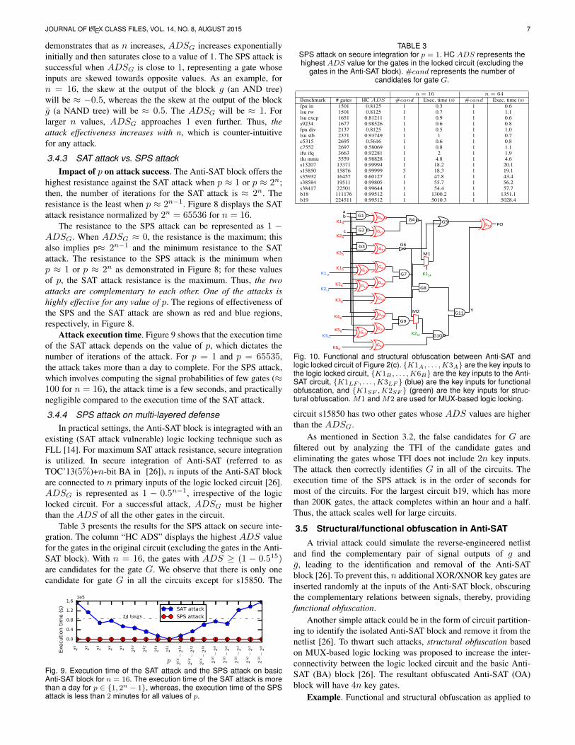
TABLE 3SPS attack on secure integration for p = 1. HC ADS represents thehighest ADS value for the gates in the locked circuit (excluding the
gates in the Anti-SAT block). #cand represents the number ofcandidates for gate G.
n = 16 n = 64Benchmark # gates HC ADS #cand Exec. time (s) #cand Exec. time (s)fpu in 1501 0.8125 1 0.3 1 0.6lsu rw 1501 0.8125 1 0.7 1 1.1lsu excp 1651 0.81211 1 0.9 1 0.6s9234 1677 0.98526 1 0.6 1 0.8fpu div 2137 0.8125 1 0.5 1 1.0lsu stb 2371 0.93749 1 1 1 0.7c5315 2695 0.5616 1 0.6 1 0.8c7552 2697 0.58069 1 0.8 1 1.1ifu ifq 3663 0.92281 1 2 1 1.9tlu mmu 5559 0.98828 1 4.8 1 4.6s13207 13371 0.99994 1 18.2 1 20.1s15850 15876 0.99999 3 18.3 1 19.1s35932 16457 0.60127 1 47.8 1 43.4s38584 19511 0.99805 1 55.7 1 56.2s38417 22501 0.99644 1 54.4 1 57.7b18 111176 0.99512 1 1300.2 1 1351.1b19 224511 0.99512 1 5010.3 1 5028.4
!"#
!$#
!%#
!&#!'#
(#
)#
*#
+,#
!-"#
-".#
-$.#
-%.#
!-$#
!-%#
!/#
!0"#
!.%#
!."#
!0$#
!.$#
!./#
!.&#
!0%#
!.'#
-"1#
-$1#
-%1#
-&1#
-'1#
-/1#
!-%#
-"02#
-$02#
-%02#
-"32#
-$32#
4"#
4$#
!5#
!6#
!7#
!"8#
!""#9#
Fig. 10. Functional and structural obfuscation between Anti-SAT andlogic locked circuit of Figure 2(c). {K1A, . . . ,K3A} are the key inputs tothe logic locked circuit, {K1B , . . . ,K6B} are the key inputs to the Anti-SAT circuit, {K1LF , . . . ,K3LF } (blue) are the key inputs for functionalobfuscation, and {K1SF ,K2SF } (green) are the key inputs for struc-tural obfuscation. M1 and M2 are used for MUX-based logic locking.
circuit s15850 has two other gates whose ADS values are higherthan the ADSG.
As mentioned in Section 3.2, the false candidates for G arefiltered out by analyzing the TFI of the candidate gates andeliminating the gates whose TFI does not include 2n key inputs.The attack then correctly identifies G in all of the circuits. Theexecution time of the SPS attack is in the order of seconds formost of the circuits. For the largest circuit b19, which has morethan 200K gates, the attack completes within an hour and a half.Thus, the attack scales well for large circuits.
3.5 Structural/functional obfuscation in Anti-SAT
A trivial attack could simulate the reverse-engineered netlistand find the complementary pair of signal outputs of g andg, leading to the identification and removal of the Anti-SATblock [26]. To prevent this, n additional XOR/XNOR key gates areinserted randomly at the inputs of the Anti-SAT block, obscuringthe complementary relations between signals, thereby, providingfunctional obfuscation.
Another simple attack could be in the form of circuit partition-ing to identify the isolated Anti-SAT block and remove it from thenetlist [26]. To thwart such attacks, structural obfuscation basedon MUX-based logic locking was proposed to increase the inter-connectivity between the logic locked circuit and the basic Anti-SAT (BA) block [26]. The resultant obfuscated Anti-SAT (OA)block will have 4n key gates.
Example. Functional and structural obfuscation as applied to

JOURNAL OF LATEX CLASS FILES, VOL. 14, NO. 8, AUGUST 2015 8
x1
xn
2
xn
2+1
xn
Y!"
(a)
x1
xn
Y
!"
(b)
Fig. 11. (a) Key gate inserted inside the tree of n-input AND gate; thechange in probability skew assists the SPS attack. (b) Key gate insertedat the output of n-input AND gate assists the SAT attack [24].
TABLE 4ADS values of the gates in the Anti-SAT block in Figure 10 in
descending order.
Gate G11 M1 M2 G8 G10ADS 0.6875 0.5 0.25 0.25 0.125
the logic locked circuit in Figure 2(c) is shown in Figure 10.The outputs of gates G8 and G10 form the output signals ofthe functions g and g, and hence are complementary signals; anattacker can attempt to find the potential complementary pair ofsignals, leading to the identification of the Anti-SAT block. TheAnti-SAT block, comprising an additional set of three key gates{GL1, GL2, GL3}, obfuscates the pair of complementary signaloutputs. Further, the MUXes M1 and M2 are used to increasethe inter-connectivity of the logic locked circuit and the Anti-SAT block. This structural obfuscation of Anti-SAT renders theidentification of the Anti-SAT block difficult for the attacker, asthe boundary between the two blocks is obscured.
SPS attack effectiveness on obfuscated Anti-SAT. The SPSattack is successful against obfuscated Anti-SAT (OA) as longas ADSG values do not deviate significantly as a conseqence ofobfuscation. Let us consider an n-input AND gate that constitutesthe function g in the Anti-SAT block. In Figure 11(a), the XORkey gate is inserted at a net inside the AND-tree, at the inputof final AND gate in this specific case. Let us assume s1 ands2 denote the skew at the inputs of the final AND gate. Priorto insertion of the key gate, s1 = s2 = 0.5
n2 − 0.5, and
sn−AND = 0.5n − 0.5 for the AND-tree. After the insertionof the key gate, s1 = 0, and hence the modified skew of then-input AND becomes s′n−AND = 0.5
n2 +1 − 0.5. When the
key gate is moved further to the output of AND gate as shownin Figure 11(b), sY = 0. The SPS attack, in its original form,would not be able to identify the gate G in such scenarios.Thus, by carefully inserting the key gates for functional/structuralobfuscation, a designer can defend against the SPS attack. Whileone can develop stronger variants of the SPS attack that rely onbetter heuristics to guide the attack in the presence of obfuscation,in this paper, we focus our efforts on developing a strong removalattack against OA that makes use of the recently developed attackknown as AppSAT [29].
3.6 AppSAT guided removal attack (AGR)
We propose AGR attack that integrates AppSAT with a simplestructural analysis of the locked netlist to develop a strong removalattack on OA. As opposed to the AppSAT attack, the AGR attackrecovers the exact netlist.
Threat model. The threat model for the AGR attack is same asthe threat model of the SAT attack [24] or ATI [27]. The attackerhas access to a locked netlist and a functional IC.
The attack begins by applying AppSAT to reduce FLL+OA toOA. As the AppSAT attack terminates, the key bits correspondingto FLL settle; i.e., their values don’t change over successive attack
Algorithm 2: AppSAT guided removal attack.Input : Cantisat // Locked netlist with Anti-SATInput : n // Key size for Anti-SATOutput: Clock // Locked netlist after removing Anti-SAT
1 #cand← num gates(Cantisat)2 while (#cand > 1 and !timeout) do3 launch appsat(4); // make 4 appsat calls4 candidates= {}5 for gj ∈ Cantisat do6 If Cgj ≈ 4n and R1(gj) ≈ R2(gj) ≈ 0.57 add gj to candidates8 end9 end
10 G← find maximum key count (candidates) // sortcandidates by Cg and pick the top-ranking one
11 Clock ← remove TFI(Cantisat, G) // Remove the gatesthat are exclusively in the TFI of the gate G
iterations. The key bit stability serves for distinguishing the Anti-SAT key bits from the FLL key bits.
Having peeled off the FLL layer, we next target the obfuscatedAnti-SAT through a simple structural analysis. The Anti-SATblock has 4n key inputs, all of which converge at the gate G,the output of Anti-SAT block. We determine the gate G by tracingthe transitive fan out of the Anti-SAT key inputs; it is the gatewhere all the 4n key bits converge.
In a real setting, AppSAT can only partially distinguish theFLL key bits from the Anti-SAT key bits. Similar to the FLLkey bits, certain Anti-SAT key bits (particularly those close tothe AntiSAT output) remain relatively stable over many iterations.Since the stable key bits could belong to either Anti-SAT or FLL,we use only the fluctuating key bits for structural analysis. Weexpect close to Cg = 4n fluctuating key bits to converge atthe gate G, while about 2n keys bits to converge at each ofits inputs, which are driven by the two trees that produce thecomplementary functions in the Anti-SAT block. At the inputsof gate G, the ratios R1 = Cin1
Cgand R2 = Cin2
Cgare close
to 0.5; here Cx represents the number of fluctuating keys thatconverge at a given gate. We identify the candidates for gate Gby checking for this property for each gate in the circuit. If theattack yields multiple candidate gates, we sort them based onthe number of key inputs that converge at a gate and pick thetop-ranking candidate as the gate G. Algorithm 2 describes theAGR attack. The attack further demonstrates that simple heuristicscould be used to build powerful attacks even on “provably-secure”hardware implementations.
3.7 AGR attack resultsIn this section, we present the results for the proposed AGR at-
tack against obfuscated Anti-SAT. Following the convention usedby [26], the attack results are presented for the secure integrationof OA with FLL, referred to as TOC’13(5%) + n-bit OA. Apartfrom the 2n key gates at the inputs for the Anti-SAT block,n additional XOR/XNOR key gates and n MUX key gates areinserted at the internal wires of the Anti-SAT block for functionaland structural obfuscation, respectively. In our implementation,each gate in Anti-SAT has two inputs.
Key bit stability. Figure 12 demonstrates the stability of thekey bits for the circuit c5315 when AppSAT attack is launched.The figure displays the percentage of consecutive previous itera-tions over which the value of a key bit has remained stable during

JOURNAL OF LATEX CLASS FILES, VOL. 14, NO. 8, AUGUST 2015 9
FLL(138)
Anti-SAT128x4=512
Fig. 12. Stability of key bits during AppSAT attack for the c5315TOC’13(5%)+128-bit circuit. The FLL key bits mostly remain stable andare easily distinguishable from the Anti-SAT key bits.
the attack; as soon as a key bit value flips, the count for the bitis reset to zero. It can be observed that most of the Anti-SAT keybits keep fluctuating and are easily distinguishable.
Attack success. Table 5 presents the results of the AGR attack.#cand denotes the number of valid candidates for gate G. Wereport #cand upon timeout of one hour to provide insights intothe attack behaviour. In most of the circuits, there is only onecandidate for G, demonstrating the effectiveness of the AGRattack. In a few cases, the attack may return more than onecandidate for G, since certain FLL bits may not have settled yet.We observe that these candidates are often the Anti-SAT gateslocated close to the gate G. Upon sorting the candidate gatesbased on the number of key inputs that converge at the gate (Cg),we identify gate G at the top of the ranked list of candidates. GateG was therefore identified successfully in 100% of the cases.
Execution time. The attack execution time is dominated bythe time for AppSAT. In our experiments, we set the AGR attacktimeout to one hour. This is sufficient for the attack to terminatesuccessfully since we are not interested in the values of the keybits. We rather need to classify key bits as stable or fluctuatingbased on their activity over successive attack iterations.
For the smaller circuits such as s5378, the attack terminatessuccessfully within a few seconds with a single candidate. Evenfor the circuit b19 with more than 200K gates, the attack reducesthe valid candidates to 938 within one hour. These 938 candidatesare then sorted to identify gate G successfully.
TABLE 5AGR attack on TOC’13(5%) + n-bit OA for n = 128 and p = 1. #canddenotes the number of valid candidates for the gate G upon a timeoutof one hour. Upon sorting the list of candidates based on Cg , the gate
G always has the first rank, implying 100% success rate.
Benchmark #cand Rank of G Exec. time (s)s5378 1 1 8.5ifu dcl 1 1 8.9fpu in 1 1 10.7lsu rw 1 1 10.7lsu excp 1 1 8.9s9234 1 1 9.4fpu div 1 1 9.4lsu stb 1 1 10.2c5315 1 1 11.7c7552 1 1 10.5ifu ifq 1 1 1.0tlu mmu 14 1 3600.0s13207 10 1 3600.0s15850 28 1 3600.0s35932 1 1 57.6s38584 22 1 3600.0b18 710 1 3600.0b19 938 1 3600.0
(a) (b)
Fig. 13. Examples of AND/OR-tree insertion: a) A camouflaged AND-tree with camouflaged INV/BUF gates inserted at its inputs [27], b) Thelocked counterpart of the AND-tree with XOR/XNOR key gates insertedat its inputs, using the transformations in [19]. Both trees achieve thesame level of security against the SAT attack [17], [24].
TABLE 6SAT attack resilience of ATI [27] for a 3-input AND gate with XOR keygates inserted at the inputs. For any DIP, the SAT attack can eliminate
at most one key value: the one that injects an error at the output. 3denotes correct output; 7 denotes incorrect output.
Key/DIP 0 1 2 3 4 5 6 7k0 3 3 3 3 3 3 3 3k1 3 3 3 3 3 3 7 7k2 3 3 3 3 3 7 3 7k3 3 3 3 3 7 3 3 7k4 3 3 3 7 3 3 3 7k5 3 3 7 3 3 3 3 7k6 3 7 3 3 3 3 3 7k7 7 3 3 3 3 3 3 7
4 REMOVAL ATTACK ON ATI4.1 AND tree insertion
As opposed to Anti-SAT [26], SARLock [25], and CamoPer-turb [23] that integrate external point functions with the originalnetlist, ATI identifies and reuses such structures inside the originalnetlist in order to decrease the implementation overhead [27].Once an AND/OR tree is identified in the netlist, the inputs of thetree are camouflaged by inserting INV/BUF camouflaged gates.Alternatively, using the transformations described in Section 1.2,the same tree may be locked by inserting XOR/XNOR key-gatesat the inputs, delivering the same level of security against the SATattack [19]. To be consistent with the previous discussion on SATattack, we will discuss the security of ATI from a logic lockingperspective. Figure 13 shows a camouflaged AND tree and itslogic locked counterpart.
4.1.1 ATI resilience to SAT attackSimilar to other SAT attack resilient logic locking techniques,
ATI attempts to render the number of DIPs exponential in thenumber of key gates by controlling the distinguishing ability ofindividual DIPs [27]. This is illustrated in Table 6 for a 3-inputAND-tree. It can be noted that exactly one incorrect key valuecan be eliminated by any of the input patterns, except for onespecial input pattern which, if applied, can identify all incorrectkeys. There exists no known algorithm that can identify the specialDIP from the analysis of the logic locked neltist. The numberof patterns that an attacker is expected to try (in a random trialapproach) prior to exercising the special input pattern is 2n−1.
4.2 Security challenges for ATIThere are multiple aspects that need to be considered prior to
identification/insertion of logic locked AND/OR trees in order toachieve strong resilience against SAT attack.

JOURNAL OF LATEX CLASS FILES, VOL. 14, NO. 8, AUGUST 2015 10
Node1
PO1
(a)
Node1
PO1PO2
(b)
Fig. 14. a) A non-decomposable AND tree, and b) a decomposableAND-tree [27]. Attacks on the decomposable tree can leverage divide-and-conquer strategies.
Node2Node1
stuck-at-0
Real AND tree Dummy AND tree
Fig. 15. Insertion of dummy AND-tree in the circuit. A stuck-at-0 fault isintroduced at the dummy input of the OR gate [27].
Existence of large non-decomposable trees. The securityof ATI is dictated by the size of the largest non-decomposableAND/OR-tree in the circuit, i.e., a tree where all internal nodeshave a fanout of 1. If the internal nodes of an AND/OR-tree havemultiple fanouts, an attacker can partition the tree into subtreesand attack the sub-trees on an individual basis. An example non-decomposable AND tree and a decomposable tree are presented inFigure 14(a) and (b), respectively. For sufficient security againstthe SAT attack, large non-decomposable AND/OR trees, e.g., with64 or 128 inputs, are required. Such large trees are rare in commonbenchmark circuits as will be illustrated in the experimental results(Section 4.4).
Bias in the input distribution. Contrary to the externallyintegrated AND/OR trees in Anti-SAT, the inputs of an internalAND/OR-tree may not be the primary inputs. Consequently, theinput distribution of the tree will be biased; not all input valueswill be equiprobable at the tree inputs. An attacker may exploitthis bias to reduce the attack effort.
Dummy AND/OR trees. To ensure the formation of a largeenough non-decomposable AND/OR tree, Li et al. [27] propose toinsert dummy AND/OR trees in the circuit and integrate themwith an original tree identified in the circuit, as illustrated inFigure 15. The dummy AND-tree Tdummy(I,K1), with keyinput K1, is integrated with the original AND-tree in the circuitusing a camouflaged OR gate. A permanent stuck-at-0 fault isintroduced at the input of the OR gate by manipulating thedopant polarities [27]. With the addition of the dummy AND-tree, the output of the ATI-locked circuit can be represented asO = F ′(I) ◦ Tand(I,K) ◦ Tdummy(I,K1). However, since theinserted tree is fake and disconnected functionally from the circuit,it is prone to removal attacks. We elaborate on this in Section 4.3.
Flexibility. Another major drawback of ATI is that it can onlyprotect the parts of a circuit where the desired AND/OR trees are
Fig. 16. Proposed SGS attack on ATI-locked netlist. The sensitizationattack computes a reduced set of attack patterns. The SAT attack usesthe computed patterns in conjunction with the functional IC output todetermine the correct key value.
present inherently. It does not offer a designer the flexibility tochoose the logic to be protected.
4.3 Sensitization-guided SAT attackIn this section, we present the sensitization-guided SAT attack
that exploits the security vulnerabilities of ATI to discover thecorrect key values using a small number of DIPs (� 2n). Theattack consists of two main stages, sensitization and the SAT attackas illustrated in Figure 16. The sensitization stage computes attackpatterns that are used to guide the SAT attack described in [24].
Threat model. The threat model for the SGS attack is same asthe threat model of the SAT attack [24] or ATI [27]. The attackerhas access to a locked netlist and a functional IC.
4.3.1 Stage 1. SensitizationThe objective of the sensitization stage is to compute attack
patterns that are used as DIPs by the SAT attack. This stageexploits two observations about the inserted AND(/OR) tree, asillustrated in Figure 17:
1. Bias in the input distribution. The bias in the inputdistribution of an n-input AND-tree implies that the tree inputstake on only a subset of 2n possible values. This reduction is dueto the logic in the transitive fanin (TFI) of the AND-tree, i.e., thelogic between the primary inputs of the circuit and the AND-treeinputs. This bias in input distribution allows an attacker to applyonly a subset of DIPs, i.e., those that bring unique values to theAND-tree inputs.
2. Sensitization of the injected error. The AND/OR-treeintroduces an error in the tree output for certain incorrect keyvalues. However, even if an error is injected at tree output, it maynot be sensitized to a primary output of the netlist; the effect of theerror may be masked by the logic in the transitive fanout (TFO)of the AND-tree. In VLSI testing, detection of a stuck-at-0 (1)fault requires that the fault be a) activated by assigning a value 1(0) to the fault location, and b) propagated to a primary output.
K0 K1 K2 K3 K4
I0
I1
I2
I3
I4
O0
O1
O2
O3
O4
TFI TFOAND-
tree
All DIPs DIPs at AND-tree inputs DIPs sensitizing faults to POs
Pri
ma
ry i
np
uts
Pri
ma
ry o
utp
uts
Key inputs
Fig. 17. An illustration of how the sensitization stage reduces the numberof the required DIPs. The gates in the TFI of the tree introduce bias andreduce the number of patterns received at the tree inputs. The gates inthe TFO hamper the sensitization of errors activated at the output of theAND tree and further narrow down the attack pattern space.

JOURNAL OF LATEX CLASS FILES, VOL. 14, NO. 8, AUGUST 2015 11
G2
G1ab
c
G3
G4
g1
g3
g2 K1
K2
K3
O1G5
Fig. 18. An example of pruned input pattern space as identified by thesensitization stage. The locked AND tree G4 has three inputs: g1, g2,and g3. The TFI logic prevents the tree inputs from taking on the values001,010, and 101. The TFO logic further reduces the number of feasibleinputs; overall, only two out of eight possible input combinations, 011and 000, are feasible for the AND tree inputs.
Thus, the manifestation of the effect of an incorrect key at theprimary outputs is analogous to the detection of a stuck-at faultat the output of the AND-tree. If the ATI defense was constrainedto identify AND trees that directly feed a PO, the error would beguaranteed to be sensitized; however, there would be further needfor dummy AND-trees as well.
Feasible input patterns. Overall, only a subset of total 2n (nis number of inputs of the AND tree) DIPs are deemed feasible,i.e., they can manifest the error in the circuit output. The SATattack uses the error at the output as a hint for identifying incorrectkey values [17], [24]. The smaller the number of input patternsused by the attack, the lower the computational effort of the attack.The effectiveness of the sensitization stage is determined by thereduction in the number of attack patterns.
Example. For the netlist in Figure 18, the locked AND-treehas three inputs: g1, g2 and g3. Due to the impact of the TFIlogic, the input values, 001, 010 and 101 cannot be assigned tothe tree inputs. The TFO logic further narrows down the feasibleinput space; only two input patterns 011 and 000 are feasible forthe tree inputs. Thus, the SAT attack can be launched using onlytwo input patterns. While the reduction ratio is relatively small forthis illustrative example, a significant reduction is achievable forlarger circuits as will be demonstrated in Section 4.4.
4.3.2 Stage 2. SAT attackThe attack patterns computed by the sensitization stage are
used to guide the SAT attack and extract the correct key byeliminating all the incorrect keys. The set of computed patternsis sufficient for a successful SAT attack since the set containsall the patterns that introduce observable error(s) in the circuit.The SAT attack does not need to compute any further DIPs andcompletes within a single iteration. The SAT solvers can inherentlyleverage the input bias and, apparently, render the sensitizationstage redundant. However, as explained in the next subsection,the sensitization stage helps identify real/dummy AND trees andprevents the SAT attack from running into long trails.
4.3.3 Identifying dummy AND/OR treesTo tackle the challenge of dummy AND/OR trees, we follow
a simple divide-and-conquer strategy. We assume that1) The attacker knows the location of the key gates (or alterna-
tively, the camouflaged gates).2) The dummy AND tree inputs are the primary inputs of the
circuit (or wires close to the primary inputs) so that the issuesrelated to the input bias are resolved [27].
3) The dummy AND-tree is large (e.g. 64 or 128) inputs.4) None of the gates inside the dummy tree fan out to the gates
in the original circuit. Only the output of AND (OR) treeis connected to a dummy OR (AND) gate; one input of the
connecting OR (AND) gate is stuck-at-0 (1) [27] as illustratedin Figure 15.
Based on these realistic assumptions, which are in line with thethreat model in [27], we identify a candidate dummy AND/ORtree in the netlist based on the input bias, and remove it from thenetlist. To quantify the input bias precisely, we use the notion offeasible input patterns. In the sensitization stage, we compute thenumber of feasible input patterns DIPSGS for each tree usingsharpSAT solver. The tree with the higher DIPSGS is assumed tobe dummy. Compared to KL divergence, which is an approximatemetric [27], DIPSGS is a precise metric, derived from VLSI testprinciples, that can be efficiently computed using the sharpSATsolver. We could launch the SAT attack directly on a tree withoutpre-computation of DIPSGS ; but then the SAT attack wouldpossibly run into long trails. Pre-computation of feasible inputpatterns prevents such situations. Upon removal of the dummyAND-tree, the ATI netlist reduces to F ′(I) ◦ Tand(I,K), whereTand denotes the real AND-tree. Mounting removal attack on thereal AND-tree Tand is not meaningful as it leads to extraction ofF ′(I), as opposed to F (I). We, therefore, proceed with the SGSattack on the tree that is assumed to be real. A successful SGSattack and the retrieval of the correct key validates the decisionabout the dummy AND-tree.
To verify the correctness of the key, we conduct the followingsimple test. From the correct key value returned by the attack, wecan determine the input pattern for which the AND(OR)-tree willoutput a 1(0). We need to verify the circuit operation for only oneinput pattern; the tree output is a 0(1) for the rest of the inputpatterns. Otherwise, we repeat the experiment by switching thedummy/real trees.
4.4 SGS attack resultsIn this section, we present the results for the SGS attack
on ISCAS, benchmark circuits [36], MCNC circuits [38], andOpenSPARC microprocessor controllers [37]. The experimentalsetup is the same as that for the Anti-SAT attack (presented in Sec-tion 3.4.1). The sensitization stage is launched using Minisat [39]solver. A miter circuit is constructed to find a pattern that candetect a stuck-at fault at the output of the AND/OR tree [40]. TheCNF formula for the miter is fed to the SAT solver to compute theattack patterns.
Size of typical AND/OR trees (ST ). To evaluate the effective-ness of ATI, we first report the size of the largest AND/OR treesin the benchmarks circuits under study. The AND/OR trees areidentified using the algorithm in [27]. We report only 22 circuitswith the largest AND/OR trees. Table 7 shows that the size ofthe trees identified in the benchmark circuits is rather small. Only11 out of the 22 reported circuits have a tree with 20 or moreinputs. Thus, to attain sufficiently large trees, e.g., with 64 or 128inputs, it becomes mandatory to add a dummy AND tree. In allexperiments, we assume a target tree size of 64. To identify andremove the dummy AND tree, we follow the procedure describedin section 4.3.3.
Percentage reduction in DIPs. Table 7 also shows DIPSGS ,which denotes the number of DIPs computed by the SGS attack;these patterns are sufficient to retrieve the correct key for the targetcircuit. It can be observed that the number of attack patterns �2ST , where ST represents the size of the identified AND/OR tree.The percentage reduction R in DIPSGS compared to DIPEXP ,computed as R = DIPEXP−DIPSGS
DIPEXP× 100%, is close to 100%
for about 50% of the circuits. Only a fraction of the DIPEXP

JOURNAL OF LATEX CLASS FILES, VOL. 14, NO. 8, AUGUST 2015 12
TABLE 7SGS attack results. ST denotes the number of inputs of the largestAND/OR tree in the circuit. DIPSGS denotes the number of attack
patterns returned by the SGS attack. DIPEXP is the expected numberof DIPs required by the SAT attack [17], [18], [27]. R is the percentagereduction in the number of DIPs. Texec denotes the execution time in
seconds.
Benchmark ST DIPEXP DIPSGS R(%) Texec(s)k2 104 1.01E+31 273 100.0 6.1s38417 35 1.72E+10 NA NA NAs15850 28 1.34E+08 NA NA NAdes 27 6.71E+07 28 100.0 1.3s38584 27 6.71E+07 1024 100.0 12.4b18 26 3.35E+07 NA NA NAb19 26 3.35E+07 NA NA NAtlu mmu 25 1.68E+07 NA NA NAlsu stb 24 8.39E+06 NA NA NAs13207 21 1.05E+06 6 100.0 1.3ifu ifq 20 5.24E+05 39680 92.4 6269.0c2670 18 1.31E+05 NA NA NAlsu excp 18 1.31E+05 2624 98.0 29.3c3540 17 65536 4096 93.8 100.1c1908 14 8192 2 100.0 1.3c880 14 8192 3072 62.5 32.0c5315 13 4096 991 75.8 10.3c432 12 2048 257 87.5 3.3fpu in 10 512 59 88.5 2.5ifu dcl 10 512 510 0.4 4.6lsu rw 10 512 59 88.5 2.8i8 9 256 70 72.7 9.9
patterns are sufficient to break circuits, such as k2 and des, with thelargest size of identified AND trees. For the same circuits, the SATattack alone requires DIPEXP = 2ST−1 patterns. For example,for the circuit k2 with ST = 104, DIPSGS = 273, compared toDIPEXP = 2103. The actual number of attack patterns used bythe SAT attack is almost the same as DIPSGS .
However, there are certain circuits, such as c2670, for whichthe SGS attack cannot complete within the allocated time of 10hours (and are marked as NA). For these circuits, the bias in theinput distribution of the tree is very small as most of the treeinputs are either the primary inputs of the circuit or the wiresclose to the primary inputs. As we discussed in Section 4.3.1, thesensitization stage leverages the bias in the input distribution toattain a reduction in the number of the required DIPs. When thereis zero or a very small bias in the input distribution, the attackeffectiveness reduces. Alternatively, ATI can be utilized only forthose circuits where large AND/OR trees exist close to the primaryinputs. Our empirical evaluation shows large trees (with larger than64 inputs) are rather rare; so, the designer has to resort to insertionof dummy AND trees, which can be easily removed using theproposed attacks.
Execution time. The execution time of the SGS attack de-pends on the circuit size and the number of the iterations of theattack. Each iteration computes a single attack pattern. Thus, forthe circuit ifu ifq with 39680 attack patterns, the execution timeis the highest. For most of the circuits, the execution time of theattack is in the order of a few seconds. Even for the circuit k2 witha 104-input AND tree, the attack completes in 6 seconds as thenumber of computed attack patterns is only 273. The timeout wasset to 10 hours.
5 REMOVAL ATTACKS ON SARLOCK ANDCAMOPERTURB
5.1 Security analysis of SARLock
In SARLock circuit, shown in Figure 4(a), the original logiccone is implemented intact without any modifications, whichmakes it vulnerable to removal attacks. As already mentioned in
Section 2.5, in SARLock,O = F (I)⊕((I == K)∧(I == ks)).An attacker has to isolate the protection circuitry comprising ofan XOR, comparator and mask block; he/she can then removethe protection circuitry and extract/pirate the original IP. Thecomparator is functionally composed of XNOR gates and anAND tree, which can be easily identified using existing AND-treeidentification algorithms [27] or the k-cut detection used in [26].
SARLock is vulnerable to the proposed SPS attack. Thecomparator logic comprises internally of an AND-tree, which canbe identified using the skew values computed by the SPS attack.Upon the removal of the protection logic, the original functionO = F (I) is retrieved.
SARLock, however, is not vulnerable to the SGS attack.The effectiveness of the SGS attack depends on the bias in theinput distribution. In SARLock, the comparator inputs are tied toprimary inputs that do not exhibit any bias. The attack fails toachieve any reduction in the number of attack patterns.
5.2 Security analysis of CamoPerturb
As shown in Figure 4(c), the restore circuitry in CamoPer-turb [23] consists only of a comparator and an XOR gate. InCamoPerturb, O = F ′(I)⊕ (I == cs). Although the SPS attackcan identify the comparator logic comprising the AND-tree, theremoval of the protection logic leads to the retrieval of the per-turbed/modified netlist F ′(I), as opposed to the targeted originalnetlist F (I). The comparator inputs are connected to the primaryinputs of the circuit; thus, there is no bias in the input distribution,and the SGS attack is ineffective against CamoPerturb.
5.3 Discussion
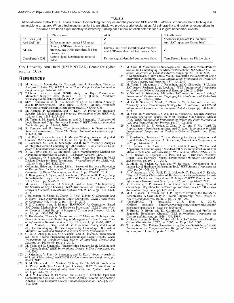
Table 8 summarizes the vulnerability of the existing SATattack resilient locking techniques to the proposed attacks. Theproposed SPS and SGS attacks are effective for specific coun-termeasures, Anti-SAT and ATI, respectively. However, as theempirical results demonstrate, the execution time of both attacks israther small. The attacks together serve as an evaluation platformthat can assist designers in quickly determining the possiblevulnerabilities of their logic locking/camouflaging solutions.
According to our analysis, CamoPerturb exhibits the best se-curity properties among all SAT attack resilient countermeasures.However, CamoPerturb protects the circuit for only one minterm.Thus, CamoPertub has to be combined with traditional logiclocking/camouflaging techniques.
6 CONCLUSION
Several countermeasures such as Anti-SAT and ATI have beendeveloped to thwart the SAT attack, and prevent IP piracy throughreverse engineering. Our security analysis identifies security vul-nerabilities in the existing countermeasures. We present threesimple attacks, SPS, AGR, and SGS, that can break Anti-SATand ATI, within minutes. The proposed attacks serve as a quickevaluation platform for future logic locking and camouflagingsolutions. We also provide insights for developing SAT attackresilient solutions that can withstand the proposed attacks.
7 ACKNOWLEDGEMENT
This work was supported in part by the Army Research Office(ARO) under Grant number 65513-CS; the National Science Foun-dation, Division Of Computer and Network Systems (NSF/CNS),under Grant number 1652842; and the New York University/New
JOURNAL OF LATEX CLASS FILES, VOL. 14, NO. 8, AUGUST 2015 13
TABLE 8Attack/defense matrix for SAT attack resilient logic locking techniques and the proposed SPS and SGS attacks. 3 denotes that a technique is
vulnerable to an attack. When a technique is resilient to an attack, we provide a brief explanation. All vulnerability and resiliency expectations inthis table have been experimentally validated by running each attack on each defense for our largest benchmark circuits.
SPS+Removal AGR SGS+RemovalSARLock [25] 3 3 SARLock inputs are PIs (no bias)Anti-SAT [26] Obfuscation may impact SPS values 3 Anti-SAT inputs are PIs (no bias)
ATI [27]Dummy AND-tree identified andremoved, real AND-tree identified butremoval failed
Dummy AND-tree identified and removed,real AND-tree identified but removal failed 3
CamoPerturb [23] Restore signal identified but removalfailed Restore signal identified but removal failed CamoPerturb inputs are PIs (no bias)
York University Abu Dhabi (NYU/ NYUAD) Center for CyberSecurity (CCS).
REFERENCES
[1] M. Yasin, B. Mazumdar, O. Sinanoglu, and J. Rajendran, “SecurityAnalysis of Anti-SAT,” IEEE Asia and South Pacific Design AutomationConference, pp. 342–347, 2016.
[2] “Defense Science Board (DSB) study on High PerformanceMicrochip Supply,” 2005, [March 16, 2015]. [Online]. Available:www.acq.osd.mil/dsb/reports/ADA435563.pdf
[3] SEMI, “Innovation is at Risk Losses of up to $4 Billion Annuallydue to IP Infringement,” 2008, [June 10, 2015]. [Online]. Available:www.semi.org/en/Issues/IntellectualProperty/ssLINK/P043785
[4] M. Rostami, F. Koushanfar, and R. Karri, “A Primer on HardwareSecurity: Models, Methods, and Metrics,” Proceedings of the IEEE, vol.102, no. 8, pp. 1283–1295, 2014.
[5] M. Yasin, S. M. Saeed, J. Rajendran, and O. Sinanoglu, “Activation ofLogic Encrypted Chips: Pre-test or Post-test?” IEEE Design, AutomationTest in Europe, pp. 139–144, 2016.
[6] R. Torrance and D. James, “The State-of-the-art in SemiconductorReverse Engineering,” IEEE/ACM Design Automation Conference, pp.333–338, 2011.
[7] J. A. Roy, F. Koushanfar, and I. L. Markov, “Ending Piracy of IntegratedCircuits,” IEEE Computer, vol. 43, no. 10, pp. 30–38, 2010.
[8] J. Rajendran, M. Sam, O. Sinanoglu, and R. Karri, “Security Analysisof Integrated Circuit Camouflaging,” ACM/SIGSAC Conference on Com-puter & Communications Security, pp. 709–720, 2013.
[9] R. W. Jarvis and M. G. McIntyre, “Split Manufacturing Method forAdvanced Semiconductor Circuits,” US Patent 7,195,931, 2007.
[10] J. Rajendran, O. Sinanoglu, and R. Karri, “Regaining Trust in VLSIDesign: Design-for-Trust Techniques,” Proceedings of the IEEE, vol.102, no. 8, pp. 1266–1282, 2014.
[11] Colombier, Brice and Bossuet, Lilian, “Survey of Hardware Protectionof Design Data for Integrated Circuits and Intellectual Properties,” IETComputers & Digital Techniques, vol. 8, no. 6, pp. 274–287, 2014.
[12] A. Baumgarten, A. Tyagi, and J. Zambreno, “Preventing IC Piracy UsingReconfigurable Logic Barriers,” IEEE Design & Test of Computers,vol. 27, no. 1, pp. 66–75, 2010.
[13] M. Yasin, J. Rajendran, O. Sinanoglu, and R. Karri, “On Improvingthe Security of Logic Locking,” IEEE Transactions on Computer-AidedDesign of Integrated Circuits and Systems, vol. 35, no. 9, pp. 1411–1424,2016.
[14] J. Rajendran, H. Zhang, C. Zhang, G. Rose, Y. Pino, O. Sinanoglu, andR. Karri, “Fault Analysis-Based Logic Encryption,” IEEE Transactionson Computers, vol. 64, no. 2, pp. 410–424, 2015.
[15] R. S. Chakraborty and S. Bhunia, “HARPOON: An Obfuscation-BasedSoC Design Methodology for Hardware Protection,” IEEE Transactionson Computer-Aided Design of Integrated Circuits and Systems, vol. 28,no. 10, pp. 1493–1502, 2009.
[16] F. Koushanfar, “Provably Secure Active IC Metering Techniques forPiracy Avoidance and Digital Rights Management,” IEEE Transactionson Information Forensics and Security, vol. 7, no. 1, pp. 51–63, 2012.
[17] M. E. Massad, S. Garg, and M. V. Tripunitara, “Integrated Circuit(IC) Decamouflaging: Reverse Engineering Camouflaged ICs withinMinutes,” Network and Distributed System Security Symposium, 2015.
[18] C. Yu, X. Zhang, D. Liu, M. Ciesielski, and D. Holcomb, “IncrementalSAT-based Reverse Engineering of Camouflaged Logic Circuits,” IEEETransactions on Computer-Aided Design of Integrated Circuits andSystems, vol. PP, no. 99, pp. 1–1, 2017.
[19] M. Yasin and O. Sinanoglu, “Transforming between Logic Locking andIC Camouflaging,” IEEE International Design & Test Symposium, pp.1–4, 2015.
[20] J. Rajendran, Y. Pino, O. Sinanoglu, and R. Karri, “Security Analysisof Logic Obfuscation,” IEEE/ACM Design Automation Conference, pp.83–89, 2012.
[21] S. M. Plaza and I. L. Markov, “Solving the Third-Shift Problem inIC Piracy With Test-Aware Logic Locking,” IEEE Transactions onComputer-Aided Design of Integrated Circuits and Systems, vol. 34,no. 6, pp. 961–971, 2015.
[22] M. I. M. Collantes, M. El Massad, and S. Garg, “Threshold-DependentCamouflaged Cells to Secure Circuits Against Reverse EngineeringAttacks,” IEEE Computer Society Annual Symposium on VLSI, pp. 443–448, 2016.
[23] M. Yasin, B. Mazumdar, O. Sinanoglu, and J. Rajendran, “CamoPerturb:Secure IC Camouflaging for Minterm Protection,” IEEE/ACM Interna-tional Conference on Computer-Aided Design, pp. 29:1–29:8, 2016.
[24] P. Subramanyan, S. Ray, and S. Malik, “Evaluating the Security of LogicEncryption Algorithms,” IEEE International Symposium on HardwareOriented Security and Trust, pp. 137–143, 2015.
[25] M. Yasin, B. Mazumdar, J. J. Rajendran, and O. Sinanoglu, “SARlock:SAT Attack Resistant Logic Locking,” IEEE International Symposiumon Hardware Oriented Security and Trust, pp. 236–241, 2016.
[26] Y. Xie and A. Srivastava, “Mitigating SAT Attack on Logic Locking,”International Conference on Cryptographic Hardware and EmbeddedSystems, pp. 127–146, 2016.
[27] M. Li, K. Shamsi, T. Meade, Z. Zhao, B. Yu, Y. Jin, and D. Z. Pan,“Provably Secure Camouflaging Strategy for IC Protection,” IEEE/ACMInternational Conference on Computer-Aided Design, pp. 28:1–28:8,2016.
[28] M. Yasin, B. Mazumdar, S. S. Ali, and O. Sinanoglu, “Security Analysisof Logic Encryption against the Most Effective Side-Channel Attack:DPA,” IEEE International Symposium on Defect and Fault Tolerance inVLSI and Nanotechnology Systems, pp. 97–102, 2015.
[29] K. Shamsi, M. Li, T. Meade, Z. Zhao, D. Z., and Y. Jin, “AppSAT:Approximately Deobfuscating Integrated Circuits,” in to appear in IEEEInternational Symposium on Hardware Oriented Security and Trust,2017.
[30] F. Koushanfar, “Integrated Circuits Metering for Piracy Protection andDigital Rights Management: An Overview,” Great Lakes Symposium onVLSI, pp. 449–454, 2011.
[31] J. P. Baukus, L. W. Chow, R. P. Cocchi, and B. J. Wang, “Method andApparatus for Camouflaging a Standard cell based Integrated Circuit withMicro Circuits and Post Processing,” US Patent no. 20120139582, 2012.
[32] G. T. Becker, F. Regazzoni, C. Paar, and W. P. Burleson, “StealthyDopant-Level Hardware Trojans,” Cryptographic Hardware and Embed-ded Systems, pp. 197–214, 2013.
[33] S. Malik, G. Becker, C. Paar, and W. Burleson, “Development of aLayout-Level Hardware Obfuscation Tool,” IEEE Annual Symposium onVLSI, pp. 204–209, 2015.
[34] A. Vijayakumar, V. C. Patil, D. E. Holcomb, C. Paar, and S. Kundu,“Physical Design Obfuscation of Hardware: A Comprehensive Investi-gation of Device and Logic-Level Techniques,” IEEE Transactions onInformation Forensics and Security, vol. 12, no. 1, pp. 64–77, 2017.
[35] R. P. Cocchi, J. P. Baukus, L. W. Chow, and B. J. Wang, “Circuitcamouflage integration for hardware ip protection,” IEEE/ACM DesignAutomation Conference, pp. 1–5, 2014.
[36] M. C. Hansen, H. Yalcin, and J. P. Hayes, “Unveiling the ISCAS-85Benchmarks: A Case Study in Reverse Engineering,” IEEE Design &Test of Computers, vol. 16, no. 3, pp. 72–80, 1999.
[37] “OpenSPARC T1 Processor,,” 2015, [Nov 1, 2015].[Online]. Available: {http://www.oracle.com/technetwork/systems/opensparc/opensparc-t1-page-1444609.html}
[38] F. Brglez, D. Bryan, and K. Kozminski, “Combinational Profiles ofSequential Benchmark Circuits,” IEEE International Symposium onCircuits and Systems, pp. 1929–1934, 1989.
[39] N. Sorensson and N. Een, “Minisat v1.13- A SAT Solver with Conflict-Clause Minimization,” SAT, vol. 2005, no. 53, pp. 1–2, 2005.
[40] T. Larrabee, “Test Pattern Generation using Boolean Satisfiability,” IEEETransactions on Computer-Aided Design of Integrated Circuits andSystems, vol. 11, no. 1, pp. 4–15, 1992.

JOURNAL OF LATEX CLASS FILES, VOL. 14, NO. 8, AUGUST 2015 14
Muhammad Yasin (S’13) is a PhD candidatein Electrical Engineering at New York University,Tandon School of Engineering; and a GlobalPhD Fellow at New York University Abu Dhabi,U.A.E. He obtained an MS in Microsystems En-gineering from Masdar Institute of Science andTechnology, UAE; and a BS in Electrical En-gineering from University of Engineering andTechnology (UET) Lahore, Pakistan. He hasworked as a Research Officer at University Tech-nologi Petronas, Malaysia and as a Lecturer atCOMSATS Institute of IT, Lahore, Pakistan. He
was awarded Dean’s Award for Academic Excellence by Masdar In-stitute of Science and Technology. He holds two pending US patents,and has published more than 10 journal and conference papers. Hisresearch interests include Hardware Security and Design-for-Trust.
Ozgur Sinanoglu (M’10-SM’15) is an AssociateProfessor of electrical and computer engineeringat New York University Abu Dhabi. He earned hisB.S. degrees, one in Electrical and ElectronicsEngineering and one in Computer Engineering,both from Bogazici University, Turkey in 1999. Heobtained his MS and PhD in Computer Scienceand Engineering from University of CaliforniaSan Diego in 2001 and 2004, respectively. Hehas industry experience at TI, IBM and Qual-comm, and has been with NYU Abu Dhabi since2010. During his PhD, he won the IBM PhD
fellowship award twice. He is also the recipient of the best paper awardsat IEEE VLSI Test Symposium 2011 and ACM Conference on Computerand Communication Security 2013.
Prof. Sinanoglu’s research interests include design-for-test, design-for-security and design-for-trust for VLSI circuits, where he has around160 conference and journal papers, and 20 issued and pending USPatents. Sinanoglu has given more than a dozen tutorials on hardwaresecurity and trust in leading CAD and test conferences, such as DAC,DATE, ITC, VTS, ETS, ICCD, ISQED, etc. He is serving as track/topicchair or technical program committee member in about 15 conferences,and as (guest) associate editor for IEEE TIFS, IEEE TCAD, ACM JETC,IEEE TETC, Elsevier MEJ, JETTA, and IET CDT journals.
Prof. Sinanoglu is the director of the Design-for-Excellence Lab atNYU Abu Dhabi. His recent research in hardware security and trust isbeing funded by US National Science Foundation, US Department ofDefense, Semiconductor Research Corporation, and Mubadala Tech-nology.
Jeyavijayan (JV) Rajendran (S’09-M’15) is anAssistant Professor in the Department of Electri-cal and Computer Engineering at the Universityof Texas at Dallas. He obtained his Ph.D. degreein the Electrical and Computer Engineering De-partment at New York University in August 2015.His research interests include hardware securityand emerging technologies. His research haswon the NSF CAREER Award in 2017, the ACMSIGDA Outstanding Ph.D. Dissertation Awardin 2017, and the Alexander Hessel Award forthe Best Ph.D. Dissertation in the Electrical and
Computer Engineering Department at NYU in 2016. He has won threeStudent Paper Awards (ACM CCS 2013, IEEE DFTS 2013, and IEEEVLSI Design 2012); four ACM Student Research Competition Awards(DAC 2012, ICCAD 2013, DAC 2014, and the Grand Finals 2013); Ser-vice Recognition Award from Intel; Third place at Kaspersky AmericanCup, 2011; and Myron M. Rosenthal Award for Best Academic Perfor-mance in M.S. from NYU, 2011. He organizes the annual EmbeddedSecurity Challenge, a red-team/blue-team hardware security competi-tion and has co-founded Hack@DAC, a student security competition co-located with DAC. He is a member of IEEE and ACM.


![Benchmarking the Capabilities and Limitations of SAT ...into its netlist. Gate camouflaging and circuit locking are two of the widely explored obfuscation mechanisms [3][4][5]. A](https://static.fdocuments.net/doc/165x107/60201e53078e3a507a2f87f8/benchmarking-the-capabilities-and-limitations-of-sat-into-its-netlist-gate.jpg)