JN -RM 2076 - Mouser Electronics€¦ · JN -RM 2076 JN517x modules development reference manual...
30
JN-RM-2076 JN517x modules development reference manual Rev. 1.0 — 07 October 2016 Reference manual Document information Info Content Keywords JN517x, module Abstract Reference Manual for JN517x modules and platform design.
Transcript of JN -RM 2076 - Mouser Electronics€¦ · JN -RM 2076 JN517x modules development reference manual...

JN-RM-2076 JN517x modules development reference manual
Rev. 1.0 — 07 October 2016 Reference manual
Document information
Info Content
Keywords JN517x, module
Abstract Reference Manual for JN517x modules and platform design.

NXP Semiconductors JN-RM-2076 JN517x modules development reference manual
JN-RM-2076 All information provided in this document is subject to legal disclaimers. © NXP Semiconductors N.V. 2016. All rights reserved.
Reference manual Rev. 1.0 — 07 October 2016 2 of 30
Contact information
For more information, please visit: http://www.nxp.com
Revision history
Rev Date Description
1.0 20161007 Creation

NXP Semiconductors JN-RM-2076 JN517x modules development reference manual
JN-RM-2076 All information provided in this document is subject to legal disclaimers. © NXP Semiconductors N.V. 2016. All rights reserved.
Reference manual Rev. 1.0 — 07 October 2016 3 of 30
1. Introduction
This manual describes low-cost reference designs for modules based around the NXP
JN517x wireless microcontroller. The NXP JN517x modules provide a compact, low-cost
solution for 2.4 GHz IEEE 802.15.4 network nodes.
The design considerations presented in this manual are equally valid for bespoke
solutions where the JN517x device is placed directly onto the product PCB.
Three modules models are available:
JN5179-001-M10
JN5179-001-M13
JN5179-001-M16
In order to complete a successful PCB design by your own the “JN517x IEEE802.15.4
Wireless Microcontroller” datasheet has to be followed for further information on the
JN517x characteristics.
2. Reference Design
NXP provide a comprehensive range of JN517x module reference designs for standard
and high-power modules with different antennas. The JN517x wireless microcontroller
mounted on the modules is the JN5179 but all the design considerations presented in
this manual are also valid for JN5174 and JN5178.
The reference design package includes the following information for each module
variant:
Reference manual : JN-RM-2076
Schematics
Layout
Bill-of-Materials
Full design databases including schematics and layout source files are available on
request.
The following table provides a summary of the JN517x Module Reference Design that is
available from the Wireless Connectivity area of the NXP web site.

NXP Semiconductors JN-RM-2076 JN517x modules development reference manual
JN-RM-2076 All information provided in this document is subject to legal disclaimers. © NXP Semiconductors N.V. 2016. All rights reserved.
Reference manual Rev. 1.0 — 07 October 2016 4 of 30
Table 1. Modules references
Part number Description Content Reference
Manual
JN-RD-6052 JN517x Module Reference Design Package
OM15061 Standard Power PCB Antenna
JN5179-001-M10 JN-RM-2076
OM15061 Standard Power
Fl connector
JN5179-001-M13
OM15062 High Power Antenna diversity (PCB
antenna and Fl connector)
JN5179-001-M16
Note: These reference designs are approved for the operating temperature range of
40 ºC to +85 ºC.

NXP Semiconductors JN-RM-2076 JN517x modules development reference manual
JN-RM-2076 All information provided in this document is subject to legal disclaimers. © NXP Semiconductors N.V. 2016. All rights reserved.
Reference manual Rev. 1.0 — 07 October 2016 5 of 30
2.1 Entering programming mode
To put the module into UART programming mode, tie MISO to 0 V while releasing
RESET. This causes the device to read zeros back from the Flash memory during
initialization and, as a result, to enter programming mode. If you are using the module in
conjunction with a serial interface then the signal PGM is available to put the device into
programming mode. To allow this signal to operate correctly from the Flash programming
software, the signal should be connected to the module as shown in Fig 1.
Fig 1. PGM connection to the module
2.2 Screening can
The module designs presented in the JN-RM-2076 Reference Manual were designed to
meet the requirements of FCC Part 15, Industry Canada RSS 210, Brazilian ANATEL
and, with the exception of the OM15057 high-power module, ETSI EN 300 328.
Compliance with the above standards will be met when the screening can shown in
figures below is used.

NXP Semiconductors JN-RM-2076 JN517x modules development reference manual
JN-RM-2076 All information provided in this document is subject to legal disclaimers. © NXP Semiconductors N.V. 2016. All rights reserved.
Reference manual Rev. 1.0 — 07 October 2016 6 of 30
(1) The corner shape should be less than R 0.15 mm unless it is specified.
(2) The dimension should be referred to DWG file unless it is specified.
(3) The warp should be less than 0.1 mm.
(4) Surface: Ni pre-plated thickness, 0.5 m.
(5) MATERIAL: C7521H t = 0.15 mm ± 0.1 mm.
(6) Remove all sharp edges and ultrasonic clean after forming.
(7) Coplanarity = max 0.08 mm.
(8) Pin 1 mark should be impression mark (not a hole).
Fig 2. Screening can drawing

NXP Semiconductors JN-RM-2076 JN517x modules development reference manual
JN-RM-2076 All information provided in this document is subject to legal disclaimers. © NXP Semiconductors N.V. 2016. All rights reserved.
Reference manual Rev. 1.0 — 07 October 2016 7 of 30
3. Design considerations
3.1 PCB requirements
3.1.1 Common features (all modules)
From top to bottom, the layers are:
Components
Ground
Power and digital tracks
Digital tracks
The material is standard FR4.
While no special measures are required for the board design, it is recommended that
Class 1 tolerances be used. Special attention should be paid to the input/output pads
formed from half PTH vias. Next figure shows how to form the edge connectors correctly
by cutting at the board edge profile line indicated. The pads are extended on the
underside of the module to provide good solderability during reflow operations.
Fig 3. Edge connector details

NXP Semiconductors JN-RM-2076 JN517x modules development reference manual
JN-RM-2076 All information provided in this document is subject to legal disclaimers. © NXP Semiconductors N.V. 2016. All rights reserved.
Reference manual Rev. 1.0 — 07 October 2016 8 of 30
3.1.2 Modules – PCB stack-up The JN5179-001-M10 and JN5179-001-M13 (OM15061) and JN5179-001-M16 (OM15062) modules are built on a standard 4–layer printed circuit board (PCB) with the individual layers organized as shown in Fig 4.
Fig 4. PCB stack-up
Note: The NXP PCB layouts assume use of the layers defined above. If a different PCB
stack-up is used then NXP does not guarantee performance.
NXP strongly recommends the use of the above stack-up.
3.2 Supply decoupling The main decoupling capacitor (C16) has been placed as close as possible to the module DC input.
C6 is the decoupling capacitor for the analogue areas of IC1. It is placed as close as possible to IC1 pin VDDA.
C9 is the decoupling capacitor for the digital areas of IC1. It is placed as close as possible to IC1 pin VDDD.
3.3 Reference oscillator
3.3.1 Reference oscillator requirements The NXP JN517x device contains the necessary on-chip components to build a 32-MHz reference oscillator with the addition of an external crystal resonator. The module schematics show the crystal circuit in the form of capacitors C8, C14 together with a crystal resonator Y1.
The reference crystal serves many purposes, including the provision of a reference for the 32-bit ARM processor, PHY controller, radio synthesizer and analogue peripherals. In
NXP Semiconductors JN-RM-2076 JN517x modules development reference manual
JN-RM-2076 All information provided in this document is subject to legal disclaimers. © NXP Semiconductors N.V. 2016. All rights reserved.
Reference manual Rev. 1.0 — 07 October 2016 9 of 30
addition, the crystal provides timing references for external I/O (e.g. on-chip UARTs) and timer counters. Thus, it is important that the crystal reference is specified and built correctly to ensure that the system functions properly.
The schematics show the external crystal resonator, Y1, connected to IC1 via two coupling capacitors which, for the crystal chosen here, should be:
12 pF ± 5%
and use a C0G dielectric.
This is important, in order to ensure that the oscillator Q-factor and temperature stability are optimal.
The choice of crystal resonator is important for the following reasons:
Resonator tolerance: A number of parameters, ranging from on-chip timings to radio centre-frequency, are derived directly from the tolerance of the crystal. As indicated in the component list, we recommend that a total tolerance of less than ±25 ppm is used, as the maximum permissible offset specified in IEEE802.15.4 is ±40 ppm. Also, note that this tolerance should include both temperature and ageing effects imparted on the resonator.
Resonator load capacitance: The active oscillator components on the JN517x devices are designed for a crystal resonator with load capacitance of 9 pF. This is a standard load and resonators of this type are widely available.
Caution: Adherence to NXP’s recommendations will ensure that the module performs
correctly. The substitution of components is not recommended, as this may lead to both
oscillator start-up and frequency tolerance issues.
3.3.2 Specific layout considerations The layout of the oscillator circuit is such that tracks between components are as short as possible. This improves the performance of the oscillator by reducing stray capacitance which can introduce frequency errors.
We also recommend that symmetry of layout is observed in order to avoid uneven loading of the crystal resonator.
3.4 RF considerations The layout of the RF portions of JN517x based modules is critical. It is important that the reference designs are strictly adhered to, otherwise the following may occur:
Reduction in RF output
Excessive spurious RF outputs leading to RF compliance issues
Unacceptable power slope across the full channel range
Poor range
Reduced Rx sensitivity

NXP Semiconductors JN-RM-2076 JN517x modules development reference manual
JN-RM-2076 All information provided in this document is subject to legal disclaimers. © NXP Semiconductors N.V. 2016. All rights reserved.
Reference manual Rev. 1.0 — 07 October 2016 10 of 30
3.4.1 RF matching components and controlled impedances For all modules the network consisting of L1, L2 and C2 have been chosen to match a
50 characteristic impedance and therefore it is important that this impedance is controlled. This will ensure maximum power transfer to the antenna or front-end module (OM15062) and minimum radiation from the track itself.
Fig 5. RF layout considerations
The separation of the PCB tracks to C2 and L2 is important so that the track inductance of the PCB can be compensated for. In the case of the NXP layout, each component has an independent feed which allows the track inductance to be absorbed into L1 and L2. The total series inductance of each component can then be adjusted to an optimal value. When the approach used in the top layout is adopted, the components cannot be optimized in this way, which results in a reduction of output power and a potential increase in spurious emissions.
Caution: Adherence to NXP’s recommendations will ensure that the module performs
correctly. It is important that the separation of the PCB tracks to C2 and L2 are observed.
Do not change this.

NXP Semiconductors JN-RM-2076 JN517x modules development reference manual
JN-RM-2076 All information provided in this document is subject to legal disclaimers. © NXP Semiconductors N.V. 2016. All rights reserved.
Reference manual Rev. 1.0 — 07 October 2016 11 of 30
3.4.2 RF low-pass filter In order to meet all the RF regulations an additional 3 elements low-pass filter has been included.
For the JN5179-001-M10 and JN5179-001-M13 modules the low-pass filter is made of C1, L4 and C18. Thus the full matching and filtering network is:
Fig 6. Matching network and low-pass Pi filter
The JN5179-001-M16 high power module (OM15062) utilizes a front-end IC that incorporates RF switches, a power amplifier with a low-pass filter, LNA and switching logic. For this module the additional low-pass filter has been placed at the antenna output of the front-end IC. The matching network between the RF port of the JN5179 and the front-end IC has been modified too in order to increase the harmonics rejection.
Fig 7. Matching network, FEM and low-pass Pi filter

NXP Semiconductors JN-RM-2076 JN517x modules development reference manual
JN-RM-2076 All information provided in this document is subject to legal disclaimers. © NXP Semiconductors N.V. 2016. All rights reserved.
Reference manual Rev. 1.0 — 07 October 2016 12 of 30
3.4.3 Layout
Best RF performances will be achieved on a bespoke PCB by following the below
matching network and low-pass filter layout.
Fig 8. JN5179-001-M10 and JN5179-001-M13 matching network and low-pass filter
layout
Fig 9. JN5179-001-M16 matching network
3.5 Other layout requirements Table 2 and Table 3 detail important layout considerations. These reference design have implemented the above guidelines - if the design is copied exactly then these criteria will be met.

NXP Semiconductors JN-RM-2076 JN517x modules development reference manual
JN-RM-2076 All information provided in this document is subject to legal disclaimers. © NXP Semiconductors N.V. 2016. All rights reserved.
Reference manual Rev. 1.0 — 07 October 2016 13 of 30
Table 2. Layout requirements and components list for JN5179-001-M10 and JN5179-001-M13
Component
designator
Value/type Function PCB layout constraints
C3 100 nF VB RF decoupling as close as possible to IC1 pin 12 and IC1 pin 14
C4 47 pF VB RF decoupling as close as possible to IC1 pin 12 and IC1 pin 14
C5 10 nF VB VCO decoupling as close as possible to IC1 pin 8
C6 100 nF analogue power decoupling
adjacent to IC1 pin 9 (VDDA)
C7 100 nF VB SYNTH decoupling as close as possible to IC1 pin 7
C9 100 nF digital power decoupling adjacent to IC1 pin 30 (VDDD)
C13 100 nF VB Dig decoupling as close as possible to IC1 pin 35
C16 10 F power source decoupling
R1 43 k1% IBias resistor as close as possible to IC1 pin 10
R2 NC XTAL damping
R3, R4 NC or 0 antenna switch
Y1 32 MHz system crystal resonator as close as possible to IC1 pin 5 and 6
C8 12 pF ± 5% crystal load capacitor adjacent to IC1 pin 6 and Y1 pin 3
C14 12 pF ± 5% crystal load capacitor adjacent to IC1 pin 5 and Y1 pin 1
L1 3.9 nH High Q inductor (i.e. Murata LQP or LQG types)
RF matching component position and track lengths must be copied directly from the reference design
L2 1.5 nH High Q inductor (i.e. Murata LQP or LQG types)
RF matching component
C2 1.8 pF DC Block/RF matching component
L4 2.7 nH low-pass filter symmetrical layout
C1 1.2 pF low-pass filter
C18 1.2 pF low-pass filter

NXP Semiconductors JN-RM-2076 JN517x modules development reference manual
JN-RM-2076 All information provided in this document is subject to legal disclaimers. © NXP Semiconductors N.V. 2016. All rights reserved.
Reference manual Rev. 1.0 — 07 October 2016 14 of 30
Table 3. Layout requirements and components list for JN5179-001-M16
Component
designator
Value/type Function PCB layout constraints
JN5179
C3 100 nF VB RF decoupling as close as possible to IC1 pin 12 and IC1 pin 14
C4 47 pF VB RF decoupling as close as possible to IC1 pin 12 and IC1 pin 14
C5 10 nF VB VCO decoupling as close as possible to IC1 pin 8
C6 100 nF analogue power decoupling adjacent to IC1 pin 9 (VDDA)
C7 100 nF VB SYNTH decoupling as close as possible to IC1 pin 7
C9 100 nF digital power decoupling adjacent to IC1 pin 30 (VDDD)
C13 100 nF VB Dig decoupling as close as possible to IC1 pin 35
C16 10 F power source decoupling
R1 43 k1% IBias resistor as close as possible to IC1 pin 10
R2 NC XTAL damping NC
Y1 32 MHz system crystal resonator as close as possible to IC1 pin 5 and 6
C8 12 pF ± 5% crystal load capacitor adjacent to pin IC1 pin 6 and Y1 pin 3
C14 12 pF ± 5% crystal load capacitor adjacent to IC1 pin 5 and Y1 pin 1
SKY66112-11 Skyworks Front End Module (FEM)
C10 1 nF VCC1 decoupling as close as possible to U3 pin 15
C11 100 nF VCC1 decoupling as close as possible to U3 pin 15
C12 4.7 µF FEM power source decoupling
C15 1 nF VCC2 decoupling as close as possible to U3 pin 13
C18 100 nF VCC2 decoupling as close as possible to U3 pin 13
C17 1 nF VDD decoupling as close as possible to U3 pin 10
R3, R6, R7, R8, R9, R10
1 k noise isolation in control signals
below the RF shielding can
R4 , R5 47 k pull-up

NXP Semiconductors JN-RM-2076 JN517x modules development reference manual
JN-RM-2076 All information provided in this document is subject to legal disclaimers. © NXP Semiconductors N.V. 2016. All rights reserved.
Reference manual Rev. 1.0 — 07 October 2016 15 of 30
Component
designator
Value/type Function PCB layout constraints
C1 1.8 pF RF matching component position and track lengths must be
copied directly from the reference
design C2 1.8 pF DC Block / RF matching component
L1 3.6 nH High Q inductor (i.e. Murata LQP or LQG types)
RF matching component
L2 3.0 nH High Q inductor (i.e. Murata LQP or LQG types)
RF matching component
C19 1 pF ANT1 low-pass filter symetrical filter
C20 1 pF ANT1 low-pass filter
L4 2.7 nH ANT1 low-pass filter
C21 1 pF ANT2 low-pass filter symetrical filter
C22 1 pF ANT2 low-pass filter
L3 2.7 nH ANT2 low-pass filter
3.6 Ground planes The modules have been designed for four layers. This allows the best use of the ground planes. The following restrictions were placed on the layout:
All RF signals are confined to the top layer
The second layer is ground and has no tracks on it. This allows the best return path for all RF signals and will ensure optimum EMC performance
The third layer contains the VCC power supply for the module
The bottom layer contains all other signals
The schematics contain pads, labelled ’shields'. These pads are located in the four corners of the board determined by the corner of the ground plane. These allow the metal screening cans to be connected onto the module.

NXP Semiconductors JN-RM-2076 JN517x modules development reference manual
JN-RM-2076 All information provided in this document is subject to legal disclaimers. © NXP Semiconductors N.V. 2016. All rights reserved.
Reference manual Rev. 1.0 — 07 October 2016 16 of 30
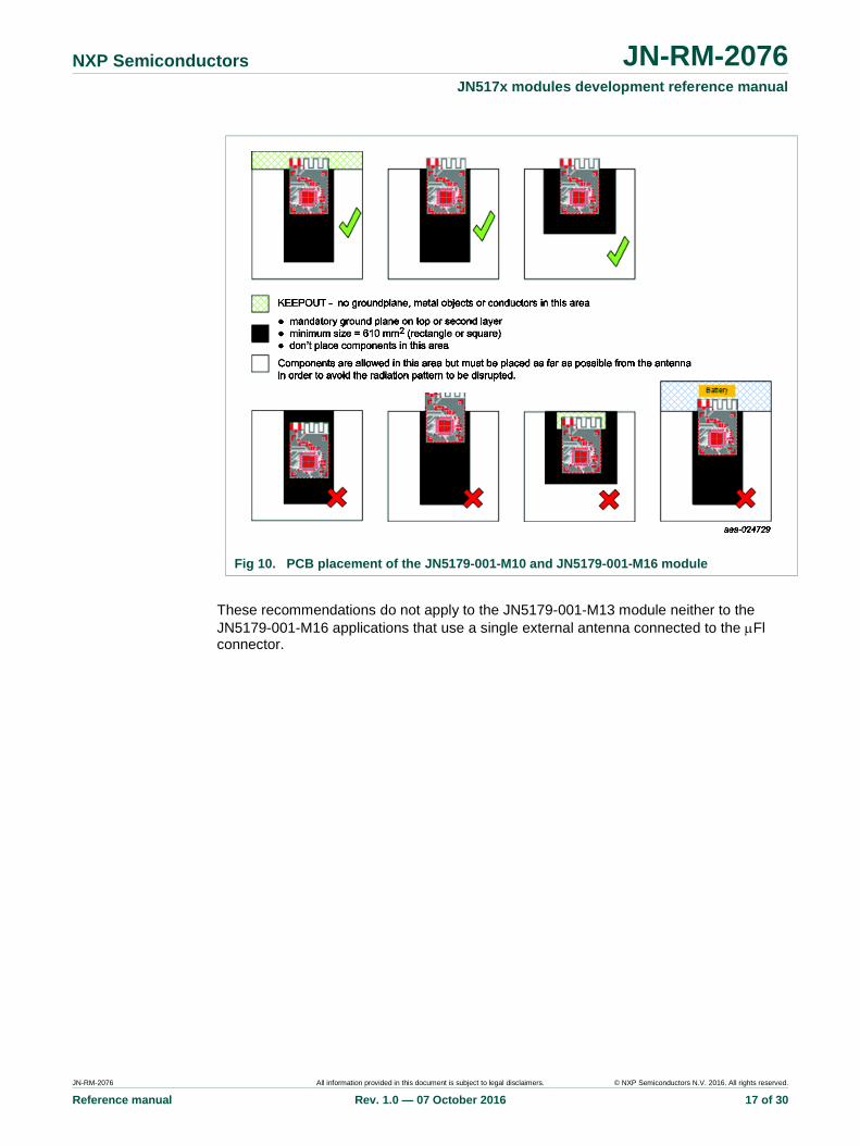
3.7 Optimal PCB placement of JN5179-001-M10 and JN5179-001-M16 modules The JN5179-001-M10 and JN5179-001-M16 modules feature an optimised, low-cost, integrated, printed PCB antenna. For size reduction no ground plane has been added between the antenna and the JN5179 chip. So an additional ground plane must be added on the main PCB beneath the module in order to ensure a good antenna efficiency. This ground plane can be a rectangle or a square with respect to 2 conditions: it must be as wide as the module (14.5 mm) and the area must be equal or greater than 610 mm2. See Fig 10 below for correct placement of the module.
The antenna has a vertically polarised near omnidirectional radiation pattern and up to 1.8 dBi of peak gain. On the antenna side the ground plane of the module must be vertically aligned with the ground plane of the main PCB. The area around the antenna must be kept clear of conductors or other metal objects by a minimum distance of 20 mm except the mandatory ground plane as indicated above. This is true for all layers of the PCB and not just the top layer. Any conductive objects close to the antenna could severely disrupt the antenna pattern resulting in deep nulls and high directivity in some directions.
The Fig 10 show various possible scenarios. The top 3 scenarios are correct - the ground plane must be placed beneath the JN5179-001-M10 or M16 module but it does not protrude beyond the edge of the top layer ground plane on the module PCB.
The bottom fours scenarios are incorrect – in the left-hand side there is ground plane underneath the antenna, in the middle-left example the ground planes of the main PCB and the module are not vertically aligned, in the middle-right there is insufficient clearance around the antenna, and in the right-hand example a battery’s metal casing is in the recommended ‘keep out’ area.
NXP Semiconductors JN-RM-2076 JN517x modules development reference manual
JN-RM-2076 All information provided in this document is subject to legal disclaimers. © NXP Semiconductors N.V. 2016. All rights reserved.
Reference manual Rev. 1.0 — 07 October 2016 17 of 30
Fig 10. PCB placement of the JN5179-001-M10 and JN5179-001-M16 module
These recommendations do not apply to the JN5179-001-M13 module neither to the
JN5179-001-M16 applications that use a single external antenna connected to the Fl connector.

NXP Semiconductors JN-RM-2076 JN517x modules development reference manual
JN-RM-2076 All information provided in this document is subject to legal disclaimers. © NXP Semiconductors N.V. 2016. All rights reserved.
Reference manual Rev. 1.0 — 07 October 2016 18 of 30
3.8 Manufacturing considerations The HVQFN package must be considered carefully when using reflow solder techniques.
Package footprint information can be found in the JN517x data sheet.
The decal is shown in Fig 11. The pad stacks used are 0.25 mm by 1 mm for the smaller pads, and a 6.4 mm square pad for the paddle.
Fig 11. Recommended PCB decal for HVQFN40 40-pin QFN
The solder mask used is shown in Fig 12. The pad stacks used are 0.25 mm by 1 mm for the smaller pads, and four 1.6 mm square pads to apply paste to the paddle. The solder paste mask has a thickness of 6-thou (0.152 mm). If the paste thickness needs to deviate from that used NXP then it may be necessary to change the number of pads that the paste is applied to. Paste thickness may be dictated by additional components used in a design.

NXP Semiconductors JN-RM-2076 JN517x modules development reference manual
JN-RM-2076 All information provided in this document is subject to legal disclaimers. © NXP Semiconductors N.V. 2016. All rights reserved.
Reference manual Rev. 1.0 — 07 October 2016 19 of 30
Fig 12. Solder paste mask for HVQFN40 40-pin QFN
Fig 13. Vias on the paddle of the HVQFN40 40-pin QFN
25 vias are applied to the paddle. These allow excess solder paste and heated air to be vented away from the device, preventing the device from being lifted during soldering. In addition, these vias ensure that a low impedance ground is maintained, which is vital for optimum RF performance.

NX
P S
em
ico
nd
uc
tors
JN
51
7x m
od
ule
s d
evelo
pm
en
t refe
ren
ce m
an
ual
JN
-RM
-207
6
Refe
ren
ce m
an
ual
JN
-RM
-2076
Rev. 1
.0 —
07 O
cto
be
r 2016
All in
form
atio
n p
rovid
ed in
this
docum
ent is
subje
ct to
legal d
iscla
imers
.
20 o
f 30
© N
XP
B.V
. 2016. A
ll rights
reserv
ed.
4. Check list schematic
Table 4. Schematic design-in check list
Check number Schematic design-in review check list Y/N/NR Customer comments and/or actions Check done by NXP Feedback
1 General
1.1 Have the schematics been checked
versus NXP reference schematics and
Application Notes?
1.2 Have the schematics been reviewed by
several people?
1.3 Does the application use non-standard
components?
1.4 Have the non-standard components
been qualified so that they can be used
in the application?
1.5 Are recommendations for layout/form
factor written on the schematics?
1.6 Are the components sized for the wanted
current drive capability?
1.7 Has the JN51XX symbol pinning been
checked and does it include the exposed
pad?
2 RF_IO
2.1 Is the characteristic impedance of the RF
input line 50 ohm over the full RF range?
2.2 Have components with the correct type
and value been connected to the RF port
of the JN51xx?
2.3 Is filtering/matching needed in front of
the RF input?
3 Crystal reference oscillator
3.1 Is the oscillator external configuration in
accordance with the Application Note
(i.e. capacitors, T° and 40 ppm)?
3.2 Has XTAL type been recommended by
NXP?

NX
P S
em
ico
nd
uc
tors
JN
51
7x m
od
ule
s d
evelo
pm
en
t refe
ren
ce m
an
ual
JN
-RM
-207
6
Refe
ren
ce m
an
ual
JN
-RM
-2076
Rev. 1
.0 —
07 O
cto
be
r 2016
All in
form
atio
n p
rovid
ed in
this
docum
ent is
subje
ct to
legal d
iscla
imers
.
21 o
f 30
© N
XP
B.V
. 2016. A
ll rights
reserv
ed.
Check number Schematic design-in review check list Y/N/NR Customer comments and/or actions Check done by NXP Feedback
4 Power supply
4.1 Have all the VDD pins been connected?
4.2 Are the power supply regulators well
sized?
4.3 Has the decoupling of the supply
regulators output been implemented?
4.4 Have the power supply pins of the IC been properly decoupled (according to the Application Note and Reference Design schematics?)
4.5 Has the exposed die pad been
connected to GND?
5 DIO
5.1 Has the compatibility of the logic levels
with other components been checked?
5.2 Does the max source/sink current fit the
application?
6 ADC
6.1 Does the ADC characteristics fit the
application?
7 Biasing
7.1 Is the Rbias resistor value 43 k at 1%?
8 VCO tune
8.1 Has the VCO Tune pin left open? (pin 7
on JN516x). Not applicable for JN517x.
9 Programming and debug
9.1 Has the flash programming connector
been connected to the correct I/O on the
microcontroller?
9.2 Has a connector been added that allows
the microcontroller to be put into
programming mode? (RESET_N and
SPIMISO pins)
9.3 Is RESET_N properly connected?

NX
P S
em
ico
nd
uc
tors
JN
51
7x m
od
ule
s d
evelo
pm
en
t refe
ren
ce m
an
ual
JN
-RM
-207
6
Refe
ren
ce m
an
ual
JN
-RM
-2076
Rev. 1
.0 —
07 O
cto
be
r 2016
All in
form
atio
n p
rovid
ed in
this
docum
ent is
subje
ct to
legal d
iscla
imers
.
22 o
f 30
© N
XP
B.V
. 2016. A
ll rights
reserv
ed.
Check number Schematic design-in review check list Y/N/NR Customer comments and/or actions Check done by NXP Feedback
9.4 Add a test point at a unused DIO in order
a trigger signal can be output from the
pin for sensitivity measurements
9.5 For printed antenna: is the RF line
implemented in order to debug JN51xx
on one side and antenna on the other
side?
9.6 If I2C-bus used, are the I2C-bus lines
pulled up?
9.7 Check loading on SPICLK pin. Pin is
input during reset and device could enter
JTAG programming mode
10 External memory
10.1 Has the correct type of external flash
memory been used and is it connected
to the microcontroller correctly?
10.2 Has the flash memory symbol pinning
been checked?
NX
P S
em
ico
nd
uc
tors
JN
51
7x m
od
ule
s d
evelo
pm
en
t refe
ren
ce m
an
ual
JN
-RM
-207
6
Refe
ren
ce m
an
ual
JN
-RM
-2076
Rev. 1
.0 —
07 O
cto
be
r 2016
All in
form
atio
n p
rovid
ed in
this
docum
ent is
subje
ct to
legal d
iscla
imers
.
23 o
f 30
© N
XP
B.V
. 2016. A
ll rights
reserv
ed.
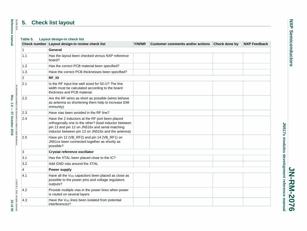
5. Check list layout
Table 5. Layout design-in check list
Check number Layout design-in review check list Y/N/NR Customer comments and/or actions Check done by NXP Feedback
1 General
1.1 Has the layout been checked versus NXP reference
board?
1.2 Has the correct PCB material been specified?
1.3 Have the correct PCB thicknesses been specified?
2 RF_IO
2.1 Is the RF input line well sized for 50 ? The line
width must be calculated according to the board
thickness and PCB material.
2.2 Are the RF wires as short as possible (wires behave
as antenna so shortening them help to increase EMI
immunity)
2.3 Have vias been avoided in the RF line?
2.4 Have the 2 inductors at the RF port been placed
orthogonally one to the other? (load inductor between
pin 13 and pin 12 on JN516x and serial matching
inductor between pin 13 on JN516x and the antenna)
2.5 Have pin 12 (VB_RF2) and pin 14 (VB_RF1) on
JN51xx been connected together as shortly as
possible?
3 Crystal reference oscillator
3.1 Has the XTAL been placed close to the IC?
3.2 Add GND vias around the XTAL
4 Power supply
4.1 Have all the VDD capacitors been placed as close as
possible to the power pins and voltage regulators
outputs?
4.2 Provide multiple vias in the power lines when power
is routed on several layers
4.3 Have the VDD lines been isolated from potential interferences?

NX
P S
em
ico
nd
uc
tors
JN
51
7x m
od
ule
s d
evelo
pm
en
t refe
ren
ce m
an
ual
JN
-RM
-207
6
Refe
ren
ce m
an
ual
JN
-RM
-2076
Rev. 1
.0 —
07 O
cto
be
r 2016
All in
form
atio
n p
rovid
ed in
this
docum
ent is
subje
ct to
legal d
iscla
imers
.
24 o
f 30
© N
XP
B.V
. 2016. A
ll rights
reserv
ed.
Check number Layout design-in review check list Y/N/NR Customer comments and/or actions Check done by NXP Feedback
4.5 Is GND plane continuous around and near all
signals?
4.5 Has the die pad been properly connected to GND?
4.6 Are vias implemented in the die pad?
5 Antenna
5.1 Has the antenna placement been discussed?
6 EMC and misc.
6.1 Has the number of layers been clearly discussed?
6.2 In case more than 2 layers are used, does one layer
act as a continuous ground plane (GND reference
plane)?
6.3 Are numerous vias added near capacitor, near
fingers,…?
6.4 Remove small GND areas and isolated fingers that
cannot be connected to the reference GND plane
with a via.
6.5 Have silk screens been added with relevant
information? (components ref, logo, board name…)
6.6 Are all silkscreen texts readable when the board is
populated?
6.7 Have traces been avoided below noisy or sensitive
components?
6.8 Check that traces do not cut across power or ground
planes unnecessarily.
6.9 Is the JN51XX footprint strictly similar to the NXP
reference?
6.10 If more than 2 layers are used, the inner layers must
be left empty below the RF components and the
antenna
6.11 Each connection between a component and GND
must be doubled with a via to the GND plane.
6.12 Is GND plane clearance of .3 mm on the PCB edge
respected?
6.13 Have the soldering/non soldering areas been
respected?

NX
P S
em
ico
nd
uc
tors
JN
51
7x m
od
ule
s d
evelo
pm
en
t refe
ren
ce m
an
ual
JN
-RM
-207
6
Refe
ren
ce m
an
ual
JN
-RM
-2076
Rev. 1
.0 —
07 O
cto
be
r 2016
All in
form
atio
n p
rovid
ed in
this
docum
ent is
subje
ct to
legal d
iscla
imers
.
25 o
f 30
© N
XP
B.V
. 2016. A
ll rights
reserv
ed.
Check number Layout design-in review check list Y/N/NR Customer comments and/or actions Check done by NXP Feedback
Is solder resist layer check in the empty area?"
6.14 If sold unit is a module is a CAN/shield implemented?

NXP Semiconductors JN-RM-2076 JN517x modules development reference manual
JN-RM-2076 All information provided in this document is subject to legal disclaimers. © NXP B.V. 2016. All rights reserved.
Reference manual Rev. 1.0 — 07 October 2016 26 of 30
6. Abbreviations
Table 6. Abbreviations
Acronym Description
EMC Electro Magnetic Compatibility
ETSI European Telecommunications Standards Institute
FCC Federal Communications Commission
PAN Personal Area Network
PCB Printed Circuit Board
RF Radio Frequency
SPI-bus Serial Peripheral Interface-bus
TQFN Thin Quad Flat No-lead
WPAN Wireless Personal Area Network
7. References
JN517X Datasheet – IEEE802.15.4 Wireless Microcontroller
JN517X-modules Datasheet – ZigBee Pro and IEEE802.15.4 modules

Erro
r!
Unkn
ow
n
do
cu
me
nt
pro
pe
rty
na
me
.
Erro
r! Unkno
wn d
ocum
ent p
roperty
nam
e.
Erro
r! Un
kn
ow
n d
ocu
me
nt p
rop
erty
na
me
.
NXP Semiconductors JN-RM-2076 JN517x modules development reference manual
JN-RM-2076 All information provided in this document is subject to legal disclaimers. © NXP Semiconductors N.V. 2016. All rights reserved.
Reference manual Rev. 1.0 — 07 October 2016 27 of 30
8. Legal information
8.1 Definitions Draft — The document is a draft version only. The content is still under
internal review and subject to formal approval, which may result in
modifications or additions. NXP Semiconductors does not give any
representations or warranties as to the accuracy or completeness of
information included herein and shall have no liability for the consequences
of use of such information.
8.2 Disclaimers Limited warranty and liability — Information in this document is believed to
be accurate and reliable. However, NXP Semiconductors does not give any
representations or warranties, expressed or implied, as to the accuracy or
completeness of such information and shall have no liability for the
consequences of use of such information. NXP Semiconductors takes no
responsibility for the content in this document if provided by an information
source outside of NXP Semiconductors.
In no event shall NXP Semiconductors be liable for any indirect, incidental,
punitive, special or consequential damages (including - without limitation -
lost profits, lost savings, business interruption, costs related to the removal or
replacement of any products or rework charges) whether or not such
damages are based on tort (including negligence), warranty, breach of
contract or any other legal theory.
Notwithstanding any damages that customer might incur for any reason
whatsoever, NXP Semiconductors’ aggregate and cumulative liability
towards customer for the products described herein shall be limited in
accordance with the Terms and conditions of commercial sale of NXP
Semiconductors.
Right to make changes — NXP Semiconductors reserves the right to make
changes to information published in this document, including without
limitation specifications and product descriptions, at any time and without
notice. This document supersedes and replaces all information supplied prior
to the publication hereof.
Suitability for use — NXP Semiconductors products are not designed,
authorized or warranted to be suitable for use in life support, life-critical or
safety-critical systems or equipment, nor in applications where failure or
malfunction of an NXP Semiconductors product can reasonably be expected
to result in personal injury, death or severe property or environmental
damage. NXP Semiconductors and its suppliers accept no liability for
inclusion and/or use of NXP Semiconductors products in such equipment or
applications and therefore such inclusion and/or use is at the customer’s
own risk.
Applications — Applications that are described herein for any of these
products are for illustrative purposes only. NXP Semiconductors makes no
representation or warranty that such applications will be suitable for the
specified use without further testing or modification.
Customers are responsible for the design and operation of their applications
and products using NXP Semiconductors products, and NXP
Semiconductors accepts no liability for any assistance with applications or
customer product design. It is customer’s sole responsibility to determine
whether the NXP Semiconductors product is suitable and fit for the
customer’s applications and products planned, as well as for the planned
application and use of customer’s third party customer(s). Customers should
provide appropriate design and operating safeguards to minimize the risks
associated with their applications and products.
NXP Semiconductors does not accept any liability related to any default,
damage, costs or problem which is based on any weakness or default in the
customer’s applications or products, or the application or use by customer’s
third party customer(s). Customer is responsible for doing all necessary
testing for the customer’s applications and products using NXP
Semiconductors products in order to avoid a default of the applications and
the products or of the application or use by customer’s third party
customer(s). NXP does not accept any liability in this respect.
Export control — This document as well as the item(s) described herein
may be subject to export control regulations. Export might require a prior
authorization from competent authorities.
Translations — A non-English (translated) version of a document is for
reference only. The English version shall prevail in case of any discrepancy
between the translated and English versions.
Evaluation products — This product is provided on an “as is” and “with all
faults” basis for evaluation purposes only. NXP Semiconductors, its affiliates
and their suppliers expressly disclaim all warranties, whether express,
implied or statutory, including but not limited to the implied warranties of non-
infringement, merchantability and fitness for a particular purpose. The entire
risk as to the quality, or arising out of the use or performance, of this product
remains with customer.
In no event shall NXP Semiconductors, its affiliates or their suppliers be
liable to customer for any special, indirect, consequential, punitive or
incidental damages (including without limitation damages for loss of
business, business interruption, loss of use, loss of data or information, and
the like) arising out the use of or inability to use the product, whether or not
based on tort (including negligence), strict liability, breach of contract, breach
of warranty or any other theory, even if advised of the possibility of such
damages.
Notwithstanding any damages that customer might incur for any reason
whatsoever (including without limitation, all damages referenced above and
all direct or general damages), the entire liability of NXP Semiconductors, its
affiliates and their suppliers and customer’s exclusive remedy for all of the
foregoing shall be limited to actual damages incurred by customer based on
reasonable reliance up to the greater of the amount actually paid by
customer for the product or five dollars (US$5.00). The foregoing limitations,
exclusions and disclaimers shall apply to the maximum extent permitted by
applicable law, even if any remedy fails of its essential purpose.
8.3 Patents Notice is herewith given that the subject device uses one or more of the
following patents and that each of these patents may have corresponding
patents in other jurisdictions.
8.4 Trademarks Notice: All referenced brands, product names, service names and
trademarks are property of their respective owners.
NXP Semiconductors JN-RM-2076 JN517x modules development reference manual
JN-RM-2076 All information provided in this document is subject to legal disclaimers. © NXP Semiconductors N.V. 2016. All rights reserved.
Reference manual Rev. 1.0 — 07 October 2016 28 of 30
9. List of figures
Fig 1. PGM connection to the module ......................... 5 Fig 2. Screening can drawing ..................................... 6 Fig 3. Edge connector details ..................................... 7 Fig 4. PCB stack-up .................................................... 8 Fig 5. RF layout considerations................................. 10 Fig 6. Matching network and low-pass Pi filter .......... 11 Fig 7. Matching network, FEM and low-pass Pi filter 11 Fig 8. JN5179-001-M10 and JN5179-001-M13
matching network and low-pass filter layout.... 12 Fig 9. JN5179-001-M16 matching network ............... 12 Fig 10. PCB placement of the JN5179-001-M10 and
JN5179-001-M16 module................................ 17 Fig 11. Recommended PCB decal for HVQFN40 40-pin
QFN ................................................................ 18 Fig 12. Solder paste mask for HVQFN40 40-pin QFN 19 Fig 13. Vias on the paddle of the HVQFN40 40-pin QFN
........................................................................ 19

NXP Semiconductors JN-RM-2076 JN517x modules development reference manual
JN-RM-2076 All information provided in this document is subject to legal disclaimers. © NXP Semiconductors N.V. 2016. All rights reserved.
Reference manual Rev. 1.0 — 07 October 2016 29 of 30
10. List of tables
Table 1. Modules references .......................................... 4 Table 2. Layout requirements and components list for
JN5179-001-M10 and JN5179-001-M13 ......... 13 Table 3. Layout requirements and components list for
JN5179-001-M16 ............................................ 14 Table 4. Schematic design-in check list ........................ 20 Table 5. Layout design-in check list .............................. 23 Table 6. Abbreviations .................................................. 26

NXP Semiconductors JN-RM-2076 JN517x modules development reference manual
Please be aware that important notices concerning this document and the product(s) described herein, have been included in the section 'Legal information'.
© NXP Semiconductors N.V. 2016. All rights reserved.
For more information, please visit: http://www.nxp.com
Date of release: 07 October 2016
Document identifier: JN-RM-2076
11. Contents
1. Introduction ......................................................... 3 2. Reference Design ................................................ 3 2.1 Entering programming mode .............................. 5 2.2 Screening can .................................................... 5 3. Design considerations ........................................ 7 3.1 PCB requirements .............................................. 7 3.1.1 Common features (all modules) ......................... 7 3.1.2 Modules – PCB stack-up .................................... 8 3.2 Supply decoupling .............................................. 8 3.3 Reference oscillator ........................................... 8 3.3.1 Reference oscillator requirements ...................... 8 3.3.2 Specific layout considerations ............................ 9 3.4 RF considerations .............................................. 9 3.4.1 RF matching components and controlled
impedances ...................................................... 10 3.4.2 RF low-pass filter ............................................. 11 3.4.3 Layout .............................................................. 12 3.5 Other layout requirements ................................ 12 3.6 Ground planes .................................................. 15 3.7 Optimal PCB placement of JN5179-001-M10 and
JN5179-001-M16 modules ............................... 16 3.8 Manufacturing considerations .......................... 18 4. Check list schematic ......................................... 20 5. Check list layout ................................................ 23 6. Abbreviations .................................................... 26 7. References ......................................................... 26 8. Legal information .............................................. 27 8.1 Definitions ........................................................ 27 8.2 Disclaimers....................................................... 27 8.3 Patents ............................................................. 27 8.4 Trademarks ...................................................... 27 9. List of figures ..................................................... 28 10. List of tables ...................................................... 29 11. Contents ............................................................. 30