JEDEC PUBLICATION 95 - Analog, Embedded … Publication 95 Microelectronic Package Standard SZZA006...
23
1999 Application Report
Transcript of JEDEC PUBLICATION 95 - Analog, Embedded … Publication 95 Microelectronic Package Standard SZZA006...

����� ���� ����� ���� ����� ����� � ���� �������
1999
ApplicationReport

Printed in U.S.A.0199
SZZA006
1
JEDEC Publication 95Microelectronic Package Standard
SZZA006January 1999
2
IMPORTANT NOTICE
Texas Instruments and its subsidiaries (TI) reserve the right to make changes to their productsor to discontinue any product or service without notice, and advise customers to obtain the latestversion of relevant information to verify, before placing orders, that information being relied onis current and complete. All products are sold subject to the terms and conditions of sale suppliedat the time of order acknowledgement, including those pertaining to warranty, patentinfringement, and limitation of liability.
TI warrants performance of its semiconductor products to the specifications applicable at thetime of sale in accordance with TI’s standard warranty. Testing and other quality controltechniques are utilized to the extent TI deems necessary to support this warranty. Specific testingof all parameters of each device is not necessarily performed, except those mandated bygovernment requirements.
CERTAIN APPLICATIONS USING SEMICONDUCTOR PRODUCTS MAY INVOLVEPOTENTIAL RISKS OF DEATH, PERSONAL INJURY, OR SEVERE PROPERTY ORENVIRONMENTAL DAMAGE (“CRITICAL APPLICATIONS”). TI SEMICONDUCTORPRODUCTS ARE NOT DESIGNED, AUTHORIZED, OR WARRANTED TO BE SUITABLE FORUSE IN LIFE-SUPPORT DEVICES OR SYSTEMS OR OTHER CRITICAL APPLICATIONS.INCLUSION OF TI PRODUCTS IN SUCH APPLICATIONS IS UNDERSTOOD TO BE FULLYAT THE CUSTOMER’S RISK.
In order to minimize risks associated with the customer’s applications, adequate design andoperating safeguards must be provided by the customer to minimize inherent or proceduralhazards.
TI assumes no liability for applications assistance or customer product design. TI does notwarrant or represent that any license, either express or implied, is granted under any patent right,copyright, mask work right, or other intellectual property right of TI covering or relating to anycombination, machine, or process in which such semiconductor products or services might beor are used. TI’s publication of information regarding any third party’s products or services doesnot constitute TI’s approval, warranty or endorsement thereof.
Copyright 1999, Texas Instruments Incorporated

iii
ContentsTitle Page
Abstract 1. . . . . . . . . . . . . . . . . . . . . . . . . . . . . . . . . . . . . . . . . . . . . . . . . . . . . . . . . . . . . . . . . . . . . . . . . . . . . . . . . . . . . . . . . . .
What Is EIA/JEDEC? 1. . . . . . . . . . . . . . . . . . . . . . . . . . . . . . . . . . . . . . . . . . . . . . . . . . . . . . . . . . . . . . . . . . . . . . . . . . . . . . .
What Is Publication 95? 3. . . . . . . . . . . . . . . . . . . . . . . . . . . . . . . . . . . . . . . . . . . . . . . . . . . . . . . . . . . . . . . . . . . . . . . . . . . . . Purpose 3. . . . . . . . . . . . . . . . . . . . . . . . . . . . . . . . . . . . . . . . . . . . . . . . . . . . . . . . . . . . . . . . . . . . . . . . . . . . . . . . . . . . . . . Registered Outlines vs Standard Outlines 3. . . . . . . . . . . . . . . . . . . . . . . . . . . . . . . . . . . . . . . . . . . . . . . . . . . . . . . . . . . . How Are Documents Controlled? 4. . . . . . . . . . . . . . . . . . . . . . . . . . . . . . . . . . . . . . . . . . . . . . . . . . . . . . . . . . . . . . . . . . How Are Changes Made? 5. . . . . . . . . . . . . . . . . . . . . . . . . . . . . . . . . . . . . . . . . . . . . . . . . . . . . . . . . . . . . . . . . . . . . . . . . Does Our Package Outline Conform to JEDEC? 5. . . . . . . . . . . . . . . . . . . . . . . . . . . . . . . . . . . . . . . . . . . . . . . . . . . . . . .
What Is Contained in Publication 95? 5. . . . . . . . . . . . . . . . . . . . . . . . . . . . . . . . . . . . . . . . . . . . . . . . . . . . . . . . . . . . . . . . . . Contents 5. . . . . . . . . . . . . . . . . . . . . . . . . . . . . . . . . . . . . . . . . . . . . . . . . . . . . . . . . . . . . . . . . . . . . . . . . . . . . . . . . . . . . . Requirements for Document Registration 5. . . . . . . . . . . . . . . . . . . . . . . . . . . . . . . . . . . . . . . . . . . . . . . . . . . . . . . . . . . . Definitions and Symbology 5. . . . . . . . . . . . . . . . . . . . . . . . . . . . . . . . . . . . . . . . . . . . . . . . . . . . . . . . . . . . . . . . . . . . . . . Various Registered-Outline Types 6. . . . . . . . . . . . . . . . . . . . . . . . . . . . . . . . . . . . . . . . . . . . . . . . . . . . . . . . . . . . . . . . . . Various Standard-Outline Types 6. . . . . . . . . . . . . . . . . . . . . . . . . . . . . . . . . . . . . . . . . . . . . . . . . . . . . . . . . . . . . . . . . . . . How to Access Publication 95 on the Web 6. . . . . . . . . . . . . . . . . . . . . . . . . . . . . . . . . . . . . . . . . . . . . . . . . . . . . . . . . . .
How to Find a Registration or Standard Number 7. . . . . . . . . . . . . . . . . . . . . . . . . . . . . . . . . . . . . . . . . . . . . . . . . . . . . . . . Option 1 7. . . . . . . . . . . . . . . . . . . . . . . . . . . . . . . . . . . . . . . . . . . . . . . . . . . . . . . . . . . . . . . . . . . . . . . . . . . . . . . . . . . . . . Option 2 8. . . . . . . . . . . . . . . . . . . . . . . . . . . . . . . . . . . . . . . . . . . . . . . . . . . . . . . . . . . . . . . . . . . . . . . . . . . . . . . . . . . . . . Option 3 8. . . . . . . . . . . . . . . . . . . . . . . . . . . . . . . . . . . . . . . . . . . . . . . . . . . . . . . . . . . . . . . . . . . . . . . . . . . . . . . . . . . . . . Option 4 9. . . . . . . . . . . . . . . . . . . . . . . . . . . . . . . . . . . . . . . . . . . . . . . . . . . . . . . . . . . . . . . . . . . . . . . . . . . . . . . . . . . . . . Option 5 9. . . . . . . . . . . . . . . . . . . . . . . . . . . . . . . . . . . . . . . . . . . . . . . . . . . . . . . . . . . . . . . . . . . . . . . . . . . . . . . . . . . . . . Search Procedure 9. . . . . . . . . . . . . . . . . . . . . . . . . . . . . . . . . . . . . . . . . . . . . . . . . . . . . . . . . . . . . . . . . . . . . . . . . . . . . . . Guides for Designers 11. . . . . . . . . . . . . . . . . . . . . . . . . . . . . . . . . . . . . . . . . . . . . . . . . . . . . . . . . . . . . . . . . . . . . . . . . . .
Summary 11. . . . . . . . . . . . . . . . . . . . . . . . . . . . . . . . . . . . . . . . . . . . . . . . . . . . . . . . . . . . . . . . . . . . . . . . . . . . . . . . . . . . . . . . .
Glossary 13. . . . . . . . . . . . . . . . . . . . . . . . . . . . . . . . . . . . . . . . . . . . . . . . . . . . . . . . . . . . . . . . . . . . . . . . . . . . . . . . . . . . . . . . .
Acknowledgment 13. . . . . . . . . . . . . . . . . . . . . . . . . . . . . . . . . . . . . . . . . . . . . . . . . . . . . . . . . . . . . . . . . . . . . . . . . . . . . . . . . .
Bibliography 13. . . . . . . . . . . . . . . . . . . . . . . . . . . . . . . . . . . . . . . . . . . . . . . . . . . . . . . . . . . . . . . . . . . . . . . . . . . . . . . . . . . . . .
Appendix A 14. . . . . . . . . . . . . . . . . . . . . . . . . . . . . . . . . . . . . . . . . . . . . . . . . . . . . . . . . . . . . . . . . . . . . . . . . . . . . . . . . . . . . . .

iv
List of IllustrationsFigure Title Page
1 EIA Web Page 1. . . . . . . . . . . . . . . . . . . . . . . . . . . . . . . . . . . . . . . . . . . . . . . . . . . . . . . . . . . . . . . . . . . . . . . . . . . . . . .
2 JEDEC Web Page 2. . . . . . . . . . . . . . . . . . . . . . . . . . . . . . . . . . . . . . . . . . . . . . . . . . . . . . . . . . . . . . . . . . . . . . . . . . . .
3 Access to Publication 95 3. . . . . . . . . . . . . . . . . . . . . . . . . . . . . . . . . . . . . . . . . . . . . . . . . . . . . . . . . . . . . . . . . . . . . . .
4 Publication 95 Web Page 4. . . . . . . . . . . . . . . . . . . . . . . . . . . . . . . . . . . . . . . . . . . . . . . . . . . . . . . . . . . . . . . . . . . . . . .
5 Publication 95 Web-Page Extension 4. . . . . . . . . . . . . . . . . . . . . . . . . . . . . . . . . . . . . . . . . . . . . . . . . . . . . . . . . . . . . .
6 Master Index 7. . . . . . . . . . . . . . . . . . . . . . . . . . . . . . . . . . . . . . . . . . . . . . . . . . . . . . . . . . . . . . . . . . . . . . . . . . . . . . . .
7 Other Sections (Design Guides) 8. . . . . . . . . . . . . . . . . . . . . . . . . . . . . . . . . . . . . . . . . . . . . . . . . . . . . . . . . . . . . . . . .
8 Standard Practices and Procedures (SPP) 8. . . . . . . . . . . . . . . . . . . . . . . . . . . . . . . . . . . . . . . . . . . . . . . . . . . . . . . . . .
9 Microelectronic Outlines (MO) 9. . . . . . . . . . . . . . . . . . . . . . . . . . . . . . . . . . . . . . . . . . . . . . . . . . . . . . . . . . . . . . . . . .
10 Index of MOs by Family 10. . . . . . . . . . . . . . . . . . . . . . . . . . . . . . . . . . . . . . . . . . . . . . . . . . . . . . . . . . . . . . . . . . . . . .
11 Listing of Ball Grid Array Registrations 10. . . . . . . . . . . . . . . . . . . . . . . . . . . . . . . . . . . . . . . . . . . . . . . . . . . . . . . . . .
A–1 Example of a Registered-Outline Drawing Top Sheet 14. . . . . . . . . . . . . . . . . . . . . . . . . . . . . . . . . . . . . . . . . . . . . . .
A–2 Example of a Standard-Outline Drawing Top Sheet 15. . . . . . . . . . . . . . . . . . . . . . . . . . . . . . . . . . . . . . . . . . . . . . . . .
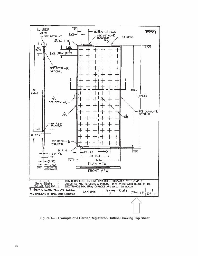
A–3 Example of a Carrier Registered-Outline Drawing Top Sheet 16. . . . . . . . . . . . . . . . . . . . . . . . . . . . . . . . . . . . . . . . .
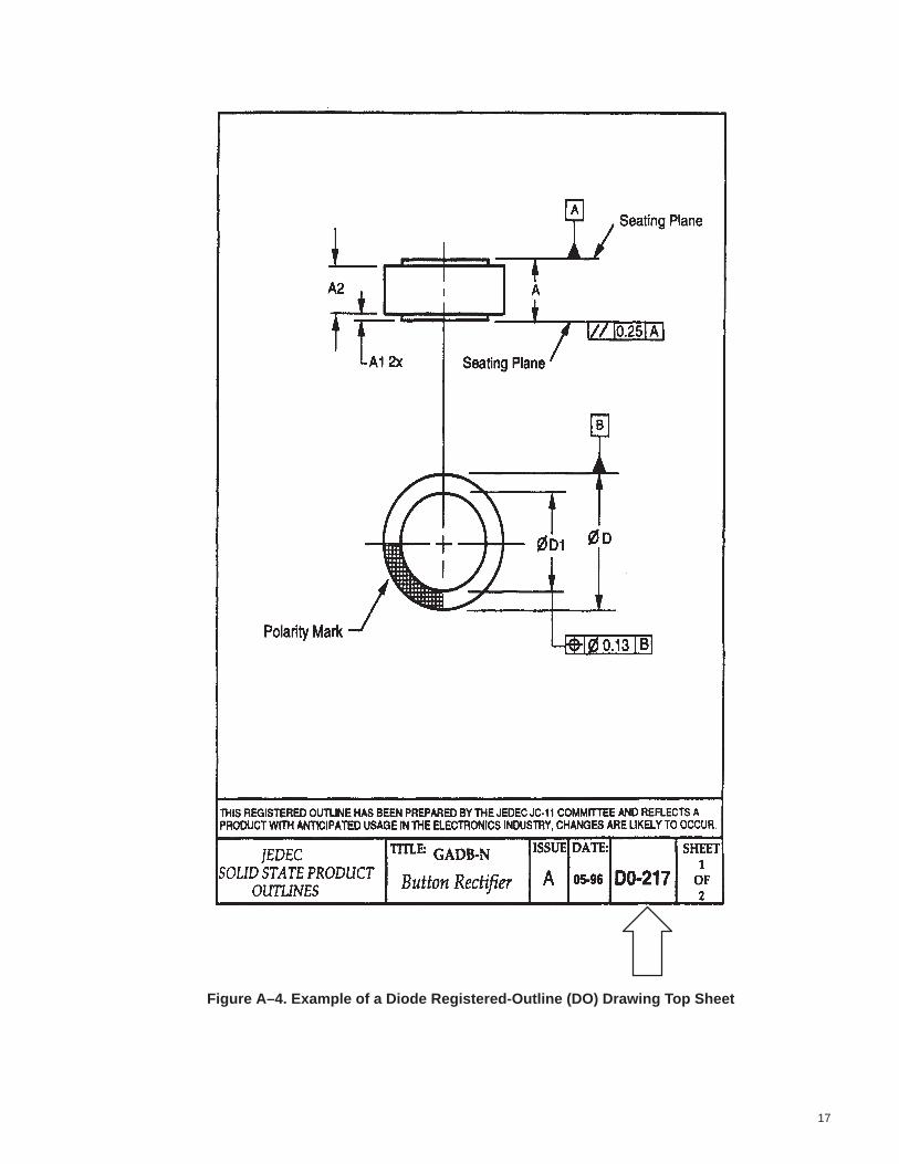
A–4 Example of a Diode Registered-Outline (DO) Drawing Top Sheet 17. . . . . . . . . . . . . . . . . . . . . . . . . . . . . . . . . . . . .
1
Abstract
Many electronics companies have joined the Joint Electron Device Engineering Council (JEDEC) and the JC-11 Mechanical(Package Outline) Standardization committee to gain further understanding of industry package standards and to register theirproduct lines. As a member of JC-11, the company receives a hardcopy of Publication 95 that generally is in the custody ofthe committee member. The publication is updated and maintained by the member or the alternate. The JC-11 member, oralternate, often is contacted for information, a drawing copy, or instructions for registering a package with JEDEC.
JEDEC provides free access to Publication 95 on the JEDEC web page. This document is intended to familiarize the readerwith the JC-11 procedures, requirements for registration, and how to locate and use Publication 95. The available informationis useful to packaging engineers, component engineers, product engineers, end users, designers, and marketing personnel.
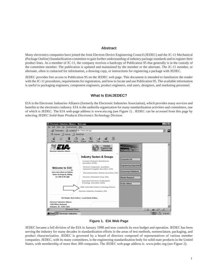
What Is EIA/JEDEC?
EIA is the Electronic Industries Alliance (formerly the Electronic Industries Association), which provides many services andbenefits to the electronics industry. EIA is the umbrella organization for many standardization activities and committees, oneof which is JEDEC. The EIA web-page address is www.eia.org (see Figure 1) . JEDEC can be accessed from this page byselecting JEDEC Solid-State Products Electronics Technology Division.
Figure 1. EIA Web Page
JEDEC became a full division of the EIA in January 1998 and now controls its own budget and operation. JEDEC has beenserving the industry for many decades in standardization efforts in the areas of test methods, nomenclature, packaging, andproduct characterization. JEDEC is governed by a board of directors composed of representatives of various membercompanies. JEDEC, with its many committees, is the engineering standardization body for solid-state products in the UnitedStates, with membership of more then 300 companies. The JEDEC web-page address is www.jedec.org (see Figure 2).
2
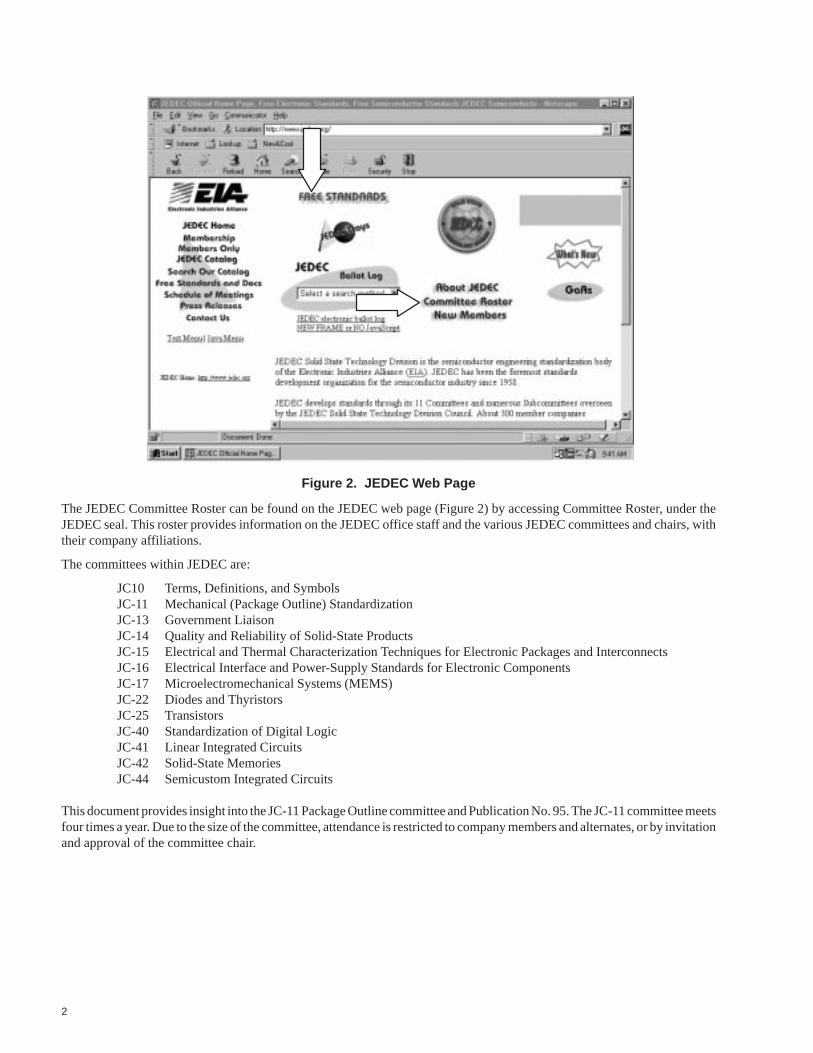
Figure 2. JEDEC Web Page
The JEDEC Committee Roster can be found on the JEDEC web page (Figure 2) by accessing Committee Roster, under theJEDEC seal. This roster provides information on the JEDEC office staff and the various JEDEC committees and chairs, withtheir company affiliations.
The committees within JEDEC are:
JC10 Terms, Definitions, and SymbolsJC-11 Mechanical (Package Outline) StandardizationJC-13 Government LiaisonJC-14 Quality and Reliability of Solid-State ProductsJC-15 Electrical and Thermal Characterization Techniques for Electronic Packages and InterconnectsJC-16 Electrical Interface and Power-Supply Standards for Electronic ComponentsJC-17 Microelectromechanical Systems (MEMS)JC-22 Diodes and ThyristorsJC-25 TransistorsJC-40 Standardization of Digital LogicJC-41 Linear Integrated CircuitsJC-42 Solid-State MemoriesJC-44 Semicustom Integrated Circuits
This document provides insight into the JC-11 Package Outline committee and Publication No. 95. The JC-11 committee meetsfour times a year. Due to the size of the committee, attendance is restricted to company members and alternates, or by invitationand approval of the committee chair.
3
What Is Publication 95?
Purpose
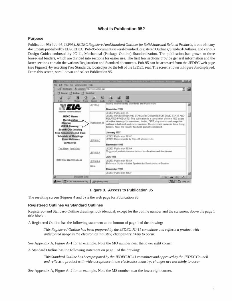
Publication 95 (Pub-95, JEP95), JEDEC Registered and Standard Outlines for Solid State and Related Products, is one of manydocuments published by EIA/JEDEC. Pub-95 documents several-hundred Registered Outlines, Standard Outlines, and variousDesign Guides endorsed by JC-11, Mechanical (Package Outline) Standardization. The publication has grown to threeloose-leaf binders, which are divided into sections for easier use. The first few sections provide general information and thelatter sections contain the various Registration and Standard documents. Pub-95 can be accessed from the JEDEC web page(see Figure 2) by selecting Free Standards, located just to the left of the JEDEC seal. The screen shown in Figure 3 is displayed.From this screen, scroll down and select Publication 95.
Figure 3. Access to Publication 95
The resulting screen (Figures 4 and 5) is the web page for Publication 95.
Registered Outlines vs Standard Outlines
Registered- and Standard-Outline drawings look identical, except for the outline number and the statement above the page 1title block.
A Registered Outline has the following statement at the bottom of page 1 of the drawing:
This Registered Outline has been prepared by the JEDEC JC-11 committee and reflects a product withanticipated usage in the electronics industry; changes are likely to occur.
See Appendix A, Figure A–1 for an example. Note the MO number near the lower right corner.
A Standard Outline has the following statement on page 1 of the drawing:
This Standard Outline has been prepared by the JEDEC JC-11 committee and approved by the JEDEC Counciland reflects a product with wide acceptance in the electronics industry; changes are not likely to occur.
See Appendix A, Figure A–2 for an example. Note the MS number near the lower right corner.
4
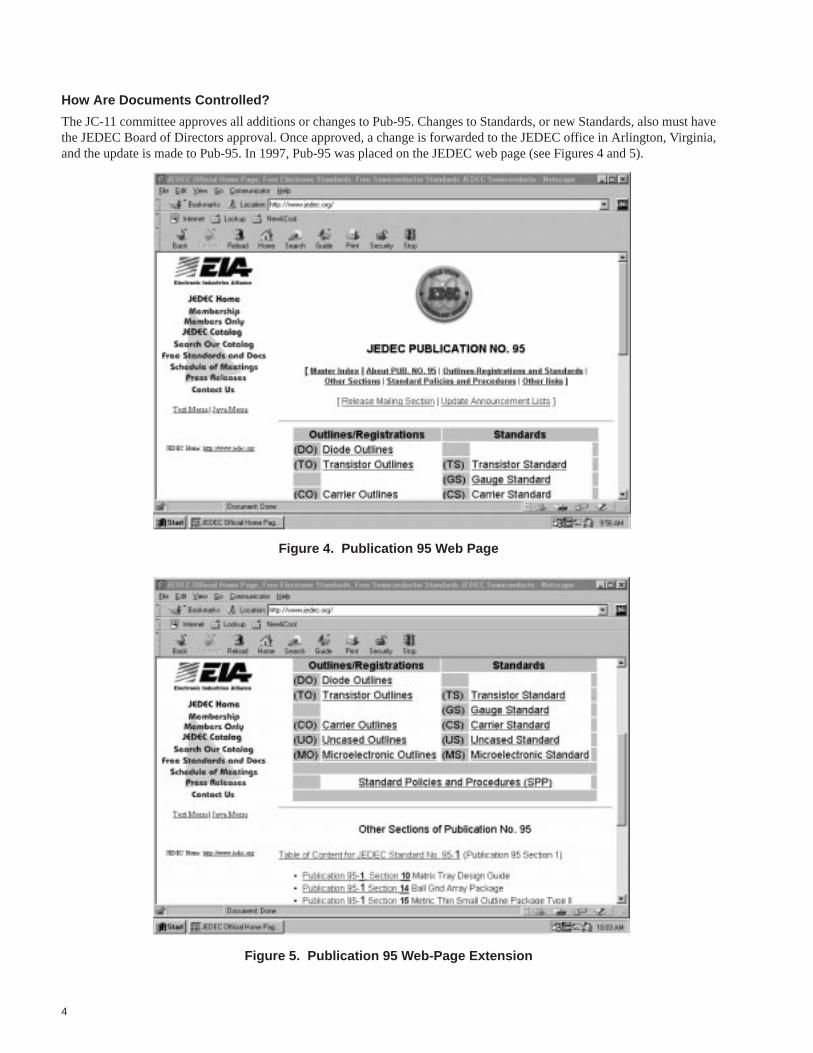
How Are Documents Controlled?
The JC-11 committee approves all additions or changes to Pub-95. Changes to Standards, or new Standards, also must havethe JEDEC Board of Directors approval. Once approved, a change is forwarded to the JEDEC office in Arlington, Virginia,and the update is made to Pub-95. In 1997, Pub-95 was placed on the JEDEC web page (see Figures 4 and 5).
Figure 4. Publication 95 Web Page
Figure 5. Publication 95 Web-Page Extension
5
How Are Changes Made?
Any JC-11 member company can propose a new Registration or Registration change. All proposals approved for ballot musthave a two-thirds affirmative vote before being published. Organizations within a company should contact their JC-11 memberfor needed changes or registrations. If a company listing of committee members is not available, contact the company JEDECboard member.
A Standard (a Registration that is being elevated to a Standard) process includes the same JC-11 committee ballot approvaland, in addition, must have unanimous JEDEC board approval to be published.
Does Our Package Outline Conform to JEDEC?
One of the first questions asked is, ‘‘Does our package conform to JEDEC?” Checking for JEDEC conformance is a manualprocess of finding potential similar Registrations or Standards and performing a dimensional comparison analysis.
What Is Contained in Publication 95?
Contents
Information in Pub-95 is useful to package designers, component engineers, product engineers, designers, and marketingpersonnel. The question that frequently is asked is, ‘‘Does our package meet or conform to JEDEC?” Package designers areconcerned that new design concepts conform to the JEDEC Design Guides.
Pub-95 is divided into sections for easier reference; each section has a table of contents. The Master Index provides an overviewof the entire document. The sections are:
• Guide for Outline Preparation• Symbol List, Terminal Positions (drawings now conform to ASME Y14.5M1994)• Outline Classifications• JEDEC Std 95-1: Standard Practices & Procedures.• Standard Outlines: MS (Microelectronic Standard), CS (Carrier Standard)• Carrier Outlines (CO-nnn) -nnn denotes the sequential number assigned by the committee• Diode Outlines (DO-nnn)• Transistor Outlines (TO-nnn)• Uncased Outlines (UO-nnn)• Gauges (GS-nnn)• Microelectronic Outlines (MO-nnn)
Requirements for Document Registration
Any member company can propose to register an outline (package) by introducing a proposal as a new business item at aregularly scheduled meeting of JC-11. The sponsor must present an outline drawing conforming to the committee requirementsand to drafting standard ASME Y14.5 M1994. The sponsor is required to provide either sample outlines or company literaturedemonstrating company commitment.
Any member company also can sponsor the elevation of a Registration to a Standard. The outline to be raised to Standard shouldbe well accepted by the industry and must have been registered for 2 to 3 years before being elevated to Standard. The votingprocess first must pass the JC-11 committee and then the JEDEC board. Normally, the Registration number is rescinded anda new Standard number assigned. The new document is published on the web in the appropriate standard section.
Definitions and Symbology
Documents to be included in Publication 95 must conform to the procedures defined in Publication 95-1 (Pub-95, Section 1).This section defines requirements, such as the guide for drawing preparation, the symbols to be used, the approvedclassification system, and various design guidelines. See Appendix A, Figures A–1 and A–2, for examples.
The JC-11 Committee on packaging has adopted Dimensioning and Tolerancing Standard ASME Y14.5M-1994 as thereference document for all documents to be registered. Standard Practice & Procedure 13 (SPP-13) defines the border formatand titles. Individual company drawings are not acceptable for registration.

6
Symbology is not standardized when comparing registrations of JEDEC vs EIAJ vs IEC47D. Each organization uses differentsymbols and formats. This problem is very cumbersome when one organization wishes to move a registration to anotherorganization. Joint meetings are held routinely to address these issues.
Various Registered-Outline Types
Any member company can approach the committee to register a package. As a result, there are many types of registered outlines(see Figures 4 and 5).
A Carrier Outline is denoted by CO-nnn, where -nnn is the sequential number assigned by the committee. Carrier registrationtypes include PDIP shipping tubes, PLCC shipping tubes, and trays of various types (see Figure A–3).
A Diode Outline is denoted by DO-nnn. Diode outlines include two- and three-lead devices, as well as axial-lead devices.Activity in this category is very low (see Figure A–4).
A Transistor Outline is denoted by TO-nnn. Recent outline registrations in this category include two-, three- and four-leadsurface-mount packages similar to Small-Outline Packages (SOPs) or packages similar to a TO-220 surface-mount package.
An Uncased Outline is denoted by UO-nnn. There are only two registered outlines in this category, Beam Lead and TAB.
The largest category by far is Microelectronic Outlines, denoted by MO-nnn. This category includes outlines of PDIP, SOJ,SOP, SSOP, QFP, BGA, DIMM, ceramic packages, and bottom-contact (no-lead) packages. This category has more than 200registrations.
Various Standard-Outline Types
Standard Outlines are packages that have become widely accepted in the industry and are considered to be a true standard. Veryfew Registrations become a Standard.
REGISTERED OUTLINE STANDARD OUTLINE
CO-nnn (Carrier Outline) CS-nnn (Carrier Standard)
DO-nnn (Diode Outline) DS-nnn (Diode Standard)
TO-nnn (Transistor Outline) TS-nnn (Transistor Standard)
UO-nnn (Uncased Outline) US-nnn (Uncased Standard)
MO-nnn (Microelectronic Outline) MS-nnn (Microelectronic Standard)
For the more than 200 MO Registrations, there are only 29 MS Standards.
How to Access Publication 95 on the Web
Pub-95 is free access (no password required) to all viewers with web access. Anyone with computer access to the web canaccess a registration and print out a document. Adobe Acrobat Reader is required to view documents. Access to Pub-95can be through the EIA web page or by going directly to the JEDEC home page. At the EIA home page:
1. Enter www.eia.org.2. Select JEDEC Solid-State Products Technology Division (see Figure 1).3. Select Free Standards (see Figure 2).4. Scroll down and select Publication 95 (see Figure 3).5. Figure 4 shows the introduction to JEDEC Publication No. 95.
Find the JEDEC home page by entering the web page at www.jedec.org or, from Step 2 above, follow Steps 3, 4, and 5. Fromthe JEDEC Publication No. 95 screen (see Figures 4 and 5), the reader can access the Master Index, Registrations or Standards,Standard Policies and Procedures, or Design Guides.
Adobe and Acrobat are trademarks of Adobe Systems Incorporated.

7
How to Find a Registration or Standard Number
Find package outline drawings in Pub-95 at web address http://www.jedec.org/download/freestd/Pub-95/, or by following thefive steps in How to Access Publication 95 on the Web. Either method provides the same screen as shown in Figure 4. Thereare several options available from this screen.
Option 1
Selecting Master Index provides a numerical listing of all Registration and Standard types in Pub-95 (see Figure 6).
Figure 6. Master Index
8
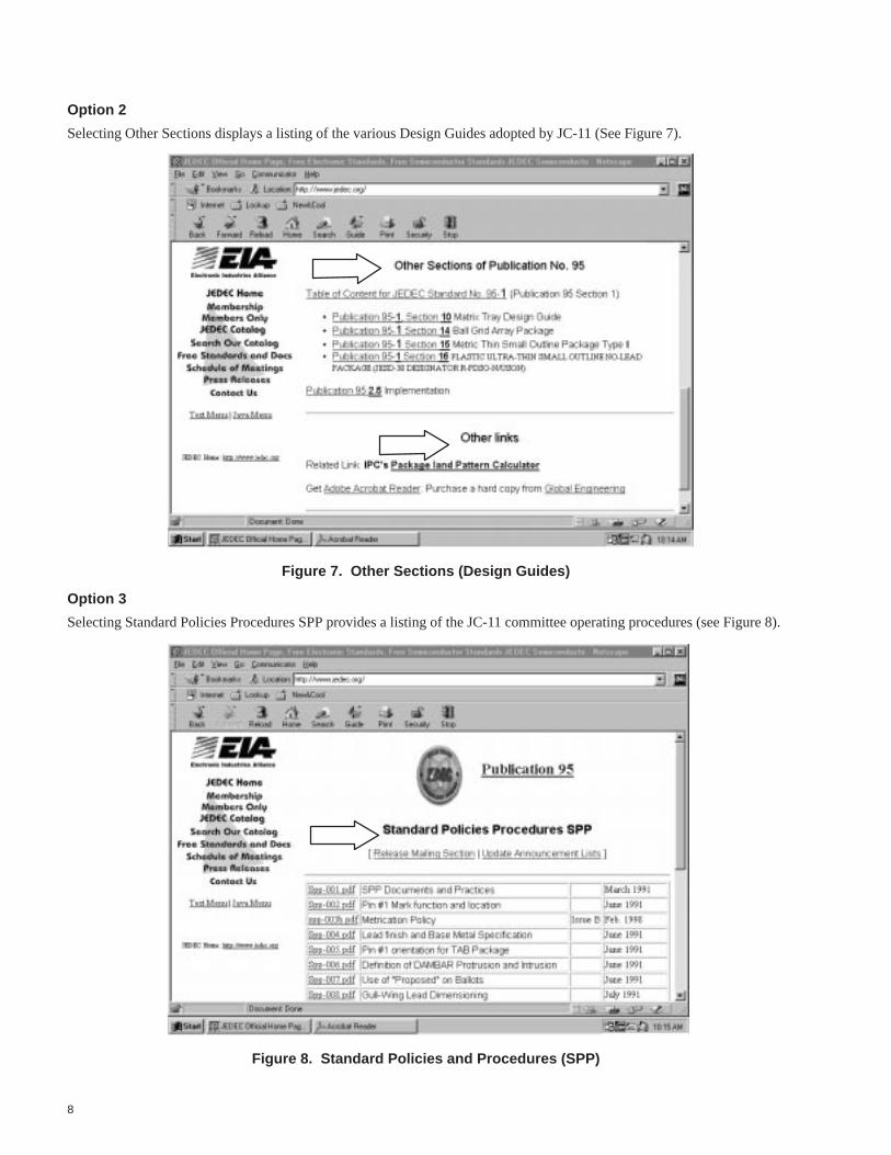
Option 2
Selecting Other Sections displays a listing of the various Design Guides adopted by JC-11 (See Figure 7).
Figure 7. Other Sections (Design Guides)
Option 3
Selecting Standard Policies Procedures SPP provides a listing of the JC-11 committee operating procedures (see Figure 8).
Figure 8. Standard Policies and Procedures (SPP)
9
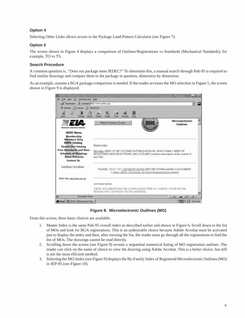
Option 4
Selecting Other Links allows access to the Package Land-Pattern Calculator (see Figure 7).
Option 5
The screen shown in Figure 4 displays a comparison of Outlines/Registrations vs Standards (Mechanical Standards); forexample, TO vs TS.
Search Procedure
A common question is, ‘‘Does our package meet JEDEC?” To determine this, a manual search through Pub-95 is required tofind similar drawings and compare them to the package in question, dimension by dimension.
As an example, assume a BGA package comparison is needed. If the reader accesses the MO selection in Figure 5, the screenshown in Figure 9 is displayed.
Figure 9. Microelectronic Outlines (MO)
From this screen, three basic choices are available.
1. Master Index is the same Pub-95 overall index as described earlier and shown in Figure 6. Scroll down to the listof MOs and look for BGA registrations. This is an undesirable choice because Adobe Acrobat must be activatedjust to display the index and then, after viewing the list, the reader must go through all the registrations to find thelist of MOs. The drawings cannot be read directly.
2. Scrolling down the screen (see Figure 9) reveals a sequential numerical listing of MO registration outlines. Thereader can click on the name of choice to view the drawing using Adobe Acrobat. This is a better choice, but stillis not the most efficient method.
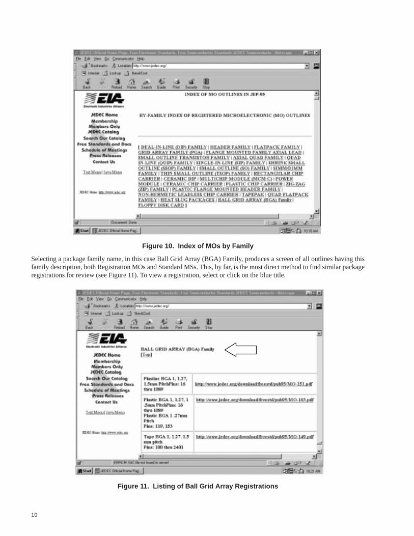
3. Selecting the MO-Index (see Figure 9) displays the By-Family Index of Registered Microelectronic Outlines (MO)in JEP-95 (see Figure 10).
10
Figure 10. Index of MOs by Family
Selecting a package family name, in this case Ball Grid Array (BGA) Family, produces a screen of all outlines having thisfamily description, both Registration MOs and Standard MSs. This, by far, is the most direct method to find similar packageregistrations for review (see Figure 11). To view a registration, select or click on the blue title.
Figure 11. Listing of Ball Grid Array Registrations
11
In the future, search acronyms such as SSOP, QFP, and PDIP will be added to the web page. By knowing the type package,the reader can search quickly for a particular package type and screen out many by the name description.
Guides for Designers
Various Design Guides are located on the Pub-95 web page (see Figure 5). There also is a link to the IPC Package Land-PatternCalculator.
Current Design Guides included in Pub 95-1 are:
Section 4: Quad FlatpackSection 10: Generic Matrix Tray for Handling and ShippingSection 11: Dual Inline Plastic FamilySection 13: Metric SOJ PackageSection 14: Ball Grid Array PackageSection 16: Fine-Pitch BGA (pending)
Summary
Pub-95 has been provided to member companies of JC-11 for many years. Access has been limited to committee members,alternates, or member companies willing to pay an added fee for additional copies. In the past, member-company employeeshad to contact the committee member to obtain information concerning package registration or registration details.
Today, anyone with web access can view a Registration or Standard and print a copy. The single most misunderstood factorwith JC-11 is the difference in Registrations and Standards. This difference has been explained, and readers can now understandthe difference and know how to find them efficiently by using the JEDEC web page.
12
Glossary
ASME American Society of Mechanical Engineers
ASME Y14.5M-1994 Dimensioning and Tolerancing Standard endorsed by JC-11
BGA Ball grid array package
EIA Electronic Industries Alliance (formerly known as Electronic Industries Association)
EIAJ Electronic Industries Association of Japan
GD&T Geometric Dimensioning & Tolerancing drafting methodology endorsed by ASME Y14.5M-1994and JC-11
IEC International Electrotechnical Commission
JC-11 Committee Number 11 of JEDEC, with responsibility for establishing package-outlineRegistrations and Standards
JEB-xx JEDEC Bulletin number xx
JEDEC Joint Electron Device Engineering Council
JEDEC BOD JEDEC Board of Directors (formerly known as the JEDEC Council)
JEDEC Standard 95-1 Section 4 of Pub-95, Design Guidelines
JEP-95 JEDEC Publication No. 95
Pub-95 Publication 95 of the JEDEC JC-11 committee
Registered Package-outline drawing approved by the JC-11 committee
SOJ Small-outline J-lead package
SPP Standard Policies and Procedures of the JC-11 committee
Standard JC-11 Registration that has attained wide use by the industry and now is recognized as anindustry standard
TSSOP Thin Shrink Small-Outline Package
13
Acknowledgment
John W. Yantis, P.E., is acknowledged as the author of this report. Sadly, John died in an accident prior to its publication.
John was a key contributor to TI’s Logic Products packaging group for over 25 years and was a TI representative to the JEDECJC-11 committee for packaging standardization. He was a key contributor to the JEDEC 95 Publication that this applicationreport describes and also chaired the JC-11.10 subcommittee on Microelectronic Ceramic Packages and the JC-11.7subcommittee on IEC Interface.
On behalf of John’s family, friends, and colleagues, we acknowledge his extensive contributions in his practice of engineeringand our pride in our association with him.
Bibliography
1. Publication No. 95, Registered Outlines for Solid State and Related Products, EIA, Arlington, VA, 1996.2. ASME Y14.5M-1994, Dimensioning and Tolerancing, The American Society of Mechanical Engineers, New York,
N.Y., 1995.3. http://www.jedec.org, EIA-JEDEC, Arlington, VA, 1997
14
Appendix A
Figure A–1. Example of a Registered-Outline Drawing Top Sheet
15
Figure A–2. Example of a Standard-Outline Drawing Top Sheet
16
Figure A–3. Example of a Carrier Registered-Outline Drawing Top Sheet
17
Figure A–4. Example of a Diode Registered-Outline (DO) Drawing Top Sheet