ITX-i290Dmedia.hpsindustrial.eftwee.nl/Manuals/Arbor/ITX-i290D.pdf · - II - Index LVDS-COMN1: LVDS...
61
ITX-i290D Mini ITX Industrial Motherboard User’s Manual Version 1.0 Copyright ® 2011 All Rights Reserved. 2011.08
Transcript of ITX-i290Dmedia.hpsindustrial.eftwee.nl/Manuals/Arbor/ITX-i290D.pdf · - II - Index LVDS-COMN1: LVDS...
ITX-i290DMini ITX Industrial Motherboard
User’s ManualVersion 1.0
Copyright® 2011 All Rights Reserved. 2011.08

This page is intentionally left blank.
- I -
Index
Table of ContentsChapter 1 - Introduction ...............................................................................1
1.1 Copyright Notice .........................................................................21.2 Declaration of Conformity ..........................................................21.3 About This User’s Manual ..........................................................31.4 Warning ........................................................................................31.5 Replacing the Lithium Battery ...................................................41.6 Technical Support .......................................................................41.7 Warranty .......................................................................................41.8 Packing List .................................................................................61.9 Ordering Information ..................................................................61.10 Specifications ............................................................................71.11 Rear Panel ..................................................................................81.12 MainBoard Layout .....................................................................8
Chapter 2 - Installation .................................................................................92.1 Block Diagram ...........................................................................102.2 CPU .............................................................................................102.3 FAN HEADER .............................................................................10
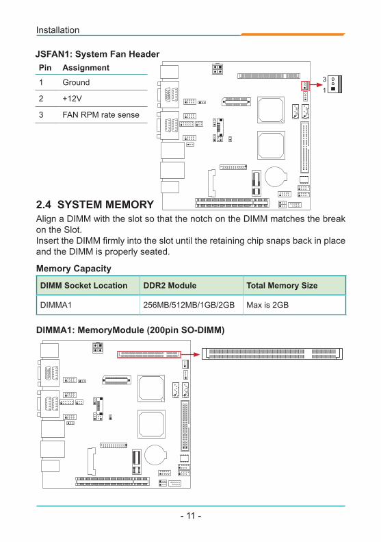
JSFAN1: System Fan Header ............................................................112.4 SYSTEM MEMORY..................................................................... 11
DIMMA1: MemoryModule (200pin SO-DIMM) ..................................112.5 POWER SUPPLY ........................................................................12
JATXPWR1: ATX Power Source Connector.....................................12JHDD1: SATA Power Connector .......................................................12
2.6 ONBOARD SLOT/CONNECTOR/HEADER/JUMPER ...............13PCI1: Peripheral Component Interconnect Slot ..............................13PE1: Mini PCI-E Slot ..........................................................................13IDE1: ATA Device Connector ............................................................14SATA1/SATA2: Serial ATA Connectors .............................................14JPANEL1: Front Panel Header ..........................................................15USB1/USB2: USB 2.0 Headers ..........................................................15JCOM1 / JCOM2 / JCOM3: Serial Port Connectors ........................16JSEL1/JSEL2: RS-232/422/485 Switch Headers (Optional) ............17JP2: Voltage Switch Header for JCOM2...........................................17JP3: Voltage Switch Header for JCOM3...........................................18JCOM4 ~ JCOM6: Serial Port Connectors .......................................18JDIO1: Digital I/O Connector ............................................................19JCMOS1: Clear CMOS Header * .......................................................19JAT1: AT/ATX Power Switch Header * ..............................................20JPRNT1: Printer Port Connector ......................................................20
- II -
Index
LVDS-COMN1: LVDS Connector .......................................................21JLV2: LCD Power Select Header * ....................................................22JBL1: LCD Backlight Power ON/OFF Header * ...............................23JBL2: LCD Backlight Brightness Adjust Header * ..........................23JC1: LCD Backlight Inverter Connector ..........................................23
2.7 The Installation Paths of CD Driver .........................................24Chapter 3 - BIOS .........................................................................................25
3.1 BIOS Introduction ......................................................................263.2 MAIN MENU................................................................................27
3.2.1 IDE Configuration ....................................................................283.3 ADVANCED MENU .....................................................................31
3.3.1 CPU Configuration ...................................................................313.3.2 SuperIO Configuration ............................................................323.3.3 Hardware Health Configuration ..............................................353.3.4 ACPI Configuration ..................................................................363.3.5 USB Configuration ...................................................................39
3.4 PCI/PNP MENU ..........................................................................413.4.1 PCI Resource ...........................................................................42
3.5 BOOT MENU ..............................................................................433.6 CHIPSET MENU .........................................................................45
3.6.1 North Bridge Configuration ....................................................453.6.2 South Bridge Configuration ....................................................48
3.7 EXIT MENU .................................................................................493.7.1 Security .....................................................................................50
Appendix - Useful Help ..............................................................................53Appendix A: AMI BIOS BEEP CODE ...............................................54
Boot Block Beep codes .....................................................................54POST BIOS Beep codes ....................................................................54Troubleshooting POST BIOS Beep codes .......................................55
Appendix B: TROUBLESHOOTING .................................................56

Introduction
- 1 -
1Chapter 1
Introduction
Chapter 1 - Introduction

Introduction
- 2 -
1.1 Copyright NoticeAll Rights Reserved.
The information in this document is subject to change without prior notice in order to improve the reliability, design and function. It does not represent a commitment on the part of the manufacturer.
Under no circumstances will the manufacturer be liable for any direct, indirect, special, incidental, or consequential damages arising from the use or inability to use the product or documentation, even if advised of the possibility of such damages.
This document contains proprietary information protected by copyright. All rights are reserved. No part of this manual may be reproduced by any mechanical, electronic, or other means in any form without prior written permission of the manufacturer.
1.2 Declaration of ConformityCEThis product has passed the CE test for environmental specifications when shielded cables are used for external wiring. This kind of cable is available from ARBOR. Please contact your local supplier for ordering information. Test conditions for passing included the equipment being operated within an industrial enclosure. In order to protect the product from being damaged by ESD (Electrostatic Discharge) and EMI leakage, we strongly recommend the use of CE-compliant industrial enclosure products.FCC Class BThis device complies with part 15 of the FCC Rules. Operation is subject to the following two conditions: (1) This device may not cause harmful interfer-ence, and (2) this device must accept any interference received, including interference that may cause undesired operation.This equipment has been tested and found to comply with the limits for a Class B digital device, pursuant to part 15 of the FCC Rules. These limits are designed to provide reasonable protection against harmful interference when the equipment is operated in a residential environment. This equipment generates, uses, and can radiate radio frequency energy and, if not installed and used in accordance with the instructions, may cause harmful interference to radio communications. Operation of this equipment in a residential area is likely to cause harmful interference in which case the user will be required to correct the interference at his own expense.

Introduction
- 3 -
RoHSARBOR Technology Corp. certifies that all components in its products are in compliance and conform to the European Union’s Restriction of Use of Haz-ardous Substances in Electrical and Electronic Equipment (RoHS) Directive 2002/95/EC.
The above mentioned directive was published on 2/13/2003. The main pur-pose of the directive is to prohibit the use of lead, mercury, cadmium, hexava-lent chromium, polybrominated biphenyls (PBB), and polybrominated diphenyl ethers (PBDE) in electrical and electronic products. Member states of the EU are to enforce by 7/1/2006.
ARBOR Technology Corp. hereby states that the listed products do not contain unintentional additions of lead, mercury, hex chrome, PBB or PBDB that ex-ceed a maximum concentration value of 0.1% by weight or for cadmium exceed 0.01% by weight, per homogenous material. Homogenous material is defined as a substance or mixture of substances with uniform composition (such as sol-ders, resins, plating, etc.). Lead-free solder is used for all terminations (Sn(96-96.5%), Ag(3.0-3.5%) and Cu(0.5%)).
SVHC / REACHTo minimize the environmental impact and take more responsibility to the earth we live, Arbor hereby confirms all products comply with the restriction of SVHC (Substances of Very High Concern) in (EC) 1907/2006 (REACH --Registration, Evaluation, Authorization, and Restriction of Chemicals) regulated by the European Union.
All substances listed in SVHC < 0.1 % by weight (1000 ppm)
1.3 About This User’s ManualThis user’s manual provides general information and installation instructions about the product. This User’s Manual is intended for experienced users and integrators with hardware knowledge of personal computers. If you are not sure about any description in this booklet. please consult your vendor before further handling.
1.4 WarningSingle Board Computers and their components contain very delicate Integrated Circuits (IC). To protect the Single Board Computer and its components against damage from static electricity, you should always follow the following precautions when handling it :

Introduction
- 4 -
1.5 Replacing the Lithium BatteryIncorrect replacement of the lithium battery may lead to a risk of explosion.
The lithium battery must be replaced with an identical battery or a battery type recommended by the manufacturer.
Do not throw lithium batteries into the trash-can. It must be disposed of in accordance with local regulations concerning special waste.
1.6 Technical SupportIf you have any technical difficulties, please do not hesitate to call or e-mail our customer service.
http://www.arbor.com.tw
E-mail:[email protected]
1.7 WarrantyThis product is warranted to be in good working order for a period of two years from the date of purchase. Should this product fail to be in good working order at any time during this period, we will, at our option, replace or repair it at no additional charge except as set forth in the following terms. This warranty does not apply to products damaged by misuse, modifications, accident or disaster.
Vendor assumes no liability for any damages, lost profits, lost savings or any other incidental or consequential damage resulting from the use, misuse of, or inability to use this product. Vendor will not be liable for any claim made by any other related party.
1. Disconnect your Single Board Computer from the power source when you want to work on the inside.
2. Hold the board by the edges and try not to touch the IC chips, leads or cir-cuitry.
3. Use a grounded wrist strap when handling computer components.
4. Place components on a grounded antistatic pad or on the bag that comes with the Single Board Computer, whenever components are separated from the system.
Introduction
- 5 -
Vendors disclaim all other warranties, either expressed or implied, including but not limited to implied warranties of merchantability and fitness for a particular purpose, with respect to the hardware, the accompanying product’s manual(s) and written materials, and any accompanying hardware. This limited warranty gives you specific legal rights.
Return authorization must be obtained from the vendor before returned merchandise will be accepted. Authorization can be obtained by calling or faxing the vendor and requesting a Return Merchandise Authorization (RMA) number. Returned goods should always be accompanied by a clear problem description.
Introduction
- 6 -
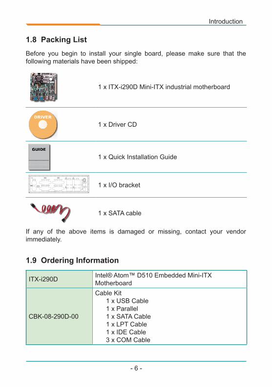
1.8 Packing ListBefore you begin to install your single board, please make sure that the following materials have been shipped:
1 x ITX-i290D Mini-ITX industrial motherboard
1 x Driver CD
1 x Quick Installation Guide
1 x I/O bracket
1 x SATA cable
If any of the above items is damaged or missing, contact your vendor immediately.
1.9 Ordering Information
ITX-i290D Intel® Atom™ D510 Embedded Mini-ITX Motherboard
CBK-08-290D-00
Cable Kit 1 x USB Cable 1 x Parallel 1 x SATA Cable 1 x LPT Cable 1 x IDE Cable 3 x COM Cable
Introduction
- 7 -
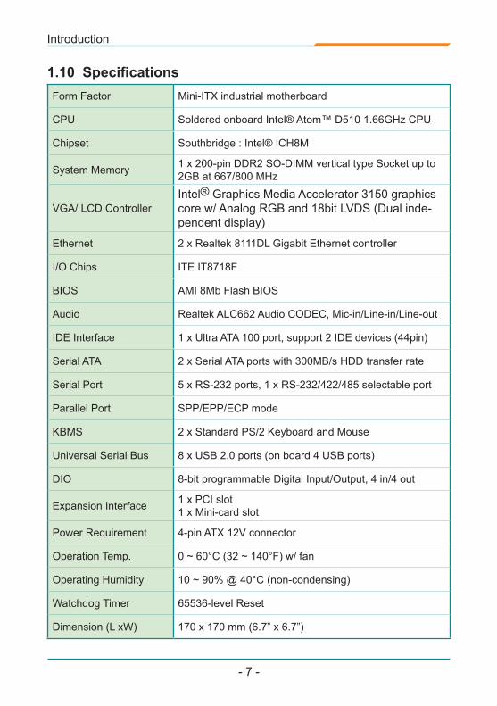
1.10 SpecificationsForm Factor Mini-ITX industrial motherboard
CPU Soldered onboard Intel® Atom™ D510 1.66GHz CPU
Chipset Southbridge : Intel® ICH8M
System Memory 1 x 200-pin DDR2 SO-DIMM vertical type Socket up to 2GB at 667/800 MHz
VGA/ LCD ControllerIntel® Graphics Media Accelerator 3150 graphics core w/ Analog RGB and 18bit LVDS (Dual inde-pendent display)
Ethernet 2 x Realtek 8111DL Gigabit Ethernet controller
I/O Chips ITE IT8718F
BIOS AMI 8Mb Flash BIOS
Audio Realtek ALC662 Audio CODEC, Mic-in/Line-in/Line-out
IDE Interface 1 x Ultra ATA 100 port, support 2 IDE devices (44pin)
Serial ATA 2 x Serial ATA ports with 300MB/s HDD transfer rate
Serial Port 5 x RS-232 ports, 1 x RS-232/422/485 selectable port
Parallel Port SPP/EPP/ECP mode
KBMS 2 x Standard PS/2 Keyboard and Mouse
Universal Serial Bus 8 x USB 2.0 ports (on board 4 USB ports)
DIO 8-bit programmable Digital Input/Output, 4 in/4 out
Expansion Interface 1 x PCI slot1 x Mini-card slot
Power Requirement 4-pin ATX 12V connector
Operation Temp. 0 ~ 60°C (32 ~ 140°F) w/ fan
Operating Humidity 10 ~ 90% @ 40°C (non-condensing)
Watchdog Timer 65536-level Reset
Dimension (L xW) 170 x 170 mm (6.7” x 6.7”)
Introduction
- 8 -
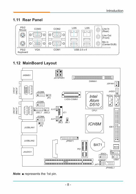
1.11 Rear Panel
1.12 MainBoard Layout
COM3
VGA
COM2 LAN LAN Line In(Rear)
Line Out(Front)
COM1 USB 2.0 x 4
Mic in(Center/SUB)
PS/2Mouse
PS/2Keyboard
JVG
A1
JCO
M3
JCO
M1
JCO
M2
JKBMS1
JUSBLAN1
JUSBLAN2
JAUDIO1
ICH8M
IntelAtomD510
JPRNT1
PE1
PCI1JAT1
JPANEL1
JCMOS1
JDIO1
USB1
US
B2
IDE1
SATA1 SATA2
JHDD1
JSFAN1
CPU1
DIMMA1JATXPWR1
JP3LVDS-COMN1
JCOM5
JCOM4
JCOM6
JSEL1 JSEL2JLV2
JLV1
JC1
JBL2 JBL1JP2
BAT1BIOS
PCI1
Note: ■ represents the 1st pin.
Installation
- 9 -
2Chapter 2
Installation
Chapter 2 - Installation
Installation
- 10 -
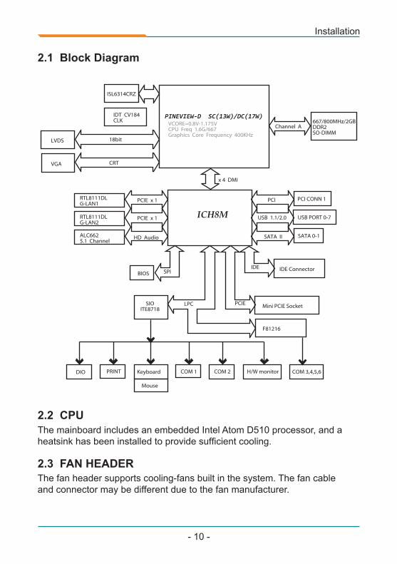
2.1 Block Diagram
ISL6314CRZ
VCORE=0.8V-1.175VCPU Freq 1.6G/667Graphics Core Frequency 400KHz
PINEVIEW-D SC(13W)/DC(17W)IDT CV184CLK
ICH8M
18bit
CRT
LVDS
VGA
RTL8111DLG-LAN1
PCIE x 1
PCIE x 1
HD Audio
BIOSIDE
PCI
x 4 DMI
PCI CONN 1
USB 1.1/2.0
SATA II
667/800MHz/2GBDDR2SO-DIMM
Channel A
USB PORT 0-7
SATA 0-1
PCIE
F81216
Mini PCIE Socket
IDE ConnectorSPI
LPCSIOITE8718
DIO PRINT Keyboard
Mouse
COM 1 COM 2 H/W monitor COM 3,4,5,6
RTL8111DLG-LAN2
ALC6625.1 Channel
2.2 CPU
2.3 FAN HEADER
The mainboard includes an embedded Intel Atom D510 processor, and aheatsink has been installed to provide sufficient cooling.
The fan header supports cooling-fans built in the system. The fan cableand connector may be different due to the fan manufacturer.
Installation
- 11 -
2.4 SYSTEM MEMORYAlign a DIMM with the slot so that the notch on the DIMM matches the break on the Slot.Insert the DIMM firmly into the slot until the retaining chip snaps back in place and the DIMM is properly seated.
JSFAN1: System Fan HeaderPin Assignment
1 Ground
2 +12V
3 FAN RPM rate sense
PCI1
31
DIMM Socket Location DDR2 Module Total Memory Size
DIMMA1 256MB/512MB/1GB/2GB Max is 2GB
Memory Capacity
PCI1
DIMMA1: MemoryModule (200pin SO-DIMM)
Installation
- 12 -
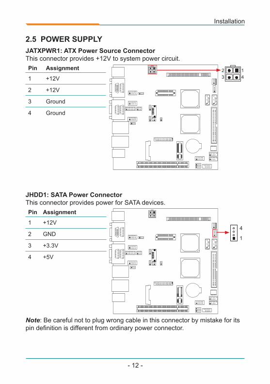
2.5 POWER SUPPLYJATXPWR1: ATX Power Source ConnectorThis connector provides +12V to system power circuit.Pin Assignment
1 +12V
2 +12V
3 Ground
4 Ground
JHDD1: SATA Power ConnectorThis connector provides power for SATA devices.Pin Assignment
1 +12V
2 GND
3 +3.3V
4 +5V
PCI1
PCI1
14
23
4
1
Note: Be careful not to plug wrong cable in this connector by mistake for its pin definition is different from ordinary power connector.
Installation
- 13 -
2.6 ONBOARD SLOT/CONNECTOR/HEADER/JUMPER
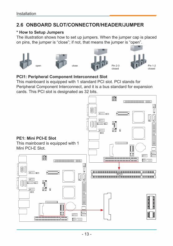
PCI1: Peripheral Component Interconnect SlotThis mainboard is equipped with 1 standard PCI slot. PCI stands for Peripheral Component Interconnect, and it is a bus standard for expansion cards. This PCI slot is designated as 32 bits.
PCI1
PCI1
* How to Setup JumpersThe illustration shows how to set up jumpers. When the jumper cap is placed on pins, the jumper is “close”; if not, that means the jumper is “open”.
open close Pin 2-3 closed
Pin 1-2 closed
PE1: Mini PCI-E SlotThis mainboard is equipped with 1 Mini PCI-E Slot.
PCI1
Installation
- 14 -
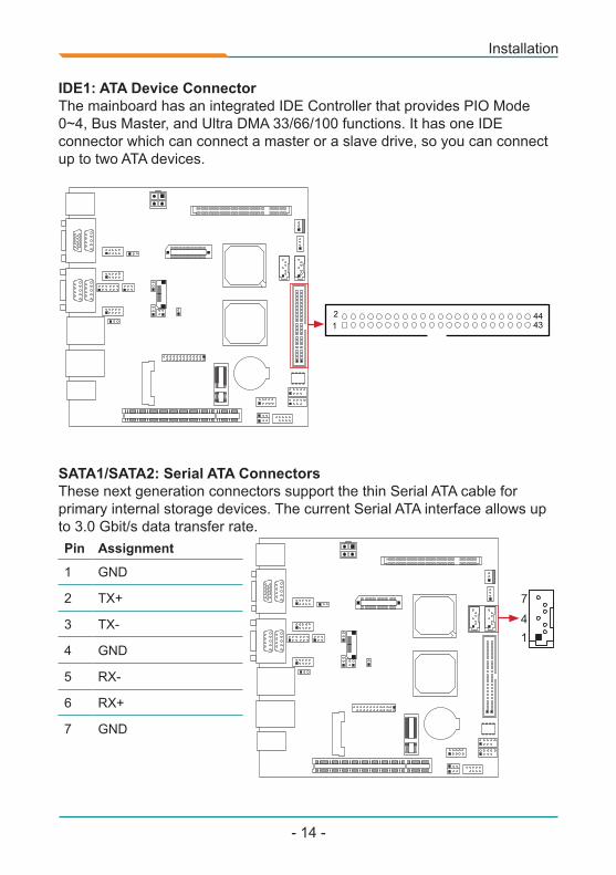
IDE1: ATA Device ConnectorThe mainboard has an integrated IDE Controller that provides PIO Mode0~4, Bus Master, and Ultra DMA 33/66/100 functions. It has one IDEconnector which can connect a master or a slave drive, so you can connect up to two ATA devices.
SATA1/SATA2: Serial ATA ConnectorsThese next generation connectors support the thin Serial ATA cable for primary internal storage devices. The current Serial ATA interface allows up to 3.0 Gbit/s data transfer rate.Pin Assignment
1 GND
2 TX+
3 TX-
4 GND
5 RX-
6 RX+
7 GND
PCI1
PCI1
12
4344
4
7
1
Installation
- 15 -
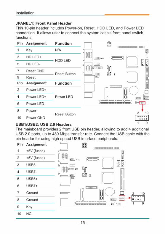
JPANEL1: Front Panel HeaderThis 10-pin header includes Power-on, Reset, HDD LED, and Power LEDconnection. It allows user to connect the system case’s front panel switchfunctions.Pin Assignment Function1 Key N/A
3 HD LED+HDD LED
5 HD LED-
7 Reset GNDReset Button
9 ResetPin Assignment Function2 Power LED+
Power LED4 Power LED+
6 Power LED-
8 PowerReset Button
10 Power GND
USB1/USB2: USB 2.0 HeadersThe mainboard provides 2 front USB pin header, allowing to add 4 additional USB 2.0 ports, up to 480 Mbps transfer rate. Connect the USB cable with the pin header for using high-speed USB interface peripherals.Pin Assignment
1 +5V (fused)
2 +5V (fused)
3 USB6-
4 USB7-
5 USB6+
6 USB7+
7 Ground
8 Ground
9 Key
10 NC
PCI1 1 9
2 10
PCI1
1 9
2 10
Installation
- 16 -
PCI1
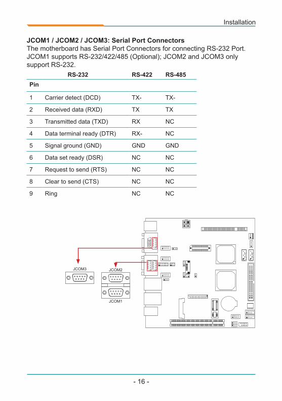
JCOM1 / JCOM2 / JCOM3: Serial Port ConnectorsThe motherboard has Serial Port Connectors for connecting RS-232 Port.JCOM1 supports RS-232/422/485 (Optional); JCOM2 and JCOM3 only support RS-232.
RS-232 RS-422 RS-485Pin
1 Carrier detect (DCD) TX- TX-
2 Received data (RXD) TX TX
3 Transmitted data (TXD) RX NC
4 Data terminal ready (DTR) RX- NC
5 Signal ground (GND) GND GND
6 Data set ready (DSR) NC NC
7 Request to send (RTS) NC NC
8 Clear to send (CTS) NC NC
9 Ring NC NC
JCOM3
JCOM2
JCOM1
JCOM3
JCOM2
JCOM1
Installation
- 17 -
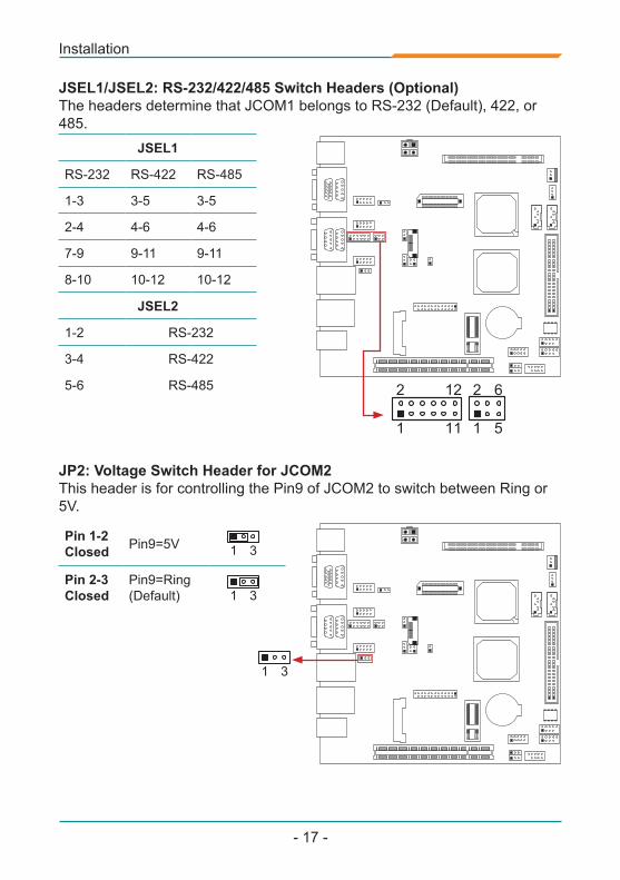
JSEL1/JSEL2: RS-232/422/485 Switch Headers (Optional)The headers determine that JCOM1 belongs to RS-232 (Default), 422, or 485.
JSEL1
RS-232 RS-422 RS-485
1-3 3-5 3-5
2-4 4-6 4-6
7-9 9-11 9-11
8-10 10-12 10-12
JSEL2
1-2 RS-232
3-4 RS-422
5-6 RS-485
PCI1
1 11 1 5
2 12 2 6
Pin 1-2 Closed Pin9=5V
1 3
1 3
1 3Pin 2-3 Closed
Pin9=Ring (Default)
1 3
1 3
1 3
JP2: Voltage Switch Header for JCOM2This header is for controlling the Pin9 of JCOM2 to switch between Ring or 5V.
PCI1
1 3
1 3
1 3

Installation
- 18 -
Pin 1-2 Closed Pin9=5V
1 3
1 3
1 3Pin 2-3 Closed
Pin9=Ring (Default)
1 3
1 3
1 3
JP3: Voltage Switch Header for JCOM3This header is for controlling the Pin9 of JCOM3 to switch between Ring or 5V.
PCI1
1 3
1 3
1 3
JCOM4 ~ JCOM6: Serial Port ConnectorsThe motherboard has 3 Serial Port Connectors for connecting RS-232 Port.Pin Assignment
1 -PDCD
2 PSIN
3 PSOUT data
4 -PDTR
5 GND
6 -PDSR
7 -PRTS
8 -PCTS
9 -PRI
10 5V (JCOM4/5) 12V (JCOM6)
PCI1
1 9
2 10
Installation
- 19 -
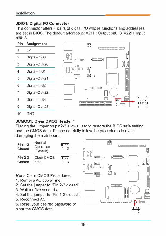
JDIO1: Digital I/O ConnectorThis connector offers 4 pairs of digital I/O whose functions and addresses are set in BIOS. The default address is: A21H: Output bit0~3; A22H: Input bit0~3.Pin Assignment
1 5V
2 Digital-In-30
3 Digital-Out-20
4 Digital-In-31
5 Digital-Out-21
6 Digital-In-32
7 Digital-Out-22
8 Digital-In-33
9 Digital-Out-23
10 GND
PCI1
1 9
2 10
Pin 1-2 Closed
Normal Operation (Default)
1 3
1 3
1 3Pin 2-3 Closed
Clear CMOS data
1 3
1 3
1 3
JCMOS1: Clear CMOS Header *Placing the jumper on pin2-3 allows user to restore the BIOS safe setting and the CMOS data. Please carefully follow the procedures to avoid damaging the mainboard.
Note: Clear CMOS Procedures1. Remove AC power line.2. Set the jumper to “Pin 2-3 closed”.3. Wait for five seconds.4. Set the jumper to “Pin 1-2 closed”.5. Reconnect AC.6. Reset your desired password or clear the CMOS data.
PCI1
1 3
1 3
1 3
Installation
- 20 -
Pin 1-2 Closed
For AT Power
1 3
1 3
1 3Pin 2-3 Closed
For ATX Power (De-fault)
1 3
1 3
1 3
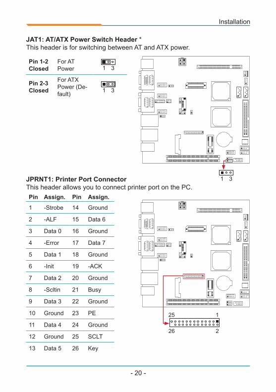
JAT1: AT/ATX Power Switch Header *This header is for switching between AT and ATX power.
1 3
1 3
1 3
PCI1
JPRNT1: Printer Port ConnectorThis header allows you to connect printer port on the PC.Pin Assign. Pin Assign.
1 -Strobe 14 Ground
2 -ALF 15 Data 6
3 Data 0 16 Ground
4 -Error 17 Data 7
5 Data 1 18 Ground
6 -Init 19 -ACK
7 Data 2 20 Ground
8 -Scltin 21 Busy
9 Data 3 22 Ground
10 Ground 23 PE
11 Data 4 24 Ground
12 Ground 25 SCLT
13 Data 5 26 Key
PCI1
125
226
Installation
- 21 -
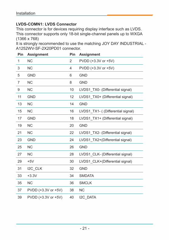
LVDS-COMN1: LVDS ConnectorThis connector is for devices requiring display interface such as LVDS.This connector supports only 18-bit single-channel panels up to WXGA (1366 x 768)It is strongly recommended to use the matching JOY DAY INDUSTRIAL -A1252WV-SF-2X20PD01 connector.Pin Assignment Pin Assignment
1 NC 2 PVDD (+3.3V or +5V)
3 NC 4 PVDD (+3.3V or +5V)
5 GND 6 GND
7 NC 8 GND
9 NC 10 LVDS1_TX0- (Differential signal)
11 GND 12 LVDS1_TX0+ (Differential signal)
13 NC 14 GND
15 NC 16 LVDS1_TX1- ( (Differential signal)
17 GND 18 LVDS1_TX1+ (Differential signal)
19 NC 20 GND
21 NC 22 LVDS1_TX2- (Differential signal)
23 GND 24 LVDS1_TX2+(Differential signal)
25 NC 26 GND
27 NC 28 LVDS1_CLK- (Differential signal)
29 +5V 30 LVDS1_CLK+(Differential signal)
31 I2C_CLK 32 GND
33 +3.3V 34 SMDATA
35 NC 36 SMCLK
37 PVDD (+3.3V or +5V) 38 NC
39 PVDD (+3.3V or +5V) 40 I2C_DATA
Installation
- 22 -
PCI1
1
2
39
40
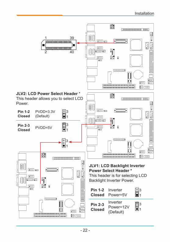
Pin 1-2 Closed
PVDD=3.3V (Default)
13
13
13
Pin 2-3 Closed PVDD=5V
13
13
13
Pin 1-2 Closed
Inverter Power=5V
13
13
13
Pin 2-3 Closed
Inverter Power=12V(Default)
13
13
13
JLV2: LCD Power Select Header *This header allows you to select LCD Power.
JLV1: LCD Backlight Inverter Power Select Header *This header is for selecting LCD Backlight Inverter Power.
13
13
13
PCI1
PCI1
Installation
- 23 -
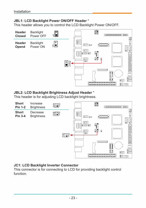
Header Closed
Backlight Power OFF
12
1
1Header Opend
Backlight Power ON
12
1
1
Short Pin 1-2
Increase Brightness
1234
1234
1234Short
Pin 3-4Decrease Brightness
1234
1234
1234
JBL1: LCD Backlight Power ON/OFF Header *This header allows you to control the LCD Backlight Power ON/OFF.
JBL2: LCD Backlight Brightness Adjust Header *This header is for adjusting LCD backlight brightness.
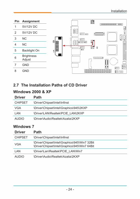
JC1: LCD Backlight Inverter ConnectorThis connector is for connecting to LCD for providing backlight control function.
12
1
1
1234
1234
1234
PCI1
PCI1
Installation
- 24 -
Pin Assignment
1 5V/12V DC
2 5V/12V DC
3 NC
4 NC
5 Backlight On
6 Brightness Adjust
7 GND
8 GND PCI1
1
8
2.7 The Installation Paths of CD DriverWindows 2000 & XP Driver PathCHIPSET \Driver\Chipset\Intel\Infinst
VGA \Driver\Chipset\Intel\Graphics\945\2KXP
LAN \Driver\LAN\Realtek\PCIE_LAN\2KXP
AUDIO \Driver\Audio\Realtek\Azalia\2KXP
Windows 7Driver PathCHIPSET \Driver\Chipset\Intel\Infinst
VGA \Driver\Chipset\Intel\Graphics\945\Win7 32Bit\Driver\Chipset\Intel\Graphics\945\Win7 64Bit
LAN \Driver\Lan\Realtek\PCIE_LAN\Win7
AUDIO \Driver\Audio\Realtek\Azalia\2KXP
BIOS
- 25 -
3Chapter 3
BIOS
Chapter 3 - BIOS

BIOS
- 26 -
The purpose of this chapter is to describe the settings in the AMI BIOSSetup program of this motherboard. The Setup program allows users tomodify the basic system configuration and save these settings to CMOS RAM.The power of CMOS RAM is supplied by a battery so that it retains theSetup information when the power is turned off.Basic Input-Output System (BIOS) determines what a computer can dowithout accessing programs from a disk. This system controls most of theinput and output devices such as keyboard, mouse, serial ports and diskdrives. BIOS activates at the first stage of the booting process, loading andexecuting the operating system. Some additional features, such as virus andpassword protection or chipset fine-tuning options are also included in BIOS.The rest of this manual will guide you through the options and settings inBIOS Setup.
This AMI BIOS supports the Plug and Play Version 1.0A.
This AMI BIOS supports Version 1.03 of the EPA Green PC.
DDR2 SDRAM (Double Data Rate II Synchronous DRAM) is supported.
This AMI BIOS supports the Intel CPU.
AMI ACPI BIOS support Version 1.0/2.0 of Advanced Configuration andPower interface (ACPI). It provides ASL code for powermanagement and device configuration capabilities as defined in the ACPI, developed by Microsoft, Intel and Toshiba.
This AMI BIOS also supports Version 2.3 of the Intel PCI (PeripheralComponent Interconnect) local bus.
3.1 BIOS Introduction
Plug and Play Support
EPA Green PC Support
DRAM Support
Supported CPUs
Using Setup
ACPI Support
PCI Bus Support
BIOS
- 27 -
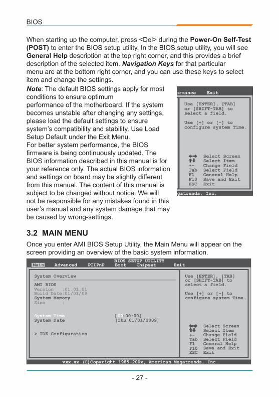
When starting up the computer, press <Del> during the Power-On Self-Test (POST) to enter the BIOS setup utility. In the BIOS setup utility, you will seeGeneral Help description at the top right corner, and this provides a briefdescription of the selected item. Navigation Keys for that particularmenu are at the bottom right corner, and you can use these keys to select item and change the settings.Note: The default BIOS settings apply for most conditions to ensure optimumperformance of the motherboard. If the system becomes unstable after changing any settings, please load the default settings to ensure system’s compatibility and stability. Use Load Setup Default under the Exit Menu.For better system performance, the BIOS firmware is being continuously updated. The BIOS information described in this manual is for your reference only. The actual BIOS information and settings on board may be slightly different from this manual. The content of this manual is subject to be changed without notice. We will not be responsible for any mistakes found in this user’s manual and any system damage that may be caused by wrong-settings.
Once you enter AMI BIOS Setup Utility, the Main Menu will appear on thescreen providing an overview of the basic system information.
3.2 MAIN MENU
BIOS SETUP UTILITYMain Advanced PCIPnP Boot Chipset
vxx.xx (C)Copyright 1985-200x, American Megatrends, Inc.
Select ScreenSelect ItemChange FieldSelect FieldGeneral HelpSave and ExitExit
+-TabF1F10ESC
Use [ENTER], [TAB] or [SHIFT-TAB] to select a field.
Use [+] or [-] toconfigure system Time.
System Overview
AMI BIOS
System Memory
[ :00:00]System Date [Thu 01/01/2009]
> IDE Configuration
Version :01.01.01Build Date:01/01/09
Size :
System Time 00
Exit
BIOS
- 28 -
Shows system memory size, VGA share memory will be excluded.
Set the system internal clock.
Set the system date. Note that the ‘Day’ automatically changes when youset the date.
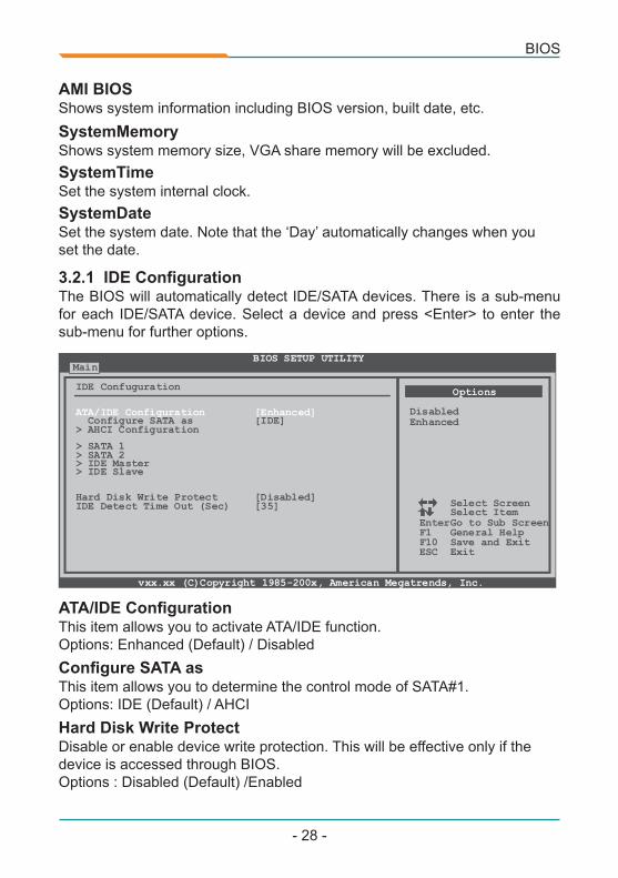
This item allows you to activate ATA/IDE function.Options: Enhanced (Default) / Disabled
The BIOS will automatically detect IDE/SATA devices. There is a sub-menu for each IDE/SATA device. Select a device and press <Enter> to enter the sub-menu for further options.
This item allows you to determine the control mode of SATA#1.Options: IDE (Default) / AHCI
Shows system information including BIOS version, built date, etc.SystemMemory
SystemTime
SystemDate
ATA/IDE Configuration
3.2.1 IDE Configuration
Configure SATA as
AMI BIOS
BIOS SETUP UTILITYMain
vxx.xx (C)Copyright 1985-200x, American Megatrends, Inc.
Select ScreenSelect ItemGo to Sub ScreenGeneral HelpSave and ExitExit
EnterF1F10ESC
IDE Confuguration
Configure SATA as [IDE]
> SATA 1> SATA 2> IDE Master> IDE Slave
Hard Disk Write Protect [Disabled]IDE Detect Time Out (Sec) [35]
> AHCI Configuration
ATA/IDE Configuration [Enhanced]
Options
DisabledEnhanced
Disable or enable device write protection. This will be effective only if thedevice is accessed through BIOS.Options : Disabled (Default) /Enabled
Hard Disk Write Protect
BIOS
- 29 -
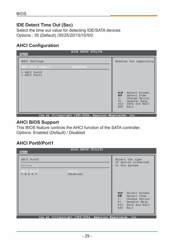
This BIOS feature controls the AHCI function of the SATA controller.Options: Enabled (Default) / Disabled
AHCI BIOS Support
AHCI Configuration
AHCI Port0/Port1
BIOS SETUP UTILITYMain
vxx.xx (C)Copyright 1985-200x, American Megatrends, Inc.
Select ScreenSelect ItemChange OptionGeneral HelpSave and ExitExit
+-F1F10ESC
AHCI Settings
> AHCI Port0> AHCI Port1
AHCI BIOS Support [Enabled]
Enables for supporting
BIOS SETUP UTILITYMain
vxx.xx (C)Copyright 1985-200x, American Megatrends, Inc.
Select ScreenSelect ItemChange OptionGeneral HelpSave and ExitExit
+-F1F10ESC
AHCI Port0
S.M.A.R.T. [Enabled]
Device :
AHCI Port0 [Auto]
Select the typeof device connectedto the system.
Select the time out value for detecting IDE/SATA devicesOptions : 35 (Default) /30/25/20/15/10/5/0
IDE Detect Time Out (Sec)
BIOS
- 30 -
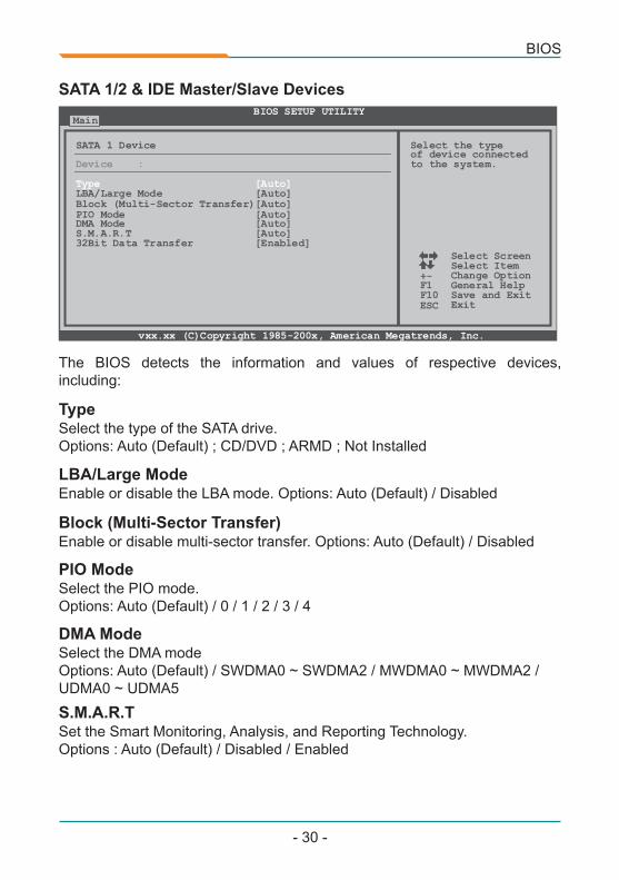
SATA 1/2 & IDE Master/Slave DevicesBIOS SETUP UTILITY
Main
vxx.xx (C)Copyright 1985-200x, American Megatrends, Inc.
Select ScreenSelect ItemChange OptionGeneral HelpSave and ExitExit
+-F1F10ESC
Select the typeof device connectedto the system.
SATA 1 Device
LBA/Large Mode [Auto]Block (Multi-Sector Transfer)[Auto]PIO Mode [Auto]DMA Mode [Auto]S.M.A.R.T [Auto]32Bit Data Transfer [Enabled]
Device :
Type [Auto]
Enable or disable the LBA mode. Options: Auto (Default) / Disabled
Enable or disable multi-sector transfer. Options: Auto (Default) / Disabled
Select the PIO mode.Options: Auto (Default) / 0 / 1 / 2 / 3 / 4
Set the Smart Monitoring, Analysis, and Reporting Technology.Options : Auto (Default) / Disabled / Enabled
Select the DMA modeOptions: Auto (Default) / SWDMA0 ~ SWDMA2 / MWDMA0 ~ MWDMA2 /UDMA0 ~ UDMA5
The BIOS detects the information and values of respective devices, including:
Select the type of the SATA drive.Options: Auto (Default) ; CD/DVD ; ARMD ; Not Installed
LBA/Large Mode
Block (Multi-Sector Transfer)
PIO Mode
S.M.A.R.T
DMA Mode
Type
BIOS
- 31 -
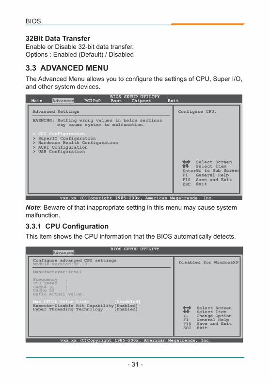
Enable or Disable 32-bit data transfer.Options : Enabled (Default) / Disabled
32Bit Data Transfer
The Advanced Menu allows you to configure the settings of CPU, Super I/O, and other system devices.
Note: Beware of that inappropriate setting in this menu may cause system malfunction.
3.3 ADVANCED MENU
BIOS SETUP UTILITYMain Advanced PCIPnP Boot Chipset
vxx.xx (C)Copyright 1985-200x, American Megatrends, Inc.
Select ScreenSelect ItemGo to Sub ScreenGeneral HelpSave and ExitExit
EnterF1F10ESC
Configure CPU.Advanced Settings
WARNING: Setting wrong values in below sections may cause system to malfunction.
> USB Configuration
> SuperIO Configuration> Hardware Health Configuration> ACPI Configuration
> CPU Configuration
Exit
3.3.1 CPU Configuration
BIOS SETUP UTILITYAdvanced
vxx.xx (C)Copyright 1985-200x, American Megatrends, Inc.
Select ScreenSelect ItemChange OptionGeneral HelpSave and ExitExit
+-F1F10ESC
Disabled for WindowsXPConfigure advanced CPU settingsModule Version:3F.19
Manufacturer:Intel
Frequency :FSB Speed :Cache L1 :Cache L2 :Ratio Actual Value:
Max CPUID Value Limit [Disabled]Execute-Disable Bit Capability[Enabled]Hyper Threading Technology [Enabled]
This item shows the CPU information that the BIOS automatically detects.
BIOS
- 32 -
When the computer boots up, the operating system will execute the CPUIDinstruction to identify the processor and its capabilities. Before it can do so, it must first query the processor to find out the highest input value CPUID recognized. This determines the kind of basic information CPUID can provide to the operating system.Options: Disabled (Default) / Enabled
Enabled for Windows XP and Linux (OS optimized for Hyper ThreadingTechnology) and disabled for other OS (OS not optimized for Hyper Threading Technology).Options: Enabled (Default) / Disabled
This item allows you to configure the Execute-Disabled Bit function, which protects your system from buffer overflow attacks.Options: Enabled (Default) / Disabled
Max CPUID Value Limit
Hyper Threading Technology
Execute-Disable Bit Capability
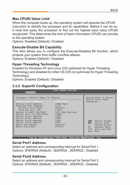
3.3.2 SuperIO ConfigurationBIOS SETUP UTILITY
Advanced
vxx.xx (C)Copyright 1985-200x, American Megatrends, Inc.
Select ScreenSelect ItemChange OptionGeneral HelpSave and ExitExit
+-F1F10ESC
Allows BIOS to SelectSerial Port1 BaseAddresses.
Configure ITE8718 Super IO Chipset
Serial Port1 Address [3F8/IRQ4]
Second IO UART IRQ MODE [PCI IRQ Sharing]
Serial Port2 Address [2F8/IRQ3]Parallel Port Address [378] Parallel Port Mode [Normal] Parallel Port IRQ [IRQ7]
Serial Port 3-6 IRQ Share [IRQ5]Serial Port3 Address [3E8]Serial Port4 Address [2E8]Serial Port5 Address [2F0]Serial Port6 Address [2E0]Watch Dog Degree [Second]Watch Dog Timer [00000]
Select an address and corresponding interrupt for Serial Port 2.Options: 2F8/IRQ3 (Default) ; 3E8/IRQ4 ; 2E8/IRQ3 ; Disabled
Select an address and corresponding interrupt for Serial Port 1.Options: 3F8/IRQ4 (Default) ; 3E8/IRQ4 ; 2E8/IRQ3 ; Disabled
Serial Port2 Address
Serial Port1 Address
BIOS
- 33 -
This item allows you to determine how the parallel port should function.Options: Normal (Default) Using Parallel port as Standard Printer Port. EPP Using Parallel Port as Enhanced Parallel Port. ECP Using Parallel port as Extended Capabilities Port. ECP+EPP Using Parallel port as ECP & EPP mode.
This item allows you to determine access onboard parallel port controller with which I/O Address.Options: 378 (Default) / 278 / 3BC / Disabled
This item allows you to select the IRQ for the onboard parallel port.Options: IRQ7 (Default) / IRQ5
This item allows you to select parallel port ECP DMA.Options: DMA3 (Default) / DMA0 / DMA1
Parallel Port Address
Parallel Port Mode
Parallel Port IRQ
ECP Mode DMA Channel
This item allows you to determine whether Serial Port 3-6 share IRQ.Options: IRQ5 (Default) / Disabled / IRQ3 / IRQ4 / IRQ7 / IRQ9 / IRQ10 / IRQ11 / IRQ12
This item allows you to select IRQ of Serial Port3.Options: IRQ5 (Default) / IRQ3 / IRQ4 / IRQ7 / IRQ9 / IRQ10 / IRQ11 / IRQ12
PCI IRQ Sharing for OS (EX. WinXP); ISA IRQ Sharing for Dos.Options: PCI IRQ Sharing (Default) / ISA IRQ
This item allows you to select the address of Serial Port3.Options: 3E8 (Default) / 2E8 / 2F0 / 2E0
Serial Port 3-6 IRQ Share
Serial Port3 IRQ
Second IO UART IRQ Mode
Serial Port3 Address
This item allows you to select the address of Serial Port4.Options: 2E8 (Default) / 3E8 / 2F0 / 2E0
Serial Port4 Address
BIOS
- 34 -
This item allows you to select IRQ of Serial Port5.Options: IRQ5 (Default) / IRQ3 / IRQ4 / IRQ7 / IRQ9 / IRQ10 / IRQ11 / IRQ12
This item allows you to select IRQ of Serial Port6.Options: IRQ5 (Default) / IRQ3 / IRQ4 / IRQ7 / IRQ9 / IRQ10 / IRQ11 / IRQ12
Options: 0 for disabled (Default) / Min=1, Max=65536
This item allows you to select the address of Serial Port5.Options: 2F0 (Default) / 3E8 / 2E8 / 2E0
This item allows you to select the address of Serial Port6.Options: 2E0 (Default) / 3E8 / 2E8 / 2F0
This item allows you to determine the functional degree of Watch Dog.Options: Second (Default) / Minute
Serial Port5 IRQ
Serial Port6 IRQ
Watch Dog Timer
Serial Port5 Address
Serial Port6 Address
Watch Dog Degree
This item allows you to select IRQ of Serial Port4.Options: IRQ5 (Default) / IRQ3 / IRQ4 / IRQ7 / IRQ9 / IRQ10 / IRQ11 / IRQ12
Serial Port4 IRQ
BIOS
- 35 -
This item allows you to set up the CPU shutdown temperature. This item is only effective under Windows 98 ACPI mode.Options: Disabled (Default) ; 60°C/140°F ; 65°C/149°F ; 70°C/158°F ; 5°C/167°F ; 80°C/176°F ; 85°C/185°F ; 90°C/194°F
With a monitoring system, it will show PC health status during POST stage.Options: Enabled (Default) / Disabled
Shutdown Temperature Function
H/W Health Function
3.3.3 Hardware Health Configuration
Advanced
Hardware Health Configuration
H/W Health Function [Enabled]Shutdown Temperature [Disabled]
CPU TemperatureSYSTEM Temperature
JSFan1 Speed
CPU VCoreSB Voltage+3.30V+5.00V+12.0VGMCH VCoreMemory Voltage5VSB
BIOS SETUP UTILITY
vxx.xx (C)Copyright 1985-200x, American Megatrends, Inc.
Select ScreenSelect ItemChange OptionGeneral HelpSave and ExitExit
+-F1F10ESC
Enables HardwareHealth MonitoringDevice.
This item shows the system temperature, fan speed, and voltage information.
BIOS
- 36 -
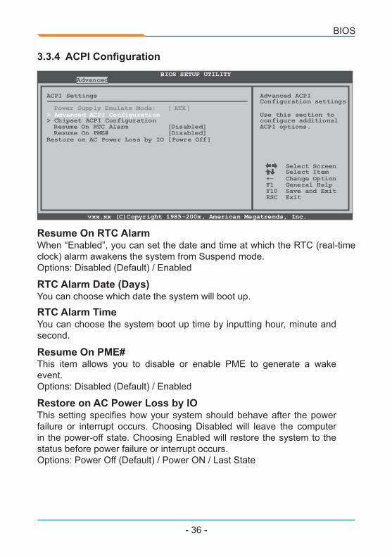
3.3.4 ACPI ConfigurationBIOS SETUP UTILITY
Advanced
vxx.xx (C)Copyright 1985-200x, American Megatrends, Inc.
Select ScreenSelect ItemChange OptionGeneral HelpSave and ExitExit
+-F1F10ESC
ACPI Settings
Power Supply Emulate Mode: [ ]ATX> Advanced ACPI Configuration> Chipset ACPI Configuration
Resume On PME# [Disabled]Restore on AC Power Loss by IO [Powre Off]
Resume On RTC Alarm [Disabled]
Advanced ACPIConfiguration settings
Use this section toconfigure additionalACPI options.
When “Enabled”, you can set the date and time at which the RTC (real-time clock) alarm awakens the system from Suspend mode.Options: Disabled (Default) / Enabled
You can choose the system boot up time by inputting hour, minute and second.
This item allows you to disable or enable PME to generate a wake event.Options: Disabled (Default) / Enabled
This setting specifies how your system should behave after the power failure or interrupt occurs. Choosing Disabled will leave the computer in the power-off state. Choosing Enabled will restore the system to the status before power failure or interrupt occurs.Options: Power Off (Default) / Power ON / Last State
You can choose which date the system will boot up.
Resume On RTC Alarm
RTC Alarm Time
Restore on AC Power Loss by IO
RTC Alarm Date (Days)
Resume On PME#

BIOS
- 37 -
The item allows you to select the version of ACPI.Options: ACPI v1.0 (Default) / ACPI v2.0 / ACPI v3.0
This item is used to enable or disable the motherboard's APIC (AdvancedProgrammable Interrupt Controller). The APIC provides multiprocessor support, more IRQs and faster interrupt handling.Options: Enabled (Default) / Disabled
Set this value to allow the ACPI BIOS to add a pointer to an OEMB table in the Root System Description Table (RSDT).Options: Enabled (Default) / Disabled
This is a server-specific feature. A headless server is one that operates without a keyboard, monitor or mouse. To run in headless mode, both BIOS and operating system (e.g. Windows Server 2003) must support headless operation.Options: Disabled (Default) / Enabled
Advanced ACPI Configuration
ACPI Version Features
ACPI APIC support
AMI OEMB table
Headless mode
BIOS SETUP UTILITYAdvanced
vxx.xx (C)Copyright 1985-200x, American Megatrends, Inc.
Select ScreenSelect ItemChange OptionGeneral HelpSave and ExitExit
+-F1F10ESC
Advanced ACPI Configuration
ACPI Version Features [ACPI v1.0]ACPI APIC support [Enabled]
Headless mode [Disabled]AMI OEMB table [Enabled]
Enable RSDP pointersto 64-bit Fixed SystemDescription Tables.ACPI version has some
BIOS
- 38 -
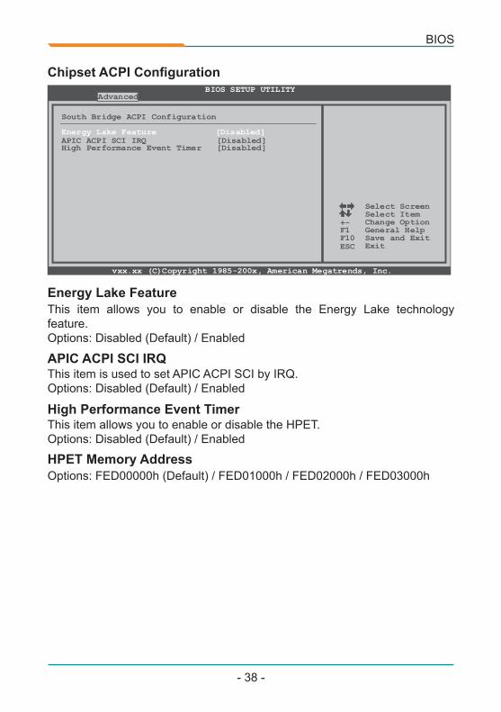
This item is used to set APIC ACPI SCI by IRQ.Options: Disabled (Default) / Enabled
Options: FED00000h (Default) / FED01000h / FED02000h / FED03000h
This item allows you to enable or disable the HPET.Options: Disabled (Default) / Enabled
APIC ACPI SCI IRQ
HPET Memory Address
High Performance Event Timer
Chipset ACPI ConfigurationBIOS SETUP UTILITY
Advanced
vxx.xx (C)Copyright 1985-200x, American Megatrends, Inc.
Select ScreenSelect ItemChange OptionGeneral HelpSave and ExitExit
+-F1F10ESC
South Bridge ACPI Configuration
Energy Lake Feature [Disabled]APIC ACPI SCI IRQ [Disabled]High Performance Event Timer [Disabled]
This item allows you to enable or disable the Energy Lake technology feature.Options: Disabled (Default) / Enabled
Energy Lake Feature
BIOS
- 39 -
This item allows you to select the operation mode of the USB 2.0 controller.Options: HiSpeed (Default) USB 2.0-480Mbps FullSpeed USB 1.1-12Mbps
This item allows you to activate USB1.1 HC support.Options: Enabled (Default) / Disabled
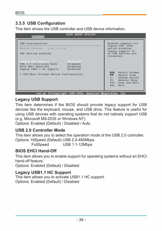
This item shows the USB controller and USB device information.
USB 2.0 Controller Mode
Legacy USB1.1 HC Support
This item determines if the BIOS should provide legacy support for USB devices like the keyboard, mouse, and USB drive. This feature is useful for using USB devices with operating systems that do not natively support USB (e.g. Microsoft MS-DOS or Windows NT).Options: Enabled (Default) / Disabled / Auto
This item allows you to enable support for operating systems without an EHCI hand-off feature.Options: Enabled (Default) / Disabled
Legacy USB Support
BIOS EHCI Hand-Off
3.3.5 USB Configuration
BIOS SETUP UTILITYAdvanced
vxx.xx (C)Copyright 1985-200x, American Megatrends, Inc.
Select ScreenSelect ItemChange OptionGeneral HelpSave and ExitExit
+-F1F10ESC
Enables support forlegacy USB. AUTOoption disables legacy support ifno USB devices areconnected.
USB Configuration
USB Devices Enabled:
Module Version - 2.24.5-13.4
Legacy USB Support [Enabled]USB 2.0 Controller Mode [HiSpeed]BIOS EHCI Hand-Off [Enabled]Legacy USB1.1 HC Support [Enabled]
> USB Mass Storage Device Configuration
BIOS
- 40 -
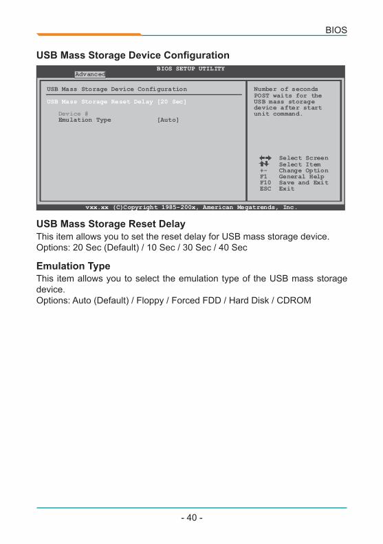
USB Mass Storage Device ConfigurationBIOS SETUP UTILITY
Advanced
vxx.xx (C)Copyright 1985-200x, American Megatrends, Inc.
Select ScreenSelect ItemChange OptionGeneral HelpSave and ExitExit
+-F1F10ESC
Number of secondsPOST waits for theUSB mass storagedevice after startunit command.
USB Mass Storage Device Configuration
USB Mass Storage Reset Delay [20 Sec]
Emulation Type [Auto]
Device #
This item allows you to select the emulation type of the USB mass storage device.Options: Auto (Default) / Floppy / Forced FDD / Hard Disk / CDROM
Emulation Type
This item allows you to set the reset delay for USB mass storage device.Options: 20 Sec (Default) / 10 Sec / 30 Sec / 40 Sec
USB Mass Storage Reset Delay
BIOS
- 41 -
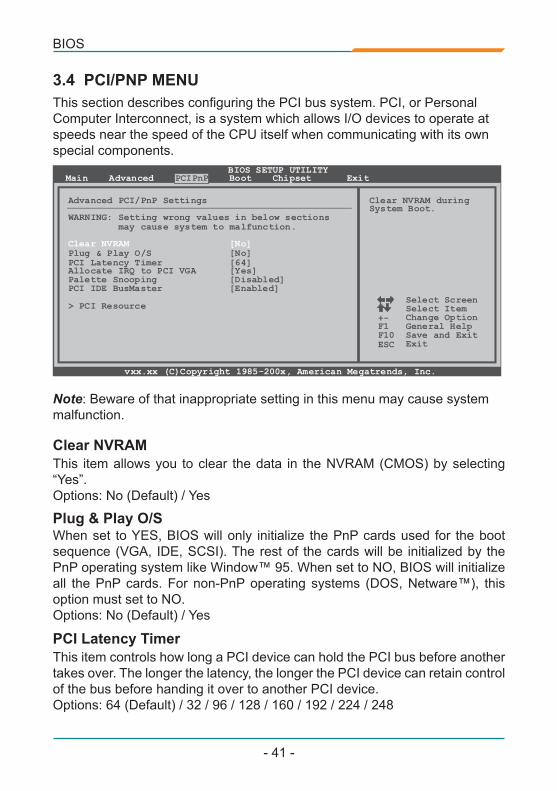
This section describes configuring the PCI bus system. PCI, or Personal Computer Interconnect, is a system which allows I/O devices to operate at speeds near the speed of the CPU itself when communicating with its own special components.
Note: Beware of that inappropriate setting in this menu may cause system malfunction.
3.4 PCI/PNP MENU
BIOS SETUP UTILITYMain Advanced PCIPnP Boot Chipset
vxx.xx (C)Copyright 1985-200x, American Megatrends, Inc.
Select ScreenSelect ItemChange OptionGeneral HelpSave and ExitExit
+-F1F10ESC
Clear NVRAM duringSystem Boot.
Advanced PCI/PnP Settings
WARNING: Setting wrong values in below sections may cause system to malfunction.
Plug & Play O/S [No]PCI Latency Timer [64]Allocate IRQ to PCI VGA [Yes]Palette Snooping [Disabled]PCI IDE BusMaster [Enabled]
> PCI Resource
Clear NVRAM [No]
Exit
When set to YES, BIOS will only initialize the PnP cards used for the boot sequence (VGA, IDE, SCSI). The rest of the cards will be initialized by the PnP operating system like Window™ 95. When set to NO, BIOS will initialize all the PnP cards. For non-PnP operating systems (DOS, Netware™), this option must set to NO.Options: No (Default) / Yes
This item controls how long a PCI device can hold the PCI bus before another takes over. The longer the latency, the longer the PCI device can retain control of the bus before handing it over to another PCI device.Options: 64 (Default) / 32 / 96 / 128 / 160 / 192 / 224 / 248
Plug & Play O/S
PCI Latency Timer
This item allows you to clear the data in the NVRAM (CMOS) by selecting “Yes”.Options: No (Default) / Yes
Clear NVRAM
BIOS
- 42 -
This item is a toggle for the built-in driver that allows the onboard IDE controller to perform DMA (Direct Memory Access) transfers.Options: Enabled (Default) / Disabled
Some old graphic controllers need to “snoop” on the VGA palette and then map it to their display as a way to provide boot information and VGA compatibility. This item allows such snooping to take place.Options: Disabled (Default) / Enabled
PCI IDE BusMaster
Palette Snooping
This item allows BIOS to choose a IRQ to assign for the PCI VGA card.Options: Yes (Default) / No
These items will allow you to assign each system interrupt a type, depending on the type of device using the interrupt. The option “Available” means the IRQ is going to assign automatically.Options: Available (Default) / Reserved
Allocate IRQ to PCI VGA
IRQ3/4/5/7/9/10/11/14/15
3.4.1 PCI ResourceBIOS SETUP UTILITY
PCIPnP
vxx.xx (C)Copyright 1985-200x, American Megatrends, Inc.
Select ScreenSelect ItemChange OptionGeneral HelpSave and ExitExit
+-F1F10ESC
Available: SpecifiedIRQ is available to beused by PCI/PnPdevices.Reserved: SpecifiedIRQ is reserved foruse by Legacy ISAdevices.
PCI Resource
IRQ3 [Available]IRQ4 [Available]IRQ5 [Available]IRQ7 [Available]IRQ9 [Available]IRQ10 [Available]IRQ11 [Available]IRQ14 [Available]IRQ15 [Available]
DMA Channel 0 [Available]DMA Channel 1 [Available]DMA Channel 3 [Available]DMA Channel 5 [Available]DMA Channel 6 [Available]DMA Channel 7 [Available]
Reserved Memory Size [Disabled]
BIOS
- 43 -
This item allows BIOS to reserve certain memory size for specific PCI device.Options: Disabled (Default) / 16K / 32K / 64K
These items will allow you to assign each DMA channel a type, depending on the type of device using the channel. The option “Available” means the channel is going to assign automatically.Options: Available (Default) / Reserved
Reserved Memory Size
DMA Channel 0/1/3/5/6/7
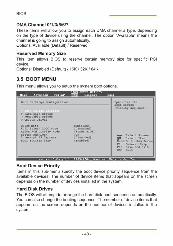
Items in this sub-menu specify the boot device priority sequence from the available devices. The number of device items that appears on the screen depends on the number of devices installed in the system.
Boot Device Priority
This menu allows you to setup the system boot options.3.5 BOOT MENU
BIOS SETUP UTILITYMain Advanced PCIPnP Boot Chipset
vxx.xx (C)Copyright 1985-200x, American Megatrends, Inc.
Select ScreenSelect ItemGo to Sub ScreenGeneral HelpSave and ExitExit
EnterF1F10ESC
Specifies theBoot DevicePriority sequence.
Boot Settings Configuration
> Hard Disk Drives> Removable Drives> CD/DVD Drives
Quick Boot [Enabled]Full Screen LOGO Show [Disabled]AddOn ROM Display Mode [Force BIOS]Bootup Num-Lock [On]Interrupt 19 Capture [Disabled]BOOT SUCCESS BEEP [Enabled]
> Boot Device Priority
Exit
The BIOS will attempt to arrange the hard disk boot sequence automatically. You can also change the booting sequence. The number of device items that appears on the screen depends on the number of devices installed in the system.
Hard Disk Drives
BIOS
- 44 -
The BIOS will attempt to arrange the removable drive boot sequence automatically. You can also change the booting sequence. The number of device items that appears on the screen depends on the number of devices installed in the system.
This item allows you to enable/disable Full Screen LOGO Show function.Options: Disabled (Default) / Enabled
Removable Drives
Full Screen LOGO Show
The BIOS will attempt to arrange the CD/DVD drive boot sequence automatically. You can also change the booting sequence. The number of device items that appears on the screen depends on the number of devices installed in the system.
This item sets the display mode for option ROM.Options: Force BIOS (Default) / Keep Current
Interrupt 19 is the software interrupt that handles the boot disk function. When set to Enabled, this item allows the option ROMs to trap interrupt 19.Options: Disabled (Default) / Enabled
CD/DVD Drives
AddOn ROM Display Mode
Interrupt 19 Capture
Enabling this option will cause an abridged version of the Power On Self-Test (POST) to execute after you power up the computer.Options: Enabled (Default) / Disabled
Selects the NumLock State after the system is switched on.Options: On (Default) / Off
When this item is set to Enabled, BIOS will let user know boot success with beep. Options: Enabled (Default) / Disabled
Quick Boot
Bootup Num-Lock
BOOT SUCCESS BEEP
BIOS
- 45 -
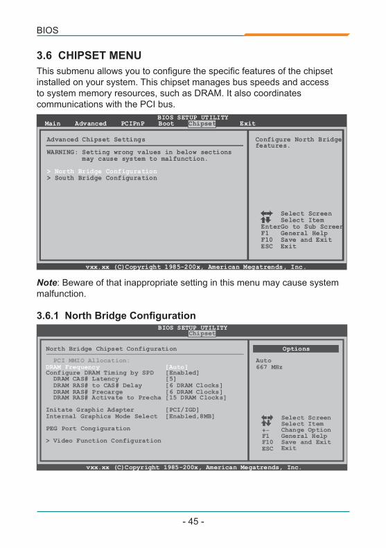
This submenu allows you to configure the specific features of the chipset installed on your system. This chipset manages bus speeds and access to system memory resources, such as DRAM. It also coordinates communications with the PCI bus.
3.6 CHIPSET MENU
BIOS SETUP UTILITYMain Advanced PCIPnP Boot Chipset
vxx.xx (C)Copyright 1985-200x, American Megatrends, Inc.
Select ScreenSelect ItemGo to Sub ScreenGeneral HelpSave and ExitExit
EnterF1F10ESC
Advanced Chipset Settings
WARNING: Setting wrong values in below sections may cause system to malfunction.
> South Bridge Configuration> North Bridge Configuration
Exit
Configure North Bridgefeatures.
Note: Beware of that inappropriate setting in this menu may cause system malfunction.
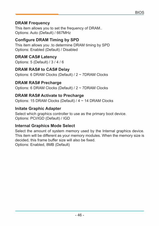
3.6.1 North Bridge ConfigurationBIOS SETUP UTILITY
Chipset
vxx.xx (C)Copyright 1985-200x, American Megatrends, Inc.
Select ScreenSelect ItemChange OptionGeneral HelpSave and ExitExit
+-F1F10ESC
North Bridge Chipset Configuration
PEG Port Congiguration
Configure DRAM Timing by SPD [Enabled] DRAM CAS# Latency [5] DRAM RAS# to CAS# Delay [6 DRAM Clocks] DRAM RAS# Precarge [6 DRAM Clocks] DRAM RAS# Activate to Precha [15 DRAM Clocks]
Initate Graphic Adapter [PCI/IGD]Internal Graphics Mode Select [Enabled,8MB]
> Video Function Configuration
PCI MMIO Allocation:DRAM Frequency [Auto]
Options
Auto667 MHz
BIOS
- 46 -
This item allows you to set the frequency of DRAM..Options: Auto (Default) / 667MHz
Options: 6 DRAM Clocks (Default) / 2 ~ 7DRAM Clocks
DRAM Frequency
DRAM RAS# to CAS# Delay
This item allows you .to determine DRAM timing by SPDOptions: Enabled (Default) / Disabled
Options: 6 DRAM Clocks (Default) / 2 ~ 7DRAM Clocks
Select which graphics controller to use as the primary boot device.Options: PCI/IGD (Default) / IGD
Configure DRAM Timing by SPD
DRAM RAS# Precharge
Initate Graphic Adapter
Options: 5 (Default) / 3 / 4 / 6
Options: 15 DRAM Clocks (Default) / 4 ~ 14 DRAM Clocks
Select the amount of system memory used by the Internal graphics device. This item will be different as your memory modules. When the memory size is decided, this frame buffer size will also be fixed.Options: Enabled, 8MB (Default)
DRAM CAS# Latency
DRAM RAS# Activate to Precharge
Internal Graphics Mode Select
BIOS
- 47 -
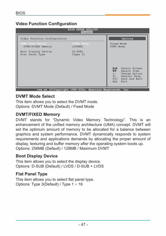
This item allows you to select the DVMT mode.Options: DVMT Mode (Default) / Fixed Mode
This item allows you to select the display device.Options: D-SUB (Default) / LVDS / D-SUB + LVDS
DVMT Mode Select
Boot Display Device
DVMT stands for “Dynamic Video Memory Technology”. This is an enhancement of the unified memory architecture (UMA) concept. DVMT will set the optimum amount of memory to be allocated for a balance between graphics and system performance. DVMT dynamically responds to system requirements and applications demands by allocating the proper amount of display, texturing and buffer memory after the operating system boots up.Options: 256MB (Default) / 128MB / Maximum DVMT
This item allows you to select flat panel type.Options: Type 3(Default) / Type 1 ~ 16
DVMT/FIXED Memory
Flat Panel Type
Video Function ConfigurationBIOS SETUP UTILITY
Chipset
vxx.xx (C)Copyright 1985-200x, American Megatrends, Inc.
Select ScreenSelect ItemChange OptionGeneral HelpSave and ExitExit
+-F1F10ESC
Video Function Configuration
DVMT/FIXED Memory [256MB]
Boot Display Device [D-SUB]Flat Panel Type [Type 3]
DVMT Mode Select [DVMT Mode]
Options
Fixed ModeDVMT Mode
BIOS
- 48 -
3.6.2 South Bridge ConfigurationBIOS SETUP UTILITY
Chipset
vxx.xx (C)Copyright 1985-200x, American Megatrends, Inc.
Select ScreenSelect ItemChange OptionGeneral HelpSave and ExitExit
+-F1F10ESC
North Bridge Chipset Configuration
PEG Port Congiguration
Configure DRAM Timing by SPD [Enabled] DRAM CAS# Latency [5] DRAM RAS# to CAS# Delay [6 DRAM Clocks] DRAM RAS# Precarge [6 DRAM Clocks] DRAM RAS# Activate to Precha [15 DRAM Clocks]
Initate Graphic Adapter [PCI/IGD]Internal Graphics Mode Select [Enabled,8MB]
> Video Function Configuration
PCI MMIO Allocation:DRAM Frequency [Auto]
Options
Auto667 MHz
The item determines the activation of USB port.Options: 10 USB Ports (Default) / 2 USB Ports / 4 USB Ports / 6 USB Ports /8 USB Port / Disabled
This BIOS feature controls the I/O buffers for the SMBus.Options: Enabled (Default) / Disabled
USB Functions
SMBUS Controller
This entry is only used to enable/disable EHCI controller. The BIOS itself may/may not have high speed USB support. If the BIOS has high speedUSB support, the controller will be automatically turned on when high speeddevices are connected.Options: Enabled (Default) / Disabled
Options : 1 to 2 seconds (Default) / 4 to 5 seconds / 3 to 4 seconds / 2 to 3seconds
USB 2.0 Controller
SLP_S4# Min. Assertion Width
This item allows you to control the Audio support.Options: Enabled (Default) / Disabled
This item allows you to enable or disable the Onboard LAN.Options : Enabled (Default) / Disabled
HDA Controller
Onboard LAN 1/2
BIOS
- 49 -
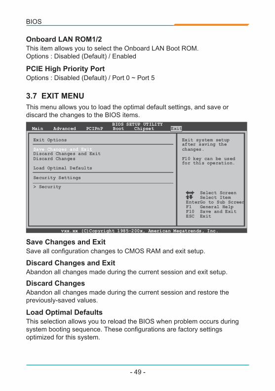
Abandon all changes made during the current session and exit setup.Discard Changes and Exit
Abandon all changes made during the current session and restore thepreviously-saved values.
This item allows you to select the Onboard LAN Boot ROM.Options : Disabled (Default) / Enabled
Discard Changes
Onboard LAN ROM1/2
Save all configuration changes to CMOS RAM and exit setup.
This selection allows you to reload the BIOS when problem occurs duringsystem booting sequence. These configurations are factory settingsoptimized for this system.
Options : Disabled (Default) / Port 0 ~ Port 5
Save Changes and Exit
Load Optimal Defaults
PCIE High Priority Port
This menu allows you to load the optimal default settings, and save ordiscard the changes to the BIOS items.
3.7 EXIT MENU
BIOS SETUP UTILITYMain Advanced PCIPnP Boot Chipset
vxx.xx (C)Copyright 1985-200x, American Megatrends, Inc.
Select ScreenSelect ItemGo to Sub ScreenGeneral HelpSave and ExitExit
EnterF1F10ESC
Exit system setupafter saving thechanges.
F10 key can be usedfor this operation.
Exit Options
Security Settings
Save Changes and ExitDiscard Changes and ExitDiscard Changes
Load Optimal Defaults
> Security
Exit
BIOS
- 50 -
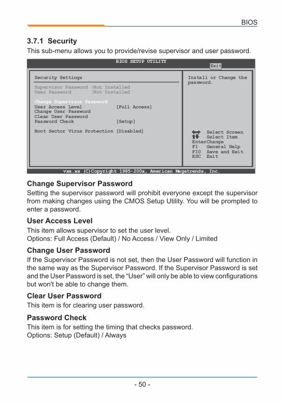
This sub-menu allows you to provide/revise supervisor and user password.3.7.1 Security
BIOS SETUP UTILITY
vxx.xx (C)Copyright 1985-200x, American Megatrends, Inc.
Select ScreenSelect ItemChangeGeneral HelpSave and ExitExit
EnterF1F10ESC
Install or Change thepassword.
Security Settings
Supervisor Password :Not InstalledUser Password :Not Installed
Change Supervisor PasswordUser Access Level [Full Access]Change User PasswordClear User PasswordPassword Check [Setup]
Boot Sector Virus Protection [Disabled]
Exit
Setting the supervisor password will prohibit everyone except the supervisor from making changes using the CMOS Setup Utility. You will be prompted to enter a password.
This item is for clearing user password.
Change Supervisor Password
Clear User Password
This item allows supervisor to set the user level.Options: Full Access (Default) / No Access / View Only / Limited
This item is for setting the timing that checks password.Options: Setup (Default) / Always
User Access Level
Password Check
If the Supervisor Password is not set, then the User Password will function in the same way as the Supervisor Password. If the Supervisor Password is set and the User Password is set, the “User” will only be able to view configurations but won't be able to change them.
Change User Password

BIOS
- 51 -
This option allows you to choose the VIRUS Warning feature that is used to protect the IDE Hard Disk boot sector. If this function is enabled and an attempt is made to write to the boot sector, BIOS will display a warning message on the screen and sound an alarm beep.Options: Disabled (Default) / Enabled
Boot Sector Virus Protection

This page is intentionally left blank.

Appendix
- 53 -
Appendix
Useful Help
Appendix - Useful Help
Appendix
- 54 -
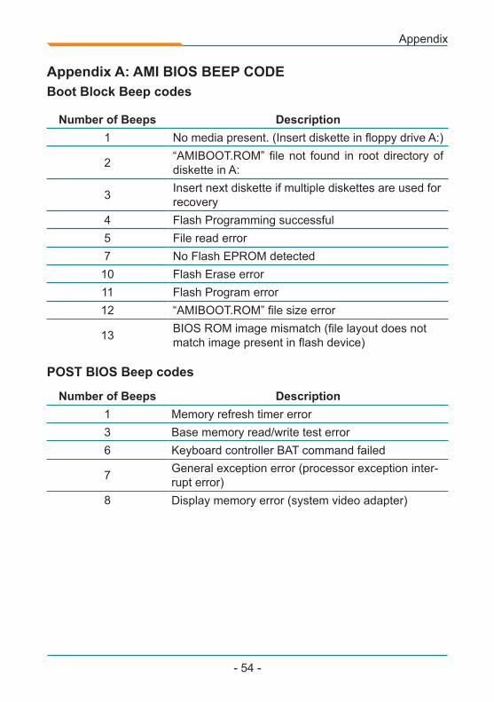
Appendix A: AMI BIOS BEEP CODE
Number of Beeps Description1 No media present. (Insert diskette in floppy drive A:)
2 “AMIBOOT.ROM” file not found in root directory of diskette in A:
3 Insert next diskette if multiple diskettes are used for recovery
4 Flash Programming successful5 File read error7 No Flash EPROM detected10 Flash Erase error11 Flash Program error12 “AMIBOOT.ROM” file size error
13 BIOS ROM image mismatch (file layout does not match image present in flash device)
Boot Block Beep codes
POST BIOS Beep codes
Number of Beeps Description1 Memory refresh timer error3 Base memory read/write test error6 Keyboard controller BAT command failed
7 General exception error (processor exception inter-rupt error)
8 Display memory error (system video adapter)
Appendix
- 55 -
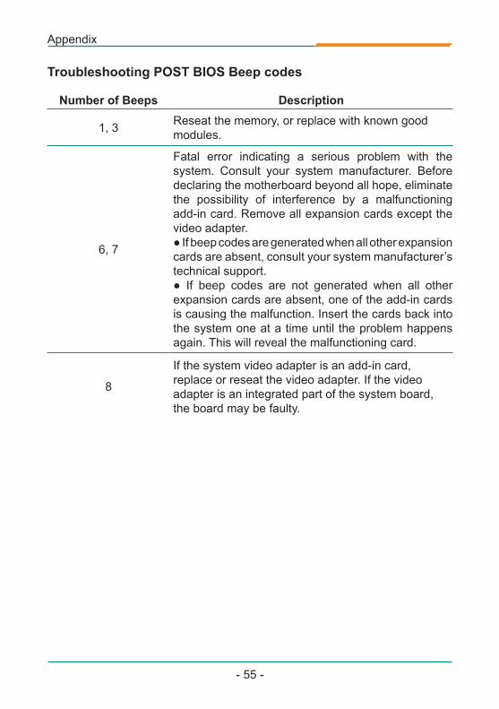
Troubleshooting POST BIOS Beep codes
Number of Beeps Description
1, 3 Reseat the memory, or replace with known good modules.
6, 7
Fatal error indicating a serious problem with the system. Consult your system manufacturer. Before declaring the motherboard beyond all hope, eliminate the possibility of interference by a malfunctioning add-in card. Remove all expansion cards except the video adapter.● If beep codes are generated when all other expansion cards are absent, consult your system manufacturer’s technical support.● If beep codes are not generated when all other expansion cards are absent, one of the add-in cards is causing the malfunction. Insert the cards back into the system one at a time until the problem happens again. This will reveal the malfunctioning card.
8
If the system video adapter is an add-in card, replace or reseat the video adapter. If the video adapter is an integrated part of the system board, the board may be faulty.
Appendix
- 56 -
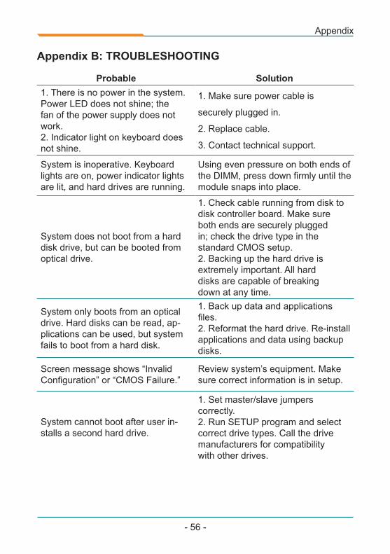
Probable Solution1. There is no power in the system.Power LED does not shine; thefan of the power supply does notwork.2. Indicator light on keyboard doesnot shine.
1. Make sure power cable is
securely plugged in.
2. Replace cable.
3. Contact technical support.
System is inoperative. Keyboard lights are on, power indicator lights are lit, and hard drives are running.
Using even pressure on both ends ofthe DIMM, press down firmly until themodule snaps into place.
System does not boot from a hard disk drive, but can be booted from optical drive.
1. Check cable running from disk todisk controller board. Make sureboth ends are securely pluggedin; check the drive type in thestandard CMOS setup.2. Backing up the hard drive isextremely important. All harddisks are capable of breakingdown at any time.
System only boots from an opticaldrive. Hard disks can be read, ap-plications can be used, but system fails to boot from a hard disk.
1. Back up data and applicationsfiles.2. Reformat the hard drive. Re-install applications and data using backup disks.
Screen message shows “InvalidConfiguration” or “CMOS Failure.”
Review system’s equipment. Make sure correct information is in setup.
System cannot boot after user in-stalls a second hard drive.
1. Set master/slave jumperscorrectly.2. Run SETUP program and selectcorrect drive types. Call the drivemanufacturers for compatibilitywith other drives.
Appendix B: TROUBLESHOOTING

Appendix
- 57 -
This page is intentionally left blank.