Power MOSFET 2017: Market and Technology Trends - 2017 Report by Yole Developpement
ITRS MOSFET Scaling Trends, Challenges, and Key Technology InnovationsITRS MOSFET Scaling Trends, Challenges, and ITRS MOSFET Scaling Trends, Challenges, and Key Technology InnovationsKey Technology Innovations
Workshop on Frontiers of Extreme Computing
Santa Cruz, CA
October 24, 2005
Peter M. Zeitzoff
2
Outline
• Introduction
• MOSFET scaling and its impact
• Material and process approaches and solutions
• Non-classical CMOS
• Conclusions
SEMATECH, the SEMATECH logo, AMRC, Advanced Materials Research Center, ATDF, the ATDF logo, Advanced
Technology Development Facility, ISMI and International SEMATECH Manufacturing Initiative are servicemarks of
SEMATECH, Inc. All other servicemarks and trademarks are the property of their respective owners.
3
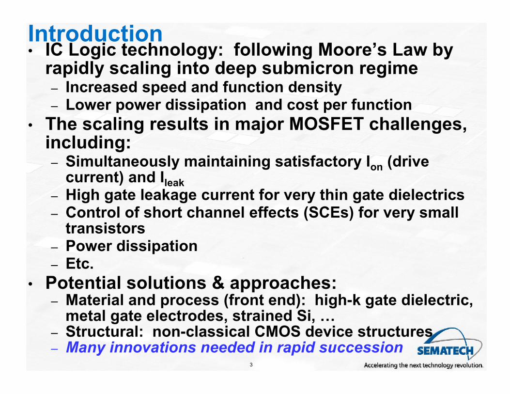
Introduction• IC Logic technology: following Moore’s Law by rapidly scaling into deep submicron regime – Increased speed and function density– Lower power dissipation and cost per function
• The scaling results in major MOSFET challenges, including:– Simultaneously maintaining satisfactory Ion (drive current) and Ileak
– High gate leakage current for very thin gate dielectrics– Control of short channel effects (SCEs) for very small transistors
– Power dissipation– Etc.
• Potential solutions & approaches:– Material and process (front end): high-k gate dielectric, metal gate electrodes, strained Si, …
– Structural: non-classical CMOS device structures– Many innovations needed in rapid succession
4
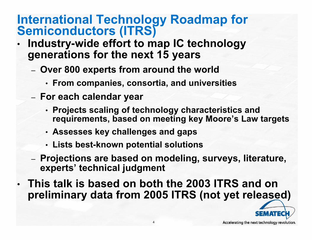
International Technology Roadmap for Semiconductors (ITRS)• Industry-wide effort to map IC technology generations for the next 15 years
– Over 800 experts from around the world
• From companies, consortia, and universities
– For each calendar year
• Projects scaling of technology characteristics and requirements, based on meeting key Moore’s Law targets
• Assesses key challenges and gaps
• Lists best-known potential solutions
– Projections are based on modeling, surveys, literature, experts’ technical judgment
• This talk is based on both the 2003 ITRS and on preliminary data from 2005 ITRS (not yet released)
5
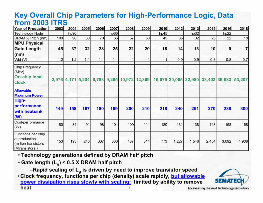
Year of Production 2003 2004 2005 2006 2007 2008 2009 2010 2012 2013 2015 2016 2018
Technology Node hp90 hp65 hp45 hp32 hp22
DRAM ½ Pitch (nm) 100 90 80 70 65 57 50 45 35 32 25 22 18
MPU Physical
Gate Length
(nm)
45 37 32 28 25 22 20 18 14 13 10 9 7
Vdd (V) 1.2 1.2 1.1 1.1 1.1 1 1 1 0.9 0.9 0.8 0.8 0.7
Chip Frequency
(MHz)
On-chip local
clock2,976 4,171 5,204 6,783 9,285 10,972 12,369 15,079 20,065 22,980 33,403 39,683 53,207
Allowable
Maximum Power
High-
performance
with heatsink
(W)
149 158 167 180 189 200 210 218 240 251 270 288 300
Cost-performance
(W)80 84 91 98 104 109 114 120 131 138 148 158 168
Functions per chip
at production
(million transistors
[Mtransistors])
153 193 243 307 386 487 614 773 1,227 1,546 2,454 3,092 4,908
Key Overall Chip Parameters for High-Performance Logic, Data from 2003 ITRS
• Technology generations defined by DRAM half pitch
• Gate length (Lg) ≤≤≤≤ 0.5 X DRAM half pitch
–Rapid scaling of Lg is driven by need to improve transistor speed
• Clock frequency, functions per chip (density) scale rapidly, but allowable power dissipation rises slowly with scaling: limited by ability to remove heat
6
Outline
• Introduction
• MOSFET scaling and its impact
• Material and process approaches
and solutions
• Non-classical CMOS
• Conclusions
7
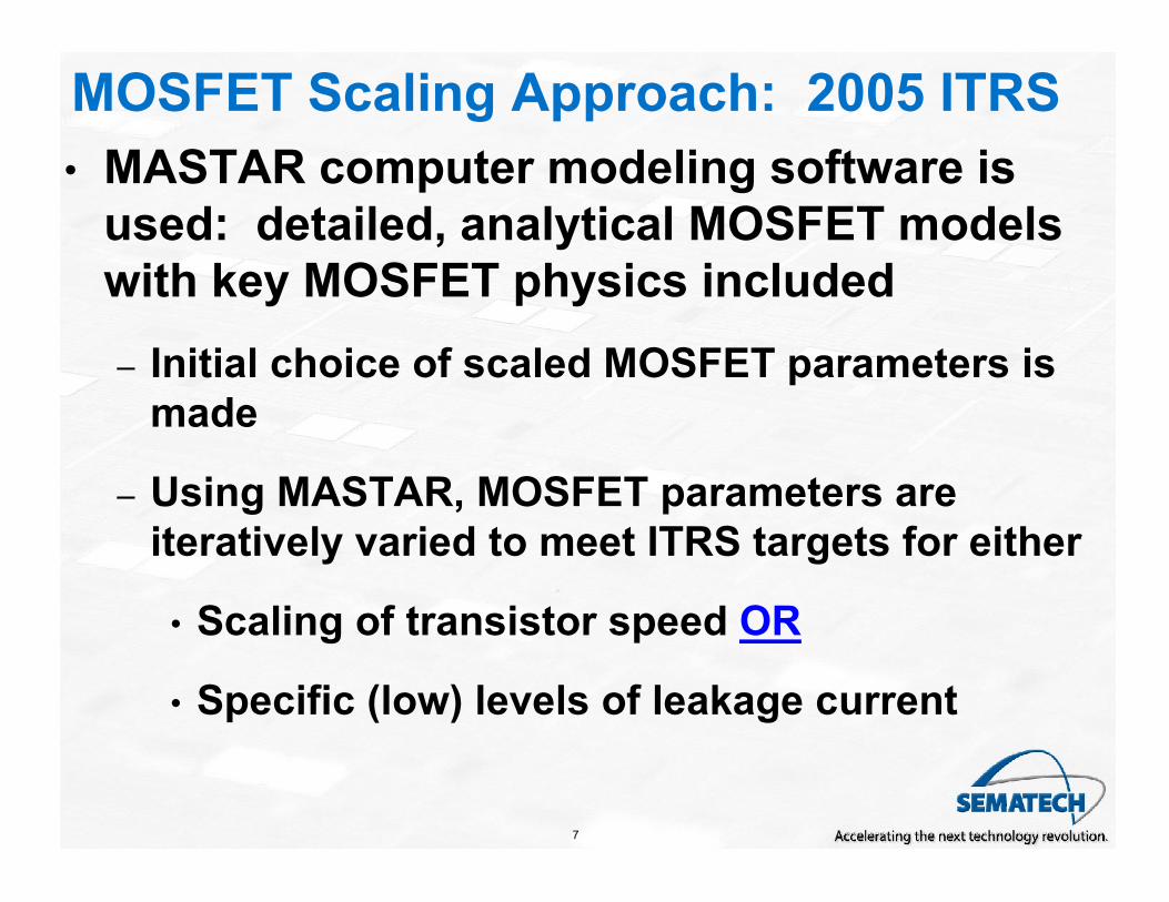
MOSFET Scaling Approach: 2005 ITRS
• MASTAR computer modeling software is
used: detailed, analytical MOSFET models
with key MOSFET physics included
– Initial choice of scaled MOSFET parameters is
made
– Using MASTAR, MOSFET parameters are
iteratively varied to meet ITRS targets for either
• Scaling of transistor speed OR
• Specific (low) levels of leakage current
8
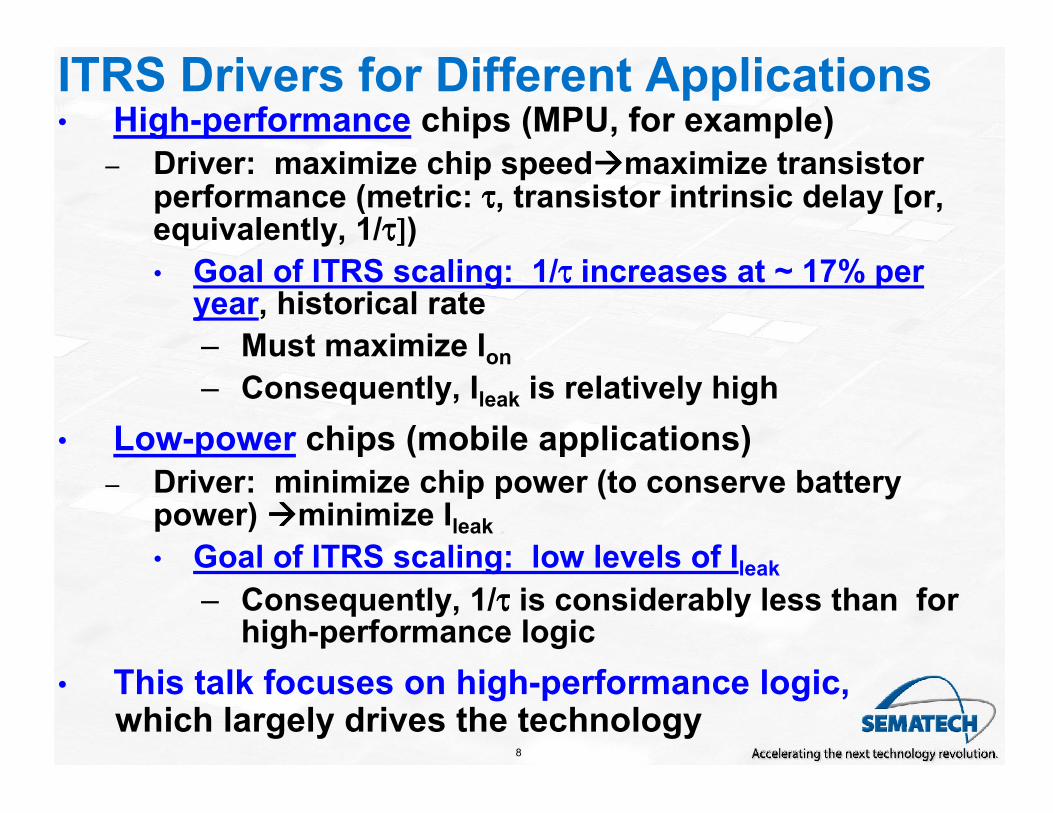
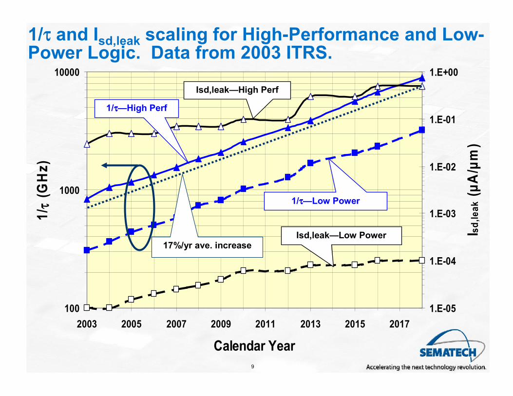
ITRS Drivers for Different Applications• High-performance chips (MPU, for example)
– Driver: maximize chip speed����maximize transistor performance (metric: ττττ, transistor intrinsic delay [or, equivalently, 1/τ]τ]τ]τ])
• Goal of ITRS scaling: 1/ττττ increases at ~ 17% per year, historical rate
– Must maximize Ion– Consequently, Ileak is relatively high
• Low-power chips (mobile applications)
– Driver: minimize chip power (to conserve battery power) ����minimize Ileak• Goal of ITRS scaling: low levels of Ileak
– Consequently, 1/ττττ is considerably less than for high-performance logic
• This talk focuses on high-performance logic,which largely drives the technology
9
1/ττττ and Isd,leak scaling for High-Performance and Low-Power Logic. Data from 2003 ITRS.
100
1000
10000
2003 2005 2007 2009 2011 2013 2015 2017
Calendar Year
1/ τ
τ
τ
τ
(GHz)
1.E-05
1.E-04
1.E-03
1.E-02
1.E-01
1.E+00
I sd,leak (µA/µm)
Isd,leak—High Perf
1/ττττ—High Perf
Isd,leak—Low Power
1/ττττ—Low Power
17%/yr ave. increase
10
1
10
100
1000
10000
2003 2005 2007 2009 2011 2013 2015 2017
Calendar Year
1/tau (GHz)
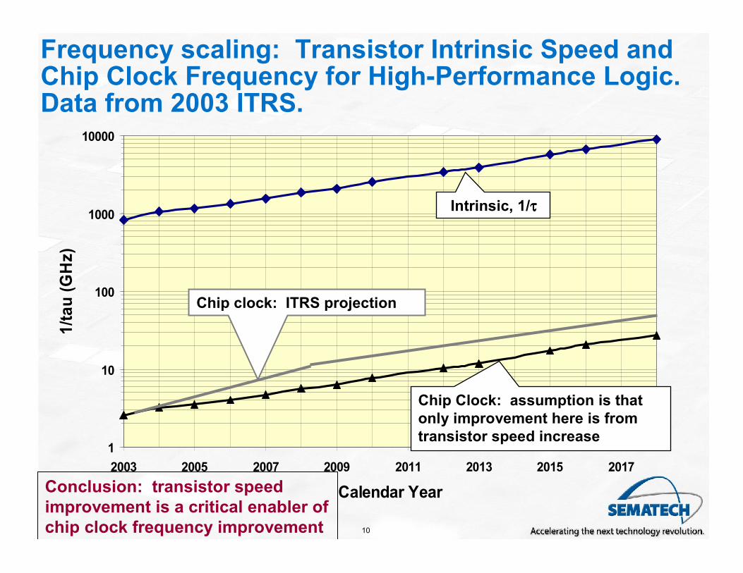
Intrinsic, 1/ττττ
Chip Clock: assumption is that
only improvement here is from
transistor speed increase
Frequency scaling: Transistor Intrinsic Speed and Chip Clock Frequency for High-Performance Logic. Data from 2003 ITRS.
Chip clock: ITRS projection
Conclusion: transistor speed
improvement is a critical enabler of
chip clock frequency improvement
11
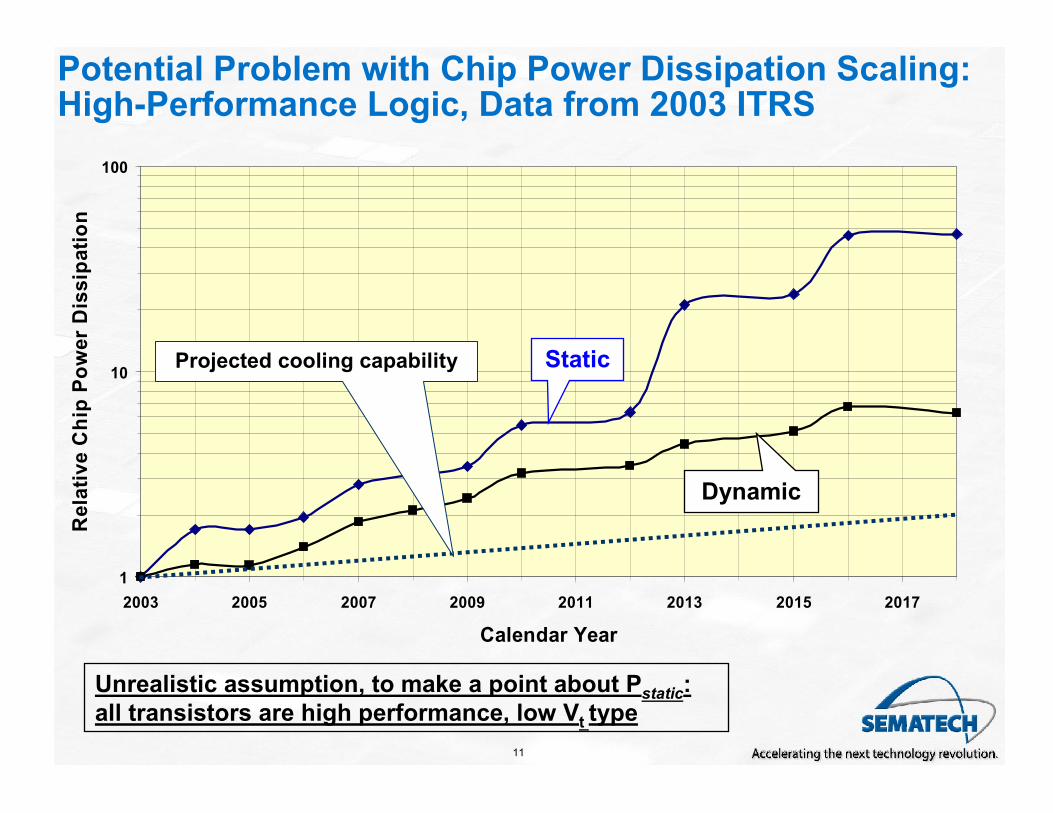
Potential Problem with Chip Power Dissipation Scaling: High-Performance Logic, Data from 2003 ITRS
1
10
100
2003 2005 2007 2009 2011 2013 2015 2017
Calendar Year
Relative Chip Power Dissipation
Static
Dynamic
Unrealistic assumption, to make a point about Pstatic:
all transistors are high performance, low Vt type
Projected cooling capability
12
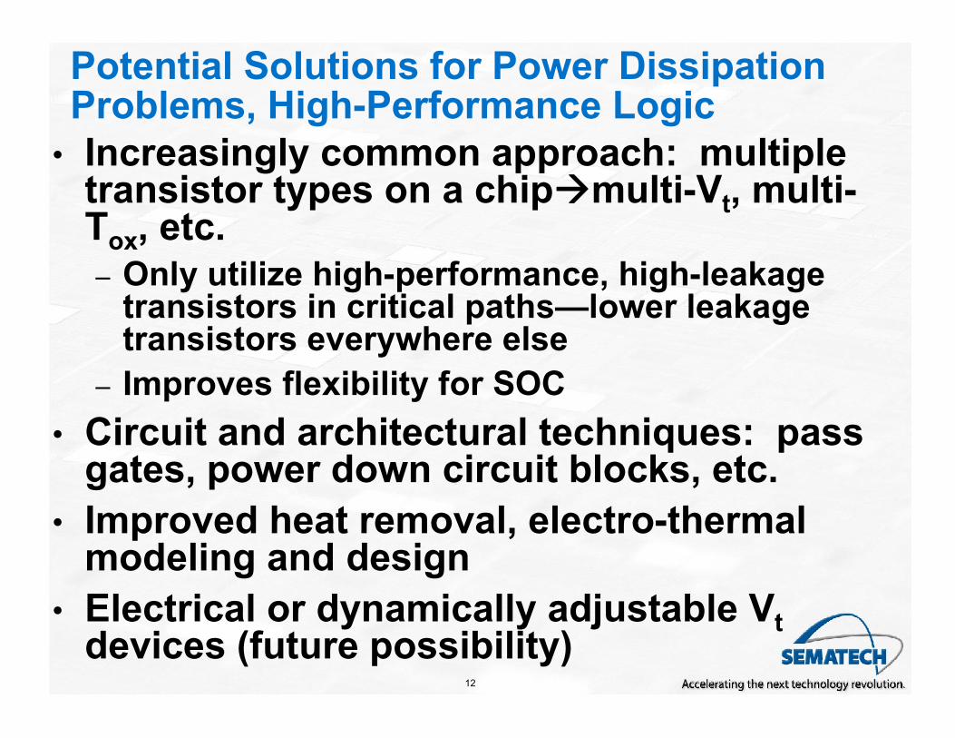
Potential Solutions for Power Dissipation Problems, High-Performance Logic
• Increasingly common approach: multiple transistor types on a chip����multi-Vt, multi-Tox, etc.
– Only utilize high-performance, high-leakage transistors in critical paths—lower leakage transistors everywhere else
– Improves flexibility for SOC
• Circuit and architectural techniques: pass gates, power down circuit blocks, etc.
• Improved heat removal, electro-thermal modeling and design
• Electrical or dynamically adjustable Vtdevices (future possibility)
13
Outline
• Introduction
• MOSFET scaling and its impact
• Material and process approaches
and solutions
• Non-classical CMOS
• Conclusions
14
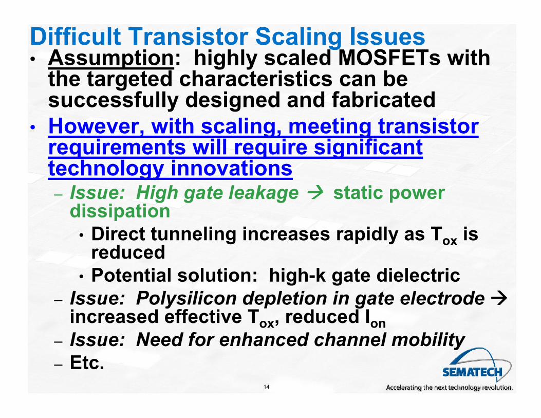
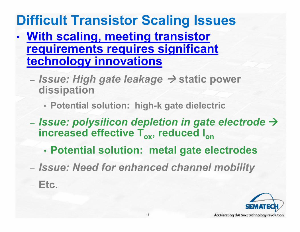
Difficult Transistor Scaling Issues• Assumption: highly scaled MOSFETs with the targeted characteristics can be successfully designed and fabricated
• However, with scaling, meeting transistor requirements will require significant technology innovations– Issue: High gate leakage ���� static power dissipation
• Direct tunneling increases rapidly as Tox is reduced
• Potential solution: high-k gate dielectric
– Issue: Polysilicon depletion in gate electrode ����increased effective Tox, reduced Ion
– Issue: Need for enhanced channel mobility
– Etc.
15
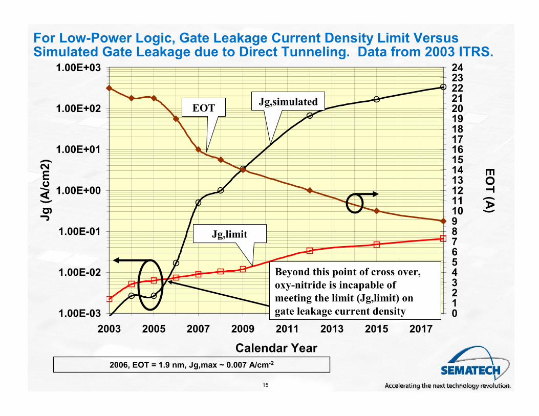
For Low-Power Logic, Gate Leakage Current Density Limit Versus Simulated Gate Leakage due to Direct Tunneling. Data from 2003 ITRS.
1.00E-03
1.00E-02
1.00E-01
1.00E+00
1.00E+01
1.00E+02
1.00E+03
2003 2005 2007 2009 2011 2013 2015 2017
Calendar Year
Jg (A/cm2)
0123456789101112131415161718192021222324
EOT (A
)
Jg,simulated
Jg,limit
EOT
2006, EOT = 1.9 nm, Jg,max ~ 0.007 A/cm-2
Beyond this point of cross over,
oxy-nitride is incapable of
meeting the limit (Jg,limit) on
gate leakage current density
16
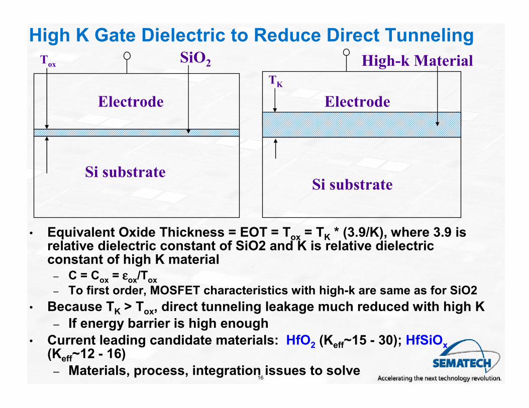
High K Gate Dielectric to Reduce Direct Tunneling
• Equivalent Oxide Thickness = EOT = Tox = TK * (3.9/K), where 3.9 is relative dielectric constant of SiO2 and K is relative dielectric constant of high K material
– C = Cox = εεεεox/Tox
– To first order, MOSFET characteristics with high-k are same as for SiO2
• Because TK > Tox, direct tunneling leakage much reduced with high K
– If energy barrier is high enough
• Current leading candidate materials: HfO2 (Keff~15 - 30); HfSiOx
(Keff~12 - 16)
– Materials, process, integration issues to solve
Electrode
Si substrate
ToxSiO2
TK
High-k Material
Electrode
Si substrate
17
Difficult Transistor Scaling Issues• With scaling, meeting transistor requirements requires significant technology innovations
– Issue: High gate leakage ���� static power dissipation
• Potential solution: high-k gate dielectric
– Issue: polysilicon depletion in gate electrode ����increased effective Tox, reduced Ion
• Potential solution: metal gate electrodes
– Issue: Need for enhanced channel mobility
– Etc.
18
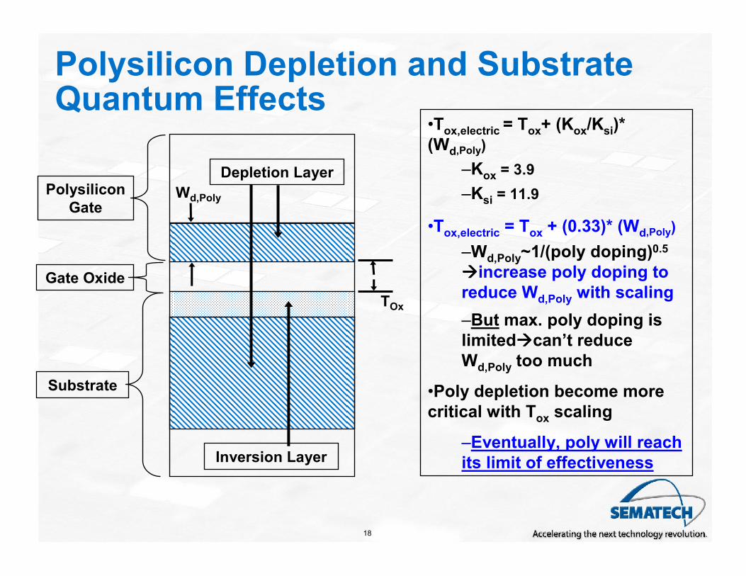
Polysilicon Depletion and Substrate Quantum Effects
•Tox,electric = Tox+ (Kox/Ksi)*
(Wd,Poly)
–Kox = 3.9
–Ksi = 11.9
•Tox,electric = Tox + (0.33)* (Wd,Poly)
–Wd,Poly~1/(poly doping)0.5
����increase poly doping to
reduce Wd,Poly with scaling
–But max. poly doping is
limited����can’t reduce
Wd,Poly too much
•Poly depletion become more
critical with Tox scaling
–Eventually, poly will reach
its limit of effectiveness
TOx
Polysilicon
Gate
Gate Oxide
Substrate
Depletion Layer
Inversion Layer
Wd,Poly
19
Metal Gate Electrodes
• Metal gate electrodes are a potential solution when poly “runs out of steam”: probably implemented in 2008 or beyond
– No depletion, very low resistance gate, no boron penetration, compatibility with high-k
– Issues
• Different work functions needed for PMOS and NMOS==>2 different metals may be needed
–Process complexity, process integration problems, cost
• Etching of metal electrodes
• New materials: major challenge
20
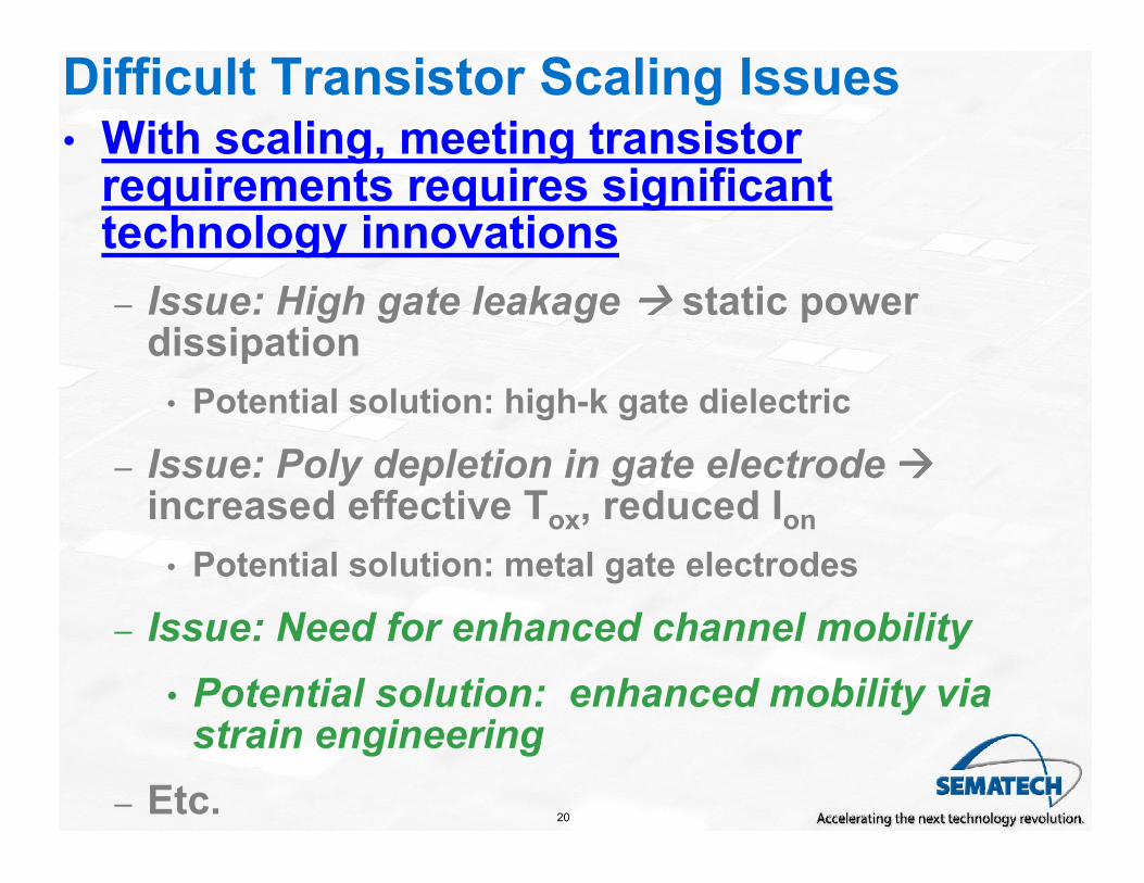
Difficult Transistor Scaling Issues• With scaling, meeting transistor requirements requires significant technology innovations
– Issue: High gate leakage ���� static power dissipation
• Potential solution: high-k gate dielectric
– Issue: Poly depletion in gate electrode ����increased effective Tox, reduced Ion
• Potential solution: metal gate electrodes
– Issue: Need for enhanced channel mobility
• Potential solution: enhanced mobility via strain engineering
– Etc.
21
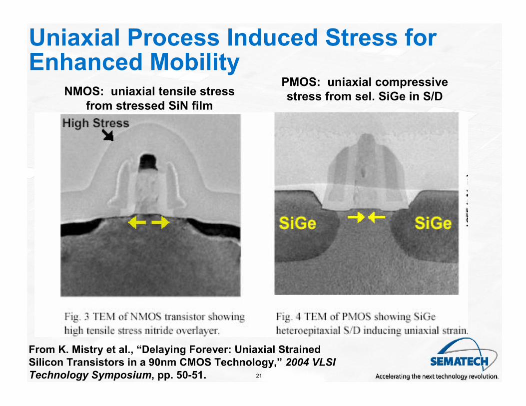
Uniaxial Process Induced Stress for Enhanced Mobility
From K. Mistry et al., “Delaying Forever: Uniaxial Strained
Silicon Transistors in a 90nm CMOS Technology,” 2004 VLSI
Technology Symposium, pp. 50-51.
NMOS: uniaxial tensile stress
from stressed SiN film
PMOS: uniaxial compressive
stress from sel. SiGe in S/D
22
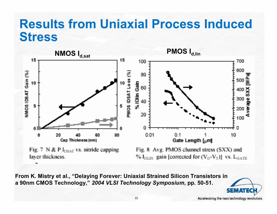
Results from Uniaxial Process Induced Stress
From K. Mistry et al., “Delaying Forever: Uniaxial Strained Silicon Transistors in
a 90nm CMOS Technology,” 2004 VLSI Technology Symposium, pp. 50-51.
NMOS Id,satPMOS Id,lin
23
Outline
• Introduction
• Scaling and its impact
• Material and process approaches
and solutions
• Non-classical CMOS
• Conclusions
24
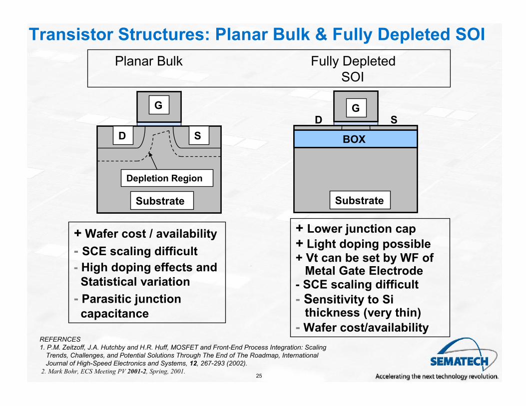
Limits of Scaling Planar, Bulk MOSFETs• 65 nm tech. generation (2007, Lg = 25nm) and beyond: increased difficulty in meeting all device requirements with classical planar, bulk CMOS (even with high-k, metal electrodes, strained Si…)
– Control of SCE
– Impact of quantum effects and statistical variation
– Impact of high substrate doping
– Control of series S/D resistance (Rseries,s/d)
– Others
• Alternative device structures (non-classical CMOS) may be utilized
– Ultra thin body, fully depleted: single-gate SOIand multiple-gate transistors
25
Transistor Structures: Planar Bulk & Fully Depleted SOI
REFERNCES
1. P.M. Zeitzoff, J.A. Hutchby and H.R. Huff, MOSFET and Front-End Process Integration: Scaling
Trends, Challenges, and Potential Solutions Through The End of The Roadmap, International
Journal of High-Speed Electronics and Systems, 12, 267-293 (2002).
2. Mark Bohr, ECS Meeting PV 2001-2, Spring, 2001.
Planar Bulk Fully Depleted
SOI
SD
G
Substrate
Depletion Region
+Wafer cost / availability
- SCE scaling difficult
- High doping effects and
Statistical variation
- Parasitic junction capacitance
+ Lower junction cap
+ Light doping possible+ Vt can be set by WF of Metal Gate Electrode
- SCE scaling difficult
- Sensitivity to Si thickness (very thin)
-Wafer cost/availability
Substrate
BOX
SDG
26
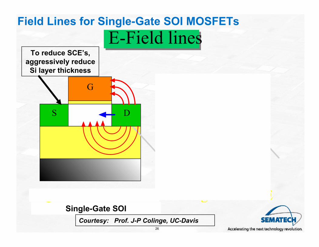
Field Lines for Single-Gate SOI MOSFETs
Single-Gate SOI
Courtesy: Prof. J-P Colinge, UC-Davis
BOX BOX
S D
G
S D
G
G
E-Field lines
Regular SOI MOSFETDouble-gate MOSFET
To reduce SCE’s,
aggressively reduce
Si layer thickness
27
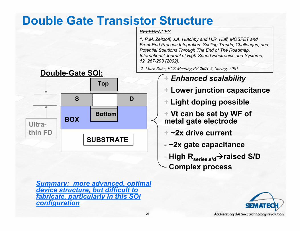
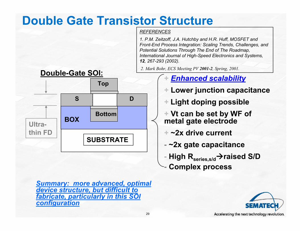
Double Gate Transistor Structure
+ Enhanced scalability
+ Lower junction capacitance
+ Light doping possible
+ Vt can be set by WF of metal gate electrode
+ ~2x drive current
- ~2x gate capacitance
- High Rseries,s/d����raised S/D
- Complex process
Ultra-
thin FD
S D
Top
Bottom
Double-Gate SOI:
BOX
SUBSTRATE
REFERENCES
1. P.M. Zeitzoff, J.A. Hutchby and H.R. Huff, MOSFET and
Front-End Process Integration: Scaling Trends, Challenges, and
Potential Solutions Through The End of The Roadmap,
International Journal of High-Speed Electronics and Systems,
12, 267-293 (2002).
2. Mark Bohr, ECS Meeting PV 2001-2, Spring, 2001.
Summary: more advanced, optimal device structure, but difficult to fabricate, particularly in this SOI configuration
28
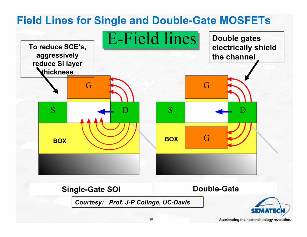
Field Lines for Single and Double-Gate MOSFETs
S D
G
S D
G
G
E-Field lines
Regular SOI MOSFET Double-gate MOSFET
Double gates
electrically shield
the channel
To reduce SCE’s,
aggressively
reduce Si layer
thickness
Single-Gate SOI Double-Gate
Courtesy: Prof. J-P Colinge, UC-Davis
BOX BOX
29
Double Gate Transistor Structure
+ Enhanced scalability
+ Lower junction capacitance
+ Light doping possible
+ Vt can be set by WF of metal gate electrode
+ ~2x drive current
- ~2x gate capacitance
- High Rseries,s/d����raised S/D
- Complex process
Ultra-
thin FD
S D
Top
Bottom
Double-Gate SOI:
BOX
SUBSTRATE
REFERENCES
1. P.M. Zeitzoff, J.A. Hutchby and H.R. Huff, MOSFET and
Front-End Process Integration: Scaling Trends, Challenges, and
Potential Solutions Through The End of The Roadmap,
International Journal of High-Speed Electronics and Systems,
12, 267-293 (2002).
2. Mark Bohr, ECS Meeting PV 2001-2, Spring, 2001.
Summary: more advanced, optimal device structure, but difficult to fabricate, particularly in this SOI configuration
30
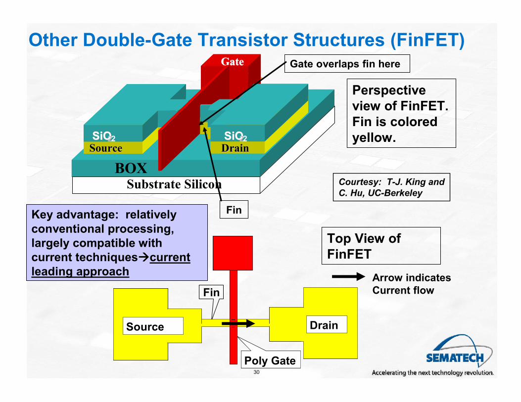
Other Double-Gate Transistor Structures (FinFET)
Poly GatePoly GatePoly GatePoly Gate
Source DrainSource DrainSource Drain
Fin
Source Drain
Top View of
FinFET
Arrow indicates
Current flow
Key advantage: relatively
conventional processing,
largely compatible with
current techniques����current
leading approach
Perspective
view of FinFET.
Fin is colored
yellow.
Gate overlaps fin here
SiO2
GateGate
DrainDrainSourceSourceSiOSiO22 SiOSiO22
SiO2
GateGate
DrainDrainSourceSourceSiOSiO22 SiOSiO22
SiO2
BOX
GateGate
DrainDrainSourceSourceSiOSiO22 SiOSiO22
Courtesy: T-J. King and
C. Hu, UC-Berkeley
Fin
Substrate Silicon
31
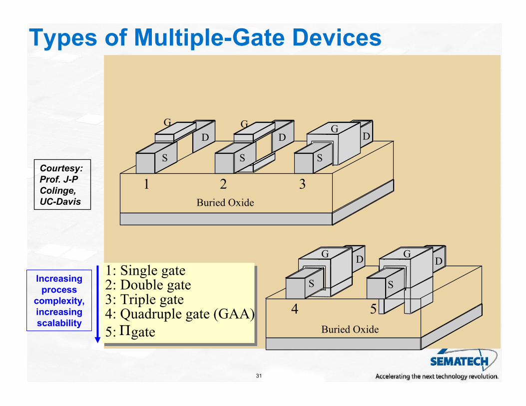
Types of Multiple-Gate Devices
S
D
G
S
D
G
S
DG
1 2 3
Buried Oxide
S
DG
S
DG
4 5
Buried Oxide
1: Single gate 2: Double gate 3: Triple gate 4: Quadruple gate (GAA)
5: Πgate
Courtesy:
Prof. J-P
Colinge,
UC-Davis
Increasing
process
complexity,
increasing
scalability
32
Outline
• Introduction
• Scaling and its impact
• Material and process approaches
and solutions
• Non-classical CMOS
• Conclusions
33
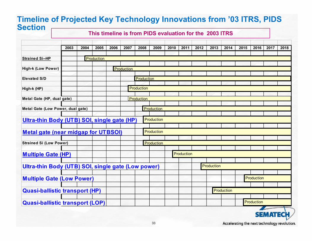
Timeline of Projected Key Technology Innovations from ’03 ITRS, PIDS Section
This timeline is from PIDS evaluation for the 2003 ITRS
2003 2004 2005 2006 2007 2008 2009 2010 2011 2012 2013 2014 2015 2016 2017 2018
Strained Si--HP
High-k (Low Power)
Elevated S/D
High-k (HP)
Metal Gate (HP, dual gate)
Metal Gate (Low Power, dual gate)
Ultra-thin Body (UTB) SOI, single gate (HP)
Metal gate (near midgap for UTBSOI)
Strained Si (Low Power)
Multiple Gate (HP)
Ultra-thin Body (UTB) SOI, single gate (Low power)
Multiple Gate (Low Power)
Quasi-ballistic transport (HP)
Quasi-ballistic transport (LOP)
Production
Production
Production
Production
Production
Production
Production
Production
Production
Production
Production
Production
Production
Production
34
Conclusions• Rapid transistor scaling is projected to continue through
the end of the Roadmap in 2020
– Transistor performance will improve rapidly, but leakage & SCEswill be difficult to control
• Transistor performance improvement is a key enabler of chip speed improvement
– Many technology innovations will be needed in a relatively shorttime to enable this rapid scaling
• Material and process innovations include high-k gate dielectric, metal gate electrodes, and enhanced mobility through strained silicon
– High-k and metal gate electrode needed in 2008
• Structural potential solutions: non-classical CMOS
• Non-classical CMOS and process and material innovations will likely be combined in the ultimate, end-of-Roadmap device
– Well under 10nm MOSFETs expected by the end of the Roadmap
• Power dissipation, especially static, is a growing problem with scaling: integrated, innovative approaches needed