ISL73096EH Total Dose Test Report - Intersil.com dose testing of the ISL73096EH radiation hardened...
15
1 Total dose testing of the ISL73096EH radiation hardened ultra high frequency NPN/PNP transistor array Nick van Vonno Intersil Corporation Revision 0 29 May 2014 Table of Contents 1. Introduction 2. Reference documents 3. Part description 4. Test description 4.1. Irradiation facility 4.2. Test fixturing 4.3. Characterization equipment and procedures 4.4. Experimental matrix 4.5. Downpoints 5. Results 5.1. Attributes data 5.2. Variables data 6. Conclusion 7. Appendices 8. Document revision history
Transcript of ISL73096EH Total Dose Test Report - Intersil.com dose testing of the ISL73096EH radiation hardened...

1
Total dose testing of the ISL73096EH radiation hardened ultra high frequency
NPN/PNP transistor array
Nick van Vonno
Intersil Corporation
Revision 0
29 May 2014
Table of Contents
1. Introduction
2. Reference documents
3. Part description
4. Test description
4.1. Irradiation facility
4.2. Test fixturing
4.3. Characterization equipment and procedures
4.4. Experimental matrix
4.5. Downpoints
5. Results
5.1. Attributes data
5.2. Variables data
6. Conclusion
7. Appendices
8. Document revision history

2
1. Introduction
This document reports the results of low and high dose rate total dose testing of the Intersil ISL73096EH
NPN/PNP transistor array. The test was performed in 2014 with the objective of providing an assessment of the low
dose rate hardness and dose rate sensitivity of the part. Parts were irradiated under bias and with all pins grounded at
low dose rate and under bias at high dose rate. The ISL73096EH is a five-transistor array comprising three NPN
transistors and two PNP transistors and is built in the Intersil UHF process, which uses bonded wafer dielectric
isolation technology. The DI process results in excellent isolation between transistors while retaining the thermal and
electrical matching advantages of single-die construction. The ISL73127RH and ISL73128RH are NPN only and PNP
only versions of the ISL73096EH; as the oxide thickness and doping levels are similar for all three parts are closely
similar, the present data is considered to apply to all three parts.
2. Reference Documents
MIL-STD-883 test method 1019.
ISL73096EH data sheet.
SMD 5962-07218.
3: Part Description
The ISL73096RH consists of three NPN transistors and two PNP transistors on a common substrate. The part is
built in a dielectrically isolated bonded wafer fabrication process providing single event latch-up (SEL) immunity,
while the high frequency vertical transistor structures provide excellent AC performance and total dose hardness.
The high gain-bandwidth product and low noise figure of these transistors make them ideal for use in high
frequency RF amplifier and mixer applications. Monolithic construction of the NPN and PNP transistors provides the
closest electrical and thermal matching possible. Access is provided to each terminal of each of the transistors for
maximum application flexibility.
Specifications for Rad Hard QML devices are controlled by the Defense Logistics Agency (DLA) in Columbus,
OH. The listed SMD numbers must be used when ordering. Detailed electrical specifications for these devices are
contained in SMD 5962-07218. A “hot-link” is provided on our website for downloading.
• QML qualified per MIL-PRF-38535 requirements
• Electrically screened to SMD # 5962-07218
- Total dose, high dose rate 3 x 10⁵rad(Si)
- SEL immune by process
• NPN gain bandwidth product (FT) 8GHz (typical)
• NPN current gain (hFE) 130 (typical)
• NPN Early voltage (VA) 50V (typical)
• PNP gain bandwidth product (FT) 5.5GHz (typical)
• PNP current gain (hFE) 60 (typical)
• PNP Early voltage (VA) 20V (typical)
• Noise figure (50Ω) at 1GHz 3.5dB (typical)
• Collector-to-collector leakage <1pA (typical)

3
4: Test Description
4.1 Irradiation Facilities
Low dose rate testing was performed at 0.01rad(Si)/s using the Intersil Palm Bay N40 (Hopewell Designs,
Alpharetta, GA) panoramic 60Co irradiator located in the Palm Bay, Florida facility. High dose rate testing was
performed at 65rad(Si)/s in a Gammacell 220 60Co irradiator located in the same facility.
4.2 Test Fixturing
Samples were irradiated under biased and grounded conditions (low dose rate samples) and under biased
conditions (high dose rate samples). Fig. 1 shows the configuration used for biased irradiation; the grounded
configuration simply grounds all pins and is not shown.
Figure 1: Irradiation bias configuration for the ISL73096EH. V1 = 5.5V +/- 0.5V; V2 = 10.5V +/-0.5V; R1,
R2, R3, R4 and R5 = 1.0kΩ +/- 5%; R6, R7, R8, R9 and R10 = 100.0Ω +/- 5%; and C1 through C10 = 0.01µF, 25V.
These devices feature an FT of 8GHz/5.5GHz and are heavily AC bypassed to insure stability.
4.3 Characterization equipment and procedures
All electrical testing was performed outside the irradiator using production automated test equipment (ATE)
with datalogging at each downpoint. Downpoint electrical testing was performed at room temperature only.
4.4 Experimental matrix
Total dose irradiation proceeded in accordance with the guidelines of MIL-STD-883 Test Method 1019.7. The
experimental matrix consisted of 24 samples irradiated at low dose rate under bias, 24 samples irradiated at low dose

4
rate with all pins grounded and 36 samples irradiated at high dose rate under bias. Several control units were used to
insure repeatable data at all downpoints.
Samples of the ISL73096EH were drawn from production fabrication lot DTJ6DB as part of the Intersil wafer
by wafer total dose acceptance testing program and were packaged in the hermetic 16-pin solder-sealed flatpack
(CDFP4-16) package. Samples were processed through the standard burnin cycle before irradiation, as required by
MIL-STD-883, and were screened to the ATE limits at room temperature prior to the test.
4.5 Downpoints
Downpoints for the biased and grounded low dose rate tests were zero, 10, 30 and 50krad(Si). The single
downpoint for the biased high dose rate test was 300krad(Si).
5. Test results
Testing at low and high dose rate of the ISL73096EH is complete. All monitored parameters were very stable
over both irradiation and anneals. Additionally, no transistor to transistor differences were noted, either in the pre-
irradiation data or in the total dose response of the parts, and no bias or dose rate sensitivity was noted.
5.2 Attributes data
Table 1: ISL73096EH low dose rate total dose test attributes data.
Part Dose rate (Note 1)
Bias Sample size
Downpoint Pass (Note 2)
Rejects
ISL73096EH LDR Biased 24 Pre-irradiation 24 0
10 krad(Si) 24 0
30 krad(Si) 24 0
50 krad(Si) 24 0
ISL73096EH LDR Grounded 24 Pre-irradiation 24 0
10 krad(Si) 24 0
30 krad(Si) 24 0
50 krad(Si) 24 0
ISL73096EH HDR Biased 36 Pre-irradiation 36
300 krad(Si) 36 0
Note 1: ‘LDR’ indicates low dose rate (0.01 rad(Si)/s); ‘HDR’ indicates high dose rate (50-300rad(Si)/s). Note 2: ‘Pass’ indicates a sample that passes all post-irradiation SMD limits.
5.2 Variables data
Figs. 2 through 21 plot the response of key parameters. In the plots, the individual transistors are designated as
NPN device 1 (‘Q1’) through device 3 (‘Q3’) and PNP device 4 (‘Q4’) and device 5 (‘Q5’).The NPN and PNP
devices are plotted separately, with Figs. 2 through 11 reporting the NPN data and Figs. 12 through 21 reporting the
PNP data. The plots show the average of key parameters as a function of low and high dose rate total dose for each of
the two irradiation conditions. We chose to plot the average for these parameters; the parametric distributions were
sufficiently tight that plotting them would have been difficult.

5
Fig. 2: ISL73096EH NPN collector-base breakdown voltage, emitter open (BVcbo), devices Q1 through Q3, plotted as a
function of low dose rate irradiation for the biased (per Figure 1) and unbiased (all pins grounded) cases and for high dose rate
irradiation for the biased (per Fig. 1) case. The low dose rate was 0.01 rad(Si)/s and the high dose rate was 65rad(Si)/s. Sample
size for the low dose rate cells was 24 and sample for the high dose rate cell was 36. The pre-irradiation SMD limit is 12.0V
minimum, while the post-irradiation SMD limit is also 12.0V minimum.
Fig. 3: ISL73096EH NPN collector-emitter breakdown voltage, base open (BVceo), devices Q1 through Q3, plotted as a
function of low dose rate irradiation for the biased (per Figure 1) and unbiased (all pins grounded) cases and for high dose rate
irradiation for the biased (per Fig. 1) case. The low dose rate was 0.01 rad(Si)/s and the high dose rate was 65rad(Si)/s. Sample
size for the low dose rate cells was 24 and sample for the high dose rate cell was 36. The pre-irradiation SMD limit is 8.0V
minimum, while the post-irradiation SMD limit is also 8.0V minimum.
10
15
20
25
30
0 50 100 150 200 250 300
NP
N B
Vc
bo
, V
Total dose, krad(Si)
Q1 LDR Bias Q2 LDR Bias
Q3 LDR Bias Q1 LDR GND
Q2 LDR GND Q3 LDR GND
Q1 HDR GND Q2 HDR GND
Q3 HDR GND Spec limit
0
5
10
15
20
25
30
0 50 100 150 200 250 300
NP
N B
Vc
eo
, V
Total dose, krad(Si)
Q1 LDR Bias Q2 LDR Bias
Q3 LDR Bias Q1 LDR GND
Q2 LDR GND Q3 LDR GND
Q1 HDR GND Q2 HDR GND
Q3 HDR GND Spec limit

6
Fig. 4: ISL73096EH NPN collector-emitter breakdown voltage, base shorted to emitter open (BVces), devices Q1 through Q3,
plotted as a function of low dose rate irradiation for the biased (per Figure 1) and unbiased (all pins grounded) cases and for high
dose rate irradiation for the biased (per Fig. 1) case. The low dose rate was 0.01 rad(Si)/s and the high dose rate was 65rad(Si)/s.
Sample size for the low dose rate cells was 24 and sample for the high dose rate cell was 36. The pre-irradiation SMD limit is
10.0V minimum, while the post-irradiation SMD limit is also 10.0V minimum.
Fig. 5: ISL73096EH NPN emitter-base breakdown voltage, collector open (BVebo), devices Q1 through Q3, plotted as a
function of low dose rate irradiation for the biased (per Figure 1) and unbiased (all pins grounded) cases and for high dose rate
irradiation for the biased (per Fig. 1) case. The low dose rate was 0.01 rad(Si)/s and the high dose rate was 65rad(Si)/s. Sample
size for the low dose rate cells was 24 and sample for the high dose rate cell was 36. The pre-irradiation SMD limit is 5.5V
minimum, while the post-irradiation SMD limit is also 5.5V minimum.
0
5
10
15
20
25
30
0 50 100 150 200 250 300
NP
N B
Vces
, V
Total dose, krad(Si)
Q1 LDR Bias Q2 LDR Bias
Q3 LDR Bias Q1 LDR GND
Q2 LDR GND Q3 LDR GND
Q1 HDR GND Q2 HDR GND
Q3 HDR GND Spec limit
0
2
4
6
8
0 50 100 150 200 250 300
NP
N B
Veb
o,
V
Total dose, krad(Si)
Q1 LDR Bias Q2 LDR Bias
Q3 LDR Bias Q1 LDR GND
Q2 LDR GND Q3 LDR GND
Q1 HDR GND Q2 HDR GND
Q3 HDR GND Spec limit

7
Fig. 6: ISL73096EH NPN common-emitter current gain (Hfe) at Ic = 10.0mA and Vce = 2.0V, devices Q1 through Q3, plotted
as a function of low dose rate irradiation for the biased (per Figure 1) and unbiased (all pins grounded) cases and for high dose
rate irradiation for the biased (per Fig. 1) case. The low dose rate was 0.01 rad(Si)/s and the high dose rate was 65rad(Si)/s.
Sample size for the low dose rate cells was 24 and sample for the high dose rate cell was 36. The pre-irradiation SMD limit is 80
minimum, while the post-irradiation SMD limit is 40 minimum. Current gain is a dimensionless parameter.
Fig.7: ISL73096EH NPN Early voltage (VA), devices Q1 through Q3, plotted as a function of low dose rate irradiation for the
biased (per Figure 1) and unbiased (all pins grounded) cases and for high dose rate irradiation for the biased (per Fig. 1) case.
The low dose rate was 0.01 rad(Si)/s and the high dose rate was 65rad(Si)/s. Sample size for the low dose rate cells was 24 and
sample for the high dose rate cell was 36.The pre-irradiation SMD limit is 20.0V minimum, while the post-irradiation SMD limit
is also 20.0V minimum.
20
40
60
80
100
120
140
0 50 100 150 200 250 300
NP
N H
fe
Total dose, krad(Si)
Q1 LDR Bias Q2 LDR Bias
Q3 LDR Bias Q1 LDR GND
Q2 LDR GND Q3 LDR GND
Q1 HDR GND Q2 HDR GND
Q3 HDR GND Spec limit
15
20
25
30
35
40
45
50
0 50 100 150 200 250 300
NP
N E
arl
y v
olt
ag
e,
V
Total dose, krad(Si)
Q1 LDR Bias Q2 LDR Bias
Q3 LDR Bias Q1 LDR GND
Q2 LDR GND Q3 LDR GND
Q1 HDR GND Q2 HDR GND
Q3 HDR GND Spec limit
8
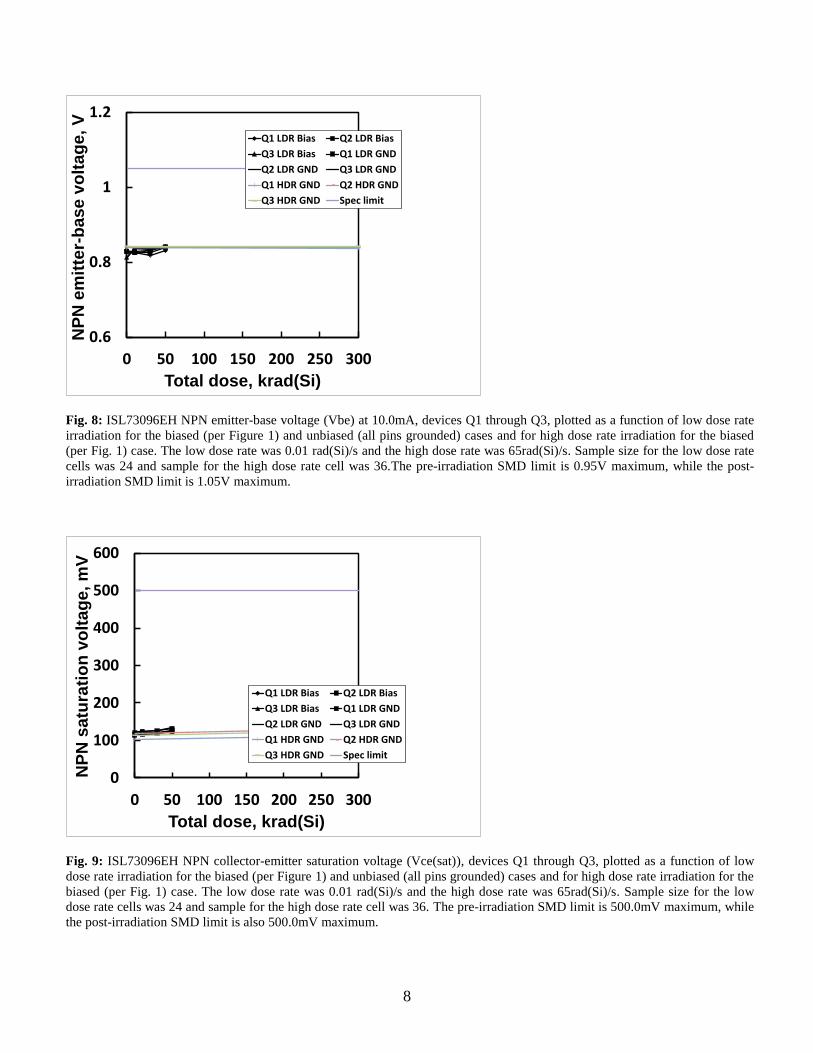
Fig. 8: ISL73096EH NPN emitter-base voltage (Vbe) at 10.0mA, devices Q1 through Q3, plotted as a function of low dose rate
irradiation for the biased (per Figure 1) and unbiased (all pins grounded) cases and for high dose rate irradiation for the biased
(per Fig. 1) case. The low dose rate was 0.01 rad(Si)/s and the high dose rate was 65rad(Si)/s. Sample size for the low dose rate
cells was 24 and sample for the high dose rate cell was 36.The pre-irradiation SMD limit is 0.95V maximum, while the post-
irradiation SMD limit is 1.05V maximum.
Fig. 9: ISL73096EH NPN collector-emitter saturation voltage (Vce(sat)), devices Q1 through Q3, plotted as a function of low
dose rate irradiation for the biased (per Figure 1) and unbiased (all pins grounded) cases and for high dose rate irradiation for the
biased (per Fig. 1) case. The low dose rate was 0.01 rad(Si)/s and the high dose rate was 65rad(Si)/s. Sample size for the low
dose rate cells was 24 and sample for the high dose rate cell was 36. The pre-irradiation SMD limit is 500.0mV maximum, while
the post-irradiation SMD limit is also 500.0mV maximum.
0.6
0.8
1
1.2
0 50 100 150 200 250 300
NP
N e
mit
ter-
base
vo
ltag
e, V
Total dose, krad(Si)
Q1 LDR Bias Q2 LDR Bias
Q3 LDR Bias Q1 LDR GND
Q2 LDR GND Q3 LDR GND
Q1 HDR GND Q2 HDR GND
Q3 HDR GND Spec limit
0
100
200
300
400
500
600
0 50 100 150 200 250 300
NP
N s
atu
rati
on
vo
ltag
e,
mV
Total dose, krad(Si)
Q1 LDR Bias Q2 LDR Bias
Q3 LDR Bias Q1 LDR GND
Q2 LDR GND Q3 LDR GND
Q1 HDR GND Q2 HDR GND
Q3 HDR GND Spec limit
9
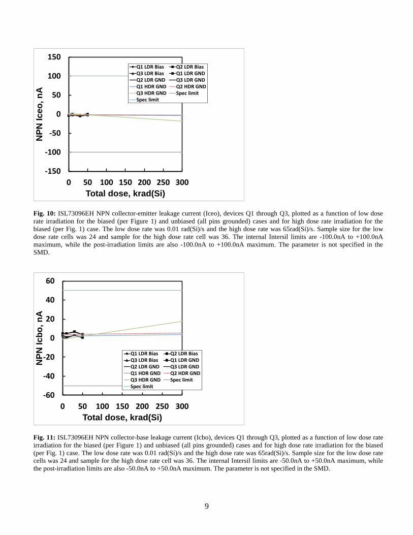
Fig. 10: ISL73096EH NPN collector-emitter leakage current (Iceo), devices Q1 through Q3, plotted as a function of low dose
rate irradiation for the biased (per Figure 1) and unbiased (all pins grounded) cases and for high dose rate irradiation for the
biased (per Fig. 1) case. The low dose rate was 0.01 rad(Si)/s and the high dose rate was 65rad(Si)/s. Sample size for the low
dose rate cells was 24 and sample for the high dose rate cell was 36. The internal Intersil limits are -100.0nA to +100.0nA
maximum, while the post-irradiation limits are also -100.0nA to +100.0nA maximum. The parameter is not specified in the
SMD.
Fig. 11: ISL73096EH NPN collector-base leakage current (Icbo), devices Q1 through Q3, plotted as a function of low dose rate
irradiation for the biased (per Figure 1) and unbiased (all pins grounded) cases and for high dose rate irradiation for the biased
(per Fig. 1) case. The low dose rate was 0.01 rad(Si)/s and the high dose rate was 65rad(Si)/s. Sample size for the low dose rate
cells was 24 and sample for the high dose rate cell was 36. The internal Intersil limits are -50.0nA to +50.0nA maximum, while
the post-irradiation limits are also -50.0nA to +50.0nA maximum. The parameter is not specified in the SMD.
-150
-100
-50
0
50
100
150
0 50 100 150 200 250 300
NP
N I
ce
o, n
A
Total dose, krad(Si)
Q1 LDR Bias Q2 LDR BiasQ3 LDR Bias Q1 LDR GNDQ2 LDR GND Q3 LDR GNDQ1 HDR GND Q2 HDR GNDQ3 HDR GND Spec limitSpec limit
-60
-40
-20
0
20
40
60
0 50 100 150 200 250 300
NP
N I
cb
o,
nA
Total dose, krad(Si)
Q1 LDR Bias Q2 LDR BiasQ3 LDR Bias Q1 LDR GNDQ2 LDR GND Q3 LDR GNDQ1 HDR GND Q2 HDR GNDQ3 HDR GND Spec limitSpec limit

10
Fig. 12: ISL73096EH PNP collector-base breakdown voltage (BVcbo), devices Q4 and Q5, plotted as a function of low dose
rate irradiation for the biased (per Figure 1) and unbiased (all pins grounded) cases and for high dose rate irradiation for the
biased (per Fig. 1) case. The low dose rate was 0.01 rad(Si)/s and the high dose rate was 65rad(Si)/s. Sample size for the low
dose rate cells was 24 and sample for the high dose rate cell was 36. The pre-irradiation SMD limit is -10.0V minimum, while
the post-irradiation SMD limit is also -10.0V minimum.
Fig. 13: ISL73096EH PNP collector-emitter breakdown voltage (BVceo), devices Q4 and Q5, plotted as a function of low dose
rate irradiation for the biased (per Figure 1) and unbiased (all pins grounded) cases and for high dose rate irradiation for the
biased (per Fig. 1) case. The low dose rate was 0.01 rad(Si)/s and the high dose rate was 65rad(Si)/s. Sample size for the low
dose rate cells was 24 and sample for the high dose rate cell was 36. The pre-irradiation SMD limit is -8.0V minimum, while the
post-irradiation SMD limit is also -8.0V minimum.
-30
-25
-20
-15
-10
-5
0 50 100 150 200 250 300
PN
P B
Vcb
o,
V
Total dose, krad(Si)
Q4 LDR Bias Q5 LDR Bias
Q4 LDR GND Q5 LDR GND
Q4 HDR GND Q5 HDR GND
Spec limit
-18
-16
-14
-12
-10
-8
-6
0 50 100 150 200 250 300
PN
P B
Vce
o,
V
Total dose, krad(Si)
Q4 LDR Bias Q5 LDR Bias
Q4 LDR GND Q5 LDR GND
Q4 HDR GND Q5 HDR GND
Spec limit

11
Fig. 14: ISL73096EH PNP collector-emitter breakdown voltage (BVces), devices Q4 and Q5, plotted as a function of low dose
rate irradiation for the biased (per Figure 1) and unbiased (all pins grounded) cases and for high dose rate irradiation for the
biased (per Fig. 1) case. The low dose rate was 0.01 rad(Si)/s and the high dose rate was 65rad(Si)/s. Sample size for the low
dose rate cells was 24 and sample for the high dose rate cell was 36. The pre-irradiation SMD limit is -10.0V minimum, while
the post-irradiation SMD limit is also -10.0V minimum.
Fig. 15: ISL73096EH PNP emitter-base breakdown voltage (BVebo), devices Q4 and Q5, plotted as a function of low dose rate
irradiation for the biased (per Figure 1) and unbiased (all pins grounded) cases and for high dose rate irradiation for the biased
(per Fig. 1) case. The low dose rate was 0.01 rad(Si)/s and the high dose rate was 65rad(Si)/s. Sample size for the low dose rate
cells was 24 and sample for the high dose rate cell was 36. The pre-irradiation SMD limit is -4.5V minimum, while the post-
irradiation SMD limit is also -4.5V minimum.
-30
-25
-20
-15
-10
-5
0 50 100 150 200 250 300
PN
P B
Vce
s
Total dose, krad(Si)
Q4 LDR Bias Q5 LDR Bias
Q4 LDR GND Q5 LDR GND
Q4 HDR GND Q5 HDR GND
Spec limit
-6
-5.5
-5
-4.5
-4
0 50 100 150 200 250 300
PN
P B
Veb
o,
V
Total dose, krad(Si)
Q4 LDR Bias Q5 LDR Bias
Q4 LDR GND Q5 LDR GND
Q4 HDR GND Q5 HDR GND
Spec limit

12
Fig. 16: ISL73096EH PNP common-emitter current gain (Hfe) at Ic = 10.0mA and Vce = 2.0V, devices Q4 and Q5, plotted as a
function of low dose rate irradiation for the biased (per Figure 1) and unbiased (all pins grounded) cases and for high dose rate
irradiation for the biased (per Fig. 1) case. The low dose rate was 0.01 rad(Si)/s and the high dose rate was 65rad(Si)/s. Sample
size for the low dose rate cells was 24 and sample for the high dose rate cell was 36. The pre-irradiation SMD limit is 40
minimum, while the post-irradiation SMD limit is 20 minimum. Current gain is a dimensionless parameter.
Fig. 17: ISL73096EH PNP Early voltage (VA), devices Q4 and Q5, plotted as a function of low dose rate irradiation for the
biased (per Figure 1) and unbiased (all pins grounded) cases and for high dose rate irradiation for the biased (per Fig. 1) case.
The low dose rate was 0.01 rad(Si)/s and the high dose rate was 65rad(Si)/s. Sample size for the low dose rate cells was 24 and
sample for the high dose rate cell was 36. The pre-irradiation SMD limit is 10.0V minimum, while the post-irradiation SMD
limit is also 10.0V minimum.
10
20
30
40
50
60
70
80
0 50 100 150 200 250 300
PN
P H
fe
Total dose, krad(Si)
Q4 LDR Bias Q5 LDR Bias
Q4 LDR GND Q5 LDR GND
Q4 HDR GND Q5 HDR GND
Spec limit
0
10
20
30
40
50
60
0 50 100 150 200 250 300
PN
P E
arl
y v
olt
ag
e,
V
Total dose, krad(Si)
Q4 LDR Bias Q5 LDR Bias
Q4 LDR GND Q5 LDR GND
Q4 HDR GND Q5 HDR GND
Spec limit

13
Fig. 18: ISL73096EH PNP emitter-base voltage (Vbe) at 10.0mA, devices Q4 and Q5, plotted as a function of low dose rate
irradiation for the biased (per Figure 1) and unbiased (all pins grounded) cases and for high dose rate irradiation for the biased
(per Fig. 1) case. The low dose rate was 0.01 rad(Si)/s and the high dose rate was 65rad(Si)/s. Sample size for the low dose rate
cells was 24 and sample for the high dose rate cell was 36. The pre-irradiation SMD limit is -0.95V maximum, while the post-
irradiation SMD limit is -1.05V maximum.
Fig. 19: ISL73096EH PNP collector-emitter saturation voltage (Vce(sat)), devices Q4 and Q5, plotted as a function of low dose
rate irradiation for the biased (per Figure 1) and unbiased (all pins grounded) cases and for high dose rate irradiation for the
biased (per Fig. 1) case. The low dose rate was 0.01 rad(Si)/s and the high dose rate was 65rad(Si)/s. Sample size for the low
dose rate cells was 24 and sample for the high dose rate cell was 36. The pre-irradiation SMD limit is -500.0mV maximum,
while the post-irradiation SMD limit is also -500.0mV maximum.
-1.2
-1
-0.8
-0.6
-0.4
0 50 100 150 200 250 300
PN
P e
mit
ter-
base
vo
ltag
e, V
Total dose, krad(Si)
Q4 LDR Bias Q5 LDR Bias
Q4 LDR GND Q5 LDR GND
Q4 HDR GND Q5 HDR GND
Spec limit
-600
-500
-400
-300
-200
-100
0
0 50 100 150 200 250 300
PN
P s
atu
rati
on
vo
ltag
e,
mV
Total dose, krad(Si)
Q4 LDR Bias Q5 LDR Bias
Q4 LDR GND Q5 LDR GND
Q4 HDR GND Q5 HDR GND
Spec limit

14
Fig. 20: ISL73096EH PNP collector-emitter leakage current (Iceo), devices Q4 and Q5, plotted as a function of low dose rate
irradiation for the biased (per Figure 1) and unbiased (all pins grounded) cases and for high dose rate irradiation for the biased
(per Fig. 1) case. The low dose rate was 0.01 rad(Si)/s and the high dose rate was 65rad(Si)/s. Sample size for the low dose rate
cells was 24 and sample for the high dose rate cell was 36. The internal Intersil limits are -100.0nA to +100.0nA maximum,
while the post-irradiation limits are also -100.0nA to +100.0nA maximum. The parameter is not specified in the SMD.
Fig. 21: ISL73096EH PNP collector-base leakage current (Icbo), devices Q4 and Q5, plotted as a function of low dose rate
irradiation for the biased (per Figure 1) and unbiased (all pins grounded) cases and for high dose rate irradiation for the biased
(per Fig. 1) case. The low dose rate was 0.01 rad(Si)/s and the high dose rate was 65rad(Si)/s. Sample size for the low dose rate
cells was 24 and sample for the high dose rate cell was 36. The internal Intersil limits are -30.0nA to +30.0nA maximum, while
the post-irradiation limits are also -30.0nA to +30.0nA maximum. The parameter is not specified in the SMD.
-150
-100
-50
0
50
100
150
0 50 100 150 200 250 300
PN
P I
ceo
, n
A
Total dose, krad(Si)
Q4 LDR Bias Q5 LDR Bias
Q4 LDR GND Q5 LDR GND
Q4 HDR GND Q5 HDR GND
Spec limit Spec limit
-40
-30
-20
-10
0
10
20
30
40
0 50 100 150 200 250 300
PN
P I
cb
o,
nA
Total dose, krad(Si)
Q4 LDR Bias Q5 LDR Bias
Q4 LDR GND Q5 LDR GND
Q4 HDR GND Q5 HDR GND
Spec limit Spec limit

15
6: Conclusion
This document reports results of low and high dose rate testing of the ISL73096EH NPN/PNP transistor array.
Parts were irradiated at 0.01 rad(Si)/s under biased and unbiased conditions and at 65rad(Si)/s under biased conditions
per MIL-STD-883 Test Method 1019.7. The low dose rate tests were run to 50 krad(Si) and the high dose rate test
was run to 300 krad(Si). All parameters showed excellent stability and remained within the pre- and post-irradiation
limits at all downpoints. No device sensitivity (meaning measurable differences in irradiation response between
transistors on the same die, the equivalent of channel sensitivity in for example multichannel operational amplifiers)
was noted at any of the downpoints. Similarly we saw no dose rate or bias sensitivity at all, and the part is not
considered to be low dose rate sensitive.
7: Appendices
7.1: Reported parameters and their post-radiation SMD limits.
Fig.
Type Parameter
Limit,
low
Limit,
high Units Notes
2
NPN Collector-base breakdown voltage 12.0 - V Emitter open, Ic = 100 µA
3 NPN Collector-emitter breakdown voltage 8.0 - V Base open, Ic = 100µA
4 NPN Collector-emitter breakdown voltage 10.0 - V Base tied to emitter, Ic = 100µA
5 NPN Emitter-base breakdown voltage 5.5 - V Ie = 10 µA
6 NPN Common-emitter current gain 40 - - Ic = 10 mA, Vce = 2.0 V
7 NPN Early voltage 20.0 - V Ic = 1 mA, Vce = 3.5 V
8 NPN Emitter-base voltage 1.05 - V Ie = 10.0 mA
9 NPN Collector-emitter saturation voltage 500.0 - mV Ic = 10 mA, Ib = 1 mA
10 NPN Collector-emitter leakage -100.0 +100.0 nA
11 NPN Collector-base leakage -50.0 +50.0 nA
12 PNP Collector-base breakdown voltage 10.0 - V Emitter open, Ic = 100 µA
13 PNP Collector-emitter breakdown voltage 8.0 - V Base open, Ic = 100µA
14 PNP Collector-emitter breakdown voltage 10.0 - V Base tied to emitter, Ic = 100µA
15 PNP Emitter-base breakdown voltage 4.5 - V Ie = 10 µA
16 PNP Common-emitter current gain 20 200 - Ic = 10 mA, Vce = 2.0 V
17 PNP Early voltage 10.0 - V Ic = 1 mA, Vce = 3.5 V
18 PNP Emitter-base voltage 1.05 - V Ie = 10.0 mA
19 PNP Collector-emitter saturation voltage 500.0 - mV Ic = 10 mA, Ib = 1 mA
20 PNP Collector-emitter leakage -100.0 +100.0 nA
21 PNP Collector-base leakage -30.0 +30.0 nA
8: Document revision history
Revision Date Pages Comments
0 29 May 2014 All Original issue


![마더세이프라운드 radiation dose[윤석남 교수]](https://static.fdocuments.net/doc/165x107/55637202d8b42a3b708b4b92/-radiation-dose-.jpg)