
ISL2110, ISL2111 Datasheet - Intersil · ISL2110, ISL2111 100V, 3A/4A Peak, High Frequency...
15
FN6295 Rev.7.00 Page 1 of 15 Mar 16, 2017 FN6295 Rev.7.00 Mar 16, 2017 ISL2110, ISL2111 100V, 3A/4A Peak, High Frequency Half-Bridge Drivers DATASHEET The ISL2110 , ISL2111 are 100V, high frequency, half-bridge N-Channel power MOSFET driver ICs. They are based on the popular HIP2100, HIP2101 half-bridge drivers, but offer several performance improvements. Peak output pull-up/pull-down current has been increased to 3A/4A, which significantly reduces switching power losses and eliminates the need for external totem-pole buffers in many applications. Also, the low end of the V DD operational supply range has been extended to 8VDC. The ISL2110 has additional input hysteresis for superior operation in noisy environments and the inputs of the ISL2111, like those of the ISL2110, can now safely swing to the V DD supply rail. Related Literature • For a full list of related documents, visit our website - ISL2110 , ISL2111 product pages Applications • Telecom half-bridge DC/DC converters • Telecom full-bridge DC/DC converters • Two-switch forward converters • Active-clamp forward converters • Class-D audio amplifiers Features • Drives N-Channel MOSFET half-bridge • SOIC, DFN, and TDFN package options • SOIC, DFN, and TDFN packages compliant with 100V conductor spacing guidelines per IPC-2221 • Pb-free (RoHS compliant) • Bootstrap supply max voltage to 114VDC • On-chip 1W bootstrap diode • Fast propagation times for multi-MHz circuits • Drives 1nF load with typical rise/fall times of 9ns/7.5ns • CMOS compatible input thresholds (ISL2110) • 3.3V/TTL compatible input thresholds (ISL2111) • Independent inputs provide flexibility • No start-up problems • Outputs unaffected by supply glitches, HS ringing below ground or HS slewing at high dv/dt • Low power consumption • Wide supply voltage range (8V to 14V) • Supply undervoltage protection • 1.6W/1W typical output pull-up/pull-down resistance FIGURE 1. APPLICATION BLOCK DIAGRAM SECONDARY CIRCUIT +100V CONTROL CONTROLLER PWM LI HI HO LO V DD HS HB +12V V SS REFERENCE AND ISOLATION DRIVE LO DRIVE HI ISL2110 ISL2111
Transcript of ISL2110, ISL2111 Datasheet - Intersil · ISL2110, ISL2111 100V, 3A/4A Peak, High Frequency...

FN6295Rev.7.00
Mar 16, 2017
ISL2110, ISL2111100V, 3A/4A Peak, High Frequency Half-Bridge Drivers
DATASHEET
The ISL2110, ISL2111 are 100V, high frequency, half-bridge N-Channel power MOSFET driver ICs. They are based on the popular HIP2100, HIP2101 half-bridge drivers, but offer several performance improvements. Peak output pull-up/pull-down current has been increased to 3A/4A, which significantly reduces switching power losses and eliminates the need for external totem-pole buffers in many applications. Also, the low end of the VDD operational supply range has been extended to 8VDC. The ISL2110 has additional input hysteresis for superior operation in noisy environments and the inputs of the ISL2111, like those of the ISL2110, can now safely swing to the VDD supply rail.
Related Literature• For a full list of related documents, visit our website
- ISL2110, ISL2111 product pages
Applications• Telecom half-bridge DC/DC converters
• Telecom full-bridge DC/DC converters
• Two-switch forward converters
• Active-clamp forward converters
• Class-D audio amplifiers
Features• Drives N-Channel MOSFET half-bridge
• SOIC, DFN, and TDFN package options
• SOIC, DFN, and TDFN packages compliant with 100V conductor spacing guidelines per IPC-2221
• Pb-free (RoHS compliant)
• Bootstrap supply max voltage to 114VDC
• On-chip 1W bootstrap diode
• Fast propagation times for multi-MHz circuits
• Drives 1nF load with typical rise/fall times of 9ns/7.5ns
• CMOS compatible input thresholds (ISL2110)
• 3.3V/TTL compatible input thresholds (ISL2111)
• Independent inputs provide flexibility
• No start-up problems
• Outputs unaffected by supply glitches, HS ringing below ground or HS slewing at high dv/dt
• Low power consumption
• Wide supply voltage range (8V to 14V)
• Supply undervoltage protection
• 1.6W/1W typical output pull-up/pull-down resistance
FIGURE 1. APPLICATION BLOCK DIAGRAM
SECONDARYCIRCUIT
+100V
CO
NT
RO
L
CONTROLLERPWM
LI
HI HO
LO
VDD
HS
HB
+12V
VSS
REFERENCEAND
ISOLATION
DRIVELO
DRIVEHI
ISL2110ISL2111
FN6295 Rev.7.00 Page 1 of 15Mar 16, 2017

ISL2110, ISL2111
Functional Block Diagram
FIGURE 2. FUNCTIONAL BLOCK DIAGRAM
UNDERVOLTAGE
VDD
HI
LI
VSS
DRIVER
DRIVER
HB
HO
HS
LO
LEVEL SHIFT
UNDERVOLTAGE
EPAD (DFN Package Only)
ISL2111
ISL2111
*EPAD = Exposed Pad. The EPAD is electrically isolated from all other pins. For best thermal performance, connect the EPAD to the PCB power ground plane.
FN6295 Rev.7.00 Page 2 of 15Mar 16, 2017

ISL2110, ISL2111
Application Diagrams
Ordering Information
PART NUMBER(Notes 3, 4)
PARTMARKING
TEMPRANGE
(°C)PACKAGE
(RoHS COMPLIANT)PKG.
DWG. #
ISL2110ABZ (Note 1) 2110 ABZ -40 to +125 8 Ld SOIC M8.15
ISL2110AR4Z (Note 2) 211 0AR4Z -40 to +125 12 Ld 4x4 DFN L12.4x4A
ISL2111ABZ (Note 1) 2111 ABZ -40 to +125 8 Ld SOIC M8.15
ISL2111AR4Z (Note 2) 211 1AR4Z -40 to +125 12 Ld 4x4 DFN L12.4x4A
ISL2111ARTZ (Note 2) 211 1ARTZ -40 to +125 10 Ld 4x4 TDFN L10.4x4
ISL2111BR4Z (Note 2) 211 1BR4Z -40 to +125 8 Ld 4x4 DFN L8.4x4
NOTES:
1. Add “-T” for 2.5k unit tape and reel options. Refer to TB347 for details on reel specifications.
2. Add “-T” suffix for 6k unit tape and reel options. Refer to TB347 for details on reel specifications.
3. These Intersil Pb-free plastic packaged products employ special Pb-free material sets, molding compounds/die attach materials, and 100% matte tin plate plus anneal (e3 termination finish, which is RoHS compliant and compatible with both SnPb and Pb-free soldering operations). Intersil Pb-free products are MSL classified at Pb-free peak reflow temperatures that meet or exceed the Pb-free requirements of IPC/JEDEC J STD-020.
4. For Moisture Sensitivity Level (MSL), please see device information page for ISL2110, ISL2111. For more information on MSL, see Tech Brief TB363.
SECONDARY
ISOLATION
PWM
+48V
+12V
CIRCUIT
FIGURE 3. TWO-SWITCH FORWARD CONVERTER
ISL2110ISL2111
SECONDARYCIRCUIT
ISOLATION
PWM
+48V
+12V
FIGURE 4. FORWARD CONVERTER WITH AN ACTIVE-CLAMP
ISL2110ISL2111
FN6295 Rev.7.00 Page 3 of 15Mar 16, 2017

ISL2110, ISL2111
Pin ConfigurationsISL2111ARTZ
(10 LD 4x4 TDFN)TOP VIEW
ISL2110AR4Z, ISL2111AR4Z(12 LD 4x4 DFN)
TOP VIEW
ISL2110ABZ, ISL2111ABZ(8 LD SOIC)
TOP VIEW
ISL2111BR4Z(8 LD 4x4 DFN)
TOP VIEW
2
3
4
1
5
9
8
7
10
6
VDD
HB
HO
HS
NC
LO
VSS
LI
HI
NC
VDD
NC
NC
HB
HO
LO
VSS
NC
NC
LI
HS HI
2
3
4
1
5
11
10
9
12
8
6 7
EPAD*
*EPAD = EXPOSED PAD
5
6
8
7
4
3
2
1VDD
HB
HO
HS
LO
LI
HI
VSS2
3
4
1
7
6
5
8VDD
HB
HO
HS
LO
VSS
LI
HIEPAD*
*EPAD = EXPOSED PAD
Pin DescriptionsSYMBOL DESCRIPTION
VDD Positive supply to lower gate driver. Bypass this pin to VSS.
HB High-side bootstrap supply. External bootstrap capacitor is required. Connect positive side of bootstrap capacitor to this pin. Bootstrap diode is on-chip.
HO High-side output. Connect to gate of high-side power MOSFET.
HS High-side source connection. Connect to source of high-side power MOSFET. Connect negative side of bootstrap capacitor to this pin.
HI High-side input
LI Low-side input
VSS Chip negative supply, which will generally be ground.
LO Low-side output. Connect to gate of low-side power MOSFET.
NC No connect
EPAD Exposed pad. Connect to ground or float. The EPAD is electrically isolated from all other pins.
FN6295 Rev.7.00 Page 4 of 15Mar 16, 2017

ISL2110, ISL2111
Absolute Maximum Ratings Thermal InformationSupply Voltage, VDD, VHB - VHS (Notes 5, 6) . . . . . . . . . . . . . . . 0.3V to 18VLI and HI Voltages (Note 6) . . . . . . . . . . . . . . . . . . . . . . . -0.3V to VDD + 0.3VVoltage on LO (Note 6) . . . . . . . . . . . . . . . . . . . . . . . . . . . -0.3V to VDD + 0.3VVoltage on HO (Note 6) . . . . . . . . . . . . . . . . . . . . . .VHS - 0.3V to VHB + 0.3VVoltage on HS (Continuous) (Note 6) . . . . . . . . . . . . . . . . . . . . . -1V to 110VVoltage on HB (Note 6). . . . . . . . . . . . . . . . . . . . . . . . . . . . . . . . . . . . . . . 118VAverage Current in VDD to HB Diode . . . . . . . . . . . . . . . . . . . . . . . . . 100mA
Maximum Recommended Operating ConditionsSupply Voltage, VDD . . . . . . . . . . . . . . . . . . . . . . . . . . . . . . . . . . . . . 8V to 14VVoltage on HS . . . . . . . . . . . . . . . . . . . . . . . . . . . . . . . . . . . . . . . . -1V to 100VVoltage on HS . . . . . . . . . . . . . . . . . . . . . .(Repetitive Transient) -5V to 105VVoltage on HB . . . . . . . . . . .VHS+7V to VHS+14V and VDD - 1V to VDD+100VHS Slew Rate. . . . . . . . . . . . . . . . . . . . . . . . . . . . . . . . . . . . . . . . . . . . <50V/ns
Thermal Resistance (Typical) JA (°C/W) JC (°C/W)8 Ld SOIC (Notes 7, 10) . . . . . . . . . . . . . . . . 95 4610 Ld TDFN (Notes 8, 9) . . . . . . . . . . . . . . . 40 2.512 Ld DFN (Notes 8, 9) . . . . . . . . . . . . . . . . 39 2.58 Ld DFN (Notes 8, 9). . . . . . . . . . . . . . . . . . 40 4.0
Max Power Dissipation at +25°C in Free Air8 Ld SOIC (Notes 7, 10) . . . . . . . . . . . . . . . . . . . . . . . . . . . . . . . . . . . . . . 1.3W10 Ld TDFN (Notes 8, 9) . . . . . . . . . . . . . . . . . . . . . . . . . . . . . . . . . . . . . 3.0W12 Ld DFN (Notes 8, 9) . . . . . . . . . . . . . . . . . . . . . . . . . . . . . . . . . . . . . . 3.1W8 Ld DFN (Notes 8, 9) . . . . . . . . . . . . . . . . . . . . . . . . . . . . . . . . . . . . . . 3.1W
Storage Temperature Range. . . . . . . . . . . . . . . . . . . . . . . .-65°C to +150°CJunction Temperature Range . . . . . . . . . . . . . . . . . . . . . . .-55°C to +150°CPb-Free Reflow Profile . . . . . . . . . . . . . . . . . . . . . . . . . . . . . . . . . . see TB493
CAUTION: Do not operate at or near the maximum ratings listed for extended periods of time. Exposure to such conditions may adversely impact product reliability andresult in failures not covered by warranty.
NOTES:
5. The ISL2110 and ISL2111 are capable of derated operation at supply voltages exceeding 14V. Figure 24 shows the high-side voltage derating curve for this mode of operation.
6. All voltages referenced to VSS unless otherwise specified.
7. JA is measured with the component mounted on a high-effective thermal conductivity test board in free air. See Tech Brief TB379 for details.
8. JA is measured in free air with the component mounted on a high-effective thermal conductivity test board with “direct attach” features. See Tech Brief TB379.
9. For JC, the “case temp” location is the center of the exposed metal pad on the package underside.
10. For JC, the “case temp” location is taken at the package top center.
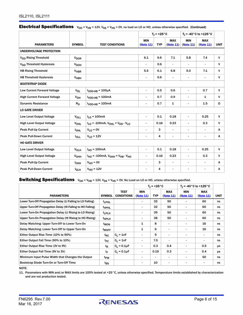
Electrical Specifications VDD = VHB = 12V, VSS = VHS = 0V, no load on LO or HO, unless otherwise specified.
PARAMETERS SYMBOL TEST CONDITIONS
TJ = +25°C TJ = -40°C to +125°C
UNITMIN
(Note 11) TYPMAX
(Note 11)MIN
(Note 11)MAX
(Note 11)
SUPPLY CURRENTS
VDD Quiescent Current IDD ISL2110; LI = HI = 0V - 0.10 0.25 - 0.30 mA
VDD Quiescent Current IDD ISL2111; LI = HI = 0V - 0.30 0.45 - 0.55 mA
VDD Operating Current IDDO ISL2110; f = 500kHz - 3.4 5.0 - 5.5 mA
VDD Operating Current IDDO ISL2111; f = 500kHz - 3.5 5.0 - 5.5 mA
Total HB Quiescent Current IHB LI = HI = 0V - 0.10 0.15 - 0.20 mA
Total HB Operating Current IHBO f = 500kHz - 3.4 5.0 - 5.5 mA
HB to VSS Current, Quiescent IHBS LI = HI = 0V; VHB = VHS = 114V - 0.05 1.50 - 10 µA
HB to VSS Current, Operating IHBSO f = 500kHz; VHB = VHS = 114V - 1.2 - - - mA
INPUT PINS
Low Level Input Voltage Threshold VIL ISL2110 3.7 4.4 - 3.5 - V
Low Level Input Voltage Threshold VIL ISL2111 1.4 1.8 - 1.2 - V
High Level Input Voltage Threshold VIH ISL2110 - 6.6 7.4 - 7.6 V
High Level Input Voltage Threshold VIH ISL2111 - 1.8 2.2 - 2.4 V
Input Voltage Hysteresis VIHYS ISL2110 - 2.2 - - - V
Input Pull-Down Resistance RI - 210 - 100 500 kΩ
FN6295 Rev.7.00 Page 5 of 15Mar 16, 2017
ISL2110, ISL2111
UNDERVOLTAGE PROTECTION
VDD Rising Threshold VDDR 6.1 6.6 7.1 5.8 7.4 V
VDD Threshold Hysteresis VDDH - 0.6 - - - V
HB Rising Threshold VHBR 5.5 6.1 6.8 5.0 7.1 V
HB Threshold Hysteresis VHBH - 0.6 - - - V
BOOTSTRAP DIODE
Low Current Forward Voltage VDL IVDD-HB = 100µA - 0.5 0.6 - 0.7 V
High Current Forward Voltage VDH IVDD-HB = 100mA - 0.7 0.9 - 1 V
Dynamic Resistance RD IVDD-HB = 100mA - 0.7 1 - 1.5 Ω
LO GATE DRIVER
Low Level Output Voltage VOLL ILO = 100mA - 0.1 0.18 - 0.25 V
High Level Output Voltage VOHL ILO = -100mA, VOHL = VDD - VLO - 0.16 0.23 - 0.3 V
Peak Pull-Up Current IOHL VLO = 0V - 3 - - - A
Peak Pull-Down Current IOLL VLO = 12V - 4 - - - A
HO GATE DRIVER
Low Level Output Voltage VOLH IHO = 100mA - 0.1 0.18 - 0.25 V
High Level Output Voltage VOHH IHO = -100mA, VOHH = VHB - VHO - 0.16 0.23 - 0.3 V
Peak Pull-Up Current IOHH VHO = 0V - 3 - - - A
Peak Pull-Down Current IOLH VHO = 12V - 4 - - - A
Electrical Specifications VDD = VHB = 12V, VSS = VHS = 0V, no load on LO or HO, unless otherwise specified. (Continued)
PARAMETERS SYMBOL TEST CONDITIONS
TJ = +25°C TJ = -40°C to +125°C
UNITMIN
(Note 11) TYPMAX
(Note 11)MIN
(Note 11)MAX
(Note 11)
Switching Specifications VDD = VHB = 12V, VSS = VHS = 0V, No Load on LO or HO, unless otherwise specified.
PARAMETERS SYMBOLTEST
CONDITIONS
TJ = +25°C TJ = -40°C to +125°C
UNITMIN
(Note 11) TYPMAX
(Note 11)MIN
(Note 11)MAX
(Note 11)
Lower Turn-Off Propagation Delay (LI Falling to LO Falling) tLPHL - 32 50 - 60 ns
Upper Turn-Off Propagation Delay (HI Falling to HO Falling) tHPHL - 32 50 - 60 ns
Lower Turn-On Propagation Delay (LI Rising to LO Rising) tLPLH - 39 50 - 60 ns
Upper Turn-On Propagation Delay (HI Rising to HO Rising) tHPLH - 38 50 - 60 ns
Delay Matching: Upper Turn-Off to Lower Turn-On tMON 1 8 - - 16 ns
Delay Matching: Lower Turn-Off to Upper Turn-On tMOFF 1 6 - - 16 ns
Either Output Rise Time (10% to 90%) tRC CL = 1nF - 9 - - - ns
Either Output Fall Time (90% to 10%) tFC CL = 1nF - 7.5 - - - ns
Either Output Rise Time (3V to 9V) tR CL = 0.1µF - 0.3 0.4 - 0.5 µs
Either Output Fall Time (9V to 3V) tF CL = 0.1µF - 0.19 0.3 - 0.4 µs
Minimum Input Pulse Width that Changes the Output tPW - - - - 50 ns
Bootstrap Diode Turn-On or Turn-Off Time tBS - 10 - - - ns
NOTE:11. Parameters with MIN and/or MAX limits are 100% tested at +25°C, unless otherwise specified. Temperature limits established by characterization
and are not production tested.
FN6295 Rev.7.00 Page 6 of 15Mar 16, 2017

ISL2110, ISL2111
Timing Diagrams
FIGURE 5. PROPAGATION DELAYS FIGURE 6. DELAY MATCHING
tHPLH,tLPLH
tHPHL,tLPHL
HI, LI
HO, LOtMON tMOFF
LI
HI
LO
HO
FN6295 Rev.7.00 Page 7 of 15Mar 16, 2017

ISL2110, ISL2111
Typical Performance Curves
FIGURE 7. ISL2110 IDD OPERATING CURRENT vs FREQUENCY FIGURE 8. ISL2111 IDD OPERATING CURRENT vs FREQUENCY
FIGURE 9. IHB OPERATING CURRENT vs FREQUENCY FIGURE 10. IHBS OPERATING CURRENT vs FREQUENCY
FIGURE 11. HIGH LEVEL OUTPUT VOLTAGE vs TEMPERATURE FIGURE 12. LOW LEVEL OUTPUT VOLTAGE vs TEMPERATURE
0.1
1.0
10.0
FREQUENCY (Hz)
I DD
O (
mA
)
T = +25°C
T = -40°C
T = +125°C
T = +150°C
10k 100k 1.103k 10k 100k 1.103k0.1
1.0
10.0
FREQUENCY (Hz)
I DD
O (
mA
) T = +25°C
T = -40°C
T = +150°C
T = +125°C
FREQUENCY (Hz)
I HB
O (
mA
)
0.01
1.0
10.0
T = +25°C
T = -40°C
T = +125°C
T = +150°C
10k 100k 1.103k
0.1
FREQUENCY (Hz)
I HB
SO
(m
A)
0.01
1.0
10.0
T = -40°C
T = +125°C
T = +150°C
10k 100k 1.103k
0.1T = +25°C
-50 0 50 100 15050
100
150
200
250
300
TEMPERATURE (°C)
VO
HL, V
OH
H (
mV
)
VDD = VHB = 12V
VDD = VHB = 14V
VDD = VHB = 8V
-50 0 50 100 15050
100
150
200
VO
LL, V
OL
H (
mV
)
TEMPERATURE (°C)
VDD = VHB = 12V
VDD = VHB = 14V
VDD = VHB = 8V
FN6295 Rev.7.00 Page 8 of 15Mar 16, 2017

ISL2110, ISL2111
FIGURE 13. UNDERVOLTAGE LOCKOUT THRESHOLD vs TEMPERATURE
FIGURE 14. UNDERVOLTAGE LOCKOUT HYSTERESIS vs TEMPERATURE
FIGURE 15. ISL2110 PROPAGATION DELAYS vs TEMPERATURE FIGURE 16. ISL2111 PROPAGATION DELAYS vs TEMPERATURE
FIGURE 17. ISL2110 DELAY MATCHING vs TEMPERATURE FIGURE 18. ISL2111 DELAY MATCHING vs TEMPERATURE
Typical Performance Curves (Continued)
VD
DR
, VH
BR
(V
)
-50 0 50 100 150
6.7
TEMPERATURE (°C)
VHBR
VDDR
6.5
6.3
6.1
5.9
5.7
5.5
5.3
VD
DH
, VH
BH
(V
)
-50 0 50 100 150
0.70
TEMPERATURE (°C)
VHBH
VDDH
0.65
0.60
0.55
0.50
0.45
0.40
25
30
35
40
45
50
55
t LP
LH
, tL
PH
L, t
HP
LH
, tH
PH
L (
ns)
-50 0 50 100 150
TEMPERATURE (°C)
tLPHL
tHPHL
tLPLH
tHPLH
25
30
35
40
45
50
55
t LP
LH
, tL
PH
L, t
HP
LH
, tH
PH
L (
ns)
-50 0 50 100 150
TEMPERATURE (°C)
tLPHL
tHPHL
tLPLH
tHPLH
4.0
4.5
5.0
5.5
6.0
6.5
7.0
7.5
8.0
t MO
N, t
MO
FF (
ns)
-50 0 50 100 150
TEMPERATURE (°C)
tMOFF
tMON
4.04.55.05.56.06.57.07.58.08.59.09.5
10.0
t MO
N, t
MO
FF (
ns)
-50 0 50 100 150
TEMPERATURE (°C)
tMOFF
tMON
FN6295 Rev.7.00 Page 9 of 15Mar 16, 2017

ISL2110, ISL2111
FIGURE 19. PEAK PULL-UP CURRENT vs OUTPUT VOLTAGE FIGURE 20. PEAK PULL-DOWN CURRENT vs OUTPUT VOLTAGE
FIGURE 21. ISL2110 QUIESCENT CURRENT vs VOLTAGE FIGURE 22. ISL2111 QUIESCENT CURRENT vs VOLTAGE
FIGURE 23. BOOTSTRAP DIODE I-V CHARACTERISTICS FIGURE 24. VHS VOLTAGE vs VDD VOLTAGE
Typical Performance Curves (Continued)
0 4 8 10 120
0.5
1.0
1.5
2.0
2.5
3.0
3.5
VLO, VHO (V)
I OH
L, I
OH
H (
A)
2 6 0 4 8 10 120
1.5
2.0
2.5
3.0
3.5
4.0
4.5
VLO, VHO (V)
I OH
L, I
OH
H (
A)
2 6
1.0
0.5
0 5 10 15 200
102030405060708090
100110120
VDD, VHB (V)
I DD
, IH
B (
µA
)
IHB
IDD
0 5 10 15 20VDD, VHB (V)
I DD
, IH
B (
µA
)
020406080
100120140160180200220240260280300320
IHB
IDD
0.3 0.4 0.5 0.6 0.7 0.8
1.10-3
0.01
0.10
1.00
FORWARD VOLTAGE (V)
FO
RW
AR
D C
UR
RE
NT
(A
)
1.10-4
1.10-5
1.10-612 13 14 15 16
0
20
40
60
80
100
120
VH
S T
O V
SS
VO
LT
AG
E (
V)
VDD TO VSS VOLTAGE (V)
FN6295 Rev.7.00 Page 10 of 15Mar 16, 2017

ISL2110, ISL2111
Intersil products are manufactured, assembled and tested utilizing ISO9001 quality systems as notedin the quality certifications found at www.intersil.com/en/support/qualandreliability.html
Intersil products are sold by description only. Intersil may modify the circuit design and/or specifications of products at any time without notice, provided that such modification does not, in Intersil's sole judgment, affect the form, fit or function of the product. Accordingly, the reader is cautioned to verify that datasheets are current before placing orders. Information furnished by Intersil is believed to be accurate and reliable. However, no responsibility is assumed by Intersil or its subsidiaries for its use; nor for any infringements of patents or other rights of third parties which may result from its use. No license is granted by implication or otherwise under any patent or patent rights of Intersil or its subsidiaries.
For information regarding Intersil Corporation and its products, see www.intersil.com
For additional products, see www.intersil.com/en/products.html
© Copyright Intersil Americas LLC 2006-2017. All Rights Reserved.All trademarks and registered trademarks are the property of their respective owners.
About IntersilIntersil Corporation is a leading provider of innovative power management and precision analog solutions. The company's products address some of the largest markets within the industrial and infrastructure, mobile computing, and high-end consumer markets.
For the most updated datasheet, application notes, related documentation, and related parts, see the respective product information page found at www.intersil.com.
For a listing of definitions and abbreviations of common terms used in our documents, visit: www.intersil.com/glossary.
You may report errors or suggestions for improving this datasheet by visiting www.intersil.com/ask.
Reliability reports are also available from our website at www.intersil.com/support.
Revision History The revision history provided is for informational purposes only and is believed to be accurate, but not warranted. Please visit our website to make sure you have the latest revision.
DATE REVISION CHANGE
Mar 16, 2017 FN6295.7 Corrected the branding of FG ISL2111BR4Z in the order information table from "211 1BR4A" to "211 1BR4Z".Added Revision History table and About Intersil information.
Updated L10.4x4 Package Outline Drawing from Rev 1 to Rev 2. Change since Rev 1 is:“Tiebar note update from ‘Tiebar shown (if present) is a non-functional feature’ to ‘Tiebar shown (if present) is a non-functional feature and may be located on any of the 4 sides (or ends)’”.
Updated L12.4x4A Package Outline Drawing from Rev 1 to Rev 3. Changes since Rev 1 are:“Tiebar note update from ‘Tiebar shown (if present) is a non-functional feature’ to ‘Tiebar shown (if present) is a non-functional feature and may be located on any of the 4 sides (or ends)’”; “Bottom View changed from ‘3.2 REF’ TO ‘2.5 REF’"; “Typical Recommended Land Pattern changed from ‘3.80’ to ‘3.75’"; “Updated to new POD format by removing table listing dimensions and moving dimensions onto drawing”, and “Added typical recommended land pattern”.
Updated M8.15 Package Outline Drawing from Rev 3 to Rev 4. Change since Rev 3 is:“Changed Note 1 from 1982 to 1994“.
Updated L8.4x4 Package Outline Drawing from Rev 0 to Rev 1. Change since Rev 0 is:“Tiebar note update from ‘Tiebar shown (if present) is a non-functional feature’ to ‘Tiebar shown (if present) is a non-functional feature and may be located on any of the 4 sides (or ends)’”.
FN6295 Rev.7.00 Page 11 of 15Mar 16, 2017

ISL2110, ISL2111
FN6295 Rev.7.00 Page 12 of 15Mar 16, 2017
Package Outline DrawingL10.4x410 LEAD THIN DUAL FLAT NO-LEAD PLASTIC PACKAGE
Rev 2, 4/15
TYPICAL RECOMMENDED LAND PATTERNDETAIL "X"
SIDE VIEW
TOP VIEW
BOTTOM VIEW
located within the zone indicated. The pin #1 identifier may be
Unless otherwise specified, tolerance : Decimal ± 0.05
The configuration of the pin #1 identifier is optional, but must be
between 0.15mm and 0.30mm from the terminal tip.Dimension b applies to the metallized terminal and is measured
Dimensions in ( ) for Reference Only.
Dimensioning and tolerancing conform to AMSE Y14.5m-1994.
6.
either a mold or mark feature.
3.
5.
4.
2.
Dimensions are in millimeters.1.
NOTES:
4.00 2.60
0.15
(3.80)
(4X)
(10X 0.30)(8X 0.8)
0 .75
BASE PLANE
CSEATING PLANE
0.08
C0.10C
10 X 0.30
SEE DETAIL "X"
0.10
4
C AM B
INDEX AREA
6
PIN 1
4.00A
B
PIN #1 INDEX AREA
BSC
3.2 REF
8X 0.806
(10 X 0.60)
0 . 00 MIN.0 . 05 MAX.
C
0 . 2 REF
10X 0 . 40
3.00
(2.60)
( 3.00 )
0.05 M C
6
5
10
1
Tiebar shown (if present) is a non-functional feature and maybe located on any of the 4 sides (or ends).
For the most recent package outline drawing, see L10.4x4.

ISL2110, ISL2111
FN6295 Rev.7.00 Page 13 of 15Mar 16, 2017
Package Outline DrawingL12.4x4A12 LEAD DUAL FLAT NO-LEAD PLASTIC PACKAGE
Rev 3, 3/15
TYPICAL RECOMMENDED LAND PATTERNDETAIL "X"
SIDE VIEW
TOP VIEW
BOTTOM VIEW
located within the zone indicated. The pin #1 identifier may be
Unless otherwise specified, tolerance : Decimal ± 0.05
The configuration of the pin #1 identifier is optional, but must be
between 0.15mm and 0.30mm from the terminal tip.
Lead width applies to the metallized terminal and is measured
Dimensions in ( ) for Reference Only.
Dimensioning and tolerancing conform to AMSE Y14.5m-1994.
6.
either a mold or mark feature.
3.
5.
4.
2.
Dimensions are in millimeters.1.
NOTES:
4.00 1.58
0.15
( 3.75)
(4X)
( 12X 0 . 25)( 10X 0 . 5 )
1.00 MAX
BASE PLANE
CSEATING PLANE
0.08
C0.10C
12 X 0.25
SEE DETAIL "X"
0.10
4
C AM B
INDEX AREA
6
PIN 1
4.00A
B
PIN #1 INDEX AREA
2.5 REF
10X 0.50 BSC
6
( 12 X 0.65 )
0 . 00 MIN.0 . 05 MAX.
C
0 . 2 REF
12X 0 . 45
2.80
( 1.58)
( 2.80 )
0.05 M C
7
6
12
1
Tiebar shown (if present) is a non-functional feature and maybe located on any of the 4 sides (or ends).
For the most recent package outline drawing, see L12.4x4A.

ISL2110, ISL2111
FN6295 Rev.7.00 Page 14 of 15Mar 16, 2017
Package Outline DrawingM8.158 LEAD NARROW BODY SMALL OUTLINE PLASTIC PACKAGE
Rev 4, 1/12
DETAIL "A"
TOP VIEW
INDEX
AREA
1 2 3
-C-
SEATING PLANE
x 45°
NOTES:1. Dimensioning and tolerancing per ANSI Y14.5M-1994.2. Package length does not include mold flash, protrusions or gate burrs.
Mold flash, protrusion and gate burrs shall not exceed 0.15mm (0.006inch) per side.
3. Package width does not include interlead flash or protrusions. Interlead flash and protrusions shall not exceed 0.25mm (0.010 inch) per side.
4. The chamfer on the body is optional. If it is not present, a visual indexfeature must be located within the crosshatched area.
5. Terminal numbers are shown for reference only.6. The lead width as measured 0.36mm (0.014 inch) or greater above the
seating plane, shall not exceed a maximum value of 0.61mm (0.024 inch).7. Controlling dimension: MILLIMETER. Converted inch dimensions are not
necessarily exact.8. This outline conforms to JEDEC publication MS-012-AA ISSUE C.
SIDE VIEW “A
SIDE VIEW “B”
1.27 (0.050)
6.20 (0.244)5.80 (0.228)
4.00 (0.157)3.80 (0.150)
0.50 (0.20)0.25 (0.01)
5.00 (0.197)4.80 (0.189)
1.75 (0.069)1.35 (0.053)
0.25(0.010)0.10(0.004)
0.51(0.020)0.33(0.013)
8°0°
0.25 (0.010)0.19 (0.008)
1.27 (0.050)
0.40 (0.016)
1.27 (0.050)
5.20(0.205)
1
2
3
4 5
6
7
8
TYPICAL RECOMMENDED LAND PATTERN
2.20 (0.087)
0.60 (0.023)
For the most recent package outline drawing, see M8.15.

ISL2110, ISL2111
FN6295 Rev.7.00 Page 15 of 15Mar 16, 2017
Package Outline DrawingL8.4x48 LEAD DUAL FLAT NO-LEAD PLASTIC PACKAGE
Rev 1, 03/15
TYPICAL RECOMMENDED LAND PATTERNDETAIL "X"
SIDE VIEW
TOP VIEW
BOTTOM VIEW
located within the zone indicated. The pin #1 identifier may be
Unless otherwise specified, tolerance : Decimal ± 0.05
The configuration of the pin #1 identifier is optional, but must be
between 0.15mm and 0.30mm from the terminal tip.
Dimension applies to the metallized terminal and is measured
Dimensions in ( ) for Reference Only.
Dimensioning and tolerancing conform to ASME Y14.5m-1994.
6.
either a mold or mark feature.
3.
5.
4.
2.
Dimensions are in millimeters.1.
NOTES:
4.00 2.50 ± 0.10
0.15
( 3.80)
(4X)
( 8X 0 . 30 )( 6X 0 . 8 )
0 .9 ± 0.10
BASE PLANE
CSEATING PLANE
0.08
C0.10C
8 X 0.30
SEE DETAIL "X"
0.10
4
C AM B
INDEX AREA
6
PIN 1
4.00A
B
PIN #1 INDEX AREA
BSC
2.4 REF
6X 0.806
( 8 X 0.60 )
8X 0 . 40 ± 0.10
3.45 ± 0.10
( 2.50)
( 3.45 )
0.05 M C
5
4
8
1
0 . 00 MIN.0 . 05 MAX.
C
0 . 2 REF
Tiebar shown (if present) is a non-functional feature and maybe located on any of the 4 sides (or ends).
For the most recent package outline drawing, see L8.4x4.


