ISIM: The Simulator for The Impulse Adaptable …ISIM: The Simulator for The Impulse Adaptable...
48
ISIM: The Simulator for The Impulse Adaptable Memory System Lixin Zhang UUCS-99-017 Department of Computer Science University of Utah Salt Lake City, UT 84112, USA September 18, 1998 Abstract This document describes ISIM, the simulator for the Impulse Adaptable Memory System. Impulse adds two new features to a conventional memory system. First, it supports a configurable, extra level of address remapping at the memory controller. Second, it supports prefetching at the memory controller. Consequently, two new units, a remapping controller and a memory controller cache, are added to a traditional memory system to support the new Impulse features. ISIM is based on Paint, a PA-RISC instruction set interpreter. ISIM extends Paint with a detailed Impulse memory system model which includes a primary data cache, a secondary data cache, a system bus, an Impulse memory controller, and a renovated DRAM backend. Note that this document focuses on the Impulse extensions only. The reader should consult the Paint technical report [2] for an overview of the Paint simulation environment and terminology. This effort was sponsored in part by the Defense Advanced Research Projects Agency (DARPA)and the Air Force Research Laboratory (AFRL) under agreement number F30602-98-1-0101 and DARPA Order Numbers F393/00-01 and F376/00. The views and conclusions contained herein are those of the authors and should not be interpreted as necessarily representing the official polices or endorsements, either express or implied, of DARPA, AFRL, or the US Government.
Transcript of ISIM: The Simulator for The Impulse Adaptable …ISIM: The Simulator for The Impulse Adaptable...

ISIM: The Simulator for The ImpulseAdaptable Memory System
Lixin Zhang
UUCS-99-017
Department of Computer ScienceUniversity of Utah
Salt Lake City, UT 84112, USA
September 18, 1998
Abstract
This document describes ISIM, the simulator for the Impulse Adaptable Memory System. Impulseadds two new features to a conventional memory system. First, it supports a configurable, extralevel of address remapping at the memory controller. Second, it supports prefetching at the memorycontroller. Consequently, two new units, a remapping controller and a memory controller cache, areadded to a traditional memory system to support the new Impulse features. ISIM is based on Paint,a PA-RISC instruction set interpreter. ISIM extends Paint with a detailed Impulse memory systemmodel which includes a primary data cache, a secondary data cache, a system bus, an Impulsememory controller, and a renovated DRAM backend.
Note that this document focuses on the Impulse extensions only. The reader should consult the Painttechnical report [2] for an overview of the Paint simulation environment and terminology.
This effort was sponsored in part by the Defense Advanced Research Projects Agency (DARPA) and the Air ForceResearch Laboratory (AFRL) under agreement number F30602-98-1-0101 and DARPA Order Numbers F393/00-01 andF376/00. The views and conclusions contained herein are those of the authors and should not be interpreted as necessarilyrepresenting the official polices or endorsements, either express or implied, of DARPA, AFRL, or the US Government.

Report Documentation Page Form ApprovedOMB No. 0704-0188
Public reporting burden for the collection of information is estimated to average 1 hour per response, including the time for reviewing instructions, searching existing data sources, gathering andmaintaining the data needed, and completing and reviewing the collection of information. Send comments regarding this burden estimate or any other aspect of this collection of information,including suggestions for reducing this burden, to Washington Headquarters Services, Directorate for Information Operations and Reports, 1215 Jefferson Davis Highway, Suite 1204, ArlingtonVA 22202-4302. Respondents should be aware that notwithstanding any other provision of law, no person shall be subject to a penalty for failing to comply with a collection of information if itdoes not display a currently valid OMB control number.
1. REPORT DATE 18 SEP 1998 2. REPORT TYPE
3. DATES COVERED -
4. TITLE AND SUBTITLE ISIM: The Simulator for The Impulse Adaptable Memory System
5a. CONTRACT NUMBER
5b. GRANT NUMBER
5c. PROGRAM ELEMENT NUMBER
6. AUTHOR(S) 5d. PROJECT NUMBER
5e. TASK NUMBER
5f. WORK UNIT NUMBER
7. PERFORMING ORGANIZATION NAME(S) AND ADDRESS(ES) Defense Advanced Research Projects Agency (DARPA),3701 NorthFairfax Drive,Arlington,VA,22203-1714
8. PERFORMING ORGANIZATIONREPORT NUMBER
9. SPONSORING/MONITORING AGENCY NAME(S) AND ADDRESS(ES) 10. SPONSOR/MONITOR’S ACRONYM(S)
11. SPONSOR/MONITOR’S REPORT NUMBER(S)
12. DISTRIBUTION/AVAILABILITY STATEMENT Approved for public release; distribution unlimited
13. SUPPLEMENTARY NOTES
14. ABSTRACT see report
15. SUBJECT TERMS
16. SECURITY CLASSIFICATION OF: 17. LIMITATION OF ABSTRACT
18. NUMBEROF PAGES
47
19a. NAME OFRESPONSIBLE PERSON
a. REPORT unclassified
b. ABSTRACT unclassified
c. THIS PAGE unclassified
Standard Form 298 (Rev. 8-98) Prescribed by ANSI Std Z39-18

Contents
1 Introduction 1
2 System Overview 2
2.1 Split-Transaction . . . . . . . . . . . . . . . . . . . . . . . . . . . . . . . . . . . 3
2.2 Arbitration . . . . . . . . . . . . . . . . . . . . . . . . . . . . . . . . . . . . . . . 3
2.3 Predictive Flow Control . . . . . . . . . . . . . . . . . . . . . . . . . . . . . . . . 4
2.4 Coherency . . . . . . . . . . . . . . . . . . . . . . . . . . . . . . . . . . . . . . . 5
2.5 Thoughts And Problems . . . . . . . . . . . . . . . . . . . . . . . . . . . . . . . 6
2.6 Source Codes And Configurable Parameters . . . . . . . . . . . . . . . . . . . . . 6
3 Memory System Overview 8
3.1 Master Memory Controller and Slave Busses . . . . . . . . . . . . . . . . . . . . 9
3.2 DRAM Dispatcher . . . . . . . . . . . . . . . . . . . . . . . . . . . . . . . . . . 9
3.3 Data Accumulate/Mux Chips . . . . . . . . . . . . . . . . . . . . . . . . . . . . . 10
3.4 Slave Memory Controller . . . . . . . . . . . . . . . . . . . . . . . . . . . . . . . 10
3.5 Plug-in Memory Modules . . . . . . . . . . . . . . . . . . . . . . . . . . . . . . . 11
3.5.1 Synchronous DRAM . . . . . . . . . . . . . . . . . . . . . . . . . . . . . 11
3.5.2 Direct Rambus DRAM . . . . . . . . . . . . . . . . . . . . . . . . . . . . 13
3.6 Thoughts And Problems . . . . . . . . . . . . . . . . . . . . . . . . . . . . . . . 14
3.7 Source Codes And Configurable Parameters . . . . . . . . . . . . . . . . . . . . . 15
4 Master Memory Controller 17
I

4.1 Wait Queue . . . . . . . . . . . . . . . . . . . . . . . . . . . . . . . . . . . . . . 18
4.2 Read Queue . . . . . . . . . . . . . . . . . . . . . . . . . . . . . . . . . . . . . . 19
4.3 Ready Queue . . . . . . . . . . . . . . . . . . . . . . . . . . . . . . . . . . . . . 19
4.4 Slave Queue . . . . . . . . . . . . . . . . . . . . . . . . . . . . . . . . . . . . . . 21
4.5 Bank Queues . . . . . . . . . . . . . . . . . . . . . . . . . . . . . . . . . . . . . 21
4.6 Data Return Queue . . . . . . . . . . . . . . . . . . . . . . . . . . . . . . . . . . 21
4.7 Impulse Remapping Controller . . . . . . . . . . . . . . . . . . . . . . . . . . . . 22
4.8 Flow Control . . . . . . . . . . . . . . . . . . . . . . . . . . . . . . . . . . . . . 22
4.9 Thoughts And Problems . . . . . . . . . . . . . . . . . . . . . . . . . . . . . . . 22
4.10 Source Codes And Configurable Parameters . . . . . . . . . . . . . . . . . . . . . 24
5 Impulse Remapping Controller 25
5.1 Strided Scatter/Gather . . . . . . . . . . . . . . . . . . . . . . . . . . . . . . . . . 26
5.2 Scatter/Gather Through An Indirection Vector . . . . . . . . . . . . . . . . . . . . 28
5.3 No-copy Page Coloring . . . . . . . . . . . . . . . . . . . . . . . . . . . . . . . . 30
5.4 No-copy Superpage Formation . . . . . . . . . . . . . . . . . . . . . . . . . . . . 31
5.5 Thoughts And Problems . . . . . . . . . . . . . . . . . . . . . . . . . . . . . . . 31
5.6 Source Codes And Configurable Parameters . . . . . . . . . . . . . . . . . . . . . 34
6 MC-based Prefetching and MCache 35
6.1 MC-based Prefetching . . . . . . . . . . . . . . . . . . . . . . . . . . . . . . . . 36
6.2 MCache Organization . . . . . . . . . . . . . . . . . . . . . . . . . . . . . . . . . 37
6.3 Thoughts And Problems . . . . . . . . . . . . . . . . . . . . . . . . . . . . . . . 38
II

6.4 Source Codes And Configurable Parameters . . . . . . . . . . . . . . . . . . . . . 38
7 Memory Controller TLB 40
7.1 Hardware Design . . . . . . . . . . . . . . . . . . . . . . . . . . . . . . . . . . . 40
7.2 Source Codes And Configurable Parameters . . . . . . . . . . . . . . . . . . . . . 42
III

1 Introduction
This document describes the memory system modeled in ISIM — the simulator developed for theImpulse Adaptable Memory System Project. The goal of the Impulse project is to build an adaptablememory controller that can significantly increase the efficiency of the system memory bus andcache. The Impulse memory system adds two important features to a traditional memory system.First, Impulse supports application-specific optimizations through configurable physical addressremapping. By remapping physical addresses, applications can control how their data is accessedand cached, thereby improving the cache and system memory bus utilization. Second, Impulsesupports prefetching at the memory controller. By prefetching data at the memory controller, theImpulse memory system can hide the DRAM access latency. This document requires readers toknow the basics of the Impulse project. For an overview of Impulse and its terminology, please readthe appropriate Impulse document [1].
The PAINT [2] simulator has been extended to support the Impulse project. Paint interprets thePA-RISC 1.1 instruction set. It models a variation of a 120MHz, single-issue, HP PA-RISC 1.1processor running a BSD-based micro-kernel. Paint supports multiprogramming and models bothkernel and user code. Impulse extensions include a virtually indexed, physically tagged first-levelcache with an optional assist cache and an optional victim cache; a physically indexed, physicallytagged second-level cache; an HP Runway bus and the Impulse memory system derived from theHP Kitty Hawk memory system. Note that this document focuses on the Impulse extensions only.The reader should consult the Paint technical report [2] for an overview of the Paint simulationenvironment and terminology.
The rest of this document is organized as follows. Section 2 briefly explains how the Impulsememory system fits in the system and how it communicates with other components in the system.Section 3 presents the top-level architecture of the Impulse memory system and describes the func-tionality of each major component. The details of these components are presented in successivesections. Section 4 talks about the master memory controller (MMC) and the performance model.Section 5 details the design of the Impulse remapping controller. Section 6 describes MC-basedprefetching and the memory controller cache. Section 7.2 elaborates how the memory controllerTLB works.
The Impulse project is still in an early stage. Many questions need to be answered in the future. Ineach section, the second to last subsection lists the problems, missing parts, and future work that arerelated to that section. One goal of this document is to assist the reader in running ISIM and readingthe source code of ISIM. The last subsection of each section describes the relevant source files andthe configurable parameters related to the component described in that section.
1

2 System Overview
Figure 1 shows an example of the computer systems simulated by ISIM. This example contains twoCPUs, a dual I/O adapter, and a master memory controller (MMC) that are all connected togetherthrough a system memory bus. The MMC controls a DRAM Backend that contains a DRAMScheduler and some DRAM chips.
COH_IN2
COH_IN3
COH_IN0
CLIENT_OP
ADDR_DATA,etc,
Impulse MMCCOH_IN1
DRAMs
Scheduler
CPU1COH
COH0 HSC_1
HSC_2COH1
CLIENT_OP
IOA2,3
CPU0COH
CLIENT_OP
ADDR_DATA,etc
CLIENT_OP
ADDR_DATA,etc
ADDR_DATA,etc
IOA_ARB_IN0
IOA_ARB_IN0
ARB_OUTARB_IN1
ARB_OUTARB_IN1
ARB_OUT
Syst
em M
emor
y B
us: A
DD
R_D
AT
A, M
AST
ER
_ID
, TR
AN
S_ID
,....
DRAM Backend
MMC = Master Memory Controller
IOA = I/O Adapter
COH = Coherency Signal Lines
Figure 1: System Block Diagram
The system memory bus is a split-transaction, time-multiplexed address and data bus. It includes anaddress and data bus, master ID bus, transaction ID bus, and control signal bus. The CLIENT OPbus is used for flow control and memory arbitration. The ARB OUT/ARB IN bus is used for mem-ory arbitration. The COH bus sends coherency report from each CPU or I/O adapter to the MMC.
The MMC acts as the host of the system memory bus. Each CPU or I/O adapter connected tothe system memory bus is called a bus module. This system supports multiple outstanding split-transactions per bus module and uses an efficient distributed, pipelined arbitration scheme, a pre-dictive flow control mechanism, and a snoopy coherency protocol.
The master ID and transaction ID signals support multiple outstanding split-transactions by uniquelytagging all transactions. The MMC implements predicative flow control by specifying what types
2
of transactions can be started at any time and driving the special CLIENT OP bus accordingly. Thedistributed, pipelined arbitration is implemented using dedicated unidirectional wires (ARB OUTand ARB IN) from each bus module to other bus modules. Coherency is maintained by having allbus modules report coherency status on the dedicated unidirectional wires (COH) to the MMC. TheMMC calculates the coherency response and sends coherency result through the CLIENT OP busalong with the return data.
The width and frequency of the system memory bus are configurable. The number of bus modulesthat the system memory bus can support completely depends on the number of the master ID signals.The dedicated wires for flow control, coherency checks, and memory arbitration also limit the totalnumber of bus modules that a system can have.
2.1 Split-Transaction
All read transactions are split-transactions. A read transaction is initiated by transmitting the en-coded header, which includes the address, the issuer’s master ID, and a unique transaction ID, to allother bus modules. The issuing bus module then relinquishes control of the system memory bus,allowing other bus modules to issue their transactions. When the data is available, the bus modulesupplying the data, typically the MMC, arbitrates for the system bus, then transmits the data alongwith the master ID and unique transaction ID so that the original issuer can match the data with aparticular request.
Write transactions are not split, since the issuer has the data that it wants to write. The single-cycle transaction header is followed immediately by the data. From the CPU’s perspective, a writetransaction is retired right after the written data has been sent. But from the MMC’s perspective,it is not retired until the data has been written into physical memory. By appropriately driving theCLIENT OP bus, the MMC ensures that the same transaction ID will not be reused before a writeis retired at MMC.
The maximum number of outstanding transactions each bus module can support is limited by thetransaction ID signals in the system memory bus. For example, if there are only six transaction IDsignals, the system can have at most 64 transactions in progress at one time.
2.2 Arbitration
The system memory bus uses a distributed, pipelined two-state arbitration scheme in which thedetermination of the arbitration winner is distributed among all bus modules on the system bus.
Each bus module drives a unique arbitration request signal and receives other bus modules’ arbitra-tion signals. On the first cycle, all interested parties assert their arbitration signals and the MMC
3

drives the CLIENT OP control signals indicating flow control information such as whether all busmodules will be preempted by a memory data return. During the second cycle, all bus modulesevaluate the information received and make a unanimous decision about who has gained ownershipof the system bus. On the third cycle, the bus module that won arbitration drives the system bus.
The latency between arbitration and bus access is two cycles. Once a bus module wins arbitration,it may optionally assert a special long transaction signal to extend bus ownership for a limitednumber of cycles for certain transactions. To maximize bus utilization, arbitration is pipelined:while arbitration can be asserted at any cycle, it is only effective for the selection of the next busowner two cycles before the current bus owner releases the system bus.
Arbitration priority is designed to maintain fairness while delivering optimal performance. Thehighest arbitration priority is always given to the current bus owner through use of the long transac-tion signal, so that the current owner can finish whatever transaction it started. Since the data returnis the completion of a previous split read request, it is likely that the requester is stalled waiting forthe data and the data return will allow the requester to continue processing. Therefore, the secondhighest priority is given to the MMC for sending out data returns, using the CLIENT OP bus totake control of the system bus. The third highest priority goes to the I/O adapter, which requeststhe system bus relatively infrequently, but needs low latency when it does. The lowest priority isassigned to the processors, which use a round-robin algorithm to take turns using the bus.
The arbitration protocol is implemented in such a way that higher-priority bus modules do not haveto look at the arbitration request signals of lower-priority bus modules, thus saving pins and reducingcosts. A side effect is that the arbitration of low-priority bus modules involves fewer modules thanthat of high-priority ones when the system bus is idle. This simplifies arbitration of the processors,which are the main consumers of the system bus, and does not hinder the MMC since it can predictwhen it will need the system bus for data return and can start arbitrating sufficiently early to accountfor the delay in arbitration.
2.3 Predictive Flow Control
Any live transaction on the system memory bus is never aborted or retired, so each bus module hasto ensure it is safe to initiate a new transaction on the system bus. The CLIENT OP bus is used tocommunicate what transactions can safely be initiated. Since the system bus is heavily pipelined,there are many queues in the MMC, processors, and I/O adapters to hold transactions until they canbe processed. The CLIENT OP bus is used to communicate whether there is sufficient room in thesequeues to receive a particular kind of transaction. Through various means, the MMC keeps trackof how much room is remaining in these queues and restricts new transactions when a particularqueue is critically full. For the purpose of flow control, a queue is considered “critically full” if thenumber of remaining slots in the queue is less than the number of transactions being started in thepipeline plus one more. “One more” is counted because CLIENT OP cannot stop the current busarbitration winner from issuing a transaction. Since the memory controller “predicts” when a queue
4
needs to stop accepting new transactions to avoid overflow, this is called predictive flow control.
The primary benefit of predictive flow control is greatly reduced complexity, since bus modulesno longer have to provide the capability of retrying an aborted transaction. This also improvesbandwidth since each transaction is issued on the system bus exactly once. A secondary benefit ofpredictive flow control is faster completion of transactions that must be issued and received in order,particularly writes to I/O devices. If a transaction is allowed to abort, the second serially dependenttransaction cannot be issued until the first transaction is guaranteed to complete. Normally, a trans-action cannot be guaranteed to complete until after the receiving bus module has had enough time tolook at the transaction and check the state of its queues for room, which is at least several cycles intothe transaction. With predictive flow control, the issuing bus module knows when it wins arbitrationthat will make the first transaction be issued successfully and so it can immediately start arbitratingfor the second transaction.
2.4 Coherency
A snoopy protocol maintains cache coherency among processors and I/O bus modules with a min-imum amount of bus traffic. It minimizes the processor complexity required to support snoopymultiprocessing at the expense of the MMC complexity.
Whenever a coherent transaction is issued on the system bus, each processor or I/O adapter (actingas a third party) performs a snoop, or coherency check, using the physical address (and virtual indexif only virtually indexed first level cache is used in the processors). Each bus module then sends itscoherency check status directly to the MMC on dedicated COH signal lines. A coherency status ofCOH OK, means either the cache line is absent or the cache line has been invalidated. A coherencystatus of COH SHR means that the cache line is either already shared or has been changed to beshared after this coherency check. A coherency status of COH CPY means that the third party hasa modified copy of the cache line and will send the cache line directly to the requester.
After the MMC receives coherency status reports from every bus module, it will return memorydata to the requester if the coherency status reports consist of only COH OK or COH SHR. If anybus module signals COH SHR, the MMC will inform the requester to mark the line shared on theCLIENT OP bus during the data return. If any bus module signals COH CPY, however, the MMCwill discard the memory data and wait for the third party to send the modified cache line directlyto the requester in a cache-to-cache write transaction. The memory controller will also write themodified data into memory so that the requester can mark the line clean instead of dirty, freeing therequester from a subsequent write-back transaction if the line has to be cast out.
This coherency protocol supports multiple outstanding coherency checks and allows each bus mod-ule to signal coherency status at its own rate rather than at a fixed latency. Each bus module main-tains a queue of coherent transactions received from the system bus to be processed in first-in-first-out order at a time convenient for the bus module. A read transaction in the MMC usually starts
5

accessing memory before its coherency check completes (explained in section 4). As long as thecoherency response is signaled before data is available from the MMC, delaying the coherencycheck will not increase memory latency. This flexibility allows the CPUs to implement a simplealgorithm to schedule their coherency checks to minimize conflicts with the instruction pipeline forcache access.
2.5 Thoughts And Problems
What memory system will the Impulse memory system be based if we move to RSIM? Can Impulsetechnology be used in distributed share-memory architectures? How will things be different in asystem with directory-based coherency protocol?
2.6 Source Codes And Configurable Parameters
Source codes
caches/*.[ch]: L1 cache and L2 cachebus/bus.[ch]: the system busmmc/mmc inter.c: interface between the system bus and the MMC
Configurable parameters related to the CPU caches
L1C assist cache: size of assist cacheL1C victim cache size of victim cacheL1C size: size of L1 cacheL1C line size: cache line size of L1 cacheL1C associativity: associativity of L1 cacheL1C write allocate: whether or not use write-allocate for L1 cacheL2C size: size of L2 cacheL2C line size: cache line size of L2 cacheL2C associativity: associativity of L2 cacheCache collect stat: whether or not collect statistics related to cachesCache prefetch on: whether or not enable L1 cache prefetchingCache debug: debugging mode
Configurable parameters related to the system bus
6

Systembus width: bandwidth of the system busSystembus frequency: clock rate of the system busSystembus dumpstats: collect statistics related to the system busSystembus debug: debugging modeSystembus trace: tracing mode
7

3 Memory System Overview
The Impulse memory system is constructed from five major components: the Master Memory Con-troller (MMC), DRAM Dispatcher, Slave Memory Controllers (SMC), Data Accumulate/Mux chip,and plug-in memory modules – DRAM chips. The DRAM dispatcher, SMCs, and the connectingwires between them – RAM Address bus (RA bus) – constitute the DRAM scheduler shown in Fig-ure 2. An Impulse memory system contains exactly one MMC and one DRAM dispatcher, but canhave multiple SMCs, multiple RA busses, and multiple plug in memory modules. Figure 2 shows asimple configuration that has two SA busses, two SD busses, two MD busses, two RA busses, fourRD busses, two Accumulate/Mux chips, four SMCs, and eight memory banks. Note that the DRAMdispatcher and SMCs do not have to be in different chips. Figure 2 just shows them in a way easyto understand. Whether or not to implement the DRAM scheduler in a single chip is currently anopen question.
Bank 7
Bank 3
Nonshadow AccessShadow Access
Bank 1
Bank 5
SD Bus
MD Bus
RD Bus
RD Bus
MD Bus
SD BusSA Bus
RA Bus
Control Signal
Address bus
RA Bus
Accumulate/Mux
Master Memory Controller
Data bus
System Memory Bus
SA Bus
RD Bus
DRAM Dispatcher
Slav
e C
ontr
olle
rSl
ave
Con
trol
ler
Slav
e C
ontr
olle
rSl
ave
Con
trol
ler
Accumulate/Mux
RD Bus
Bank 4
Bank 0
Bank 2
Bank 6
Figure 2: Impulse Memory System Block Diagram
8
3.1 Master Memory Controller and Slave Busses
The Master Memory Controller is the core of the Impulse memory system. It communicates with theprocessors and I/O adapters over the system memory bus, translates shadow addresses into physicalDRAM addresses and generates DRAM accesses.
The MMC sends requests to the DRAM backend via Slave Address busses (SA bus) and passes datafrom or to the DRAM backend via Slave Data busses (SD bus). In the simulator, the number of SAbusses or SD busses can vary from one to the number of shadow descriptors plus one. If there isonly one SA bus or SD bus, non-shadow accesses and shadow accesses will share it. If there aretwo SA busses or SD busses, non-shadow accesses will use one exclusively and shadow accesseswill use the other one exclusively. If there are more than two SA busses or SD busses, one willbe exclusively used by non-shadow accesses and each of the rests will be used by a subset of theshadow descriptors. If the maximum configuration (one plus the number of shadow descriptors)is used, each shadow descriptor will exclusively use one and non-shadow accesses will use theremaining one. Note that the SA busses and SD busses are configured independently so the numberof SA busses does not have to be the same as the number of SD busses.
The contention on SA busses is resolved by the MMC. The contention on SD busses is resolvedby the DRAM dispatcher. When several memory accesses need the same SA bus or SD bus at thesame time, the MMC or DRAM dispatcher picks a winner according to a round-robin algorithmand queues up the others. When a waiting queue becomes critically full, the sender (either MMC orSMC) will be stopped until there is enough room.
The width of the SA bus is always the same as the number of bits in a physical address. However,the width of the SD bus is configurable in ISIM, as is the clock rate of the SA bus or SD bus.
3.2 DRAM Dispatcher
The DRAM dispatcher is responsible for sending memory accesses coming from SA busses to therelevant SMC via RA busses and passing data between the MMC and memory banks via SA busses,RAM Data busses (RD bus), and Accumulate/Mux chips.
The RA bus is used to send memory accesses to SMCs. The Mux Data bus (MD bus) is used topass data between the DRAM dispatcher and memory banks. If there is more than one SA bus,contention on the RA bus occurs when two accesses from two different SA busses simultaneouslyneed the same RA bus. For the same reason, contention on SD busses or RD busses will occurif there is more than one RD bus or more than one SD bus. The DRAM dispatcher resolves thecontention by picking a winner according to a round-robin algorithm and queuing up the others. Ifa waiting queue becomes critically full, the DRAM dispatcher will stop the sender (either MMC orSMC) from sending more requests.
9

The number of RA busses or MD busses is configurable. Each RA bus/MD bus must be used bythe same number of SMCs. So the number of SMCs must be a multiple of both the number of RAbusses and the number of MD busses. Note that SA busses and MD busses are set independently,so the number of SA busses is not necessarily the same as that of MD busses. The frequency ofthe RA bus, the width and frequency of the MD bus are configurable parameters too. Normally, thenumber of RA busses equals the number of SA busses; and the number of MD busses equals thenumber of RD busses. When there is only one SA bus, one SD bus, one RA bus, and one MD bus,the DRAM dispatcher does not need exist at all because the SA bus directly connects to the RA busand the SD bus directly connects to the MD bus. One goal of future work is to find out how manySA/SD/RA/MD busses are needed to provide satisfactory performance.
3.3 Data Accumulate/Mux Chips
The Accumulate/Mux chips handle accumulating, multiplexing, and de-multiplexing between theMD bus and the independent RD bus. Specifically, it has two uses: first, to buffer transactions com-ing from the RD busses so that the RD busses can be freed up for other transactions; second, to solvecontention on SD busses by queuing all other contenders except the winner. Each Accumulate/Muxchip serves an exclusive subset of all RD busses and has a fixed-size queue to buffer incoming datain first-in-first-out order. When the queue becomes critically full, the Accumulate/Mux chip willinform the DRAM dispatcher or SMCs to stop sending more requests.
3.4 Slave Memory Controller
Each Slave Memory Controller controls one RD bus and several DRAM chips sharing the RD bus.The SMC has independent control signals for each DRAM chip. The basic unit of memory is amemory bank. Each memory bank has its own page buffer and can be accessed independentlyfrom all other banks. Some RDRAM chips let each page buffer be shared between two adjacentbanks, which introduces a restriction that adjacent banks may not be simultaneously accessed. Weapproximately model this type of RDRAM by making the effective independent banks be half ofits physical number of banks. How many banks each DRAM chip has depends on its DRAM type.Typically, each SDRAM chip contains two to four banks and each RDRAM chip contains eight to16 banks.
The following logic/functionality is included in the SMC:
� keeping track of each memory bank’s page buffer and deciding whether or not to leave pagebuffer open after an access;
� controlling an independent waiting queue for each memory bank and scheduling transactionsin the waiting queue with the intention of reducing average memory latency;
10

� managing the interleaving of memory banks;
� controlling the data Accumulate/Mux chip;
� controlling DRAM timing and DRAM refresh.
When an access is broadcasted on a RA bus, all SMCs on the RA bus will see it, but only one SMCwill respond. The interleaving scheme determines which SMC responds to a specified physicaladdress. The number of SMCs and the number of memory banks that each SMC manages areconfigurable in ISIM. So are the capacity, frequency, width, page buffer size, and minimum accesssize of each memory bank.
3.5 Plug-in Memory Modules
Two types of DRAM, namely Synchronous DRAM and Direct Rambus DRAM, are simulated inISIM. Both types of DRAM were simulated based on the current IBM products [6] [7].
DRAM is arranged as a matrix of “memory cells” laid out in rows and columns, and thus a data ac-cess sequence consists of a row access strobe signal (RAS) followed by one or more column accessstrobe signals (CAS). During RAS, data in the storage cells of the decoded row are moved into abank of sense amplifier (a.k.a page buffer or hot row), which serves as a row cache. During CAS,the column addresses are decoded and the selected data is read from the page buffer. Consecutiveaccesses to the current page buffer – called page hits – only need column addresses, saving the RASsignals. However, the hot row must first be closed before another row can be opened. DRAM alsohas to be refreshed hundreds of times each second in order to retain data in its memory cells.
3.5.1 Synchronous DRAM
The synchronous DRAM synchronizes all input and output signals to a system clock and thereforemakes the memory retrieval process much more efficient. In SDRAM, RAS and CAS signals sharethe same bus. SDRAM supports burst transfer to provide a constant flow of data. The programmableburst length can be two, four, eight cycles or a full-page. It has both “automatic” and “controlled”precharge commands, so a read or a write command can specify whether or not to leave the rowopen.
Figure 3 shows the interleaving of some SDRAM transactions that access the same bank. Part1 of Figure 3 displays the interleaving of two read transactions directed to the same row withoutautomatic precharge commands. The second read hits on the hot row, so it does not need RASsignals. Part 2 of Figure 3 shows the interleaving of two read transactions directed to two differentrows without automatic precharge commands. Since the second read needs a different row, the
11

RAS A CAS A RAS B PRE A CAS B
RAS A
DOUT A DOUT A
CAS A
DOUT B DOUT B
RAS B CAS B
RAS A CAS A
DOUT A DOUT A
PRE A CAS B RAS B
DOUT B DOUT B
RAS A CAS A
DOUT A DOUT A DOUT B DOUT B
CAS B
Two reads to the same row, without automatic prechargePart 1:
Part 2: Two reads to two different rows, without automatic precharge
Part 3: Two read transactions, with automatic precharge
Part 4: A write followed by a read to a different row, without automatic precharge
tRPtDPLtDAL
DIN A DIN A
tRP
Begin auto precharge
tRP
Begin auto precharge
tRP
tRCD
tRAS tAA
tCCD
Figure 3: Examples of the sequences of SDRAM transactions
previous hot row has to be closed (i.e., a precharge command must be done.) before the secondread can open a new row. Part 3 of Figure 3 shows two read transactions with automatic prechargecommands (i.e., the row is automatically closed at the end of an access). When the automaticprecharge is enabled, the sequence of two read transactions will be the same regardless of whetherthey access the same row or not. Part 4 of Figure 3 displays a write transaction followed by a readtransaction that accesses a new row. An explicit precharge command must be inserted before thesecond transaction. Two restrictions are introduced by the write transaction: first, a delay (
�������)
must be satisfied from the start of the last write cycle until the precharge command can be issued;second, the delay between the precharge command and the next activate command (RAS) must begreater than or equal to the precharge time (
�����). Figure 3 also shows the key timing parameters of
the SDRAM. Their meanings and typical values in SDRAM clock cycles are described in Table 1.
12

Symbol Meaning Value��� ���
minimum bank active time 7������� � ���
to� ���
delay time 3� ��� � ���
latency time 3������� � ���
to� ���
delay time 1�����
precharge time 3�������
data in to precharge time 2��� � �
data in to active/refresh time (equals to� ���� � �����
) 5
Table 1: Important timing parameters of Synchronous DRAM.
3.5.2 Direct Rambus DRAM
The Direct Rambus DRAM is a high speed DRAM developed by Rambus, Inc. The RDRAMhas independent pins for row address, column address, and data. Each bank can be independentlyopened, accessed, and precharged. Data and control information are transferred to and from theRDRAM in a packet-oriented protocol. Each of the packets consists of a burst of eight bits over thecorresponding signal lines of the channel.
Figure 4 shows the interleaving of some RDRAM transactions that all access the same chip. Part1 of Figure 4 shows a read transaction with a precharge command, followed by another transactionto the same bank. Part 2 of Figure 4 shows the effective overlapping between two read transactionsdirected to the same row. Part 3 of Figure 4 shows a read transaction without precharge commandfollowed by a transaction to a different row. Just as with SDRAM, the hot row has to be explicitlyprecharged before the second transaction. Part 4 of Figure 4 displays an ideal steady-state sequenceof dual-data read transactions directed to non-adjacent banks of a single RDRAM chip. The keytiming parameters of RDRAM and their typical values in RDRAM clock cycles are presented inTable 2.
Symbol Meaning Value� ���
the minimum delay between two successive ACT commands 28� � ���
the minimum delay from an ACT command to a PRER command 20� �����
delay from an ACT command to its first RD command 7� ���
the minimum delay from a PRER command to an ACT command 8�� � �
delay from a RD command to its associated data out 8����
delay from a RD command to next RD command 4��� � ��
the minimum delay from the last RD command to a PRER command 3���������
bubble between a RD and WR command 4���������
bubble between a WR and RD command to the same device 8
Table 2: Important timing parameters of Rambus DRAM.
13

DQ Q(a1) Q(a2) Q(b2) Q(c2)Q(b1) Q(c1)
ROW ACT a ACT cACT b ACT d ACT fACT e
COL RD a2 RD b1 RD b2 RD c1 RD c2RD a1 RD d1 RD d2 RD e1
Q(a1) Q(a2) Q(b1) Q(b2)DQ
ROW ACT a
COL RD a2 RD b1 RD b2RD a1
ROW ACTa PRER ACTbtRP
COL RD a1 RD a2
DQ Q(a1) Q(a2)
A read transaction with precharge followed by another read.
A read transaction without precharge followed by an explicit precharge command
Two read transactions to the same row.
Ideal interleaving of transactions directed to non-adjacent banksPart 4:
Part 3:
Part 2:
Part 1:
COL
DQ
PRER
tCAC
tRCD
tRAS tRP
tCC fOFFP
Q(a1) Q(a2)
RD a1 RD a2
tRC
ACTa ACTbROW
Figure 4: Examples of RDRAM operations
3.6 Thoughts And Problems
Partitioning of Functionality
Whether or not to implement the DRAM scheduler in one single chip is left to be solved in thefuture. Integrating everything into one chip probably will simplify hardware design, but it will lackscalability because the maximum number of RD busses that a DRAM Scheduler can support willbe fixed.
14

Interleaving
How to interleave the memory banks has not been studied. The interleaving of memory banksdirectly affects the inherent parallelism of DRAM accesses. The Impulse memory system exhibitsquite different DRAM access patterns that are not seen in a traditional memory system. For example,it may generate many less-than-cache-size DRAM accesses, which do not exist in a traditionalmemory system. So the traditional interleaving schemes may not work well with Impulse. Searchingfor the right interleaving scheme is an important part of future work.
Contention on SA/SD/RA/MD Bus
How to resolve the contention on SA/SD/RA/MD bus is still undecided. Current assumption thatthere is a fixed-size queue for each bus may be unrealistic. One goal of future work is to find outwhether or not it is worthwhile to have multiple SA/SD/RA/MD busses. If it is not, this issue willdisappear automatically.
3.7 Source Codes And Configurable Parameters
Source codes for the DRAM backend
dram/dram aux.c: some utility functionsdram/dram init.c: initialization of the DRAM backenddram/dram debug.c: debugging supportdram/dram main.c: main timing model of the DRAM backenddram/dram stat.c: statistics collectiondram/dram.h: definition of major data structuresdram/dram func.h: all functions in the DRAM backend modeldram/dram gen def.h: some useful macrosdram/dram param.h: parameters related to the DRAM backend
Parameters about the memory system
DRAM sa bus cycles: SA bus frequencyDRAM sa busses: the number of SA bussesDRAM sd bus cycles: SD bus frequencyDRAM sd busses: the number of SD bussesDRAM sd bus width: SD bus widthDRAM num banks: the number of memory banksDRAM num smcs: the number of slave memory controller
15
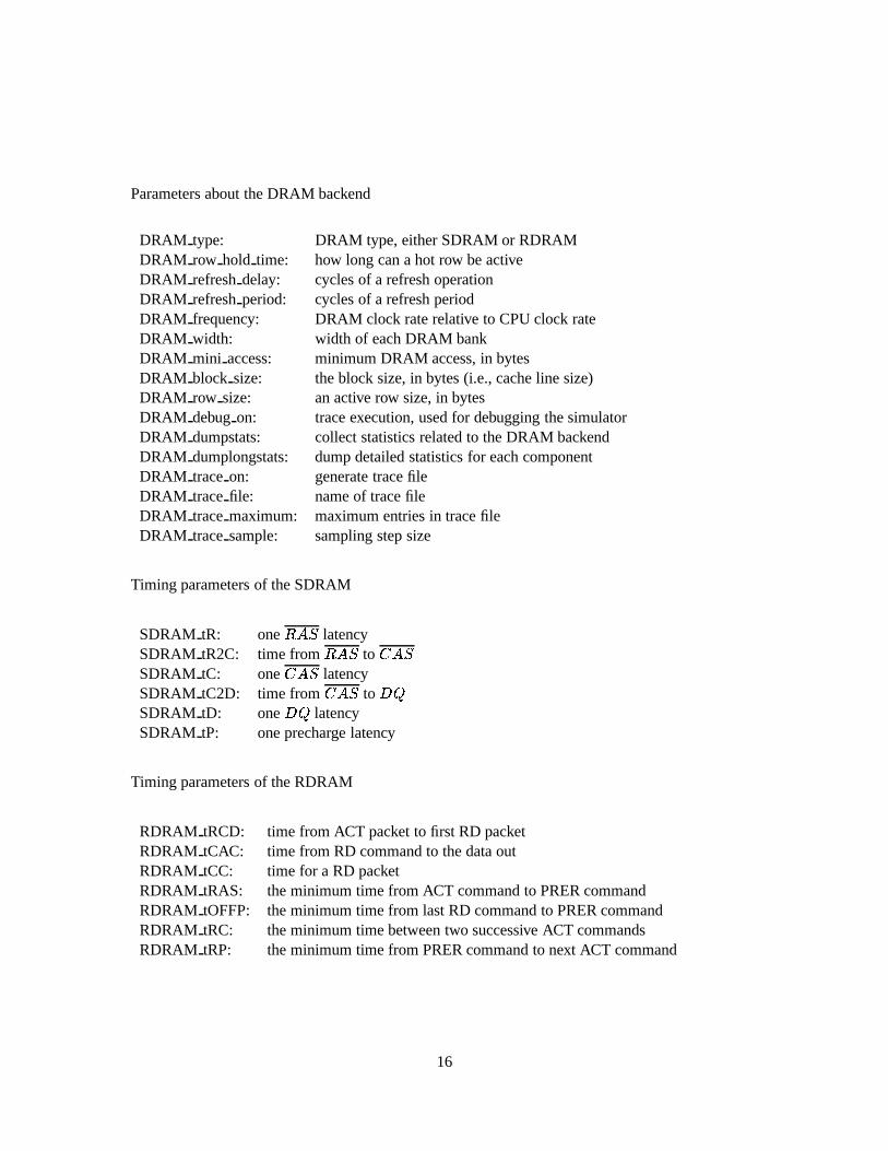
Parameters about the DRAM backend
DRAM type: DRAM type, either SDRAM or RDRAMDRAM row hold time: how long can a hot row be activeDRAM refresh delay: cycles of a refresh operationDRAM refresh period: cycles of a refresh periodDRAM frequency: DRAM clock rate relative to CPU clock rateDRAM width: width of each DRAM bankDRAM mini access: minimum DRAM access, in bytesDRAM block size: the block size, in bytes (i.e., cache line size)DRAM row size: an active row size, in bytesDRAM debug on: trace execution, used for debugging the simulatorDRAM dumpstats: collect statistics related to the DRAM backendDRAM dumplongstats: dump detailed statistics for each componentDRAM trace on: generate trace fileDRAM trace file: name of trace fileDRAM trace maximum: maximum entries in trace fileDRAM trace sample: sampling step size
Timing parameters of the SDRAM
SDRAM tR: one� ���
latencySDRAM tR2C: time from
� ���to� ���
SDRAM tC: one� ���
latencySDRAM tC2D: time from
� ���to� �
SDRAM tD: one� �
latencySDRAM tP: one precharge latency
Timing parameters of the RDRAM
RDRAM tRCD: time from ACT packet to first RD packetRDRAM tCAC: time from RD command to the data outRDRAM tCC: time for a RD packetRDRAM tRAS: the minimum time from ACT command to PRER commandRDRAM tOFFP: the minimum time from last RD command to PRER commandRDRAM tRC: the minimum time between two successive ACT commandsRDRAM tRP: the minimum time from PRER command to next ACT command
16
4 Master Memory Controller
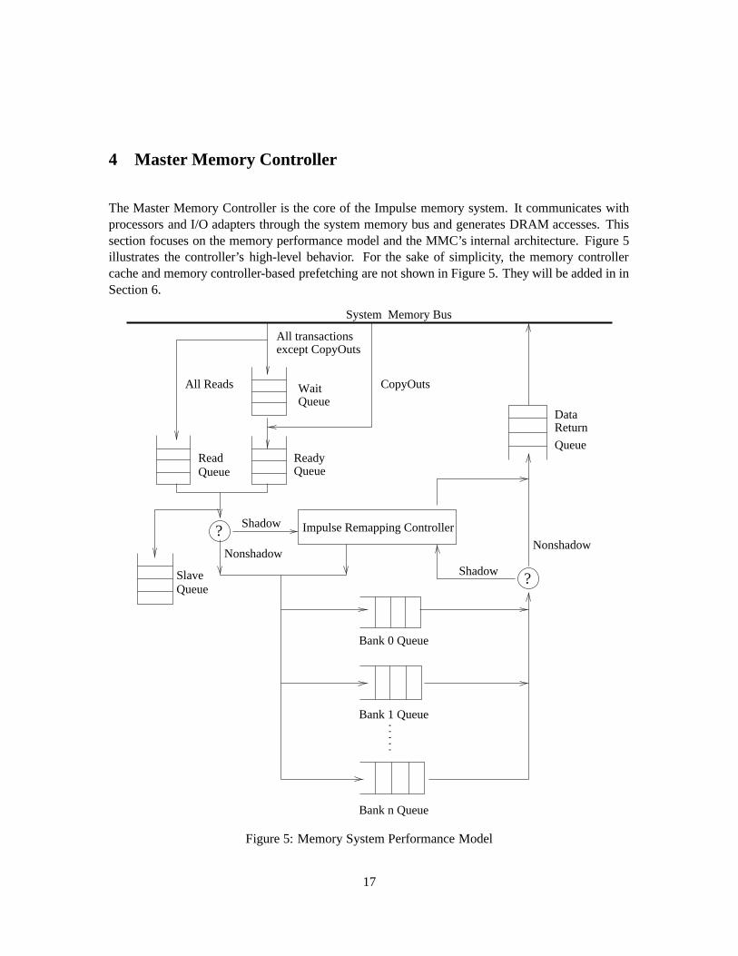
The Master Memory Controller is the core of the Impulse memory system. It communicates withprocessors and I/O adapters through the system memory bus and generates DRAM accesses. Thissection focuses on the memory performance model and the MMC’s internal architecture. Figure 5illustrates the controller’s high-level behavior. For the sake of simplicity, the memory controllercache and memory controller-based prefetching are not shown in Figure 5. They will be added in inSection 6.
Queue
All Reads
Queue
Bank 0 Queue
Bank 1 Queue
Bank n Queue
Data
Nonshadow
?
Shadow
Impulse Remapping ControllerShadow
Nonshadow
All transactionsexcept CopyOuts
Queue
Queue
CopyOuts
?
Wait
Return
Queue
Slave
Read Ready
System Memory Bus
Figure 5: Memory System Performance Model
17

The MMC holds incoming transactions from the system memory bus in several queues and generatesDRAM accesses according to certain rules. Many queues – the wait queue, read queue, ready queue,slave queue, bank queues, and data return queue – are used in the Impulse memory system. Exceptfor the slave queue, all the queues are processed in first-in-first-out order. The bank queues arecontrolled by SMCs; and other queues are controlled by the MMC.
4.1 Wait Queue
All transactions except copyouts are entered in the wait queue. Transactions are processed whenthey reach the head of the wait queue.
When a non-coherent read transaction reaches the head of the wait queue, it is stalled until thecorresponding data is returned from the main memory or the memory controller cache; its addressis then checked against writes in the ready queue. If there are no conflicts (i.e., read and writeaddress does not match), the read data is returned on the system bus; and the read is removed fromthe wait queue. If a conflict is detected, the read transaction will be moved into the ready queue forreissue. Coherent reads are treated identically except that they must wait for their coherency checksto complete. If a coherent read receives a copyout coherency response, its associated read data isdiscarded and the transaction is removed from the wait queue.
When a non-coherent write transaction reaches the head of the wait queue, it is removed from thewait queue and entered in the ready queue. Coherent write transactions are treated identically exceptthat they must wait for their coherency checks to complete.
Copyout transactions are generated when dirty cache data – cache-to-cache copy data, replacedvictim data, or data forced out due to a flush – is being written back to memory. In general, logicallycorrect operation is determined by the order in which transactions are issued to the system bus.Copyout transactions are exceptions since in some instances a transaction that appears on the busbefore a copyout transaction must be treated as if it had occurred after the copyout transaction. Toguarantee transactions in the ready queue are logically correct in order, each client (CPU) mustensure that the copyout is issued to the system bus before sending the Cache Coherency Check(CCC) response for the conflicting transaction. If all transactions in the ready queue are performedin order, the results will be correct. The memory controller can therefore ensure correct behavior byplacing all copyout transactions directly into the ready queue and all other transactions into the waitqueue. Since a transaction does not move from the wait queue to the ready queue until after all CCCresponses have been received for that transaction, any copyouts that should be logically completebefore the transactions will be in the ready queue in front of it.
18

4.2 Read Queue
The read queue is used to reduce the memory latency for read transactions. Read transactions in theread queue are issued to the DRAM backend as quickly as possible; the transactions are not held inthe read queue to wait for the CCC responses. When a read is received by the MMC, it is placedin both the read queue and the wait queue. The read placed in the read queue follows the fast readpath and is called a fast read. The read placed in the wait queue follows a path that is guaranteedto produce correct results and is called a logically ordered read. The fast read is performed withhigher priority and will return incorrect data when conflicts happen. The MMC detects and resolvesthe conflict cases to ensure correct results.
Given that logically ordered reads will always yield the correct results, conflict cases only occurin the window of time between when a fast read is issued and when the corresponding logicallyordered read is issued. Two steps are performed to detect conflicts.
First, at the time that a read exits from the wait queue, the ready queue is checked for any writesto the same address. If no conflicting writes are in the ready queue, the result from the fast readwill be correct. If conflicting writes are found in the ready queue, the results from the fast readmay not be correct and the read will be placed in the ready queue to wait for reissue. In general,the fast read queue has priority over the ready queue, so transactions may stay in the ready queuefor many cycles. When a conflict occurs, the ready queue is temporarily given priority over the fastread queue until the logically ordered read has exited the ready queue and been issued to the DRAMbackend.
Second, whenever a write is issued to the DRAM backend, the wait queue is checked for anyconflicting reads, which may or may not have been issued to the DRAM backend. This check isnecessary because a conflicting write may be issued to the DRAM backend after the fast read isissued to the DRAM backend but before the conflict check is performed. (Note that once a write hasbeen issued to the DRAM backend it is logically complete and is removed from the ready queue.)If such a conflict is found, the MMC will use the results of the logically ordered read instead of thefast read. This may result in false conflict cases, but the returned data is always guaranteed to becorrect.
4.3 Ready Queue
The ready queue holds both copyout transactions taken directly from the system memory bus andtransactions moved from the wait queue. Transactions in the ready queue are ready to be issued tothe DRAM backend. Usually, most transactions in the ready queue are writes. Because the latencyof completing writes is not as critical to system performance as the latency of completing reads, theread queue is given priority over the ready queue in most cases. Figure 6 gives the algorithm usedto issue transactions from the ready queue or the read queue to the DRAM backend.
19

/** Must drain the ready queue until we hit the read when* conflicts have been detected.*/if (drainreadyq) {
next_transaction = FIFO_pop(ready_queue);if (next_transaction is READ)
drainreadyq = 0;}/** Look for possible ready queue overflow*/else if (lengthof(ready_queue) > READYQ_OFLOW ||
empty(read_queue) && notempty(ready_queue)) {next_transaction = FIFO_pop(ready_queue);
}/** Otherwise, issue the head of the read queue.*/else
next_transaction = FIFO_pop(read_queue);
send_to_DRAM_backend(next_transaction);
Figure 6: Code segment to issue transactions to the DRAM backend.
20
4.4 Slave Queue
All transactions that come from the read queue and the ready queue are placed in the slave queue.The primary purpose of the slave queue is to coordinate the use of memory system resources such asthe data busses and memory banks. A transaction in the slave queue is removed when it is removedfrom its bank queue if the transaction is a normal access, or when all of its spawned transactionsare removed from their bank queues if the transaction is a shadow access. Since transactions indifferent bank queues may be processed at different speeds, the slave queue will not be processedin first-in-first-out order.
The slave queue is an obsolete feature from the original system. In the Impulse memory system,the same coordinating functionality has been moved to the DRAM scheduler and SMCs. The onlyuse of the slave queue is to control the total number of outstanding transactions sent to the DRAMbackend, which actually can be accomplished by one single counter-register.
4.5 Bank Queues
Each transaction issued to the DRAM backend affects only one memory bank. Determining whichmemory bank is addressed by a particular transaction is a function of the number and size of memorybanks and the interleaving scheme. A bank queue is placed in a relevant SMC. Currently, we aredesigning an algorithm for reordering the bank queues to reduce the average memory access latency.
4.6 Data Return Queue
The data return queue is used to hold data that has been returned from the DRAM backend, but hasnot yet been sourced to the system bus. Time spent in this queue is added directly to the memorylatency perceived by the processor, so this queue should be empty most of the time. Data returnhas highest priority on the system bus, which means data usually does not need to be placed in thedata return queue. However, there are three circumstances under which data is placed into the datareturn queue. The first case is when a multi-cycle transaction has started on the system bus. Thedata has to wait in the data return queue until the multi-cycle transaction completes. The secondcase is when this transaction’s CCC responses have not been received. The transaction has to stayin the wait queue and the data is placed in the data return queue until its CCC completes. The thirdcase is when the remapping controller and the DRAM backend transmit data on the system bus atthe same time.
21

4.7 Impulse Remapping Controller
Each shadow transaction from the read queue or the ready queue has to be processed by the Impulseremapping controller before accessing the DRAMs. The Impulse remapping controller translateseach shadow address to one or more physical addresses and pushes a transaction into the bankqueue for each generated physical address. When the data associated with the shadow transactionis returned from the DRAM backend, it also has to go back to the remapping controller for furtherprocessing. Details about the Impulse remapping controller are presented in Section 5.
4.8 Flow Control
In a queue-based system, some set of algorithms or protocol rules are required to ensure that noneof the queues overflows. The size of each queue in the Impulse memory system is fixed. So is thenumber of total write data registers in the MMC.
When the MMC runs out of write data registers, it denies all other devices to access the system bus.The ready queue has (1 + the number of write data registers) entries. Since the ready queue can holdat most one read with the rest being writes, it can never overflow. When both the wait queue andthe ready queue are full, the MMC denies all other bus modules to access the system bus. Whenthe wait queue is full but the ready queue is not, the MMC will disallow any transactions exceptcopyouts. The read queue has the same size as the wait queue and every transaction in the readqueue must also have a copy in the wait queue, so the read queue can never overflow. When theslave queue is full, the MMC will stop issuing transactions to it. Flow control for the data returnqueue is accomplished by never issuing a read transaction to the DRAM backend until there is anempty slot in the data return queue.
4.9 Thoughts And Problems
Bank Queue Reordering
No bank queue reordering algorithm has yet been designed. Intuitively, a good reordering algo-rithm should have the following features: giving non-prefetching accesses priority over prefetchingaccesses, determining whether or not to leave a row open after each access, putting accesses to thesame row close to one another, guaranteeing no access will wait in a queue for a very long time, andensuring the logically correct order while performing reordering.
Flow Control of the Bank Queue
22
Flow control on the bank queues is missing in the current design. In the original design, each bankqueue had the same size as the slave queue. The flow control on the slave queue guaranteed nooverflow in any bank queue. However, in Impulse, each transaction placed in the slave queue maysend multiple transactions to the bank queues. The experiments showed that a bank queue with thesame size as the slave queue would easily overflow in Impulse. Possible solutions for this problemare:
� increasing the depth of memory bank, i.e., the size of the bank queue (this is what we areusing now);
� putting the remapping controller before the slave queue, and placing transactions generatedby the remapping controller into the slave queue and stopping the remapping controller whenthe slave queue overflows;
� creating a connection between the remapping controller and the SMCs so that when a shadowdescriptor generates a transaction whose designated bank queue is full, it will be stopped fromgenerating new transactions until there is more room.
Remapping Controller Placement
When to start shadow address translation, i.e., where to put the Impulse remapping controller, mayaffect performance significantly. The remapping controller is placed between the ready queue andthe bank queues in current design. One alternative is to put it in parallel with the wait queue. Sothe address translation can be started when a transaction is placed in the wait queue, i.e., when thetransaction is coming off the system bus. Each design has its advantages and disadvantages.
The Impulse remapping controller could be placed in parallel with the wait queue.
� Pros
– Remapping is started as early as possible, which means remapping overhead is reducedas much as possible.
– Real physical addresses participate in coherency checks. This is critical if data may beaddressed by both shadow address and non-shadow address at the same time and thedata is allowed to be written.
� Cons
– Such a placement may generate huge number of transactions. The sizes of all queueshave to be increased.
– Many more coherency checks are needed.
23
– The address remapping may take many cycles. A transaction whose remapping takesmany cycles will stall transactions behind it in the wait queue.
– The distance between the remapping controller and the DRAM chips is logically long,which means passing data between them is not efficient.
– The performance model has to be modified significantly.
The Impulse remapping controller could be placed after the ready/read queue and before the bankqueues.
� Pros
– This organization is easy to integrate into the original system. Very little change isneeded in the performance model.
– It will not stall other transactions unnecessarily.
– Communication between the remapping controller and memory banks is efficient.
� Cons
– Shadow physical addresses, not real physical addresses, participate in coherency check.
– The address remapping is started relatively late.
4.10 Source Codes And Configurable Parameters
Source codes
mmc/mmc aux.c: some auxiliary functionsmmc/mmc init.c: initialization of memory controllermmc/mmc debug.c: debugging supportmmc/mmc main.c: performance modelmmc/mmc stat.c: statistics collectionmmc/mmc global.h: definition of global variablesmmc/mmc param.h: definition of parametersmmc/mmc.h: definition of major data structuresmmc/mmc func.h: definition of functionsmmc/mmc gen def.h: some useful macrosmmc/mmc stat.h: data structures to record statistics
Almost all parameters related to the performance model are hardcoded in current implementation.Parameters about the remapping controller can be found in section 5.
24

5 Impulse Remapping Controller
To data return queue
1
2
3
4
5
6
From read or ready queue
Control Registers
Control Logic
ALUs
Impulse Remapping Controller
DRAM Scheduler
MTLB
Descriptor 0
SRAM buffer
Figure 7: Impulse Remapping Controller Block Diagram
Figure 7 shows the internal structure of the Impulse remapping controller. The Impulse remappingcontroller contains several shadow descriptors (seven in current design) and a memory controllerTLB. Each shadow descriptor includes some control registers, a small SRAM cache, a simple ALUunit, and the assembly logic. The control registers store remapping information such as remap-ping type and shadow address space region. The small cache holds remapped data prefetched fromDRAM. The simple ALU unit translates shadow addresses to pseudo-virtual addresses, which aretranslated into real physical addresses by the MTLB. The assembly logic gathers sparse data re-trieved from DRAM into dense cache lines. The functionality of shadow descriptors ALUs has yet
25

to be completely specified. For now, we assume only integer operations, all of which complete in asingle memory cycle.
The control registers are memory-mapped and have to be set with appropriate values before beingused to perform remapping. Only the operating system is allowed to configure the remapping con-troller. All the shadow descriptors use the same memory addresses for their control registers. Whenthe operating system tries to configure a shadow descriptor, it will first send the index number of theselected descriptor to the remapping controller, and then write information to the control registersin that shadow descriptor.
Only one read or write transaction is allowed to access a shadow descriptor at one time. The remap-ping controller has a queue for each shadow descriptor to hold the waiting transactions in first-in-first-out order. The size of each queue equals the size of the slave queue.
Currently, the Impulse remapping controller supports the following remapping algorithms: stridedscatter/gather; scatter/gather through an indirection vector; no-copy page coloring; and no-copysuperpage formation. Each different remapping algorithm uses different information and procedureto remap data. The following subsections describe these remapping algorithms in detail.
5.1 Strided Scatter/Gather
Non-unit stride accesses are common in real applications. Examples include accessing matrices incolumn-major order when the matrices are stored in row-major order, accessing the same field ofevery record in a database, and accessing tiles of a dense matrix. Applications with non-unit strideaccesses may load cache lines in which most of the data goes unused by the CPU. This causesproblems like cache pollution, low bus utilization, and low cache hit ratios. Impulse can createcache-friendly aliased data structures in shadow memory such that these dense structures containonly the strided data accessed by the CPU. The following example illustrates creating and usingsuch an alias vector for a program that calculates the sum of all employees’ salaries.
struct record {...float salary;...
} all_employees[TOTAL_EMPLOYEES];
foo() {float sum = 0;float *salaries = Impulse_remap(sizeof(struct record),
sizeof(float),OFFSET(struct record, salary),TOTAL_EMPLOYEES, ...);
for (int i = 0; i < TOTAL_EMPLOYEES; i++)
26

sum += salaries[i];}
Impulse remap() is a system call to set up the remapping controller. It first chooses a shadowdescriptor and then writes necessary information into it. In our example, the information that theremapping controller needs includes:
saddr start: starting shadow address – the physical address of salaries[0];stride size: stride size – sizeof(struct record);object size: object size – sizeof(float);object count: number of objects – TOTAL EMPLOYEES;object offset: offset of required object in the stride –
(&(all employees-�
salary) � all employees);ptable ptr: a dense, flat page table to map the original data structure all employees
from virtual pages to physical pages.
When the remapping controller receives a shadow access saddr, it performs as follows.
0. Calculate the number of DRAM accesses needed to gather a cache line:
if object size � cache line size, count = cache line size / object size;
if object size � cache line size, count = 1.
This step is actually done when the mapping is initialized. Once the mapping is set, it willnot change until reset.
1. Calculate the offset in the shadow address space:
soffset = saddr � saddr start.
2. Calculate the index of the stride that contains the requested object:
index = soffset / object size.
If object size � cache line size, calculate the offset of the requested cache line in the object:
coffset = soffset % object size.
3. Calculate the offset in the pseudo-virtual address space:
voffset = index � stride size + object offset (+ coffset, if object size � cache line size);
4. Look up the physical address paddr in the MTLB. If the lookup misses in the MTLB, theMTLB will access physical memory for the relevant page table entry.
5. Access physical memory at physical address paddr forobject size bytes, if object size � cache line size;cache line size bytes, if object size � cache line size.
27

6. if ( - -count� 0), calculate the next item’s offset in pseudo-virtual address space:
voffset += stride size;goto step 4;
Steps 4-6 are fully pipelined, so a new physical address can be generated each cycle. This pipelineis stalled only when an MTLB miss occurs in step 4. After all the memory accesses complete, therelevant shadow descriptor will create a dense cache line and send it back to the requester throughthe system bus.
5.2 Scatter/Gather Through An Indirection Vector
This type of remapping is used by applications that access their major data structures through indi-rection vectors. The following is a simple example of using this remapping.
foo() {int iv_array[IVSIZE];double major_data[SIZE];
#ifndef Use_Impulse_Optimization/* Non-impulse version */for (i = 0; i < IVSIZE; i++)
... = ... major_data[iv_array[i]] ... ;#else
/* Impulse version */double * alias_array = Impulse_remap (...);for (i = 0; i < IVSIZE; i++)
... = ... alias_array[i] ...;#endif}
The following information is needed for performing a scatter/gather mapping through an indirectionvector.
saddr start: starting shadow addressstride size: stride sizeobject size: object sizeobject count: number of objectsobject offset: offset of required object in the strideiv elem size: element size of the indirection vectoriv paddr start: starting physical address of the indirection vectorptable ptr: dense, flat page table mapping original data structureiv buffer: a cache line to store elements of the indirection vector
28

The shadow descriptor takes the following actions to gather a cache line of data addressed by theshadow address saddr.
0. Calculate how many DRAM accesses are needed to gather a cache line:
if object size � cache line size, count = cache line size / object size;
if object size � cache line size, count = 1.
This step is actually done when the mapping is initialized. Once the mapping is set, it willnot change until explicitly reset.
1. Calculate the offset in the shadow address space:
soffset = saddr � saddr start.
2. Calculate the index of the requested object:
index = soffset / object size.
If object size � cache line size, calculate the offset of the requested cache line in the object
coffset = soffset % object size.
3. Calculate the physical address for the associated element of the indirection vector:
iv paddr = iv paddr start + index � iv elem size;
4. If iv paddr is not in the IV buffer, the shadow descriptor fetches a whole cache line containingthe required indirection vector element from physical memory into the IV buffer. The shadowdescriptor then interprets the element to get its value rindex, which is the index into theoriginal array.
5. Calculate the offset in pseudo-virtual address space:
rindex � stride size + object offset (+ coffset, if object size � cache line size).
6. Look up the physical address paddr in the MTLB. If the lookup misses in MTLB, the MTLBwill access physical memory for the relevant page table entry.
7. Access physical memory at physical address paddr forobject size bytes, if object size � cache line size;cache line size bytes, if object size � cache line size.
8. if ( - -count � 0), calculate the physical address of the next indirection vector element:iv paddr += iv elem size;goto step 4;
When an application sets up scatter/gather remapping through an indirection vector via the operatingsystem, the operating system moves the indirection vector into a contiguous physical space, so thephysical addresses of indirection vector elements can be used directly by the remapping controller.
29

As with the strided remapping, steps 4 to 6 are pipelined to generate one physical address eachcycle. MTLB misses stall the pipeline.
5.3 No-copy Page Coloring
No-copy page coloring is designed to optimize data layout in physically indexed caches. The ex-ample in Figure 8 explains how no-copy page coloring works. This example maps data structureA to the third quadrant of a physically indexed L2 cache. The operating system first allocates ashadow address space four times of the size of L2 cache and then creates a page table in the CPUto map each quarter of A to an appropriate region in the allocated shadow address space, as shownin Figure 8. Assuming the allocated shadow address space is L2-cache-size-aligned, all the greyboxes in the shadow address space are mapped into the same portion of the L2 cache. Note that thewhite spaces in shadow address space are wasted in this design. Since shadow address space is notdirectly backed up by real physical memory, wasting shadow address space will not waste any realphysical memory.
L2 Cache:
Shadow
Space
color offset
Logical Layout of A:
Cache way size
color
size
Physical
Figure 8: Map A into the third quadrant of L2 cache
The following information is needed to perform the no-copy page-coloring remapping.
30
saddr start: starting shadow addresscache size: effective cache way size (size / associativity)color size: size of the region to which shadow data is mappedcolor offset: offset in the region to which shadow data is mappedptable ptr: a page table mapping original data structure
When a shadow descriptor receives a shadow access saddr, it takes the following actions.
1. Calculate the offset in the shadow address space:
soffset = saddr - saddr start.
2. Calculate the index of the color where the requested object lies:
index = soffset / cache size;
and the offset of the requested data in this color:
coffset = soffset % cache size - color offset.
3. Calculate the offset in pseudo-virtual space:
voffset = index � color size + coffset.
4. Look up the physical address paddr in the MTLB. If the lookup misses in MTLB, the MTLBwill access physical memory for the relevant page table entry.
5. Access physical memory at physical address paddr forcache line size bytes.
5.4 No-copy Superpage Formation
This type of remapping creates superpages from disjoint physical pages without copying[1]. It canbe used by applications which suffer from poor TLB performance. This remapping needs only thestarting shadow address and the page table. Since the offset in shadow memory is the same as theoffset in pseudo-virtual memory, the physical address generation is simply two steps: calculate theoffset in the shadow address space and perform the MTLB lookup.
5.5 Thoughts And Problems
ALU
There are many divisions and multiplications in the remapping algorithms described above. If adivision is really needed, the latency of a division operation surely will not be the assumed one
31

cycle. If the object size (for scatter/gather) or cache line size (for page coloring) is a power oftwo, a division can be replaced by a logic right shift operation. Likewise, if the stride size (forscatter/gather) or the color size is a power of two, a multiplication can be replaced by a logic leftshift operation. In real applications, the object size is usually a power of two but the stride size isoften not. We will have to determine whether or not Impulse should support division. If no divisionunit is used, the compiler must find a way to pad each stride or each object to be a power of two.If both the stride size and object size are powers of two, all the arithmetic operations are additions,or subtractions, or logic operations. Figure 9 shows how easily the remapping can be done for themost complicated remapping — scatter/gather through an indirection vector — when the size ofeach data item is a power of two.
Step 7: To DRAM
Physical address: physical page number page offset
Access DRAM
objsizeindex
iv_elem_sizeindex
iv_paddr_start
saddr_start
Step 1: no calculation
Step 3: one addition
Step 4: one memory access
Step 2: no calculation
0 0.....
Access memory for "rindex"
0 ..... 0 rindex stride offset
saddr:
page offset
Step 6: MTLB lookup MTLB
pvirtual page number Step 5: no calculationAssemble pseudo-virtual address:
soffset
Figure 9: Address manipulations in scatter/gather through an indirection vector, assumingstride size, object size, and iv elem size all are powers of two.
Security/Boundary Checks
32

Security/boundary checks are missing. When and how to perform boundary checks is still unde-cided. The simplest way is to use a page table. If the page table shows that a pseudo-virtual addressis out of bounds, the transaction will be aborted. But this strategy may raise problems when a cacheline is gathered across page boundaries. For example, if the first half of a cache line should be gath-ered from page A, which is valid, and the second half should be gathered from page B, which notvalid, this cache line cannot be correctly gathered because there is no way to fetch its second half.A simple solution is to put restrictions on remapping — never allowing scatter/gather to cross pageboundaries. Another solution is to check every pseudo-virtual address. For scatter/gather throughan indirection vector, we also have to check every access to the indirection vector. If the boundarycheck should be applied, we must decide whether to handle it in parallel with other operations or tomake it an independent stage in the simulation model.
Page Faults
The current simulator does not have a mechanism to handle page faults generated by the MTLB.There are two obvious solutions: first, abort this transaction and let CPU load the page into mainmemory, then reissue this transaction; second, add an extra communication mechanism between theCPU and the MMC so that the MMC can instruct the CPU to load a required page, and the CPU canthen inform the MMC when the required page has been loaded.
Number of Control Registers
Not all the remapping algorithms use the same number of control registers. If all shadow descrip-tors are given the same number of control registers, some control registers will not be used by someremapping algorithms. If control registers are expensive, we have to find a way to conserve controlregisters. One possible solution is to give each shadow descriptor different number of control reg-isters and let it handle only one or several specified remappings, depending on how many controlregisters it has. Another solution is to convert “unused” control registers into data buffers.
Waiting Queue Control
The current design uses a big waiting queue for each shadow descriptor, which seems unreasonable.One alternative is to use a global queue for all shadow descriptors. If the global queue is notlarger than the slave queue, no extra flow control is required. If the global queue is smaller thanthe slave queue, the MMC has to be stopped when the global queue is full. A global queue willnot maintain first-in-first-out ordering, however. Transactions in the global queue will be started assoon as the corresponding shadow descriptor becomes available, which will happen in a dynamicallydetermined order.
33

5.6 Source Codes And Configurable Parameters
Source codes
mmc/mapcontroller.c: simulator of the Impulse remapping controllermmc/mapcontroller.h: header file
Parameters for the Impulse remapping controller
Shadow Region Mask: the shadow address spaceNum descriptors: number of shadow descriptorsDescriptor start cycles: overhead to start a new mappingDescriptor add cycles: cycles of an addition/subtraction operationDescriptor div cycles: cycles of a division operationDescriptor mul cycles: cycles of a multiple operationDesQueue num: how many queues in the remapping controllerDesQueue len: size of each queue
34

6 MC-based Prefetching and MCache
Read
Queue
Slave
Queue
Data
Return
Queue
Impulse Remapping ControllerNonshadow
Shadow
Memory Controller Cache
Shadow
System Memory Bus
?
Wait
Queue
Queue
Ready
CopyOuts
Nonshadow
Bank Queues
All transactionsexcept CopyOuts
All Reads
Figure 10: The memory performance model with the MCache
The second important feature of Impulse is its support for prefetching at the memory controller– MC-based prefetching. MC-based prefetching uses a small SRAM cache – MCache – in thememory controller to reduce the effective memory latency perceived by the processor. Specifically,the Impulse memory controller can speculatively load data from DRAM into the MCache. If amemory request hits in the MCache, the MMC can quickly provide the requested data without goingthrough a full DRAM access. Figure 10 shows the MCache’s position in the memory performancemodel. The MCache introduces one more cycle into the critical timing path of a memory access.Since the MMC is fully pipelined, it adds only one cycle into a sequence of continuous accesses.Compared to 50-plus-cycle memory latency, one extra cycle is insignificant. MC-based prefetchingis more important for shadow accesses than for non-shadow accesses. Each shadow access mustgo through the remapping controller, which may take up to hundreds of cycles. It is crucial for theMMC to start loading shadow data as early as possible to hide the cost of remapping.
35

6.1 MC-based Prefetching
We face several challenges during the design of MC-based prefetching. The first challenge is to de-termine what kind of algorithm MC-based prefetching should use and how aggressive it should be?At the point that this document is being written, we use a simple algorithm: sequential prefetchingfor non-shadow data, and configurable-stride prefetching for shadow data.
The second challenge is to decide when to generate a prefetch address and when to issue a prefetch.A prefetch address may be used immediately, or be saved and then used later. A prefetch does notneed to perform coherency check regardless of whether the transaction spawning the prefetch iscoherent or not because the coherency check will be performed when the CPU issues a memoryrequest for the prefetched data.
The possible times in the performance model to generate prefetch addresses are:
1. when transactions are placed in the wait queue;
2. when transactions come off the wait queue;
3. when transactions return from the DRAM backend.
Which one is better depends on applications’ access patterns. For example, for applications thatgenerate bursts of memory transactions, it may be the best to generate prefetch addresses whentransactions return from the DRAM backend. For applications that generate sequential memorytransactions, generating prefetch addresses when transactions are placed in the wait queue may bethe best choice.
The possible times to issue prefetches are:
1. when a prefetch address is generated;
2. when both the read queue and the ready queue are empty;
3. when no outstanding transactions exist in the MMC.
If one of the last two options is selected, a prefetch will not be issued at the time when the addressis generated, and the MMC will have to save the prefetch address somewhere. To issue a prefetchwhen its address is being generated seems like a good choice because the MMC is lightly loaded inthe current uniprocessor system. When the memory system is heavily loaded, generating a prefetchaddress for every read transaction will make the MMC and DRAM backend too busy to completenormal transactions within reasonable time. On the another hand, issuing prefetches when both the
36
read queue and the ready queue are empty or when the MMC is free will cause every few prefetches.These facts must be considered in the design of MC-based prefetching.
Not all the combinations of the options mentioned above are valid. For example, combining case2 of generating prefetch addresses with case 2 of issuing prefetches does not make sense; andcombining case 1 of generating prefetch addresses with case 1 of issuing prefetches allows a prefetchto go ahead of the transaction that triggered the prefetch.
Since address remapping may take many cycles, a prefetch transaction may occupy a shadow de-scriptor for a long time. If a non-prefetch transaction needs a shadow descriptor being used byan ongoing prefetch, it has to wait until the prefetch transaction completes its address translation.Because the cycles waiting for a shadow descriptor are directly added to the memory latency, theprefetch transaction should be either suspended or aborted. The current simulator does neither sus-pension nor abortion. The prefetch strategies used in the current design have worked well for theapplications that we have tested. Other applications may benefit from a more sophisticated algo-rithm.
6.2 MCache Organization
The MCache includes a modest-size buffer to store prefetched, non-shadow data and a small buffer(two to four cache lines) for each shadow descriptor to store prefetched, shadow data. The smallbuffer for each shadow descriptor is fully-associative, and its design is trivial. Except where statedotherwise, the following discussion uses the MCache to represent the buffer for non-shadow data.
The MCache uses a FIFO replacement policy. The behavior of the MCache is quite different fromthe behavior of CPU caches. Since the most frequently used data should reside in the CPU caches,the MCache data will probably not be used frequently. Replacement policies such as LRU and NRUsimply do not work well with the MCache. Our experiments show that FIFO outperforms LRU inall cases tested.
The MCache is four-way associative, physically indexed, and physically tagged. Its normal size is4kilobytes. Its line size equals the size of an L2 cache line. The MCache uses a write-invalidateprotocol, i.e., any write memory transaction invalidates matched data in the MCache. As a result,data in the MCache can never be dirty, which means that victim data can simply be discarded whena conflict occurs. Each MCache line has the following format:
used (1bit) state (1bit) physical tag (22bits) data (32-128bytes)
The used bit indicates whether or not this line is in use. The state bit indicates the state of this line —either Prefetching or Valid. The tag is the most significant 22 bits of a physical address. Prefetching
37

means that the data is being prefetched right now but have not returned from physical memory. Afterthe prefetched data have returned, the state bit will be changed to Valid. In order to avoid generatingduplicate DRAM accesses when a cache line being prefetched is also requested by a processor, anMCache line is reserved when a prefetch transaction is issued. If an access needs the same data thatan ongoing prefetching transaction is fetching, it will hit in the MCache and wait for the return ofthe desired data. A line reserved for an ongoing prefetch transaction will not be victimized beforethe prefetched data return. In the case that all of four lines that a prefetch transaction can use areoccupied by other ongoing prefetch transactions, the new prefetch transaction is simply discarded.
6.3 Thoughts And Problems
About MCache
Currently, non-shadow data and shadow data have independent buffers. Would it be beneficial toput buffers in all shadow descriptors together, or to coalesce all buffers in the MMC? The FIFOreplacement policy outperforms both LRU and NRU in our experiments. It will be very interestingto test more policies. For example, what kind of performance would “Most Recently Used” yield?
About MC-based Prefetching
The following questions need to be answered. When should the MMC generate prefetch addresses?When should it issue prefetches? Should it, under what circumstances, abort ongoing prefetch trans-actions? What kind of algorithm should MC-based prefetching eventually use, and how aggressiveshould it be? Should the MMC generate a prefetch address for each load transaction, for only asubset of load transactions, or for more types of transactions other than just load.
6.4 Source Codes And Configurable Parameters
Source codes
mmc/mmc cache.c: memory controller cachemmc/mmc prefetch.c: MC-based prefetchingmmc/mmc.h: data structures used by MCache module
Parameters about MC-based prefetching and the MCache
38
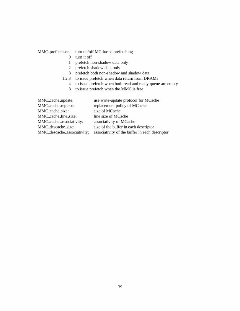
MMC prefetch on: turn on/off MC-based prefetching0 turn it off1 prefetch non-shadow data only2 prefetch shadow data only3 prefetch both non-shadow and shadow data
1,2,3 to issue prefetch when data return from DRAMs4 to issue prefetch when both read and ready queue are empty8 to issue prefetch when the MMC is free
MMC cache update: use write-update protocol for MCacheMMC cache replace: replacement policy of MCacheMMC cache size: size of MCacheMMC cache line size: line size of MCacheMMC cache associativity: associativity of MCacheMMC descache size: size of the buffer in each descriptorMMC descache associativity: associativity of the buffer in each descriptor
39

7 Memory Controller TLB
The MMC first translates shadow addresses to pseudo-virtual addresses, and then to physical ad-dresses. The mapping from pseudo-virtual to physical addresses is like the one from virtual to phys-ical addresses in the CPU/MMU. Just as the CPU uses the TLB (Translation Lookaside Buffer), theMMC uses a memory controller TLB (MTLB) to accelerate the pseudo-virtual to physical transla-tions.
7.1 Hardware Design
When an application issues a system call to set up a remapping, the operating system creates adense, flat page table to store the pseudo-virtual-to-physical translations of the data structure beingremapped. We refer to this page table as the memory controller page table. Since the memorycontroller page table is dense and flat, it can be indexed by the virtual offset of the original datastructure. Each 4-byte entry of the memory controller page table has the following format:
valid (1) ref (1) modify(1) fault(1) frame(20) unused (8)
The valid bit indicates whether this mapping is valid. The reference bit indicates whether a pagehas been referenced. This bit is set on the first MTLB miss for the page. The modify bit indicateswhether a page has been written. This bit is set on the first write reference for the page. The fault bitindicates whether the page is in the main memory. The frame is the physical page number. Becausewe assume 32-bit physical address and four-kilobytes page size, the frame has 20 bits. The eightunused bits are reserved for future expansion.
In the simulator, the MTLB has configurable size and associativity, uses a Not Recently Used (NRU)replacement policy, and has a one-cycle access latency. Each entry of the MTLB has the followingformat:
valid (1bit) locked (1bit) tag (20bits) refcount (16bits) PTE (4 bytes)
The valid bit indicates whether or not this mapping is valid. The locked bit indicates whether ornot this entry is reserved for an ongoing MTLB-fill transaction. A tag is formed by a pseudo-virtual page offset and the index number of the shadow descriptor that generated this pseudo-virtualaddress. The refcount bit records the total number of references to the page. It is used to implementthe NRU replacement policy. To avoid overflow in refcount, refcount is reset after a certain numberof translations have accessed the MTLB.
40

A small buffer inside the MTLB is used to cache the page table entries loaded from physical mem-ory. Each MTLB miss checks the buffer first before sending a fill request to DRAM. If an MTLBmiss hits in the buffer, it only takes one extra cycle to load the translation into the MTLB. If it missesin the buffer, the MTLB will generate a fill request to load a cache line containing 32 translationsfrom physical memory. The following pseudo-code describes the behavior of the MTLB when itreceives a lookup request.
If (lookup hits in the MTLB) {if (the entry’s valid bit is set)
goto hit_MTLB;else /* the entry’s valid bit is not set */
issue an exception;return;
}else { /* the lookup failed in the MTLB */
check for a match in the buffer;if (hit in buffer) {
take one cycle to load the translation into the MTLB;goto hit_MTLB;
}else { /* missed in buffer */
launch a read transaction to load translation from memory;wait until read return fills the buffer;allocate an entry in the MTLB, and load translation into the MTLB;goto hit_MTLB;
}}
hit_MTLB:/** form physical address*/merge physical page frame number from the MTLB entrywith page offset portion of the pseudo-virtual address;
/** Set reference/modified bits appropriately.* Write it back to main memory if the translation is changed.*/if (this is the first reference/write on the given page) {
set reference/modified bit;write the translation back to main memory;
}
41

The translations in the MTLB must be kept consistent with the ones in main memory. If the MTLBdid not write the modified translations back to main memory immediately, fatal errors would occur.For example, if a given page translated by the MTLB is written and the MTLB does not writethe translation back to physical memory before the page is evicted out of physical memory, theoperating system will not know that the modified bit was set and will not write the page back todisk. Consequently the writes at the page will be lost.
In the simulator, the MTLB fill or write-back requests are non-coherent memory transactions and areput in an independent queue which has higher priority than both the read queue and the ready queue.Any MTLB access should be completed as soon as possible so that it can release the dependenttransactions as early as possible, so we MTLB-initiated transactions the highest priority.
7.2 Source Codes And Configurable Parameters
Source codes
mmc/mmc tlb.c: MTLB simulatormmc/mapcontroller.h: data structures related MTLB
Parameters related to MTLB
MMCTLB usetlb: whether or not to use MTLBMMCTLB dumpstats: turn on/off statistics collectionMMCTLB debug: turn on/off debugging printingMMCTLB numentries: number of entries in MTLBMMCTLB associativity: associativity of MTLBMMCTLB buffersize: size of the buffer in MTLBMMCTLB resetcount: the number of transactions needed to reset “refcount”MMCTLB tagcheck cycles: cycles of MTLB tag check
42

References
[1] M. Swanson, L. Stoller, J. Carter. Increasing TLB Reach Using Superpages Backed by ShadowMemory. In 25th Annual International Symposium on Computer Architecture, July 1998.
[2] L. Stoller, M. Swanson, R. Kuramkot. Paint: PA Instruction Set Interpreter. Technical ReportsUUCS-96-009, University of Utah, July 1997
[3] J. Veenstra, R. Folwer. MINT Tutorial and User Manual. Technical Reports 452, University ofRochester, Aug. 1994.
[4] T. Hotchkiss, N. Marschke, R. McClosky. A New Memory System Design for Commercialand Technical Computing Products In HP Journal, Vol.47 No.1, pages 44-51, Feb. 1996.
[5] W. Bryg, K. Chan, N. Fiduccia. A High-Performance, Low-Cost Multiprocessor Bus for Work-stations and Midrange Servers. In HP Journal, Vol.47 No.1, pages 18-23, Feb. 1996.
[6] IBM Advance, 256Mb Synchronous DRAM – Die Revision A. Aug. 1998.
[7] IBM Advance, 64Mb Direct Rambus DRAM. Nov. 1997.
[8] L. Schaelicke. DRAM Backend for Impulse Memory Controller. Unpublished report, April1998.
[9] Kitty Hawk Memory System, External Reference Specification, Revision B. May 1995
[10] R. Schumann. Design of the 21174 Memory Controller for DIGITAL Personal Workstations.Digital Technical Journal, Vol.9 No.2, Nov. 1997
43