IS61WV25616EDBLL IS64WV25616EDBLL - … · 2 Integrated Silicon Solution, Inc. — Rev. A1...
14
Integrated Silicon Solution, Inc. — www.issi.com 1 Rev. A1 02/10/2017 Copyright © 2017 Integrated Silicon Solution, Inc. All rights reserved. ISSI reserves the right to make changes to this specification and its products at any time without notice. ISSI assumes no liability arising out of the application or use of any information, products or services described herein. Customers are advised to obtain the lat- est version of this device specification before relying on any published information and before placing orders for products. Integrated Silicon Solution, Inc. does not recommend the use of any of its products in life support applications where the failure or malfunction of the product can reason- ably be expected to cause failure of the life support system or to significantly affect its safety or effectiveness. Products are not authorized for use in such applications unless Integrated Silicon Solution, Inc. receives written assurance to its satisfaction, that: a.) the risk of injury or damage has been minimized; b.) the user assume all such risks; and c.) potential liability of Integrated Silicon Solution, Inc is adequately protected under the circumstances IS61WV25616EDBLL IS64WV25616EDBLL FEATURES • High-speed access time: 8, 10 ns • Low Active Power: 85 mW (typical) • Low Standby Power: 7 mW (typical) CMOS standby • Single power supply — VDD 2.4V to 3.6V (10 ns) — VDD 3.3V ± 10% (8 ns) • Fully static operation: no clock or refresh required • Three state outputs • Data control for upper and lower bytes • Industrial and Automotive temperature support • Lead-free available • Error Detection and Error Correction 256K x 16 HIGH SPEED ASYNCHRONOUS CMOS STATIC RAM WITH ECC DESCRIPTION The ISSI IS61/64WV25616EDBLL is a high-speed, 4,194,304-bit static RAMs organized as 262,144 words by 16 bits. It is fabricated using ISSI's high-performance CMOS technology. This highly reliable process coupled with innovative circuit design techniques, yields high- performance and low power consumption devices. When CE is HIGH (deselected), the device assumes a standby mode at which the power dissipation can be re- duced down with CMOS input levels. Easy memory expansion is provided by using Chip Enable and Output Enable inputs, CE and OE. The active LOW Write Enable (WE) controls both writing and reading of the memory. A data byte allows Upper Byte (UB) and Lower Byte (LB) access. The IS61/64WV25616EDBLL is packaged in the JEDEC standard 44-pin TSOP-II and 48-pin Mini BGA (6mm x 8mm). FUNCTIONAL BLOCK DIAGRAM FEBRUARY 2017 Memory Lower IO Array- 256Kx8 ECC Array- 256K x4 Decoder I/O Data Circuit ECC Column I/O IO0-7 Control Circuit A0-A17 IO8-15 8 ECC 8 8 8 12 12 Memory Upper IO Array- 256Kx8 ECC Array- 256K x4 8 4 4 8 /CE /OE /WE /UB /LB
Transcript of IS61WV25616EDBLL IS64WV25616EDBLL - … · 2 Integrated Silicon Solution, Inc. — Rev. A1...

Integrated Silicon Solution, Inc. — www.issi.com 1Rev. A102/10/2017
Copyright © 2017 Integrated Silicon Solution, Inc. All rights reserved. ISSI reserves the right to make changes to this specification and its products at any time without notice. ISSI assumes no liability arising out of the application or use of any information, products or services described herein. Customers are advised to obtain the lat-est version of this device specification before relying on any published information and before placing orders for products.
Integrated Silicon Solution, Inc. does not recommend the use of any of its products in life support applications where the failure or malfunction of the product can reason-ably be expected to cause failure of the life support system or to significantly affect its safety or effectiveness. Products are not authorized for use in such applications unless Integrated Silicon Solution, Inc. receives written assurance to its satisfaction, that:a.) the risk of injury or damage has been minimized;b.) the user assume all such risks; andc.) potential liability of Integrated Silicon Solution, Inc is adequately protected under the circumstances
IS61WV25616EDBLLIS64WV25616EDBLL
FEATURES• High-speedaccesstime:8,10ns
• LowActivePower:85mW(typical)
• LowStandbyPower:7mW(typical) CMOS standby
• Singlepowersupply
— Vdd2.4Vto3.6V(10ns) — Vdd 3.3V±10%(8ns)
• Fullystaticoperation:noclockorrefresh required
• Threestateoutputs
• Datacontrolforupperandlowerbytes
• IndustrialandAutomotivetemperaturesupport
• Lead-freeavailable
• ErrorDetectionandErrorCorrection
256K x 16 HIGH SPEED ASYNCHRONOUS CMOS STATIC RAM WITH ECC
DESCRIPTIONThe ISSI IS61/64WV25616EDBLL is a high-speed,4,194,304-bit static RAMs organized as 262,144 words by 16 bits. It is fabricated using ISSI's high-performance CMOS technology.Thishighly reliableprocesscoupledwith innovative circuit design techniques, yields high-performance and low power consumption devices.
WhenCE isHIGH (deselected), thedeviceassumesastandby mode at which the power dissipation can be re-duced down with CMOS input levels.
EasymemoryexpansionisprovidedbyusingChipEnableandOutputEnableinputs,CE and OE.TheactiveLOWWriteEnable(WE) controls both writing and reading of the memory.AdatabyteallowsUpperByte(UB)andLowerByte(LB) access.
TheIS61/64WV25616EDBLLispackagedintheJEDECstandard44-pinTSOP-II and48-pinMiniBGA(6mmx8mm).
FUNCTIONAL BLOCK DIAGRAM
FEBRUARY 2017
Memory Lower IO
Array-256Kx8
ECC Array-256K
x4
Decoder
I/O Data Circuit
ECCColumn I/O
IO0-7
Control Circuit
A0-A17
IO8-15
8
ECC8
8
8
12
12
Memory Upper IOArray-
256Kx8
ECC Array-256K
x4
8 4 48
/CE/OE/WE/UB/LB

2 Integrated Silicon Solution, Inc. — www.issi.comRev. A1
02/10/2017
IS61/64WV25616EDBLL
TRUTH TABLE I/O PIN
Mode WE CE OE LB UB I/O0-I/O7 I/O8-I/O15 VDD Current
NotSelected X H X X X High-Z High-Z Isb1, Isb2
OutputDisabled H L H X X High-Z High-Z Icc X L X H H High-Z High-Z
Read H L L L H dout High-Z Icc H L L H L High-Z dout H L L L L dout dout
Write L L X L H dIn High-Z Icc L L X H L High-Z dIn L L X L L dIn dIn
PIN DESCRIPTIONSA0-A17 Address Inputs
I/O0-I/O15 DataInputs/Outputs
CE ChipEnableInput
OE OutputEnableInput
WE WriteEnableInput
LB Lower-byteControl(I/O0-I/O7)
UB Upper-byteControl(I/O8-I/O15)
NC No Connection
Vdd Power
GND Ground
12345678910111213141516171819202122
44434241403938373635343332313029282726252423
A0A1A2A3A4CE
I/O0I/O1I/O2I/O3VDDGNDI/O4I/O5I/O6I/O7WEA5A6A7A8A9
A17A16A15OEUBLBI/O15I/O14I/O13I/O12GNDVDDI/O11I/O10I/O9I/O8NCA14A13A12A11A10
PIN CONFIGURATIONS
44-Pin TSOP (Type II)
*soJ package under evaluation.
Integrated Silicon Solution, Inc. — www.issi.com 3Rev. A102/10/2017
1
2
3
4
5
6
7
8
9
10
11
12
IS61/64WV25616EDBLL
1234567891011
3332313029282726252423
12 13 14 15 16 17 18 19 20 21 22
44 43 42 41 40 39 38 37 36 35 34CE
I/O0I/O1I/O2I/O3VDDGNDI/O4I/O5I/O6I/O7
I/O15I/O14I/O13I/O12GNDVDDI/O11I/O10I/O9I/O8NC
TOP VIEW
WE
A0
A1
A2
A3
A4
A5
A6
A7
A8
A9
A1
7A
16
A1
5A
14
A1
3A
12
A1
1A
10
OE
UB
LB
1 2 3 4 5 6
A
B
C
D
E
F
G
H
LB OE A0 A1 A2 N/C
I/O8 UB A3 A4 CE I/O0
I/O9 I/O10 A5 A6 I/O1 I/O2
GND I/O11 A17 A7 I/O3 VDD
VDD I/O12 NC A16 I/O4 GND
I/O14 I/O13 A14 A15 I/O5 I/O6
I/O15 NC A12 A13 WE I/O7
NC A8 A9 A10 A11 NC
48-Pin mini BGA (6mm x 8mm)
PIN CONFIGURATIONS
44-Pin LQFP*
PIN DESCRIPTIONSA0-A17 Address Inputs
I/O0-I/O15 DataInputs/Outputs
CE ChipEnableInput
OE OutputEnableInput
WE WriteEnableInput
LB Lower-byteControl(I/O0-I/O7)
UB Upper-byteControl(I/O8-I/O15)
NC No Connection
Vdd Power
GND Ground
*LQFP package under evaluation.
4 Integrated Silicon Solution, Inc. — www.issi.comRev. A1
02/10/2017
IS61/64WV25616EDBLL
ABSOLUTE MAXIMUM RATINGS(1)
Symbol Parameter Value Unit Vterm TerminalVoltagewithRespecttoGND –0.5toVdd+0.5 V Vdd VddRelatestoGND –0.3to4.0 V tstg StorageTemperature –65to+150 °C Pt PowerDissipation 1.0 WNotes:1.StressgreaterthanthoselistedunderABSOLUTEMAXIMUMRATINGSmaycausepermanentdamagetothedevice.Thisisastressratingonlyandfunctionaloperationofthedeviceattheseoranyotherconditionsabovethoseindicatedintheoperationalsectionsofthisspecificationisnotimplied.Exposuretoabsolutemaximum rating conditions for extended periods may affect reliability.
CAPACITANCE(1,2)
Symbol Parameter Conditions Max. Unit
cIn Input Capacitance VIn = 0V 6 pF
cI/o Input/Output Capacitance Vout = 0V 8 pFNotes:1.Testedinitiallyandafteranydesignorprocesschangesthatmayaffecttheseparameters.2. Testconditions:Ta = 25°c, f=1MHz,Vdd = 3.3V.
ERROR DETECTION AND ERROR CORRECTION• IndependentECCforeachbyte• Detectandcorrectonebiterrorperbyte• Betterreliabilitythanparitycodeschemeswhichcanonlydetectanerrorbutnotcorrectanerror• BackwardCompatible:Dropinreplacementtocurrentinindustrystandarddevices(withoutECC)
OPERATING RANGE (VDD)1
Range Ambient Temperature IS61WV25616EDBLL IS64WV25616EDBLL VDD (8, 10nS) VDD (10nS) Industrial –40°Cto+85°C 2.4V-3.6V(10ns) — 3.3V±10%(8ns) Automotive(A1) –40°Cto+85°C — 2.4V-3.6V Automotive(A3) –40°Cto+125°C — 2.4V-3.6V
Note:[email protected]

Integrated Silicon Solution, Inc. — www.issi.com 5Rev. A102/10/2017
1
2
3
4
5
6
7
8
9
10
11
12
IS61/64WV25616EDBLL
POWER SUPPLY CHARACTERISTICS(1) (OverOperatingRange)
-8 -10 -20 Symbol Parameter Test Conditions Min. Max. Min. Max. Min. Max. Unit
Icc VddDynamicOperating Vdd = Max., Com. — 40 — 30 — 25 mA Supply Current Iout = 0 mA, f = fmaX Ind. — 45 — 35 — 30 Auto. — — — 50 — 45 typ.(2) 21 21
Icc1 Operating Vdd = Max., Com. — 20 — 20 — 20 mA Supply Current Iout = 0 mA, f = 0 Ind. — 25 — 25 — 25 Auto. — — — 40 — 40
Isb1 TTLStandbyCurrent Vdd = Max., Com. — 10 — 10 — 10 mA (TTLInputs) VIn = VIH or VIL Ind. — 15 — 15 — 15 CE ≥ VIH, f = 0 Auto. — — — 30 — 30
Isb2 CMOS Standby Vdd = Max., Com. — 5 — 5 — 5 mA Current(CMOSInputs) CE ≥ Vdd – 0.2V, Ind. — 6 — 6 — 6 VIn ≥ Vdd – 0.2V, or Auto. — — — 15 — 15 VIn ≤ 0.2V, f = 0 typ.(2) 1.5 1.5
Note:1. At f = fmaX, address and data inputs are cycling at the maximum frequency, f = 0 means no input lines change.2.TypicalvaluesaremeasuredatVdd=3.0V,Ta=25oC and not 100% tested.
DC ELECTRICAL CHARACTERISTICS (OverOperatingRange)VDD = 2.4V-3.6V
Symbol Parameter Test Conditions Min. Max. Unit
VoH OutputHIGHVoltage Vdd = Min., IoH = –1.0mA 1.8 — V
VoL OutputLOWVoltage Vdd = Min., IoL = 1.0 mA — 0.4 V
VIH InputHIGHVoltage 2.0 Vdd + 0.3 V
VIL InputLOWVoltage(1) –0.3 0.8 V
ILI InputLeakage GND≤ VIn ≤ Vdd –1 1 µA
ILo OutputLeakage GND≤ Vout ≤ Vdd, OutputsDisabled –1 1 µANote:1. VIL (min.) = –0.3VDC;VIL(min.)=–2.0VAC(pulsewidth<20ns).Not100%tested. VIH (max.) = Vdd + 0.3V dc; VIH (max.) = Vdd + 2.0V ac(pulsewidth<20ns).Not100%tested.
DC ELECTRICAL CHARACTERISTICS (OverOperatingRange)VDD = 3.3V + 10%
Symbol Parameter Test Conditions Min. Max. Unit VoH OutputHIGHVoltage Vdd = Min., IoH = –4.0mA 2.4 — V VoL OutputLOWVoltage Vdd = Min., IoL = 8.0mA — 0.4 V VIH InputHIGHVoltage 2 Vdd + 0.3 V VIL InputLOWVoltage(1) –0.3 0.8 V ILI InputLeakage GND≤ VIn ≤ Vdd –1 1 µA ILo OutputLeakage GND≤ Vout ≤ Vdd, OutputsDisabled –1 1 µA
Note:1. VIL (min.) = –0.3VDC;VIL(min.)=–2.0VAC(pulsewidth<20ns).Not100%tested. VIH (max.) = Vdd + 0.3V dc; VIH (max.) = Vdd + 2.0V ac(pulsewidth<20ns).Not100%tested.

6 Integrated Silicon Solution, Inc. — www.issi.comRev. A1
02/10/2017
IS61/64WV25616EDBLL
READ CYCLE SWITCHING CHARACTERISTICS(1) (OverOperatingRange) -8 -10 -20 Symbol Parameter Min. Max. Min. Max. Min. Max. Unit trc ReadCycleTime 8 — 10 — 20 — ns taa AddressAccessTime — 8 — 10 — 20 ns toHa OutputHoldTime 2.0 — 2.0 — 2.5 — ns tace CEAccessTime — 8 — 10 — 20 ns tdoe OEAccessTime — 4.5 — 4.5 — 8 ns tHzoe(2) OEtoHigh-ZOutput — 3 — 4 0 8 ns tLzoe(2) OEtoLow-ZOutput 0 — 0 — 0 — ns tHzce(2 CEtoHigh-ZOutput 0 3 0 4 0 8 ns tLzce(2) CEtoLow-ZOutput 3 — 3 — 3 — ns tba LB, UBAccessTime — 5.5 — 6.5 — 8 ns tHzb(2) LB, UBtoHigh-ZOutput 0 3 0 3 0 8 ns tLzb(2) LB, UBtoLow-ZOutput 0 — 0 — 0 — ns tPu PowerUpTime 0 — 0 — 0 — ns tPd PowerDownTime — 8 — 10 — 20 ns
Notes: 1. TestconditionsandoutputloadingconditionsarespecifiedintheACTestConditionsandACTestLoads(Figure1).2. TestedwiththeloadinFigure2.Transitionismeasured±500mVfromsteady-statevoltage.
AC TEST LOADS
Figure 1.
319 Ω
5 pFIncluding
jig andscope
353 Ω
OUTPUT
3.3V
Figure 2.
ZO = 50Ω 1.5V
50ΩOUTPUT
30 pFIncludingjig andscope
AC TEST CONDITIONS Parameter Unit (2.4V-3.6V)
InputPulseLevel 0.4VtoVdd-0.3V
InputRiseandFallTimes 1V/ns
InputandOutputTiming Vdd/2 andReferenceLevel(VRef)
OutputLoad SeeFigures1and2

Integrated Silicon Solution, Inc. — www.issi.com 7Rev. A102/10/2017
1
2
3
4
5
6
7
8
9
10
11
12
IS61/64WV25616EDBLL
DATA VALID
READ1.eps
PREVIOUS DATA VALID
t AA
t OHAt OHA
t RC
DOUT
ADDRESS
AC WAVEFORMS
READ CYCLE NO. 1(1,2) (AddressControlled)(CE = OE = VIL, UB or LB = VIL)
tRC
tOHAtAA
tDOE
tLZOE
tACE
tLZCE
tHZOE
HIGH-ZDATA VALID
UB_CEDR2.eps
tHZB
ADDRESS
OE
CE
LB, UB
DOUT
tHZCE
tBAtLZB tRC
tPDISB
ICC50%VDD
SupplyCurrent
50%tPU
READ CYCLE NO. 2(1,3)
Notes: 1. WEisHIGHforaReadCycle.2. Thedeviceiscontinuouslyselected.OE, CE, UB, or LB = VIL.3. Address is valid prior to or coincident with CELOWtransition.

8 Integrated Silicon Solution, Inc. — www.issi.comRev. A1
02/10/2017
IS61/64WV25616EDBLL
WRITE CYCLE SWITCHING CHARACTERISTICS(1,3) (OverOperatingRange)
-8 -10 -20 Symbol Parameter Min. Max. Min. Max. Min. Max. Unit
twc WriteCycleTime 8 — 10 — 20 — ns
tsce CEtoWriteEnd 6.5 — 8 — 12 — ns
taw AddressSetupTime 6.5 — 8 — 12 — ns toWriteEnd
tHa AddressHoldfromWriteEnd 0 — 0 — 0 — ns
tsa AddressSetupTime 0 — 0 — 0 — ns
tPwb LB, UBValidtoEndofWrite 6.5 — 8 — 12 — ns
tPwe1 WEPulseWidth 6.5 — 8 — 12 — ns
tPwe2 WEPulseWidth(OE=LOW) 8 — 10 — 17 — ns
tsd DataSetuptoWriteEnd 5 — 6 — 9 — ns
tHd DataHoldfromWriteEnd 0 — 0 — 0 — ns
tHzwe(2) WELOWtoHigh-ZOutput — 3.5 — 5 — 9 ns
tLzwe(2) WEHIGHtoLow-ZOutput 2 — 2 — 3 — ns
Notes: 1. TestconditionsandoutputloadingconditionsarespecifiedintheACTestConditionsandACTestLoads(Figure1).2. TestedwiththeloadinFigure2.Transitionismeasured±500mVfromsteady-statevoltage.Not100%tested.3. TheinternalwritetimeisdefinedbytheoverlapofCELOWandUB or LB, and WELOW.AllsignalsmustbeinvalidstatestoinitiateaWrite,butanyonecangoinactivetoterminatetheWrite.TheDataInputSetupandHoldtimingarereferencedtothe rising or falling edge of the signal that terminates the write. Shaded area product in development

Integrated Silicon Solution, Inc. — www.issi.com 9Rev. A102/10/2017
1
2
3
4
5
6
7
8
9
10
11
12
IS61/64WV25616EDBLL
WRITE CYCLE NO. 2 (WE Controlled. OE isHIGHDuringWriteCycle)(1,2)
DATA UNDEFINED
LOW
t WC
VALID ADDRESS
t PWE1
t AW
t HA
HIGH-Z
t PWB
t HD
t SA
t HZWE
ADDRESS
CE
UB, LB
WE
DOUT
DIN
OE
DATAIN VALID
t LZWE
t SD
UB_CEWR2.eps
Notes: 1.WRITEisaninternallygeneratedsignalassertedduringanoverlapoftheLOWstatesontheCE and WE inputs and at least
one of the LB and UBinputsbeingintheLOWstate.2.WRITE=(CE) [(LB)=(UB) ](WE).
AC WAVEFORMS
WRITE CYCLE NO. 1 (CE Controlled, OEisHIGHorLOW)(1)
DATA UNDEFINED
t WC
VALID ADDRESS
t SCE
t PWE1t PWE2
t AW
t HA
HIGH-Z
t PWB
t HD
t SA
t HZWE
ADDRESS
CE
UB, LB
WE
DOUT
DIN DATAIN VALID
t LZWE
t SD
UB_CEWR1.eps

10 Integrated Silicon Solution, Inc. — www.issi.comRev. A1
02/10/2017
IS61/64WV25616EDBLL
AC WAVEFORMS
WRITE CYCLE NO. 3 (WE Controlled. OE isLOWDuringWriteCycle)(1)
DATA UNDEFINED
t WC
VALID ADDRESS
LOW
LOW
t PWE2
t AW
t HA
HIGH-Z
t PWB
t HD
t SA
t HZWE
ADDRESS
CE
UB, LB
WE
DOUT
DIN
OE
DATAIN VALID
t LZWE
t SD
UB_CEWR3.eps
WRITE CYCLE NO. 4 (LB, UB Controlled,Back-to-BackWrite)(1,3)
DATA UNDEFINED
t WC
ADDRESS 1 ADDRESS 2
t WC
HIGH-Z
t PWB
WORD 1
LOW
WORD 2
UB_CEWR4.eps
t HD
t SA
t HZWE
ADDRESS
CE
UB, LB
WE
DOUT
DIN
OE
DATAINVALID
t LZWE
t SD
t PWB
DATAINVALID
t SDt HD
t SA
t HA t HA
Notes: 1. TheinternalWritetimeisdefinedbytheoverlapofCE = Low, UB and/or LB = Low, and WE=LOW.AllsignalsmustbeinvalidstatestoinitiateaWrite,butanycanbedeassertedtoterminatetheWrite.Thet sa, t Ha, t sd, and t Hd timing is referenced totherisingorfallingedgeofthesignalthatterminatestheWrite.
2. TestedwithOEHIGHforaminimumof4nsbeforeWE=LOWtoplacetheI/OinaHIGH-Zstate.3. WEmaybeheldLOWacrossmanyaddresscyclesandtheLB, UBpinscanbeusedtocontroltheWritefunction.
Integrated Silicon Solution, Inc. — www.issi.com 11Rev. A102/10/2017
1
2
3
4
5
6
7
8
9
10
11
12
IS61/64WV25616EDBLL
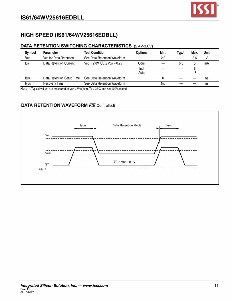
DATA RETENTION WAVEFORM (CE Controlled)
HIGH SPEED (IS61/64WV25616EDBLL)
DATA RETENTION SWITCHING CHARACTERISTICS (2.4V-3.6V) Symbol Parameter Test Condition Options Min. Typ.(1) Max. Unit Vdr VddforDataRetention SeeDataRetentionWaveform 2.0 — 3.6 V Idr DataRetentionCurrent Vdd = 2.0V, CE ≥ Vdd–0.2V Com. — 0.5 5 mA Ind. — — 6 Auto. 15 tsdr DataRetentionSetupTime SeeDataRetentionWaveform 0 — — ns trdr RecoveryTime SeeDataRetentionWaveform trc — — nsNote 1: TypicalvaluesaremeasuredatVdd = Vdr(min),Ta = 25oc and not 100% tested.
VDD
CE ≥ VDD - 0.2V
tSDR tRDR
VDR
CEGND
Data Retention Mode

12 Integrated Silicon Solution, Inc. — www.issi.comRev. A1
02/10/2017
IS61/64WV25616EDBLL
Automotive (A1) Range: -40°C to +85°C Speed (ns) Order Part No. Package
10 IS64WV25616EDBLL-10BA1 48miniBGA(6mmx8mm) IS64WV25616EDBLL-10BLA1 48miniBGA(6mmx8mm),Lead-free IS64WV25616EDBLL-10CTA1 TSOP(TypeII),CopperLeadframe IS64WV25616EDBLL-10CTLA1 TSOP(TypeII),Lead-free,CopperLeadframe
Automotive (A3) Range: -40°C to +125°C
Speed (ns) Order Part No. Package
10 IS64WV25616EDBLL-10BA3 48miniBGA(6mmx8mm) IS64WV25616EDBLL-10BLA3 48miniBGA(6mmx8mm),Lead-free IS64WV25616EDBLL-10CTA3 TSOP(TypeII),CopperLeadframe IS64WV25616EDBLL-10CTLA3 TSOP(TypeII),Lead-free,CopperLeadframe
ORDERING INFORMATION (HIGH SPEED)
Industrial Range: -40°C to +85°C Speed (ns) Order Part No. Package
8 IS61WV25616EDBLL-8BI 48miniBGA(6mmx8mm) IS61WV25616EDBLL-8BLI 48miniBGA(6mmx8mm),Lead-free IS61WV25616EDBLL-8TI TSOP(TypeII) IS61WV25616EDBLL-8TLI TSOP(TypeII),Lead-free
10 IS61WV25616EDBLL-10BI 48miniBGA(6mmx8mm) IS61WV25616EDBLL-10BLI 48miniBGA(6mmx8mm),Lead-free IS61WV25616EDBLL-10TI TSOP(TypeII) IS61WV25616EDBLL-10TLI TSOP(TypeII),Lead-free

Integrated Silicon Solution, Inc. — www.issi.com 13Rev. A102/10/2017
1
2
3
4
5
6
7
8
9
10
11
12
IS61/64WV25616EDBLL
2. D
IMEN
SIO
N D
AN
D E
1 D
O N
OT
INC
LUD
E M
OLD
PR
OTR
USI
ON
.3.
DIM
EN
SIO
N b
DO
ES
NO
T IN
CLU
DE
DA
MB
AR
PR
OTR
US
ION
/INTR
US
ION
.
1. C
ON
TRO
LLIN
G D
IME
NS
ION
: M
M
NO
TE :
Θ
Θ
06/0
4/20
08Pa
ckag
e O
utlin
e
14 Integrated Silicon Solution, Inc. — www.issi.comRev. A1
02/10/2017
IS61/64WV25616EDBLL
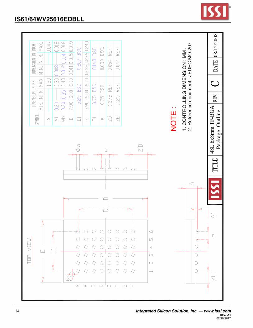
2. R
efer
ence
doc
umen
t : J
ED
EC
MO
-207
1. C
ON
TRO
LLIN
G D
IME
NS
ION
: M
M .
NO
TE :
08/1
2/20
08Pa
ckag
e O
utlin
e