IPC-2221
123
IPC-2221 Generic Standard on Printed Board Design IPC-2221 February 1998 Supersedes IPC-D-275 September 1991 The Institute for Interconnecting and Packaging Electronic Circuits A standard developed by the Institute for Interconnecting and Packaging Electronic Circuits 2215 Sanders Road Northbrook, Illinois 60062-6135 Tel Fax URL: 847 509.9700 847 509.9798 http://www.ipc.org
-
Upload
lamjed-whibi -
Category
Documents
-
view
2.576 -
download
195
Transcript of IPC-2221
IPC-2221
Generic Standard on
Printed Board Design
IPC-2221February 1998
Supersedes IPC-D-275September 1991
The Institute for
Interconnecting
and Packaging
Electronic Circuits
A standard developed by the Institute for Interconnectingand Packaging Electronic Circuits
2215 Sanders RoadNorthbrook, Illinois60062-6135
TelFaxURL:
847 509.9700847 509.9798http://www.ipc.org

Standardization In May 1995 the IPC’s Technical Activities Executive Committee adopted Prin-ciples of Standardization as a guiding principle of IPC’s standardization efforts.
Standards Should:• Show relationship to DFM & DFE• Minimize time to market• Contain simple (simplified) language• Just include spec information• Focus on end product performance• Include a feed back system on use and problems for future improvement
Standards Should Not:• Inhibit innovation• Increase time-to-market• Keep people out• Increase cycle time• Tell you how to make something• Contain anything that cannot be defended with data
Notice IPC Standards and Publications are designed to serve the public interest througheliminating misunderstandings between manufacturers and purchasers, facilitat-ing interchangeability and improvement of products, and assisting the pur-chaser in selecting and obtaining with minimum delay the proper product forhis particular need. Existence of such Standards and Publications shall notin any respect preclude any member or nonmember of IPC from manufacturingor selling products not conforming to such Standards and Publication, norshall the existence of such Standards and Publications preclude their voluntaryuse by those other than IPC members, whether the standard is to be usedeither domestically or internationally.
Recommended Standards and Publications are adopted by IPC without regard towhether their adoption may involve patents on articles, materials, or processes.By such action, IPC does not assume any liability to any patent owner, nordo they assume any obligation whatever to parties adopting the RecommendedStandard or Publication. Users are also wholly responsible for protectingthemselves against all claims of liabilities for patent infringement.
The material in this standard was developed by the IPC-D-275 Task Group(D-31b) of the Rigid Printed Board Committee (D-30) of the Institute forInterconnecting and Packaging Electronic Circuits.
Copyright © 1998 by the Institute for Interconnecting and Packaging Electronic Circuits. All rights reserved. Published 1998. Printed in theUnited States of America.
No part of this publication may be reproduced in any form, in an electronic retrieval system or otherwise, without the prior written permissionof the publisher.
IPC-2221
Generic Standard on
Printed Board Design
Developed by the IPC-D-275 Task Group (D-31b) of the Rigid PrintedBoard Committee (D-30) of the Institute for Interconnecting andPackaging Electronic Circuits
Users of this standard are encouraged to participate in the
development of future revisions.
Contact:
IPC2215 Sanders RoadNorthbrook, Illinois60062-6135Tel 847 509.9700Fax 847 509.9798
THE INSTITUTE FOR
INTERCONNECTING
AND PACKAGING
ELECTRONIC CIRCUITS
FOREWORD
This standard is intended to provide information on the generic requirements for organic printed board design. All aspectsand details of the design requirements are addressed to the extent that they can be applied to the broad spectrum of thosedesigns that use organic materials or organic materials in combination with inorganic materials (metal, glass, ceramic, etc.)to provide the structure for mounting and interconnecting electronic, electromechanical, and mechanical components. It iscrucial that a decision pertaining to the choice of product types be made as early as possible. Once a component mountingand interconnecting technology has been selected the user should obtain the sectional document that provides the specificfocus on the chosen technology.
It may be more effective to consider alternative printed board construction types for the product being designed. As anexample the application of a rigid-flex printed wiring board may be more cost or performance effective than using multipleprinted wiring boards, connectors and cables.
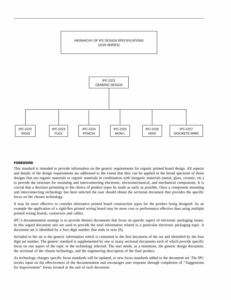
IPC’s documentation strategy is to provide distinct documents that focus on specific aspect of electronic packaging issues.In this regard document sets are used to provide the total information related to a particular electronic packaging topic. Adocument set is identified by a four digit number that ends in zero (0).
Included in the set is the generic information which is contained in the first document of the set and identified by the fourdigit set number. The generic standard is supplemented by one or many sectional documents each of which provide specificfocus on one aspect of the topic or the technology selected. The user needs, as a minimum, the generic design document,the sectional of the chosen technology, and the engineering description of the final product.
As technology changes specific focus standards will be updated, or new focus standards added to the document set. The IPCinvites input on the effectiveness of the documentation and encourages user response through completion of ‘‘Suggestionsfor Improvement’’ forms located at the end of each document.
HIERARCHY OF IPC DESIGN SPECIFICATIONS (2220 SERIES)
IPC-2222 RIGID
IPC-2223 FLEX
IPC-2224 PCMCIA
IPC-2225 MCM-L
IPC-2226 HDIS
IPC-2227 DISCRETE WIRE
IPC-2221 GENERIC DESIGN

AcknowledgmentAny Standard involving a complex technology draws material from a vast number of sources. While the principal membersof the IPC-D-275 Task Group (D-31b) of the Rigid Printed Board Committee (D-30) are shown below, it is not possible toinclude all of those who assisted in the evolution of this Standard. To each of them, the members of the IPC extend theirgratitude.
Rigid Printed BoardCommittee
IPC-D-275 Task Group(D-31b)
Technical Liaison of theIPC Board of Directors
ChairmanBob NevesMicrotek Lab
ChairmanLionel FullwoodWong’s Kong King Int’l
Ronald UnderwoodCircuit Center
IPC-D-275 Task Group
Richard Altenhofen, Motorola GSTGDaniel Arnold, EMD Associates Inc.Lance A. Auer, Hughes MissileSystems Company
Nanci J. Baggett, Printed CircuitResources
Steve Bakke, Alliant TechsystemsInc.
Karl J. Bates, Lucent TechnologiesRobert E. Beauchamp, LockheedMartin Missiles & Space
Frank Belisle, Sundstrand AerospaceDavid W. Bittle, Raytheon AircraftCompany
Daniel L. Botts, Hughes Training,Inc.
John Bourque, Shure Brothers Inc.Scott A. Bowles, Sovereign CircuitsInc.
Stephen G. Bradley, CALCorporation
Jim Brock, SCI Systems Inc.Ignatius Chong, CelesticaDavid J. Corbett, DSCCBrian Crowley, Hewlett PackardLaboratories
Georgia DeGrandis, ABB CeagPower Supplies Inc.
Yong Deng, Owens-CorningFiberglass Corp.
Michele J. DiFranza, The Mitre Corp.C. Don. Dupriest, Lockheed MartinVought Systems
Theodore Edwards, Honeywell Inc.Will J. Edwards, Lucent TechnologiesInc.
Werner Engelmaier, EngelmaierAssociates, Inc.
Thomas R. Etheridge, McDonnellDouglas Aerospace
Joe Fjelstad, Tessera Inc.Martin G. Freedman, Amp Inc.Lionel Fullwood, Wong’s Kong KingInt’l
Mahendra S. Gandhi, Hughes AircraftCo.
Paul Grande, Jr., U.S. NavyMichael R. Green, Lockheed MartinMissiles & Space
Lyle F. Harford, Texas InstrumentsInc.
Andrew J. Heidelberg, MicronCustom Mfg. Services Inc.
Ralph J. Hersey, Ralph Hersey &Associates
Phillip E. Hinton, Hinton -PWB-Engineering
Octavian Iordache, Circo Craft Co.Inc.
Don Jensen, Endicott Research GroupArturo J. Jordan, Pollak TrnsprtatnElectrnics Div
John A. Kelly, Motorola GSTGTherese Kokocinski, NorthropGrumman Corporation
Stephen Korchynsky, LockheedMartin Federal Systems
George T. Kotecki, NorthropGrumman Corporation
Thomas E. Kurtz, Hughes DefenseCommunications
Clifford H. Lamson, Harris Corp.Bonnie Lauch, Honeywell Inc.Stan C. Mackzum, Ericsson Inc.James F. Maguire, Boeing Defense &Space Group
David J. Malanchuk, Eastman KodakCo. KAD
Wesley R. Malewicz, SiemensMedical Systems Inc.
Susan Mansilla, Robisan LaboratoryInc.
Lester Mielczarek, CAE ElectronicsLtd.
Kelly J. Miller, CAE Electronics Ltd.John H. Morton, Lockheed MartinFederal Systems
Karl B. Mueller, Hughes Aircraft Co.Joseph L. Mulcahy, MethodeElectronics Inc. East
Benny Nilsson, Ericsson Telecom ABR. Bruce. Officer, Sanders, ALockheed Martin Co.
Scott S. Opperhauser, TraceLaboratories - East
John Papinko, Gulton Data SystemsRon Payne, Primex AerospaceRichard Peyton, Lockheed MartinAstronautics
Larry L. Puckett, Sandia NationalLabs Albuquerque
Paul J. Quinn, Lockheed MartinMissiles & Space
Kurt Ravenfeld, Lockheed MartinCorporation
Randy R. Reed, Merix CorporationBruce C. Rietdorf, Hughes DefenseCommunications
Jerald G. Rosser, Hughes MissileSystems Company
Vincent J. Ruggeri, RaytheonCompany
Don W. Rumps, Lucent TechnologiesInc.
Robert Russell, Texas InstrumentsInc.
Merlyn L. Seltzer, Hughes DelcoSystems Operations
Nusrat Sherali, IBM Corp.Lowell Sherman, DSCC
February 1998 IPC-2221
iii

Rae Shyne, Prototron Circuits Inc.Grant (Rick) W. Smedley, III, PrintedCircuit Resources
E. Lon. Smith, Lucent TechnologiesInc.
Joseph J. Sniezek, IBM Corp./Endicott Electronic Pa
William F. Spurny, AlliedSignalAerospace
Robert J. St. Pierre, New EnglandLaminates
Thomas K. Stewart, Speedy CircuitsGil Theroux, Honeywell Inc.Ronald E. Thompson, U.S. NavyMax E. Thorson, Compaq ComputerCorporation
Lutz E. Treutler, FachverbandElektronik Design
Robert Vanech, Northrop GrummanNorden Systems
Eric L. Vollmar, Methode ElectronicsInc.
Forrest L. Voss, RockwellInternational
Rich Warzecha, Advanced Flex Inc.Clark F. Webster, Computing DevicesInternational
David A. White, Input/Output Inc.
IPC-2221 February 1998
iv

Table of Contents
1.0 SCOPE .................................................................... 11.1 Purpose .............................................................. 1
1.2 Documentation Hierarchy ................................. 1
1.3 Presentation........................................................ 1
1.4 Interpretation...................................................... 1
1.5 Definition of Terms ........................................... 1
1.6 Classification of Products.................................. 1
1.6.1 Board Type ........................................................ 1
1.6.2 Performance Classes.......................................... 1
1.6.3 Producibility Level ............................................ 2
2.0 APPLICABLE DOCUMENTS ................................... 22.1 Institute for Interconnecting and
Packaging Electronic Circuits (IPC) ............... 2
2.2 Joint Industry Standards .................................. 3
2.3 Military .............................................................. 3
2.4 Federal ............................................................... 3
2.5 American Society for Testing andMaterials ............................................................ 3
2.6 Underwriters Labs ............................................. 3
2.7 IEEE................................................................... 3
2.8 ANSI .................................................................. 3
3.0 GENERAL REQUIREMENTS ................................... 3
3.1 Information Hierarchy....................................... 4
3.1.1 Order of Precedence.......................................... 4
3.2 Design Layout ................................................... 4
3.2.1 End-Product Requirements................................ 4
3.3 Schematic/Logic Diagram................................. 4
3.4 Parts List............................................................ 4
3.5 Test Requirement Considerations ..................... 4
3.5.1 Printed Board Assembly Testability.................. 6
3.5.2 Boundary Scan Testing...................................... 7
3.5.3 Functional Test Concern for PrintedBoard Assemblies .............................................. 7
3.5.4 In-Circuit Test Concerns for PrintedBoard Assemblies .............................................. 9
3.5.5 Mechanical....................................................... 11
3.5.6 Electrical .......................................................... 11
3.6 Layout Evaluation .......................................... 12
3.6.1 Board Layout Design ...................................... 12
3.6.2 Feasibility Density Evaluation ........................ 12
3.7 Performance Requirements ............................. 13
4.0 MATERIALS ............................................................ 14
4.1 Material Selection............................................ 14
4.1.1 Material Selection for Structural Strength...... 15
4.1.2 Material Selection for Electrical Properties ... 16
4.1.3 Material Selection for EnvironmentalProperties ......................................................... 16
4.2 Dielectric Base Materials (IncludingPrepregs and Adhesives) ................................. 16
4.2.1 Bonding Material............................................. 16
4.2.2 Adhesives......................................................... 16
4.2.3 Adhesive Films or Sheets ............................... 18
4.2.4 Electrically Conductive Adhesives ................. 18
4.2.5 Thermally Conductive/ElectricallyInsulating Adhesives........................................ 18
4.3 Laminate Materials.......................................... 19
4.3.1 Color Pigmentation.......................................... 19
4.3.2 Dielectric Thickness/Spacing .......................... 19
4.4 Conductive Materials ...................................... 19
4.4.1 Electroless Copper Plating .............................. 19
4.4.2 Semiconductive Coatings ................................ 19
4.4.3 Electrolytic Copper Plating............................. 19
4.4.4 Gold Plating..................................................... 19
4.4.5 Nickel Plating .................................................. 20
4.4.6 Tin/Lead Plating .............................................. 21
4.4.7 Solder Coating................................................. 21
4.4.8 Other Metallic Coatings for EdgeboardContacts ........................................................... 21
4.4.9 Metallic Foil/Film............................................ 21
4.4.10 Electronic Component Materials .................... 21
4.5 Organic Protective Coatings .......................... 22
4.5.1 Solder Resist (Solder Mask) Coatings............ 22
4.5.2 Conformal Coatings ........................................ 23
4.5.3 Tarnish Protective Coatings ............................ 23
4.6 Marking and Legends...................................... 23
4.6.1 ESD Considerations ........................................ 24
5.0 MECHANICAL/PHYSICAL PROPERTIES ............. 24
5.1 Fabrication Considerations.............................. 24
5.1.1 Bare Board Fabrication ................................... 24
5.2 Product/Board Configuration .......................... 24
5.2.1 Board Type ...................................................... 24
5.2.2 Board Size ....................................................... 24
5.2.3 Board Geometries (Size and Shape) ............. 24
5.2.4 Bow and Twist................................................. 25
5.2.5 Structural Strength........................................... 25
5.2.6 Composite (Constraining-core) Boards........... 25
5.2.7 Vibration Design.............................................. 27
5.3 Assembly Requirements ................................ 28
5.3.1 Mechanical Hardware Attachment.................. 28
5.3.2 Part Support ..................................................... 28
5.3.3 Assembly and Test .......................................... 28
February 1998 IPC-2221
v

5.4 Dimensioning Systems .................................... 29
5.4.1 Dimensions and Tolerances............................. 29
5.4.2 Component and Feature Location................... 29
5.4.3 Datum Features................................................ 30
6.0 ELECTRICAL PROPERTIES ................................ 31
6.1 Electrical Considerations................................. 31
6.1.1 Electrical Performance .................................... 31
6.1.2 Power Distribution Considerations ................. 31
6.1.3 Circuit Type Considerations............................ 33
6.2 Conductive Material Requirements ................ 35
6.3 Electrical Clearance......................................... 39
6.3.1 B1-Internal Conductors ................................... 39
6.3.2 B2-External Conductors, Uncoated, SeaLevel to 3050 m.............................................. 40
6.3.3 B3-External Conductors, Uncoated,Over 3050 m.................................................... 40
6.3.4 B4-External Conductors, with PermanentPolymer Coating (Any Elevation) .................. 40
6.3.5 A5-External Conductors, with ConformalCoating Over Assembly (Any Elevation)....... 40
6.3.6 A6-External Component Lead/Termination,Uncoated .......................................................... 40
6.3.7 A7-External Component Lead/Termination,with Conformal Coating (Any Elevation) ...... 40
6.4 Impedance Controls......................................... 40
6.4.1 Microstrip ........................................................ 40
6.4.2 Embedded Microstrip ...................................... 41
6.4.3 Stripline Properties .......................................... 41
6.4.4 Asymmetric Stripline Properties..................... 41
6.4.5 Capacitance Considerations ............................ 43
6.4.6 Inductance Considerations .............................. 43
7.0 THERMAL MANAGEMENT ................................... 44
7.1 Cooling Mechanisms....................................... 44
7.1.1 Conduction....................................................... 44
7.1.2 Radiation.......................................................... 45
7.1.3 Convection....................................................... 46
7.1.4 Altitude Effects................................................ 46
7.2 Heat Dissipation Considerations..................... 46
7.2.1 Individual Component Heat Dissipation ........ 46
7.2.2 Thermal Management Considerationsfor Board Heatsinks ........................................ 47
7.2.3 Assembly of Heatsinks to Boards................... 47
7.2.4 Special Design Considerations forSMT Board Heatsinks ..................................... 49
7.3 Heat Transfer Techniques................................ 49
7.3.1 Coefficient of Thermal Expansion (CTE)Characteristics.................................................. 49
7.3.2 Thermal Transfer ............................................. 49
7.3.3 Thermal Matching ........................................... 49
7.4 Thermal Design Reliability ............................. 50
8.0 COMPONENT AND ASSEMBLY ISSUES ........... 508.1 General Placement Requirements ................... 52
8.1.1 Automatic Assembly ....................................... 52
8.1.2 Component Placement..................................... 52
8.1.3 Orientation ....................................................... 53
8.1.4 Accessibility .................................................... 53
8.1.5 Design Envelope.............................................. 54
8.1.6 Component Body Centering............................ 54
8.1.7 Mounting Over Conductive Areas .................. 54
8.1.8 Clearances........................................................ 54
8.1.9 Physical Support.............................................. 55
8.1.10 Heat Dissipation .............................................. 56
8.1.11 Stress Relief..................................................... 56
8.2 General Attachment Requirements ................. 58
8.2.1 Through-Hole .................................................. 58
8.2.2 Surface Mounting ............................................ 58
8.2.3 Mixed Assemblies ........................................... 58
8.2.4 Soldering Considerations ................................ 58
8.2.5 Connectors and Interconnects ......................... 58
8.2.6 Fastening Hardware......................................... 59
8.2.7 Stiffeners .......................................................... 60
8.2.8 Lands for Flattened Round Leads .................. 61
8.2.9 Solder Terminals.............................................. 61
8.2.10 Eyelets.............................................................. 63
8.2.11 Special Wiring ................................................ 63
8.2.12 Heat Shrinkable Devices................................. 63
8.2.13 Bus Bar ............................................................ 64
8.2.14 Flexible Cable.................................................. 64
8.3 Through-Hole Requirements........................... 64
8.3.1 Leads Mounted in Through-Holes.................. 64
8.4 Standard Surface Mount Requirements .......... 68
8.4.1 Surface-Mounted Leaded Components........... 68
8.4.2 Flat-pack Components..................................... 68
8.4.3 Ribbon Lead Termination................................ 68
8.4.4 Round Lead Termination................................. 68
8.4.5 Component Lead Sockets................................ 68
8.5 Fine Pitch SMT (Peripherals) ......................... 69
8.6 Bare Die........................................................... 69
8.6.1 Wire Bond........................................................ 69
8.6.2 Flip Chip.......................................................... 69
8.6.3 Chip Scale........................................................ 69
8.7 Tape Automated Bonding................................ 69
8.8 Solderball ......................................................... 69
9.0 HOLES/INTERCONNECTIONS.............................. 70
9.1 General Requirements for Landswith Holes........................................................ 70
9.1.1 Land Requirements.......................................... 70
IPC-2221 February 1998
vi

9.1.2 Annular Ring Requirements............................ 70
9.1.3 Thermal Relief in Conductor Planes .............. 71
9.1.4 Lands for Flattened Round Leads .................. 71
9.2 Holes ............................................................... 71
9.2.1 Location ........................................................... 71
9.2.2 Hole Location Tolerances................................ 71
9.2.3 Quantity ........................................................... 71
9.2.4 Spacing of Adjacent Holes.............................. 71
9.2.5 Hole Pattern Variation ..................................... 72
9.2.6 Aspect Ratio .................................................... 72
9.2.7 Blind and Buried Vias..................................... 72
10.0 GENERAL CIRCUIT FEATUREREQUIREMENTS ................................................. 73
10.1 Conductor Characteristics ............................... 73
10.1.1 Conductor Width and Thickness..................... 73
10.1.2 Electrical Clearance......................................... 74
10.1.3 Conductor Routing .......................................... 74
10.1.4 Conductor Spacing .......................................... 74
10.1.5 Plating Thieves ................................................ 74
10.2 Land Characteristics ........................................ 74
10.2.1 Manufacturing Allowances.............................. 74
10.2.2 Lands for Surface Mounting........................... 74
10.2.3 Test Points ....................................................... 74
10.2.4 Orientation Symbols........................................ 74
10.3 Large Conductive Areas.................................. 75
11.0 DOCUMENTATION ............................................... 7511.1 Special Tooling................................................ 75
11.2 Layout .............................................................. 75
11.2.1 Viewing............................................................ 75
11.2.2 Accuracy and Scale......................................... 75
11.2.3 Layout Notes ................................................... 78
11.2.4 Automated-Layout Techniques........................ 78
11.3 Deviation Requirements .................................. 78
11.4 Phototool Considerations ................................ 78
12.0 QUALITY ASSURANCE ....................................... 7812.1 Conformance Test Specimen........................... 79
12.2 Material Quality Assurance............................. 79
12.3 Conformance Evaluations ............................... 79
12.3.1 Specimen Quantity and Location.................... 79
12.3.2 Specimen Identification................................... 79
12.3.3 General Specimen Requirements .................... 80
12.4 Individual Specimen Design ........................... 81
12.4.1 Specimen A and B (Plated HoleEvaluation)....................................................... 81
12.4.2 Specimen C (Plating Adhesion and SurfaceSolderability) ................................................... 81
12.4.3 Specimen D (Interconnection Resistanceand Continuity)................................................ 81
12.4.4 Specimen E and H (Insulation Resistance) .... 82
12.4.5 Registration Specimen..................................... 83
12.4.6 Specimen G (Solder Resist Adhesion) ........... 88
12.4.7 Specimen M (Optional)................................... 88
12.4.8 Specimen N (Optional) ................................... 88
12.4.9 Specimen S ...................................................... 88
12.4.10 Specimen T...................................................... 88
12.4.11 Process Control Test Specimen....................... 88
APPENDIX A ............................................................... 94
INDEX .......................................................................... 95
Figures
Figure 3-1 Test Land Free Area for Parts and OtherIntrusions ........................................................ 10
Figure 3-2 Test Land Free Area for Tall Parts ................. 10
Figure 3-3 Probing Test Lands......................................... 10
Figure 3-4 Example of usable area calculation, mm....... 13
Figure 3-5 Printed board density evaluation.................... 15
Figure 5-1 Example of printed board sizestandardization, mm ....................................... 26
Figure 5-2 Typical asymmetrical constraining-coreconfiguration ................................................... 27
Figure 5-3A Multilayer Metal Core Board with TwoSymmetrical Copper-Invar-CopperConstraining Cores ........................................ 27
Figure 5-3B Symmetrical Constraining Core Boardwith a Copper-Invar-Copper Center Core ...... 27
Figure 5-4 Advantages of positional tolerance overbilateral tolerance, mm................................... 29
Figure 5-5A Example of location of a pattern ofplated-through holes, mm............................... 31
Figure 5-5B Example of a pattern of tooling/mountingholes, mm....................................................... 31
Figure 5-5C Example of location of a conductor patternusing fiducials, mm......................................... 32
Figure 5-5D Example of printed board profile locationand tolerance, mm.......................................... 32
Figure 5-5E Example of a printed board drawingutilizing geometric dimensioning andtolerancing, mm.............................................. 33
Figure 5-6 Fiducial clearance requirements .................... 33
Figure 5-7 Fiducials, mm ................................................. 34
Figure 5-8 Example of connector key slot locationand tolerance, mm.......................................... 35
Figure 6-1 Voltage/ground distribution concepts ............. 36
Figure 6-2 Single reference edge routing ........................ 37
Figure 6-3 Circuit distribution ........................................... 37
Figure 6-4 Conductor thickness and width for internaland external layers ......................................... 38
Figure 6-5 Transmission line printed boardconstruction .................................................... 42
February 1998 IPC-2221
vii

Figure 6-6 Capacitance vs. conductor width anddielectric thickness for microstriplines, mm. ....................................................... 44
Figure 6-7 Capacitance vs. conductor width andspacing for striplines, mm. ............................. 45
Figure 6-8 Single conductor crossover ............................ 45
Figure 7-1 Component clearancerequirements for automatic componentinsertion on through hole technologyprinted board assemblies. (in.)....................... 48
Figure 7-2 Relative coefficient of thermal expansion(CTE) comparison .......................................... 51
Figure 8-1 Component orientation for boundariesand/or wave solder applications..................... 54
Figure 8-2 Component body centering ............................ 54
Figure 8-3 Axial-leaded component mounted overconductors ...................................................... 54
Figure 8-4 Uncoated board clearance ............................. 55
Figure 8-5 Clamp-mounted axial-leaded component....... 55
Figure 8-6 Adhesive-bonded axial-leaded component .... 55
Figure 8-7 Mounting with feet or standoffs ...................... 56
Figure 8-8 Heat dissipation examples ............................. 57
Figure 8-9 Lead bends..................................................... 57
Figure 8-10 Typical Lead configurations............................ 58
Figure 8-11 Board edge tolerancing .................................. 60
Figure 8-12 Lead-in chamfer configuration........................ 60
Figure 8-13 Typical keying arrangement ........................... 60
Figure 8-14 Two-part connector......................................... 61
Figure 8-15 Edge-board adapter connector....................... 61
Figure 8-16 Round or flattened (coined) lead jointdescription ...................................................... 62
Figure 8-17 Standoff terminal mounting, mm .................... 62
Figure 8-18 Dual hole configuration for interfacial andinterlayer terminal mountings ......................... 63
Figure 8-19 Partially clinched through-hole leads ............. 64
Figure 8-20 Dual in-line package (DIP) lead bends .......... 65
Figure 8-21 Solder in the lead bend radius ....................... 66
Figure 8-22 Two-lead radial-leaded components .............. 66
Figure 8-23 Radial two-lead component mounting, mm.... 66
Figure 8-24 Meniscus clearance, mm................................ 66
Figure 8-25 ‘‘TO’’ can radial-leaded component, mm........ 66
Figure 8-26 Perpendicular part mounting, mm.................. 67
Figure 8-27 Flat-packs and Quad Flat-packs .................... 67
Figure 8-28 Examples of configuration of ribbonleads for through-hole mountedflat-packs ........................................................ 67
Figure 8-29 Metal power packages with compliantleads ............................................................... 67
Figure 8-30 Metal power package with resilientspacers ........................................................... 67
Figure 8-31 Metal power package with non-compliantleads ............................................................... 67
Figure 8-32 Examples of flat-pack surface mounting ........ 69
Figure 8-33 Round or coined lead ..................................... 69
Figure 8-34 Configuration of ribbon leads for planarmounted flat-packs ......................................... 69
Figure 8-35 Heel mounting requirements .......................... 69
Figure 9-1 Examples of modified land shapes ................ 70
Figure 9-2 External annular ring ...................................... 71
Figure 9-3 Internal annular ring ....................................... 71
Figure 9-4 Typical thermal relief in planes....................... 72
Figure 10-1 Example of conductor beef-up orneck-down ...................................................... 74
Figure 10-2 Conductor optimization between lands .......... 75
Figure 10-3 Etched Conductor Characteristics.................. 76
Figure 11-1 Flow Chart of Printed Board Design/Fabrication Sequence..................................... 77
Figure 11-2 Multilayer Board Viewing................................ 78
Figure 11-3 Solder resist windows..................................... 78
Figure 12-1 Location of test circuitry ................................. 80
Figure 12-2 Test Specimen A and B, mm.......................... 81
Figure 12-3 Test Specimen A and B (conductor detail)..... 82
Figure 12-4 Specimen C, external layers only, mm .......... 82
Figure 12-5 Test Specimen D, mm.................................... 83
Figure 12-5cont. 10 Layer Example .......................................... 84
Figure 12-6 Example of a 10 layer specimen D,modified to include blind and buried vias....... 85
Figure 12-7 Test Specimen D for process control of4 layer boards................................................. 86
Figure 12-8 Specimen E, mm............................................ 86
Figure 12-9 Optional Specimen H, mm ............................. 87
Figure 12-10 Comb pattern examples ................................. 87
Figure 12-11 ‘‘Y’’ pattern for chip component cleanlinesstest pattern...................................................... 88
Figure 12-12 Test Specimen F, mm..................................... 89
Figure 12-13 Test Specimen R, mm.................................... 90
Figure 12-14 Worst-case hole/land relationship .................. 90
Figure 12-15 Test Specimen G, mm.................................... 91
Figure 12-16 Test Specimen M, surface mountingsolderability testing, mm................................. 91
Figure 12-17 Test Specimen N, surface mounting bondstrength and peel strength, mm ..................... 92
Figure 12-18 Test Specimen S, mm .................................... 92
Figure 12-19 Systematic path for implementation ofstatistical process control (SPC) .................... 93
Tables
Table 3-1 PWB Design/Performance TradeoffChecklist Considerations .................................. 5
Table 3-2 Component Grid Areas................................... 14
Table 4-1 Typical Properties of Common DielectricMaterials ......................................................... 16
Table 4-2 Environmental Properties of CommonDielectric Materials ......................................... 17
IPC-2221 February 1998
viii

Table 4-3 Final Finish, Surface Plating CoatingRequirements ................................................. 20
Table 4-4 Gold Plating Uses........................................... 20
Table 4-5 Copper Foil/Film Requirements...................... 21
Table 4-6 Metal Core Substrates.................................... 22
Table 4-7 Conformal Coating Functionality .................... 24
Table 5-1 Fabrication Considerations............................. 25
Table 5-2 Normal Assembly Equipment Limits............... 29
Table 6-1 Electrical Conductor Spacing ......................... 39
Table 6-2 Typical Relative Bulk DielectricConstant of Board Materials........................... 42
Table 7-1 Effects of Material Type on Conduction ......... 46
Table 7-2 Emissivity Ratings for Certain Materials ........ 46
Table 7-3 Board Heatsink Assembly Preferences.......... 49
Table 7-4 Comparative Reliability Matrix ComponentLead/Termination Attachment ......................... 50
Table 9-1 Minimum Standard Fabrication Allowancefor Interconnection Lands............................... 70
Table 9-2 Annular Rings (Minimum)............................... 71
Table 9-3 Minimum Hole Location Tolerance, dtp.......... 72
Table 9-4 Minimum Drilled Hole Size for Buried Vias.... 73
Table 9-5 Minimum Drilled Hole Size for Blind Vias ...... 73
Table 10-1 Internal Layer Foil Thickness AfterProcessing ...................................................... 73
Table 10-2 External Conductor Thickness AfterPlating............................................................. 73
Table 10-3 Conductor WidthTolerances for 46 µm Copper......................... 73
Table 12-1 Specimen Frequency Requirements .............. 80
February 1998 IPC-2221
ix

This Page Intentionally Left Blank
IPC-2221 February 1998
x
February 1998 IPC-2221
Generic Standard on Printed Board Design
thm-nii
ns
reda
ecnpo
nrermc-
tendo
c-
ofWheillede
hic
ire
ry.
s
aresi-
lar
-ry.ss
h-
ivere-g-enton-i-pri-
ellshed
ssgh
1.0 SCOPE
This standard establishes the generic requirements fordesign of organic printed boards and other forms of coponent mounting or interconnecting structures. The orgamaterials may be homogeneous, reinforced, or usedcombination with inorganic materials; the interconnectiomay be single, double, or multilayered.
1.1 Purpose The requirements contained herein aintended to establish design principles and recommentions thatshall be used in conjunction with the detailedrequirements of a specific interconnecting structure stional standard (see 1.2) to produce detailed desigintended to mount and attach passive and active comnents.
The components may be through-hole, surface mount, fipitch, ultra-fine pitch, array mounting or unpackaged badie. The materials may be any combination able to perfothe physical, thermal, environmental, and electronic funtion.
1.2 Documentation Hierarchy This standard identifiesthe generic physical design principles, and is supplemenby various sectional documents that provide details asharper focus on specific aspects of printed board technogy. Examples are:
IPC-2222 Rigid organic printed board structure designIPC-2223 Flexible printed board structure designIPC-2224 Organic, PC card format, printed board stru
ture designIPC-2225 Organic, MCM-L, printed board structure
designIPC-2226 High Density Interconnect (HDI) structure
designIPC-2227 Organic board design using discrete wiring
The list is a partial summary and is not inherently a partthis generic standard. The documents are a part of the PDesign Document Set which is identified as IPC-2220. Tnumber IPC-2220 is for ordering purposes only and winclude all documents which are a part of the set, whethreleased or in-process proposal format at the time the oris placed.
1.3 Presentation All dimensions and tolerances in thisstandard are expressed in SI (metric) units. Users of tand the corresponding performance and qualification spefications are expected to use metric dimensions.
1.4 Interpretation ‘‘ Shall,’’ the imperative form of theverb, is used throughout this standard whenever a requ
e
cn
-
-s-
e
d
l-
B
rr
si-
-
ment is intended to express a provision that is mandatoDeviation from a ‘‘shall’’ requirement may be considered ifsufficient data is supplied to justify the exception.
The words ‘‘should’’ and ‘‘may’’ are used whenever it isnecessary to express non-mandatory provisions. ‘‘Will’’ iused to express a declaration of purpose.
To assist the reader, the word ‘‘shall’’ is presented in boldcharacters.
1.5 Definition of Terms The definition of all terms usedhereinshall be as specified in IPC-T-50.
1.6 Classification of Products This standard recognizesthat rigid printed boards and printed board assembliessubject to classifications by intended end item use. Clasfication of producibility is related to complexity of thedesign and the precision required to produce the particuprinted board or printed board assembly.
Any producibility level or producibility design characteristic may be applied to any end-product equipment categoTherefore, a high-reliability product designated as Cla‘‘3’’ (see 1.6.2), could require level ‘‘A’’ design complexity(preferred producibility) for many of the attributes of theprinted board or printed board assembly (see 1.6.3).
1.6.1 Board Type This standard provides design infor-mation for different board types. Board types vary per tecnology and are thus classified in the design sectionals.
1.6.2 Performance Classes Three general end-productclasses have been established to reflect progressincreases in sophistication, functional performance requiments and testing/inspection frequency. It should be reconized that there may be an overlap of equipment betweclasses. The printed board user has the responsibilitydetermine the class to which his product belongs. The cotractshall specify the performance class required and indcate any exceptions to specific parameters, where approate.
Class 1 General Electronic ProductsIncludes consumerproducts, some computer and computer peripherals, as was general military hardware suitable for applicationwhere cosmetic imperfections are not important and tmajor requirement is function of the completed printeboard or printed board assembly.
Class 2 Dedicated Service Electronic ProductsIncludescommunications equipment, sophisticated businemachines, instruments and military equipment where hi
1

chin
reiti-usorarerse
l-no-oica
ahedat bthr-bllitytocr
o
tots21
d
ic
s
t
-
g
d
d
l
g
n
l
IPC-2221 February 1998
performance and extended life is required, and for whiuninterrupted service is desired but is not critical. Certacosmetic imperfections are allowed.
Class 3 High Reliability Electronic ProductsIncludes theequipment for commercial and military products whecontinued performance or performance on demand is crcal. Equipment downtime cannot be tolerated, and mfunction when required such as for life support items,critical weapons systems. Printed boards and printed boassemblies in this class are suitable for applications whhigh levels of assurance are required and service is estial.
1.6.3 Producibility Level When appropriate this standardwill provide three design complexity levels of features, toerances, measurements, assembly, testing of completioverification of the manufacturing process that reflect prgressive increases in sophistication of tooling, materialsprocessing and, therefore progressive increases in fabrtion cost. These levels are:
Level A General Design Complexity—PreferredLevel B Moderate Design Complexity—StandardLevel C High Design Complexity—Reduced
The producibility levels are not to be interpreted asdesign requirement, but a method of communicating tdegree of difficulty of a feature between design anfabrication/assembly facilities. The use of one level forspecific feature does not mean that other features musof the same level. Selection should always be based onminimum need, while recognizing that the precision, peformance, conductive pattern density, equipment, assemand testing requirements determine the design producibilevel. The numbers listed within the numerous tables arebe used as a guide in determining what the level of produibility will be for any feature. The specific requirement foany feature that must be controlled on the end itemshallbe specified on the master drawing of the printed boardthe printed board assembly drawing.
2.0 APPLICABLE DOCUMENTS
The following documents form a part of this documentthe extent specified herein. If a conflict of requiremenexist between IPC-2221 and those listed below, IPC-22takes precedence.
2.1 Institute for Interconnecting and Packaging Elec-tronic Circuits (IPC)1
IPC-A-22 UL Recognition Test Pattern
IPC-T-50 Terms and Definitions for Interconnecting anPackaging Electronic Circuits
2
t
den-
or
r-
ee
y
-
r
IPC-L-109 Specification for Resin Preimpregnated Fabr(Prepreg) for Multilayer Printed Boards
IPC-MF-150 Metal Foil for Printed Wiring Applications
IPC-CF-152 Composite Metallic Material Specification forPrinted Wiring Boards
IPC-FC-232 Adhesive Coated Dielectric Films for Use aCover Sheets for Flexible Printed Wiring
IPC-D-279 Design Guidelines for Reliable Surface MounTechnology Printed Board Assemblies
IPC-D-310 Guidelines for Phototool Generation and Measurement Techniques
IPC-D-317 Design Guidelines for Electronic PackaginUtilizing High-speed Techniques
IPC-D-322 Guidelines for Selecting Printed Wiring BoardSizes Using Standard Panel Sizes
IPC-D-325 Documentation Requirements for PrinteBoards
IPC-D-330 Design Guide Manual
IPC-D-350 Printed Board Description in Digital Form
IPC-D-356 Bare Substrate Electrical Test Data Format
IPC-D-422 Design Guide for Press Fit Rigid Printed BoarBackplanes
IPC-TM-650 Test Methods Manual
Method 2.4.22 Bow and Twist
IPC-ET-652 Guidelines and Requirements for ElectricaTesting of Unpopulated Printed Boards
IPC-CM-770 Printed Board Component Mounting
IPC-SM-780 Component Packaging and Interconnectinwith Emphasis on Surface Mounting
IPC-SM-782 Surface Mount Design and Land PatterStandard
IPC-SM-785 Guidelines for Accelerated Reliability Testingof Surface Mount Solder Attachments
IPC-MC-790 Guidelines for Multichip Module TechnologyUtilization
IPC-CC-830 Qualification and Performance of ElectricaInsulating Compound for Printed Board
1. The Institute for Interconnecting and Packaging Electronic Circuits, 2215 Sanders Road, Northbrook, IL 60062-6135

nt
fer
n
a
r-
y
r
d
r
n
)
c-
r-
d
n
y-
-
eior
alsl,il-ffof
February 1998 IPC-2221
IPC-SM-840 Qualification and Performance of PermanePolymer Coating (Solder Mask) for Printed Boards
IPC-2510 Series
IPC-2511 Generic Requirements for Implementation oProduct Manufacturing Description Data and TransfMethodology
IPC-2513 Drawing Methods for Manufacturing DataDescription (formerly IPC-D-351)
IPC-2514 Printed Board Manufacturing Data Descriptio(formerly IPC-D-350)
IPC-2515 Bare Board Product Electrical Testing DatDescription (formerly IPC-D-356)
IPC-2516 Assembled Board Product Manufacturing (fomerly IPC-D-355)
IPC-2518 Parts List Product Data Description (formerlIPC-D-354)
IPC-2615 Printed Board Dimensions and Tolerances
IPC-4101 Laminate/Prepreg Materials Standard foPrinted Boards
IPC-6011 Generic Performance Specification for PrinteBoards
IPC-6012 Qualification and Performance Specification foRigid Printed Boards
IPC-100002 Universal Drilling & Profile Master Drawing
IPC-100047 Composite Test Pattern Basic DimensioDrawing - Ten Layer
IPC-100103 Master Drawing for Capability Test Board(Ten Layer Multilayer Board without Blind or Buried Vias
SMC-TR-001 An Introduction to Tape Automated BondingFine Pitch Technology
2.2 Joint Industry Standards1
J-STD-001 Requirements for Soldered Electrical and Eletronic Assemblies
J-STD-003 Solderability Tests for Printed Boards
J-STD-005 Requirements for Soldering Pastes
J-STD-006 Requirements for Electronic Grade SoldeAlloys and Fluxed and Non-Fluxed Solid Solders for Electronic Soldering Applications
J-STD-012 Implementation of Flip Chip and Chip ScaleTechnology
J-STD-013 Implementation of Ball Grid Array and OtherHigh Density Technology
2.3 Military2
MIL-G-45204 Gold Plating (Electrodeposited)
2.4 Federal2
QQ-N-290 Nickel Plating (Electrodeposited)
QQ-A-250 Aluminum Alloy, Plate and Sheet
QQ-S-635 Steel
2.5 American Society for Testing and Materials3
ASTM-B-152 Copper Sheet, Strip and Rolled Bar
ASTM-B-579 Standard Specification for ElectrodepositeCoating of Tin-Lead Alloy (Solder Plate)
2.6 Underwriters Labs4
UL-746E Standard Polymeric Materials, Material used iPrinted Wiring Boards
2.7 IEEE5
IEEE 1149.1 Standard Test Access Port and BoundarScan Architecture
2.8 ANSI6
ANSI/EIA 471 Symbol and Label for Electrostatic Sensitive Devices
3.0 GENERAL REQUIREMENTS
The information contained in this section describes thgeneral parameters to be considered by all disciplines prto and during the design cycle.
Designing the physical features and selecting the materifor a printed wiring board involves balancing the electricamechanical and thermal performance as well as the reliabity, manufacturing and cost of the board. The tradeochecklist (see Table 3-1) identifies the probable effect
2. Application for copies should be addressed to Standardization Documents Order Desk, Building 4D, 700 Robbins Avenue, Philadelphia, PA 19111-50943. American Society for Testing and Materials, 100 Barr Habor Drive, West Conshohocken, PA 19428-29594. Underwriters Labs, 333 Pfngsten Road, Northbrook, IL 60062-20025. IEEE, 445 Hoes Lane, P.O. Box 1331, Piscataway, NJ 08855-13316. ANSI, 655 15th Street N.W., Suite 300, Washington, DC 20005-5794
3
hsoe
o
le
ldsleaee
rroid
nti
nhm
ooe
a
e
az
n
ns
.antignctor
er-edhene-theputer-to-
dem-
g.ingci-nd
rial
ses,a-c-)the
ci-al
a
beity
IPC-2221 February 1998
changing each of the physical features or materials. Titems in the checklist need to be considered if it is necesary to change a physical feature or material from onethe established rules. Cost can also be affected by thparameters as well as those in Table 5-1.
3.1 Information Hierarchy
3.1.1 Order of Precedence In the event of any conflictin the development of new designs, the following orderprecedenceshall prevail:
1. The procurement contract
2. The master drawing or assembly drawing (suppmented by an approved deviation list, if applicable)
3. This standard
4. Other applicable documents
3.2 Design Layout The layout generation process shouinclude a formal design review of layout details by amany affected disciplines within the company as possibincluding fabrication, assembly and testing. The approvof the layout by representatives of the affected disciplinwill ensure that these production-related factors have beconsidered in the design.
The success or failure of an interconnecting structudesign depends on many interrelated considerations. Fan end-product usage standpoint, the impact on the desby the following typical parameters should be considere
• Equipment environmental conditions, such as ambietemperature, heat generated by the components, vention, shock and vibration.
• If an assembly is to be maintainable and repairable, cosideration must be given to component/circuit density, tselection of board/conformal coating materials, and coponent placement for accessibility.
• Installation interface that may affect the size and locatiof mounting holes, connector locations, lead protrusilimitations, part placement, and the placement of brackand other hardware.
• Testing/fault location requirements that might affect component placement, conductor routing, connector contassignments, etc.
• Process allowances such as etch factor compensationconductor widths, spacings, land fabrication, etc. (sSection 5 and Section 9).
• Manufacturing limitations such as minimum etched fetures, minimum plating thickness, board shape and sietc.
• Coating and marking requirements.
• Assembly technology used, such as surface mouthrough hole, and mixed.
• Board performance class (see 1.6.2).
4
e-fse
f
-
,lsn
emgn.
tla-
-e-
nnts
-ct
fore
-e,
t,
• Materials selection (see Section 4).
• Producibility of the printed board assembly as it pertaito manufacturing equipment limitations.–Flexibility (Flexural) Requirements–Electrical/Electronic–Performance Requirements
• ESD sensitivity considerations
3.2.1 End-Product Requirements The end-productrequirementsshall be known prior to design start-upMaintenance and serviceability requirements are importfactors which need to be addressed during the desphase. Frequently, these factors affect layout and condurouting.
3.3 Schematic/Logic Diagram The initial schematic/logic diagram designates the electrical functions and intconnectivity to be provided to the designer for the printboard and its assembly. This schematic should define, wapplicable, critical circuit layout areas, shielding requirments, grounding and power distribution requirements,allocation of test points, and any preassigned input/outconnector locations. Schematic information may be genated as hard copy or computer data (manually or aumated).
3.4 Parts List A parts list is a tabulation of parts anmaterials used in the construction of a printed board assbly. All end item identifiable parts and materialsshall beidentified in the parts list or on the field of the drawinExcluded are those materials used in the manufacturprocess, but may include reference information; i.e., spefications pertinent to the manufacture of the assembly areference to the schematic/logic diagram.
All mechanical parts appearing on the assembly pictoshall be assigned an item number whichshall match theitem number assigned on the parts list.
Electrical components, such as capacitors, resistors, fuIC’s, transistors, etc.,shall be assigned reference designtors, (Ex. C5, CR2, F1, R15, U2, etc.). Assignment of eletrical reference designatorsshall be the same as (matchthose assignments given to the same components onLogic/schematic diagram.
It is advisable to group like items; e.g., resistors, capators, IC’s, etc., in some sort of ascending or numericorder.
The parts list may be handwritten, manually typed on tostandard format, or computer generated.
3.5 Test Requirement Considerations Normally, priorto starting a design, a testability review meeting shouldheld with fabrication, assembly, and testing. Testabil
February 1998 IPC-2221
Table 3-1 PWB Design/Performance Tradeoff Checklist Considerations 1
Physical Feature Class 2 Parameter
If Value of Physical Feature is Increased
Parameter is:Resulting Performance
or Reliability is:
Increased Decreased Enhanced Degraded
Dielectric Thickness toGround
EP Lateral Crosstalk X X
EP Vertical Crosstalk X X
EP Characteristic Impedance X X
MP Physical Size/Weight X X
Line Spacing EP Lateral Crosstalk X X
M/Y Electrical Isolation X X
Coupled Line Length EP Lateral Crosstalk X X
EP Vertical Crosstalk X X
Line Width EP Lateral Crosstalk X X
EP Vertical Crosstalk X X
EP Characteristic Impedance X DesignDriven
R Signal Conductor Integrity X X
M/Y Electrical Continuity X X
Dual Stripline EP Lateral Crosstalk X X
EP Vertical Crosstalk X X
EP Reflections X X
MP Physical Size/Weight X
M/Y Electrical Continuity X X
Line Thickness EP Lateral Crosstalk X X
R Signal Conductor Integrity X X
Vertical Line Spacing EP Vertical Crosstalk X X
Z0 of PWB vs. Z0 of Device EP Reflections X X
PTH Grid Spacing MP Physical Size/Weight X X
Signal Layer Quantity MP Physical Size/Weight X X
M/Y Layer-to-Layer Registration X X
Component I/O Pitch MP Physical Size/Weight X X
Board Thickness R PTH Integrity X X
M/Y PTH Plating Thickness X X
Copper Plating Thickness R PTH Integrity X X
Overplate (Nickel -Kevlaronly)
R PTH Integrity X X
Hole Diameter M/Y PTH Plating Thickness X X
Dielectric Thickness EP Lateral Crosstalk X X
EP Vertical Crosstalk X X
EP Characteristic Impedance X
MP Physical Size/Weight X X
R PTH Integrity X X
MP Flatness Stability X X
Insulation Resistance EP Lateral Crosstalk X X
EP Vertical Crosstalk X X
Dielectric Constant EP Characteristic Impedance X
Density Dielectric and Metal MP Physical Size/Weight X X
CTE (out-of-plane) R PTH Integrity X X
5

IPC-2221 February 1998
Table 3-1 PWB Design/Performance Tradeoff Checklist Considerations 1 (continued)
Physical Feature Class 2 Parameter
If Value of Physical Feature is Increased
Parameter is:Resulting Performance
or Reliability is:
Increased Decreased Enhanced Degraded
CTE (in-plane) R Solder Joint Integrity X X
R Signal Conductor Integrity X X
Resin Tg R PTH Integrity X X
R Solder Joint Integrity X X
Copper Ductility R PTH Integrity X X
R Signal Conductor Integrity X X
Copper Peel Strength R Solder Land Adhesion(Footprint)
X X
Dimensional Instability M/Y Layer-to-LayerMisregistration
X X
Mechanical FeatureClearances (Internal)
EP/MP/R Electrical Performance X X
1. How to read Table 3-1: As an example, the first row of the table indicates that if the dielectric thickness to ground is increased, the lateral crosstalk alsoincreases and the resultant performance of the PWB is degraded (because lateral crosstalk is not a desired property).
2. EP = Electrical Performance, MP = Mechanical Performance, R = Reliability, M/Y = Manufacturability/Yield
r--tet-
-t
di
ae-a-ulmesteee
sretsateetaeaarhi-e-ctt ia
andredgy.ofhyres
temtualire-edpro-wntheplehe
areederstestbyedrdrop-
inoardichem-allested
concerns, such as circuit visibility, density, operation, cicuit controllability, partitioning, and special test requirements and specifications are discussed as a part of thestrategy. See Appendix A for a checklist of design for tesability criteria.
During the design testability review meeting, tooling concepts are established, and determinations are made as tomost effective tool-cost versus board layout concept contions.
During the layout process, any circuit board changes thimpact the test program, or the test tooling, should immdiately be reported to the proper individuals for determintion as to the best compromise. The testing concept shodevelop approaches that can check the board for probleand also detect fault locations wherever possible. The tconcept and requirements should economically facilitathe detection, isolation, and correction of faults of thdesign verification, manufacturing, and field support of thprinted board assembly life cycle.
3.5.1 Printed Board Assembly Testability Design of aprinted board assembly for testability normally involvesystems level testability issues. In most applications, theare system level fault isolation and recovery requiremensuch as mean time to repair, percent up time, operthrough single faults, and maximum time to repair. To methe contractual requirements, the system design minclude testability features, and many times these same ftures can be used to increase testability at the printed boassembly level. The printed board assembly testability plosophy also needs to be compatible with the overall intgrations, testing and maintenance plans for the contraThe factory testers to be used, how integration and tesplanned, when printed board assemblies are conform
6
st
he-
t
ds,t
y-d
.sl
coated, the depot and field test equipment capabilitiespersonnel skill level are all factors that must be considewhen developing the printed board assembly test strateThe test philosophy may be different for different phasesthe program. For example, the first unit debug philosopmay be much different than the test philosophy for spawhen all the systems have already been shipped.
Before the PWB design starts, requirements for the systestability functions should be presented at the concepdesign review. These requirements and any derived requments should be partitioned down to the various printboard assemblies and documented. The system andgram level test criteria and how they are partitioned doto the printed board assembly requirements are beyondscope of this document. Appendix A provides an examof a checklist to be used in evaluating the testability of tdesign.
The two basic types of printed board assembly testfunctional test and in-circuit test. Functional testing is usto test the electrical design functionality. Functional testaccess the board under test through the connector,points, or bed-of-nails. The board is functionally testedapplying pre-determined stimuli (vectors) at the printboard assembly’s inputs while monitoring the printed boaassembly outputs to ensure that the design responds perly.
In-circuit testing is used to find manufacturing defectsprinted board assemblies. In-circuit testers access the bunder test through the use of a bed-of-nails fixture whmakes contact with each node on the printed board assbly. The printed board assembly is tested by exercisingthe parts on the board individually. In-circuit testing placless restrictions on the design. Conformal coated prin
giesaorriddongy
eet only-chof
uitu-ndaree
tlygi-
tesip’sfoenorin-st
ontoanhe
-icastfoto.aciaign
er,
thetherededtest
aryullnifi-
testanenth-lowntedr ane
heofni-icalol-onal
gnsthe
anbedis
n-ingonsreehe
ir-
if-itmu-one.
February 1998 IPC-2221
board assemblies and many Surface Mount Technolo(SMT) and mixed technology printed board assemblpresent bed-of-nails physical access problems which mprohibit the use of in-circuit testing. Primary concerns fin-circuit test are that the lands or pins (1) must be on g(for compatibility with the use of bed-of-nails fixture) an(2) should be accessible from the bottom side (a.k.a. ncomponent or solder side of through-hole technoloboards) of the printed board assembly.
Manufacturing Defects Analyzer (MDA) provide a lowcost alternative to the traditional in-circuit tester. Like thin-circuit tester, the MDA examines the construction of thprinted board assembly for defects. It performs a subsethe types of tests, mainly only tests for shorts and opefaults without power applied to the printed board assembFor high volume production with highly controlled manufacturing processes (i.e., Statistical Process Control teniques), the MDA may have application as a viable parta printed board assembly test strategy.
Vectorless Test is another low cost alternative to in-circtesting. Vectorless Test performs testing for finding manfacturing process-related pin faults for SMT boards adoes not require programming of test vectors. It ispowered-off measurement technique consisting of thbasic types of tests:
1. Analog Junction Test– DC current measurement teson unique pin pairs of the printed board assembusing the ESD protection diodes present on most dital and mixed signal device pins.
2. RF Induction Test– Magnetic induction is used to tesfor device faults utilizing the printed board assemblidevices protection diodes. This technique uses chpower and ground pins to make measurementsfinding solder opens on device signal paths, brokbond wires, and devices damaged by ESD. Parts increctly oriented can also be detected. Fixturing containg magnetic inducers are required for this type of te
3. Capacitive Coupling Test– This technique usescapacitive coupling to test for pin opens and does nrely on internal device circuitry but instead relies othe presence of the metallic lead frame of the devicetest the pins. Connectors and sockets, lead framescorrect polarity of capacitors can be tested using ttechnique.
3.5.2 Boundary Scan Testing As printed board assemblies become more dense with fine pitch devices, physaccess to printed board assembly nodes for in-circuit teing may not be possible. The boundary scan standardintegrated circuits (IEEE 1149.1) provides the meansperform virtual in-circuit testing to alleviate this problemBoundary scan architecture is a scan register approwhere, at the cost of a few I/O pins and the use of specscan registers in strategic locations throughout the des
y
y
-
fs.
-
r
-
t
d
l-r
hl,
the test problem can be simplified to testing of simplmostly combinational circuits.
In many applications, the inclusion of scan registers oninputs and outputs of the printed board assembly allowsboard to be tested while installed. If the circuit is mocomplex, additional sets of scan registers can be incluin the design to capture intermediate results and applyvectors to exercise portions of the design.
A full description of the standard access port and boundscan architecture can be found in IEEE 1149.1. The ftest access port capabilities are not needed to gain sigcant testability via the scan registers.
The decision to use boundary scan test as part of astrategy should consider the availability of boundary scparts and the return on investment for capital equipmand software tools required for implementing this test tecnique. Boundary scan testing can be conducted using acost PC-based tester which requires access to the priboard assembly under test through the edge connector oexisting functional, in-circuit, or hybrid tester that may badapted to perform boundary scan testing.
3.5.3 Functional Test Concern for Printed BoardAssemblies There are several concerns for designing tprinted board assembly for functional testability. The usetest connectors, problems with initialization and synchrozation, long counter chains, self diagnostics, and phystesting are topics which are discussed in detail in the flowing subsections and are not meant to be tutorialstestability but rather ideas of how to overcome typicfunctional testing problems.
3.5.3.1 Test Connectors Fault isolation on conformalcoated boards or most SMT and mixed technology desican be very difficult because of the lack of access tocircuitry on the board.
If strategic signals are brought out to a test connector orarea on the printed board where the signals can be pro(test points), fault isolation may be much improved. Thlowers the cost of detection, isolation and correction.
It is also possible to design the circuit so that a test conector can be used to stimulate the circuit (such as takover a data bus via the test connector) or disable function the printed board assembly (such as disabling a frunning oscillator and adding single step capability via ttest connector).
3.5.3.2 Initialization and Synchronization Some designsor portions of a design do not need any initialization ccuitry because the circuit will quickly cycle into itsintended function. Unfortunately, it is sometimes very dficult to synchronize the tester with this type of circubecause the tester would need to be programmed to stilate the circuit until a predetermined signature is foundthe outputs of the circuit. This can be difficult to achiev
7

w-ndo
inipte2)k;mto
tebn tis
erhaeteislagh
ststo
aithedlvrieplenybug-
allsaythce
thanteo
thetheede.
cked
it-
ksern
nddm-mebug
soingedthendpe-
icher,onryt istheed
anla-m-intnalforhetedtylsec-o bea
ofrnal
IPC-2221 February 1998
With relatively little difference in the design, initializationcapability can usually be designed into the circuitry alloing the printed board assembly to be quickly initialized athe circuit and the tester can follow the expected outputsthe printed board assembly.
Free running oscillators also present a problem in testbecause of the synchronization problem with the test equment. These problems can be overcome by (1) addingcircuitry to select a test clock instead of the oscillator; (removing the oscillator for test and injecting a test cloc(3) overriding the signal; or (4) designing the clock systeso that the clocking can be controlled via a test connecor test points.
3.5.3.3 Long Counter Chains Long counter chains in thedesign with signals used from many stages of the counchain present another testability problem. Testability canvery bad if there is no means to preset the counter chaidifferent values to facilitate testing of the logic thatdriven from the high order stages of the counter chain.
Testability is much improved if the counter chain is eithbroken into smaller counter chains (perhaps no more t10 stages) which can be individually controlled or if thcounter chain can be loaded via the test software. Thesoftware can then verify the operation of the logic thatdriven from the counter stages without wasting the simution and test time that would be required to clock throuthe complete counter chain.
3.5.3.4 Self Diagnostics Self diagnostics are sometimeimposed either contractually or via derived requiremenCareful consideration should be given to determine howimplement these requirements.
Many times a printed board assembly does not contfunctions that lend themselves to self diagnostics atprinted board assembly level but a small group of printboard assemblies, when taken as a unit, do lend themseto good diagnostics. For example, a complex Fast FouTransform (FFT) function may be spread across multiprinted board assemblies. It may be very difficult for aone printed board assembly to self diagnose a problemit may be very easy to design-in circuitry that self dianoses the whole FFT function.
The depth of self diagnostics that are needed is usudriven by the line replaceable unit (LRU) which variewith requirements. It may be an integrated circuit or it mbe a drawer of electronics depending on the contract,function of the design, or the system level maintenanphilosophy.
For self diagnostics at a printed board assembly level,printed board assembly is usually put into a test modethen the printed board assembly applies a known set ofinputs and compares the results with a stored set
8
f
g-st
r
reo
n
st
-
.
ne
esr
t
y
e
edstf
expected responses. If the results do not matchexpected responses, the printed board assembly signalstest equipment indicating the printed board assembly failthe self-test. There are many variations on this schemSome examples are:
1. The printed board assembly is placed in a feedbaloop with the results checked after a predeterminnumber of cycles.
2. A special test circuit or the Central Processor Un(CPU) applying the stimuli and comparing the signature of the responses against a known pattern.
3. The printed board assembly performing self-checwhen idling and then supplying the results to anoth(or diagnostic) printed board assembly for verificatioof the responses, etc.
3.5.3.5 Physical Test Concerns Printed board assemblyfunctional test equipment is usually very expensive arequires highly skilled personnel to operate. If printeboard assembly testability is poor, the printed board assebly test operation can be very expensive. There are sosimple physical considerations that can decrease the detime and therefore the overall test costs.
The orientation of polarized parts should be consistentthat the operator does not get confused with parts beoriented 180° out of phase with other parts on the printboard assembly. Non-polarized parts still need to havepin #1 identified so that the test operator knows which eto probe when guided probe software says to probe a scific pin.
Test connectors are much preferred over test points whrequire the use of test clips or test hook-up wires. Howevtest points such as riser leads are preferred over clippingto the lead of a part. If riser leads are used for temporatesting, such as determining a select-by-test resistor, isuggested that the risers remain after the installation ofselected component. This allows verification of the selectitem without re-fixturing the assembly.
Signals that are not accessible for probing (such as chappen with leadless parts) can greatly increase fault isotion problems. If scan registers are not used, it is recomended that every signal have a land or other test posomewhere on the printed board assembly where the sigcan be probed. It is also recommended that lands usedtest points be located on grid and placed so that all tprobing can be done from the secondary side of the prinboard assembly. If it is not feasible to provide capabilifor probing every signal, then (1) only the strategic signashould have special probing locations and (2) the test vtors need to be increased or other test techniques need tutilized to assign fault isolation to one component orsmall set of components.
Many faults are often due to shorts between the leadsadjacent parts, shorts between a part lead and an exte
twothenoofs tdto
talicaysusuplitya-teshee
ardignresresrethebeypx-allfixardantpeorfori-ch
,rrefacndor
an-Tthofn-th
ndgnletail
ilscte-ly-
iasseefora-rds
t onn aentf
notrdsts.g
of
ithds
n/theureint
dheh-heve
os-ore
ds.es.
ea.en
February 1998 IPC-2221
layer conductor on the printed board or shorts betweenprinted board conductors on the external layers ofprinted board. The physical design must consider thesemal manufacturing defects and not impair the isolationthe faults due to lack of access or inconvenient accessignals. As with design for in-circuit testability, probe patest points should be on grid to allow automated probingbe used in the future.
Partitioning of the design into functions, perhaps digiseparated from analog, is sometimes required for electrperformance. Testing concerns also are helped with phcal separation of dissimilar functions. Separation of not jthe circuitry but also the test connectors or at least groing the pins on the connectors can help improve testabiDesigns that mix digital design with high performance anlog design may require testing on two or more sets ofequipment. Separating the signals will not only help ttest fixturing but will help the operator in debugging thprinted board assembly.
As with in-circuit test fixturing, functional test fixturingcan have a significant cost impact. Normally a standboard size or only a few board sizes are used for all deson a program. Similarly one, or at most a few, test fixtuare typically used for a program. Generating test fixtucan be costly and debugging noise problems in the fixtuor tuning the fixtures to the tester can be expensive. Iftest fixturing is not adequately engineered, it may notpossible to accurately measure the board under test. Tcally much effort is expended in generating a few test fitures and it is expected that the fixtures will be used forthe printed board assembly designs. Therefore the testturing restrictions must be considered in the printed boassembly design. The fixturing restraints can be significSuch as (1) requiring ground and voltage supplies on scific connector pins, (2) limiting which pins can be used fhigh speed signals, (3) limiting which pins can be usedlow noise applications, (4) defining power switching limtations, (5) defining voltage and current limitations on eapin, etc.
3.5.4 In-Circuit Test Concerns for Printed BoardAssemblies In-circuit testing is used to find shortsopens, wrong parts, reversed parts, bad devices, incoassembly of printed board assemblies and other manuturing defects. In-circuit testing is neither meant to fimarginal parts nor to verify critical timing parametersother electrical design functions.
In-circuit testing of digital printed board assemblies cinvolve a process that is known as backdriving (see IPC50). Backdriving can also cause devices to oscillate andtester can have insufficient drive to bring a device outsaturation. Backdriving can be performed only for cotrolled periods of time, or the junction of the device (withe overdriven output) will overheat.
r-
o
li-t-.
t
s
s
i-
-
.-
ct-
-e
The two main concerns for designing the printed board aprinted board assembly for in-circuit testability are desifor compatibility with in-circuit test fixturing and electricadesign considerations. These topics are discussed in din the following subsections.
3.5.4.1 In-Circuit Test Fixtures In-circuit test fixturesare commonly called bed-of-nails fixtures. A bed-of-nafixture is a device with spring contact probes which contaeach node on the board under test. The following guidlines should be followed during printed board assemblayout to promote in-circuit testability in bed-of-nails fixtures:
1. The diameter of lands of plated-through holes and vused as test lands are a function of the hole size (9.1.1). The diameter of test lands used specificallyprobing should be no smaller than 0.9 mm. It is fesible to use 0.6 mm diameter test lands on boaunder 7700 mm2.
2. Clearances around test probe sites are dependenassembly processes. Probe sites should maintaiclearance equal to 80% of an adjacent componheight with a minimum of 0.6 mm and a maximum o5 mm (see Figure 3-1).
3. Part height on the probe side of the board mustexceed 5.7mm. Taller parts on this side of the boawill require cutouts in the test fixture. Test landshould be located 5 mm away from tall componenThis allows for test fixture profiling tolerances durintest fixture fabrication (see Figure 3-2).
4. No parts or test lands are to be located within 3 mmthe board edges.
5. All probe areas must be solder coated or covered wa conductive non-oxidizing coating. The test lanmust be free of solder resist and markings.
6. Probe the test lands or vias, not the terminatiocastellations of leadless surface mount parts orleads of leaded parts (see Figure 3-3). Contact presscan cause an open circuit or make a cold solder joappear good.
7. Avoid requiring probing of both sides of the printeboard. Use vias, to bring test points to one side, tbottom side (non-component or solder side of throughole technology printed board assemblies) of tboard. This allows for a reliable and less expensifixture.
8. Test lands should be on 2.5 mm hole centers, if psible, to allow the use of standard probes and a mreliable fixture.
9. Do not rely on edge connector fingers for test lanGold plated fingers are easily damaged by test prob
10. Distribute the test lands evenly over the board arWhen the test lands are not evenly distributed or wh
9
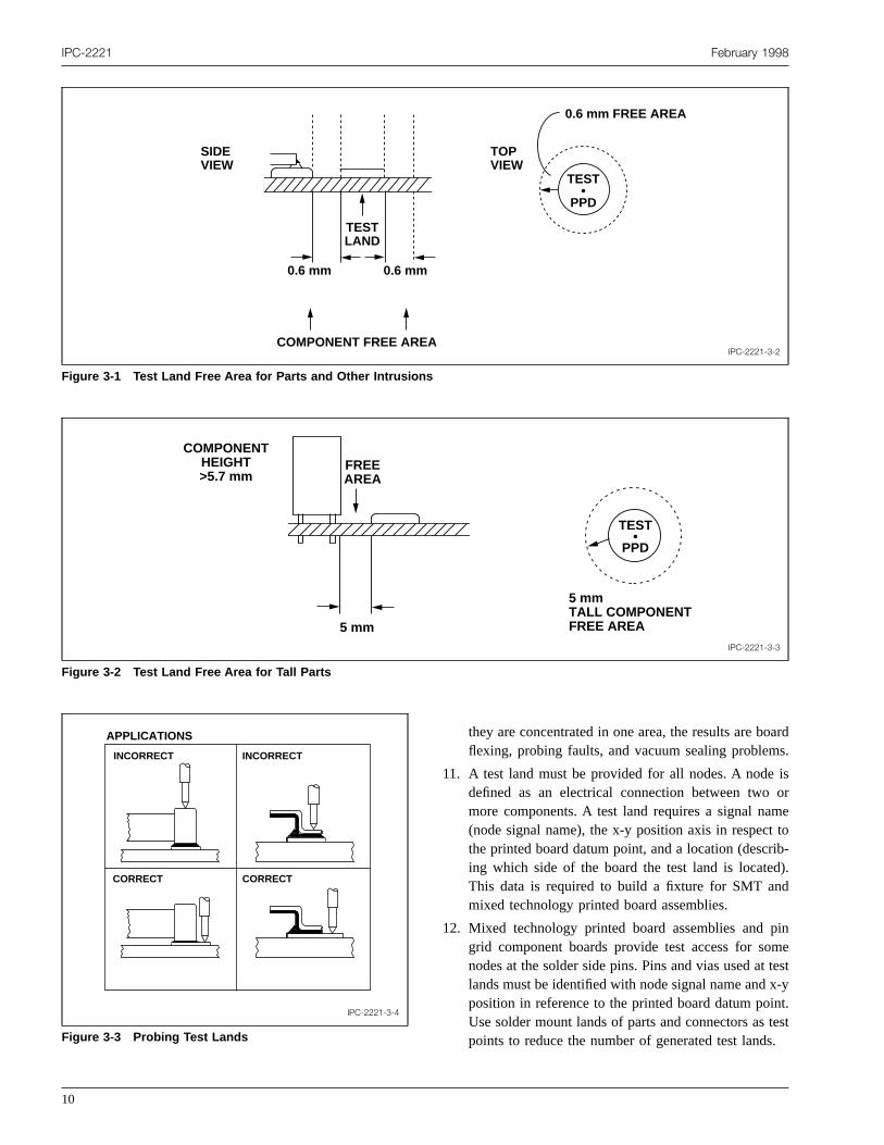
IPC-2221 February 1998
IPC-2221-3-2
Figure 3-1 Test Land Free Area for Parts and Other Intrusions
TEST •
PPD
0.6 mm
0.6 mm
TEST LAND
COMPONENT FREE AREA
SIDE VIEW
TOP VIEW
0.6 mm FREE AREA
IPC-2221-3-3
Figure 3-2 Test Land Free Area for Tall Parts
TEST •
PPD
5 mm TALL COMPONENT FREE AREA5 mm
COMPONENT HEIGHT >5.7 mm
FREE AREA
oards.
isormetoib-d).d
pinmetestx-ynt.tests.
IPC-2221-3-4
Figure 3-3 Probing Test Lands
APPLICATIONS
INCORRECT INCORRECT
CORRECTCORRECT
10
they are concentrated in one area, the results are bflexing, probing faults, and vacuum sealing problem
11. A test land must be provided for all nodes. A nodedefined as an electrical connection between twomore components. A test land requires a signal na(node signal name), the x-y position axis in respectthe printed board datum point, and a location (descring which side of the board the test land is locateThis data is required to build a fixture for SMT anmixed technology printed board assemblies.
12. Mixed technology printed board assemblies andgrid component boards provide test access for sonodes at the solder side pins. Pins and vias used atlands must be identified with node signal name andposition in reference to the printed board datum poiUse solder mount lands of parts and connectors aspoints to reduce the number of generated test land
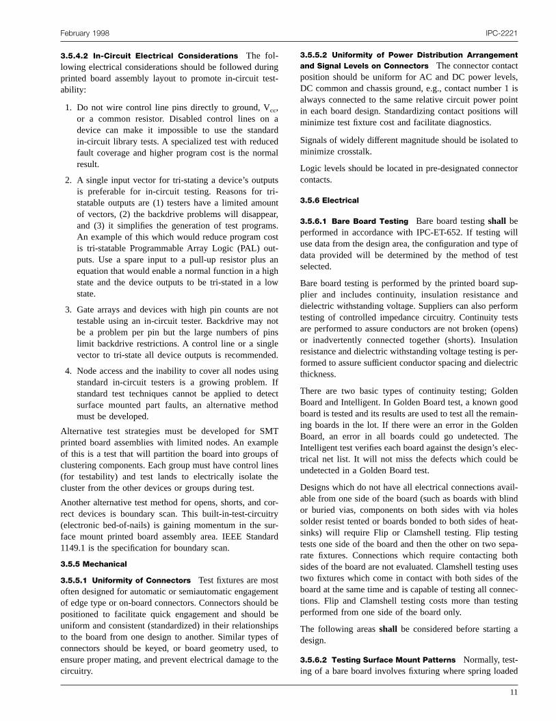
gst
arda
tsi-unr,sstt-anhow
noons
d
inIfteod
Tplefnee
oryr-a
ebbipo,th
ts,1 isintwill
to
tor
ille ofst
up-ndrmtsens)ioner-tric
enodain-enhelec-e
il-indleseat-gpa-thseseec-ing
a
ed
February 1998 IPC-2221
3.5.4.2 In-Circuit Electrical Considerations The fol-lowing electrical considerations should be followed durinprinted board assembly layout to promote in-circuit teability:
1. Do not wire control line pins directly to ground, Vcc,or a common resistor. Disabled control lines ondevice can make it impossible to use the standain-circuit library tests. A specialized test with reducefault coverage and higher program cost is the normresult.
2. A single input vector for tri-stating a device’s outpuis preferable for in-circuit testing. Reasons for trstatable outputs are (1) testers have a limited amoof vectors, (2) the backdrive problems will disappeaand (3) it simplifies the generation of test programAn example of this which would reduce program cois tri-statable Programmable Array Logic (PAL) ouputs. Use a spare input to a pull-up resistor plusequation that would enable a normal function in a higstate and the device outputs to be tri-stated in a lstate.
3. Gate arrays and devices with high pin counts aretestable using an in-circuit tester. Backdrive may nbe a problem per pin but the large numbers of pilimit backdrive restrictions. A control line or a singlevector to tri-state all device outputs is recommende
4. Node access and the inability to cover all nodes usstandard in-circuit testers is a growing problem.standard test techniques cannot be applied to desurface mounted part faults, an alternative methmust be developed.
Alternative test strategies must be developed for SMprinted board assemblies with limited nodes. An examof this is a test that will partition the board into groups oclustering components. Each group must have control li(for testability) and test lands to electrically isolate thcluster from the other devices or groups during test.
Another alternative test method for opens, shorts, and crect devices is boundary scan. This built-in-test-circuit(electronic bed-of-nails) is gaining momentum in the suface mount printed board assembly area. IEEE Stand1149.1 is the specification for boundary scan.
3.5.5 Mechanical
3.5.5.1 Uniformity of Connectors Test fixtures are mostoften designed for automatic or semiautomatic engagemof edge type or on-board connectors. Connectors shouldpositioned to facilitate quick engagement and shoulduniform and consistent (standardized) in their relationshto the board from one design to another. Similar typesconnectors should be keyed, or board geometry usedensure proper mating, and prevent electrical damage tocircuitry.
-
d
l
t
.
tt
.
g
ct
s
r-
rd
nteesftoe
3.5.5.2 Uniformity of Power Distribution Arrangementand Signal Levels on Connectors The connector contacposition should be uniform for AC and DC power levelDC common and chassis ground, e.g., contact numberalways connected to the same relative circuit power poin each board design. Standardizing contact positionsminimize test fixture cost and facilitate diagnostics.
Signals of widely different magnitude should be isolatedminimize crosstalk.
Logic levels should be located in pre-designated conneccontacts.
3.5.6 Electrical
3.5.6.1 Bare Board Testing Bare board testingshall beperformed in accordance with IPC-ET-652. If testing wuse data from the design area, the configuration and typdata provided will be determined by the method of teselected.
Bare board testing is performed by the printed board splier and includes continuity, insulation resistance adielectric withstanding voltage. Suppliers can also perfotesting of controlled impedance circuitry. Continuity tesare performed to assure conductors are not broken (opor inadvertently connected together (shorts). Insulatresistance and dielectric withstanding voltage testing is pformed to assure sufficient conductor spacing and dielecthickness.
There are two basic types of continuity testing; GoldBoard and Intelligent. In Golden Board test, a known goboard is tested and its results are used to test all the reming boards in the lot. If there were an error in the GoldBoard, an error in all boards could go undetected. TIntelligent test verifies each board against the design’s etrical net list. It will not miss the defects which could bundetected in a Golden Board test.
Designs which do not have all electrical connections avaable from one side of the board (such as boards with blor buried vias, components on both sides with via hosolder resist tented or boards bonded to both sides of hsinks) will require Flip or Clamshell testing. Flip testintests one side of the board and then the other on two serate fixtures. Connections which require contacting bosides of the board are not evaluated. Clamshell testing utwo fixtures which come in contact with both sides of thboard at the same time and is capable of testing all conntions. Flip and Clamshell testing costs more than testperformed from one side of the board only.
The following areasshall be considered before startingdesign.
3.5.6.2 Testing Surface Mount Patterns Normally, test-ing of a bare board involves fixturing where spring load
11

, thsugie
ndheomr-ed-caltheotreato
lyays-haint
ca
iteicireure
ndtedhaentedaheally
-o
stc-s,a
arehebeials
atedionandeuredi-
sibleing
wayce.
the
in
arts
nson
uirey ifand
tndthattail
andandbil-betheilluc-
ndd toable%l-hea
IPC-2221 February 1998
pins contact plated holes. On a surface mount patternends of the nets are typically not at holes but rather onface mount lands. There are at least two different stratefor performing testing:
A. Contact the via which is connected to the land avisually inspect to ensure continuity from the via to tland. Vias can be designed such that they are on a cmon grid which will reduce the need for special fixtuing for each part number. The barrels of the platthrough holes that are used for internal electriconnectivity should not be subject to probing unlessforce is very low and the point of the probe will ndamage the barrel. These barrels can crack or bfree from the land on the internal layer if subjectedmechanical stresses.
B. Test to the land itself. This approach will probabrequire special fixturing since surface mount lands mnot all be on a grid. Additionally, computer design sytems may place the end-of-net point at a via rather tthe land which may require adjustment of test polocations.
3.5.6.3 Testing of Paired Printed Boards Laminated to aCore At least two approaches are available for electritest:
A. Test the top and bottom of the laminated composprinted board separately. If there are plated holes whprovide a side-to-side interconnection, they will requa manual electrical test or visual inspection to enshole continuity.
B. Use a clam shell type fixture where both the top abottom of the composite printed board can be testogether. The use of the first approach will require tthe electrical test data be provided in two parts. Whnetworks have terminations on both sides of the prinboard, the electrical test data should be split intoleast two parts with the end of net occurring at tside-to-side interconnect. ‘‘Self learn’’ testing fromknown good board will provide the data automaticain the above format.
3.5.6.4 Point of Origin Electrical test and numerical control data should have a common origin point for easeconstructing electrical test fixtures.
3.5.6.5 Test Points When required by the design, tepoints for probingshall be provided as part of the condutor pattern andshall be identified on the drawing set. Viawide conductors, or component lead mounting lands mbe considered as probe points provided that sufficientis available for probing and maintaining the integrity of tvia, conductor, or component lead mounting joint. Propoints must be free of nonconductive coating matersuch as solder resist or conformal coating.
12
er-s
-
k
n
l
h
t
t
f
ya
3.6 Layout Evaluation
3.6.1 Board Layout Design The design layout from oneboard design to another should be such that designareas are identified by function, i.e., power supply sectconfined to one area, analog circuits to another section,logic circuits to another, etc. This will help to minimizcrosstalk, simplify bare board and assembly test fixtdesign, and facilitate troubleshooting diagnostics. In adtion, the design should:
• Ensure that components have all testable points accesfrom the secondary side of the board to facilitate probwith single-sided test fixtures.
• Have feed-throughs and component holes placed afrom board edges to allow adequate test fixture clearan
• Require the board be laid out on a grid which matchesdesign team testing concept.
• Allow provision for isolating parts of the circuit to facili-tate testing and diagnostics.
• Where practical, group test points and jumper pointsthe same physical location on the board.
• Consider high-cost components for socketing so that pcan be easily replaced.
• Provide optic targets (fiducials) for surface mount desigto allow the use of optic positioning and visual inspectiequipment and methods (see 5.4.3).
Surface mounted components and their patterns reqspecial consideration for test probe access, especiallcomponents are mounted on both sides of the boardhave very high lead counts.
3.6.1.1 Layout Concepts The printed board layoudepicts the physical size and location of all electronic amechanical components, and the routing of conductorselectrically interconnect the components in sufficient deto allow the preparation of documentation and artwork.
3.6.2 Feasibility Density Evaluation After approveddocuments for schematic/logic diagrams, parts lists,end-product and testing requirements are provided,before the actual drawing of the layout is begun, a feasiity density evaluation should be made. This shouldbased on the maximum size of all parts required byparts list and the total space they and their lands wrequire on the board, exclusive of interconnection condtor routing.
The total board geometry required for this mounting atermination of the components should then be comparethe total usable board area for this purpose. Reasonmaximum values for this ratio are 70% for Level A, 80for Level B, and 90% for Level C. Component density vaues higher than these will be a cause for concern. Tlower these values are, the easier it will be to designcost-effective functional board.

ard
mo-fole-nentsoutsp alineut-totnd
nperlyr-tshisofare
aly,
nd
February 1998 IPC-2221
Figure 3-4 provides the usable board area for the standized board sizes recommended in Figure 5-1.
Table 3-2 gives the area (in 0.5 mm grid elements) a coponent will occupy on the board for a variety of compnents. As an example, the 14 lead dual in-line packagethrough-hole technology occupies a total of 84.0 grid ements. The package outline that encloses the compoand land pattern has a grid matrix of 20 x 42 grid elemeon 0.5 mm centers. The 20 grid elements establish anline dimension of 10 mm while the 42 grid elemenaccount for 21 mm. This component area would use uportion of the board usable area. The component outdoes not include grid elements for conductor routing oside the land area. Total component area compared tousable area provides the conductor routing availability athus the density percentage.
��
-
-
r
nt
t-
al
An alternative method of feasibility density evaluatioexpresses board density in units of square centimetersequivalent SOIC. A 16-pin SOIC occupies approximateone cm2 of board area. Figure 3-5 shows a table for detemining the SOIC equivalent for a variety of componenand the total SOIC equivalents used on the board. Tnumber is then divided into the total square centimetersusable board area. Reasonable maximum density values0.55 cm2 per SOIC for Level A, 0.50 for Level B, and 0.45for Level C. Density values can increase with additioncircuit layers. Also, when using surface mount technologthe potential usable board area is theoretically doubled.
3.7 Performance Requirements Finished printed boardsshall meet the performance requirements of IPC-6011 aits applicable sectional standard.
Board Size(Fig. 5-1)
Overall Dimensions Usable Dimensions Usable Area
Height, mm Width, mm Height, mm Width, mm mm 2 Grid Elements0.5 mm Grid
cm2
A1 80
60
65
50
3200 12800 32
B1 170 155 7700 30800 77
C1 260 245 12200 48800 122
D1 350 335 16700 66800 167
A2 80
120
65
110
7100 28400 71
B2 170 155 17000 68000 170
C2 260 245 26900 107600 269
D2 350 335 36800 147200 368
A3 80
180
65
170
11000 44000 110
B3 170 155 26300 105200 263
C3 260 245 41600 166400 416
D3 350 335 56900 227600 569
A4 80
240
65
230
14900 59600 149
B4 170 155 35600 142400 356
C4 260 245 56300 225200 563
D4 350 335 77000 308000 770
Figure 3-4 Example of usable area calculation, mm (Usable area determination includes clearance allowance foredge-board connector area, board guides, and board extractor)
Usable Area
5.0 TYP
5.0 TYP
10.0 TYP
5.0 TYP
Tooling Holes
0/0 FiducialConnector Area
IPC-2221-3-5
13

IPC-2221 February 1998
Table 3-2 Component Grid Areas
Component Description Type 1Number of Grid Elements 2
0.5 mm Grid
D07 (without stress relief loop) THT 6 x 24 144
D07 (with stress relief loop) THT 6 x 28 168
T05 THT 20 x 20 400
T024 THT 10 x 10 100
CK05 THT 6 x 12 72
CM05, 13000pF THT 20 x 44 880
CM06, 400pF THT 12 x 26 312
RC07 THT 6 x 20 120
RC20 THT 10 x 26 260
RN60 THT 10 x 30 300
CQFP-10 T090 SMT 16 x 12 192
CQFP-28 SMT 34 x 34 1156
CQFP-144 SMT 68 x 68 4624
3216 (1206) SMT 4 x 10 40
4564 (1825) SMT 14 x 12 168
6032 SMT 8 x 18 144
DIP-14 THT 20 x 42 840
DIP-14 SMT 22 x 42 924
DIP-24 SMT 22 x 60 1320
DIP-24L SMT 26 x 64 1664
SOD87/MLL-41 SMT 6 x 14 84
SOT23 SMT 8 x 8 64
SOT89 SMT 12 x 10 120
SOT143 SMT 8 x 8 64
SQFP 7x7-40 SMT 22 x 22 484
SOIC-20W SMT 28 x 24 672
SOIC-36X SMT 48 x 24 1152
TSOP 10x20 SMT 22 x 44 968
SOJ 26/350 SMT 24 x 34 8161THT = Through-Hole Technology, SMT = Surface Mount Technology2Grid area includes physical component outlines and land areas. It does not include space for conductor routing.
saringireenicanebet
er-temest
of
4.0 MATERIALS4.1 Material Selection A designer of printed boards haseveral material choices to consider, ranging from standto highly sophisticated and specialized. When specifymaterials, the designer must first determine what requments the printed board must meet. These requireminclude temperature (soldering and operating), electrproperties, interconnections (soldered components, contors), structural strength, and circuit density. It shouldnoted that increased levels of sophistication may leadincreased material and processing costs.
When constructing a composite from materials with diffent temperature characteristics, the maximum end-useperature allowable must be limited to that of the lowrated material.
14
d
-tslc-
o
-
Other items that may be important in the comparisonvarious materials include:
Resin Formula,Flame Resistance,Thermal Stability,Structural Strength,Electrical Properties,Flexural Strength,Maximum Continuous Safe Operating Temperature,Glass Transition Temperature (Tg),Reinforcing Sheet Material,Nonstandard Sizes and Tolerances,Machinability or Punchability,Coefficients of Thermal Expansion (CTE),Dimensional Stability, andOverall Thickness Tolerances.

February 1998 IPC-2221
IPC-275-5-3
Figure 3-5 Printed board density evaluation
PRINTED BOARD DENSITY EVALUATION
DESCRIPTION: SOICs per square centimeter
Date of issue
No.
Revised
Comp. name # of comp. or IC equiv Comments
others (specify)
Total IC equivalent
Total board area
Usable board area
(X)
(X)
=
=
Devel. by Date App'd by Date
cm2
cm2
Usable board areaDesign criteria
Sheet 1 of 1
Analog Digital
Etch & Spac.
PWB & GYD Sz
/
/
8 SOIC .50
14 SOIC 1.00
16 SOIC 1.00
16L SOIC 1.00
20 SOIC 1.25
24 SOIC 1.50
28 SOIC 1.75
18 PLCC 1.13
18L PLCC 1.13
20 PLCC 1.25
28 PLCC 1.75
44 PLCC 2.75
52 PLCC 3.25
68 PLCC 4.25
84 PLCC 5.25
SOT 23 0.19
SOT 89 0.19
SOMC 1401 1.00
SOMC 1601 1.00
2012 (0805) 0.13
3216 (1206) 0.13
3225 (1210) 0.13
4564 (1812) 0.13
MLL 34 0.13
MLL 41 0.13
r-et,
dticer-
4.1.1 Material Selection for Structural Strength Thefirst design step in the selection of a laminate is to thooughly define the service requirements that must be mi.e., environment, vibration, ‘‘G’’ loadings, shock (impact)physical and electrical requirements.
,
The choice of laminate should be made from standarstructures to avoid costly and time consuming proof-outasks. Several laminates may be candidates, and the choshould be optimized to obtain the best balance of propeties.
15
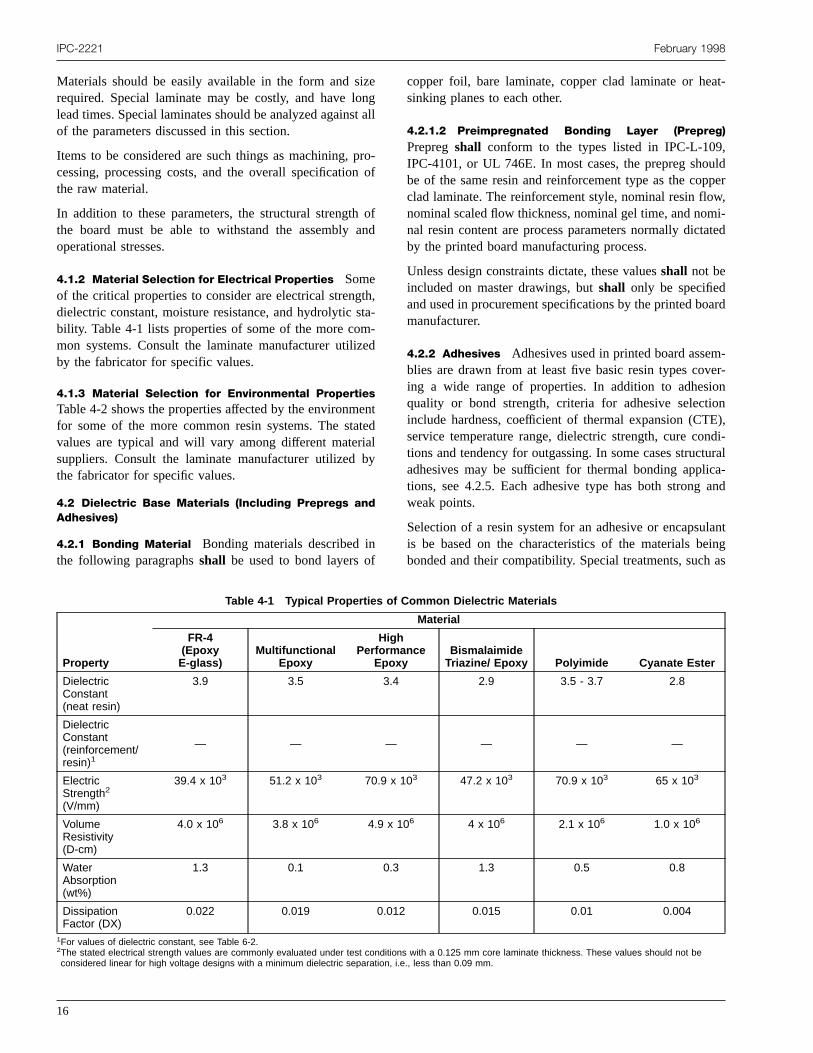
izengt a
pron o
oand
th,ta-ed
enteialby
f
at-
,uldpperw,i-
ated
ard
m-er-ononE),ndi-turalca-and
lantingas
IPC-2221 February 1998
Materials should be easily available in the form and srequired. Special laminate may be costly, and have lolead times. Special laminates should be analyzed againsof the parameters discussed in this section.
Items to be considered are such things as machining,cessing, processing costs, and the overall specificatiothe raw material.
In addition to these parameters, the structural strengththe board must be able to withstand the assemblyoperational stresses.
4.1.2 Material Selection for Electrical Properties Someof the critical properties to consider are electrical strengdielectric constant, moisture resistance, and hydrolytic sbility. Table 4-1 lists properties of some of the more common systems. Consult the laminate manufacturer utilizby the fabricator for specific values.
4.1.3 Material Selection for Environmental PropertiesTable 4-2 shows the properties affected by the environmfor some of the more common resin systems. The stavalues are typical and will vary among different matersuppliers. Consult the laminate manufacturer utilizedthe fabricator for specific values.
4.2 Dielectric Base Materials (Including Prepregs andAdhesives)
4.2.1 Bonding Material Bonding materials described inthe following paragraphsshall be used to bond layers o
16
ll
-f
f
-
td
copper foil, bare laminate, copper clad laminate or hesinking planes to each other.
4.2.1.2 Preimpregnated Bonding Layer (Prepreg)Prepregshall conform to the types listed in IPC-L-109IPC-4101, or UL 746E. In most cases, the prepreg shobe of the same resin and reinforcement type as the coclad laminate. The reinforcement style, nominal resin flonominal scaled flow thickness, nominal gel time, and nomnal resin content are process parameters normally dictby the printed board manufacturing process.
Unless design constraints dictate, these valuesshall not beincluded on master drawings, butshall only be specifiedand used in procurement specifications by the printed bomanufacturer.
4.2.2 Adhesives Adhesives used in printed board asseblies are drawn from at least five basic resin types coving a wide range of properties. In addition to adhesiquality or bond strength, criteria for adhesive selectiinclude hardness, coefficient of thermal expansion (CTservice temperature range, dielectric strength, cure cotions and tendency for outgassing. In some cases strucadhesives may be sufficient for thermal bonding applitions, see 4.2.5. Each adhesive type has both strongweak points.
Selection of a resin system for an adhesive or encapsuis be based on the characteristics of the materials bebonded and their compatibility. Special treatments, such
Table 4-1 Typical Properties of Common Dielectric Materials
Property
Material
FR-4(EpoxyE-glass)
MultifunctionalEpoxy
HighPerformance
EpoxyBismalaimideTriazine/ Epoxy Polyimide Cyanate Ester
DielectricConstant(neat resin)
3.9 3.5 3.4 2.9 3.5 - 3.7 2.8
DielectricConstant(reinforcement/resin)1
— — — — — —
ElectricStrength2
(V/mm)
39.4 x 10³ 51.2 x 10³ 70.9 x 10³ 47.2 x 10³ 70.9 x 10³ 65 x 103
VolumeResistivity(D-cm)
4.0 x 10⁶ 3.8 x 10⁶ 4.9 x 10⁶ 4 x 10⁶ 2.1 x 10⁶ 1.0 x 10⁶
WaterAbsorption(wt%)
1.3 0.1 0.3 1.3 0.5 0.8
DissipationFactor (DX)
0.022 0.019 0.012 0.015 0.01 0.004
1For values of dielectric constant, see Table 6-2.2The stated electrical strength values are commonly evaluated under test conditions with a 0.125 mm core laminate thickness. These values should not beconsidered linear for high voltage designs with a minimum dielectric separation, i.e., less than 0.09 mm.

February 1998 IPC-2221
Table 4-2 Environmental Properties of Common Dielectric Materials
Environmental Property
Material
FR-4(EpoxyE-glass)
MultifunctionalEpoxy
(E-glass)
HighPerformance
Epoxy(E-glass)
BismalaimideTriazine/Epoxy
Polyimide(E-glass)
CyanateEster
Thermal Expansionxy-plane (ppm/°C)
16 - 19 14 - 18 14 - 18 z15 8 - 18 z15
Thermal Expansion z-axisbelow Tg
3 (ppm/°C)50 - 85 44 - 80 z44 z70 35 - 70 81
Glass TransitionTemp. Tg (°C)
110 - 140 130 -160 165 - 190 175 - 200 220 - 280 180 - 260
Flexural Modulus(x 1010 Pa)
Fill1
Warp21.861.20
1.862.07
1.932.20
2.072.41
2.692.89
2.072.20
Tensile Strength(x 108 Pa)
Fill1
Warp24.134.82
4.134.48
4.135.24
3.934.27
4.825.51
3.454.13
1 Fill - yarns that are woven in a crosswise direction of the fabric.2 Warp (cloth) - yarns that are woven in the lengthwise direction of the fabric.3 Z-axis expansion above Tg can be as much as four times greater. For FR-4 it is 240-390 ppm. Contact supplier for specific values of the other materials.
telsueoncals
bags.
endgevethrendd,iodie-r
ynanec
ndhanedaltsn-otsedsed
blelsasicaltain
ness.to
ition
inrialsofcom-pingelyaltela--
primers or activators, may be required to suitably activasurfaces for bonding. The selection process should aconsider the exact purpose of the adhesive bond and itsenvironment. Fungus inert materials are also a considation. Not all adhesives are suitable for direct application or near electronic products due to either their chemior dielectric properties. Incorrect selection of materiamay result in product degradation or failure.
In actual application, most adhesive needs canaddressed by a few carefully selected materials. Storand shelf life limitations apply to most of these material
4.2.2.1 Epoxies Epoxy resin formulations are among thmost versatile adhesives for electrical insulating amechanical bonding applications. They offer a wide ranof physical and electrical properties, including adhesiand cohesive strengths, hardness, chemical resistance,mal conductivity and thermal vacuum stability. They aalso available with a wide range of cure methods atimes. A thorough review of the material is warrantebased on its intended use. Thermal coefficient of expansand glass transition temperatures should be considereaddition to other properties to preclude problems. Epoxare available with a variety of modifiers, fillers and reinforcements for specific applications and extended tempeture ranges.
4.2.2.2 Silicone Elastomers Silicone elastomers aregenerally noted for being resilient materials with vergoodelectrical and mechanical properties at ambient aextreme temperatures. Several curing methods are avable, including moisture, metallic salts and others. Silicoresins which evolve acetic acid should be avoided in ele
oser-
l
ee
er-
nins
a-
dil-
-
tronic applications. Bond strength, tensile strength, ahardness properties tend to be considerably lower tepoxies. Silicones will swell and dissolve with prolongexposure to some chemicals. Some of the metallic scuring silicones will react with TFE, PTFE materials. Coformal coatings, other than silicones, generally will nadhere to cured silicone materials. Silicones are often uas a cushioning overcoat for articles which will be encain hard potting compounds later.
A number of high purity grades of silicones are availawhich offer good thermal vacuum stability. Silicone geare also available, which offer enhanced propertiesencapsulants. These materials generally require physrestraint, such as a potting cup or enclosure to maintheir form, once applied.
4.2.2.3 Acrylics Acrylic resins generally provide rapidcures, good electrical and adhesive properties and hardChemical resistance and thermal vacuum stability tendbe considerably lower than the epoxies. The glass transtemperature of these materials also tends to be low.
4.2.2.4 Polyurethanes Polyurethanes are availablealmost as many variations as the epoxies. These mategenerally offer toughness, high elasticity, a wide rangehardness, and good adhesion. Some of the urethanepounds are outstanding as vibration and shock dammaterials. Moisture and chemical resistance is relativhigh, but varies with the individual product. Thermvacuum stability will also vary by the individual producformulation. Many of the urethanes can be used in a rtively thick application as a local vibration damping compound.
17

d
neeinh
tnrevn
si-dnl
ar
srfered
-eethdasmy
na-
n.e
sine-n-a-henra-s-
-ser
er-toni-ure
ssis-msn.s
ordpts-ing
by-d,
n
ds.woone
IPC-2221 February 1998
4.2.2.5 Specialized Acrylate-Based Adhesives Thiscategory includes the cyanoacrylates (instant cure) ananaerobic adhesives (cure without air). The cyanoacrylateform strong bonds within seconds without catalysts wheonly a trace amount of moisture is present on a surfacThe anaerobic adhesives cure in the absence of oxygwhen a peroxide additive can be decomposed by certatransition metal ions. Both adhesive types can give higinitial bond strengths which may be beneficial for wirestaking and temporary bonding applications. The instancure adhesives generally have poor impact resistance aare susceptible to degradation from exposure to moistuand temperatures over 82°C. The anaerobic adhesives hathe capability of withstanding higher temperatures but calose strength with prolonged exposure to chemicals.
4.2.2.6 Other Adhesives Many other types and forms ofadhesives are available, including polyesters, polyamidepolyimides, rubber resins, vinyl, hot melts, pressure senstive, etc. Where they are used is determined by the neeof the design and its performance requirements. Selectioof specialized items, such as chip bond adhesives, shoube done in conjunction with the using facility, in order toensure full compatibility of the equipment and process.
4.2.3 Adhesive Films or Sheets Adhesive films orsheets used for bonding heatsinks, stiffeners, etc., orinsulators, are generally in accordance with IPC-FC-232 oMIL-S-13949.
Film type adhesives find many uses in laminated structureThe ability to pre-cut a film adhesive to fit given shapes odimensions is a distinct advantage in the fabrication osome laminated parts. Epoxy based film adhesives providvery good bond strength but require elevated temperatucure. Film adhesives are commonly used to bond boarheatsinks to printed boards.
Through-hole technology (THT) printed boards and heatsinks may be bonded together with a dry epoxy sheet adhsive to improve heat transfer or resist vibration. Thesadhesives consist of an epoxy impregnated glass clowhich is cut to the heatsink configuration, assemblebetween printed board and heatsink, then cured with heand pressure. The cured adhesive is strong and resivibration, temperature extremes, and solvents. 0.1 mshould be adequate for most applications; if necessarspecify two thicknesses.
4.2.4 Electrically Conductive Adhesives This class ofadhesives consists, generally, of a conductive filler, such agraphite (carbon) or silver embedded in a polymeric resiadhesive system. Bonding strength of these materials cbe compromised by the filler loading to achieve conductivity. Volume resistivity, a measure of the electrically con-ductive property of the material, may be varied over a
18
s
.n
d
e
,
s
d
s
.
-
tts
,
s
n
range of values consistent with the intended applicatioThis is accomplished by the type of filler used and thloading.
Epoxies, silicone elastomers and urethanes are the resystems commonly used to formulate conductive adhsives. The strongest bonds are generally achieved with coductive epoxy, silicone elastomers follow with urethanesclose third. Cure conditions and filler content have a pronounced effect upon tensile strength of these materials. Tchoice of conductive adhesive for a particular applicatioshould consider the strength of bond, the service tempeture, the effect of CTE on the bond and the volume resitivity or conductivity required.
4.2.5 Thermally Conductive/Electrically InsulatingAdhesives Thermally conductive adhesives are filled versions of epoxy, silicone, urethane and some acrylic bamaterials. The filler is normally dried aluminum oxide omagnesium oxide powder.
4.2.5.1 Epoxies The epoxies offer the greatest bondstrength and best solvent resistance along with good thmal conductivity and electrical resistance. As with mostwo part systems, the choice of catalyst has an impactcure conditions and ultimately could affect the glass transtion temperature since it is somewhat dependent upon cconditions.
4.2.5.2 Silicone Elastomers The silicone elastomers arecharacterized by relatively low bond strengths and lerigidity (lower hardness) than epoxies. They are less restant to solvent attack than epoxy and are two part systewith variable other properties dependent upon formulatioThermal conductivity and electrical resistance propertieare good.
Silicone elastomers may be obtained as humidity curingheat curing, the latter offering accelerated cure with applieheat. They cure well in contact with most materials excebutyl and chlorinated rubbers, some RTV silicone elatomers and residues of some curing agents. Some bondapplications may require a primer.
4.2.5.3 Urethanes Urethanes can be varied through awide range of hardness, tensile and electrical propertiesvarying the proportions of curing agent to resin. Consistency can be varied from a soft, rubbery state to a harrigid condition by this method. The latitude for formulationoptimization over a range of application conditions is aadvantage offered by the filled urethanes.
The urethanes are characterized by relatively low bonstrengths and less rigidity (lower hardness) than epoxieThey are less resistant to solvent attack than epoxy; are tpart systems with variable other properties dependent upformulation. Thermal conductivity and electrical resistancproperties are good.
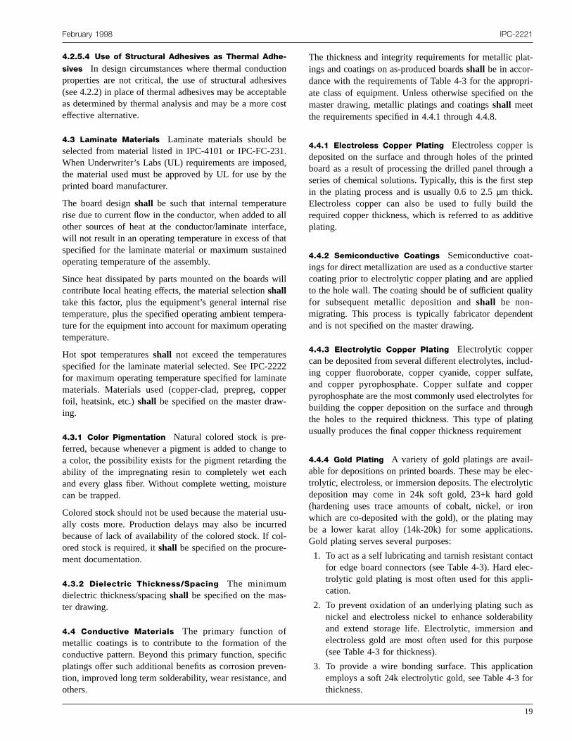
tioivtac
e31edth
reaacthane
w
risein
es2atpw-
-gethchur
urreol--
-
heifiean
lat-
pri-the
isintedgh atepick.theitive
t-arterliedlity
ent
rlud-fate,ppers forughtingnt
l-elec-yticoldironayns.
tactlec-li-
asilityndose
ionfor
February 1998 IPC-2221
4.2.5.4 Use of Structural Adhesives as Thermal Adhe-
sives In design circumstances where thermal conducproperties are not critical, the use of structural adhes(see 4.2.2) in place of thermal adhesives may be accepas determined by thermal analysis and may be a moreeffective alternative.
4.3 Laminate Materials Laminate materials should bselected from material listed in IPC-4101 or IPC-FC-2When Underwriter’s Labs (UL) requirements are imposthe material used must be approved by UL for use byprinted board manufacturer.
The board designshall be such that internal temperaturise due to current flow in the conductor, when added toother sources of heat at the conductor/laminate interfwill not result in an operating temperature in excess ofspecified for the laminate material or maximum sustaioperating temperature of the assembly.
Since heat dissipated by parts mounted on the boardscontribute local heating effects, the material selectionshalltake this factor, plus the equipment’s general internaltemperature, plus the specified operating ambient tempture for the equipment into account for maximum operattemperature.
Hot spot temperaturesshall not exceed the temperaturspecified for the laminate material selected. See IPC-2for maximum operating temperature specified for laminmaterials. Materials used (copper-clad, prepreg, copfoil, heatsink, etc.)shall be specified on the master draing.
4.3.1 Color Pigmentation Natural colored stock is preferred, because whenever a pigment is added to chana color, the possibility exists for the pigment retardingability of the impregnating resin to completely wet eaand every glass fiber. Without complete wetting, moistcan be trapped.
Colored stock should not be used because the materialally costs more. Production delays may also be incubecause of lack of availability of the colored stock. If cored stock is required, itshall be specified on the procurement documentation.
4.3.2 Dielectric Thickness/Spacing The minimumdielectric thickness/spacingshall be specified on the master drawing.
4.4 Conductive Materials The primary function ofmetallic coatings is to contribute to the formation of tconductive pattern. Beyond this primary function, specplatings offer such additional benefits as corrosion prevtion, improved long term solderability, wear resistance,others.
nesbleost
.,e
lle,td
ill
era-g
22eer
toe
e
su-d
cn-d
The thickness and integrity requirements for metallic pings and coatings on as-produced boardsshall be in accor-dance with the requirements of Table 4-3 for the approate class of equipment. Unless otherwise specified onmaster drawing, metallic platings and coatingsshall meetthe requirements specified in 4.4.1 through 4.4.8.
4.4.1 Electroless Copper Plating Electroless copperdeposited on the surface and through holes of the prboard as a result of processing the drilled panel throuseries of chemical solutions. Typically, this is the first sin the plating process and is usually 0.6 to 2.5 µm thElectroless copper can also be used to fully buildrequired copper thickness, which is referred to as addplating.
4.4.2 Semiconductive Coatings Semiconductive coaings for direct metallization are used as a conductive stcoating prior to electrolytic copper plating and are appto the hole wall. The coating should be of sufficient quafor subsequent metallic deposition andshall be non-migrating. This process is typically fabricator dependand is not specified on the master drawing.
4.4.3 Electrolytic Copper Plating Electrolytic coppecan be deposited from several different electrolytes, incing copper fluoroborate, copper cyanide, copper suland copper pyrophosphate. Copper sulfate and copyrophosphate are the most commonly used electrolytebuilding the copper deposition on the surface and throthe holes to the required thickness. This type of plausually produces the final copper thickness requireme
4.4.4 Gold Plating A variety of gold platings are avaiable for depositions on printed boards. These may betrolytic, electroless, or immersion deposits. The electroldeposition may come in 24k soft gold, 23+k hard g(hardening uses trace amounts of cobalt, nickel, orwhich are co-deposited with the gold), or the plating mbe a lower karat alloy (14k-20k) for some applicatioGold plating serves several purposes:
1. To act as a self lubricating and tarnish resistant confor edge board connectors (see Table 4-3). Hard etrolytic gold plating is most often used for this appcation.
2. To prevent oxidation of an underlying plating suchnickel and electroless nickel to enhance solderaband extend storage life. Electrolytic, immersion aelectroless gold are most often used for this purp(see Table 4-3 for thickness).
3. To provide a wire bonding surface. This applicatemploys a soft 24k electrolytic gold, see Table 4-3thickness.
19

IPC-2221 February 1998
Table 4-3 Final Finish, Surface Plating Coating Requirements*
Finish Class 1 Class 2 Class 3
Gold (min) for edge-boardconnectors and areas not to besoldered
0.8 µm 0.8 µm 1.3 µm
Gold (max) on areas to be soldered 0.8 µm 0.8 µm 0.8 µm
Gold (min) on areas to be wirebonded (ultrasonic)
0.05 µm 0.05 µm 0.15 µm
Gold (min) on areas to be wirebonded (thermosonic)
0.3 µm 0.3 µm 0.8 µm
Nickel (min) for edgeboardconnectors
2.0 µm 2.5 µm 2.5 µm
Nickel (min) barrier to preventformation of copper-tincompounds**
1.0 µm 1.3 µm 1.3 µm
Electroless Nickel 2.5 - 5.0 µm
Immersion Gold 0.08 - 0.23 µm
Unfused tin-lead (min) 8.0 µm 8.0 µm 8.0 µm
Fused tin-lead or Solder Coat Coverage and solderable Coverage and solderable Coverage and solderable
Solder Coat over Bare Copper Coverage and solderable Coverage and solderable Coverage and solderable
Organic Solderability Preservative Solderable Solderable Solderable
Bare Copper None None None
Surface and Holes
Copper* (Avg. minimum) 20 µm 20 µm 25 µm
Min. thin areas*** 18 µm 18 µm 20 µm
Blind Vias
Copper (Avg. minimum) 20 µm 20 µm 25 µm
Min. thin area 18 µm 18 µm 20 µm
Buried Vias
Copper (Avg. minimum) 13 µm 15 µm 15 µm
Min. thin area 11 µm 13 µm 13 µm
*Copper plating thickness applies to surfaces and hole walls.**Nickel platings used under the tin-lead or solder coating for high temperature operating environments act as a barrier to prevent the formation of copper-tincompounds.
***For Class 3 boards having a drilled hole diameter <0.35 mm and having an aspect ratio >3.5:1, the minimum thin area copper plating in the hole shall be 25µm
oneµm
ica-
asdeesldb
us
-erold;serm-nd
4. To provide an electrically conductive surfaceprinted wiring boards when electrically conductivadhesives are used. A minimum thickness of 0.25is recommended.
5. To act as an etch resist during printed board fabrtion. A minimum thickness of 0.13 µm is recommended.
Electrolytically deposited gold is often specifiedrequired to meet MIL-G-45204 with the type and graselected to satisfy the different applications. A low-strnickel or electroless nickelshall be used between the gooverplating and the basis metal when gold finish is toused for electrical or wire bonding.
Table 4-4 will help clarify some of the uses for the varioalloys.
20
-
s
e
4.4.5 Nickel Plating Nickel plating serves a dual function in contact plating: 1) It provides an anvil effect undthe gold providing an essential extra hardness to the g2) It is an effective barrier layer (when its thicknesexceeds 2.5 µm) which prevents the diffusion of coppinto gold. This diffusion process can result in a room teperature alloying of the gold, degrading the electrical acorrosion resistance characteristics of the contact.
Table 4-4 Gold Plating Uses
MinimumPurity
KnoopHardness Contacts
WireBonding Soldering
99.0 130-200 S C* C**
99.0 90 max NR S C**
S - Suitable use NR - Not recommended C - Conditional use* May be used, but will depend on type of wire bonding being used. RunTest prior to wire bonding.
** More than 0.8 µm gold on boards or leads may cause embrittled solderjoints.
th
tcic8.igonreraceitality
ghno
ts
-
dndl oal
edn
so
foinelityter
er
ir-i
g
ce
l-igidForer
entbeF-
tan-iald
ur-ntdis-ableriedto
February 1998 IPC-2221
All electrolytically deposited nickel platingshall be low-stress and conform to QQ-N-290, Class 2, except thatthicknessshall be as specified in Table 4-3.
4.4.6 Tin/Lead Plating Tin/Lead Plating is applied in thesubtractive fabrication process to provide a copper eresist and a solderable coating, when required. Typthickness sufficient for etch resist on 2 oz. copper isµm, but it is a fabrication process parameter, not a desrequirement. The electrodeposit is generally fused byof several techniques (hot oil immersion, infrared exposuexposure to hot vapors or inert liquids). The fusing opetion results in the formation of a true alloy on the surfaand in the through holes of the printed board. Fusingrequired unless the unfused option is selected to mainflatness. It also promotes improved long-term solderabi
Tin lead plating does not apply to buried plated-throuholes which are internal to the printed board and doextend to the surface.
Tin-lead platingshall meet the composition requiremenof ASTM-B-579.
4.4.6.1 Tin Plating Tin Plating is applied in the subtractive fabrication process to provide a copper etch resist.
4.4.7 Solder Coating Solder coating is generally applieby immersing the printed board into molten solder aremoving the excess by blowing hot, pressurized air, oivapors over the surface of the printed board in a specidesigned machine.
Solder coating does not apply to buried or tented platthrough holes which are internal to the printed board ado not extend to the surface.
Unless otherwise specified on the master drawing, theder used for solder coatingshall be in accordance withJ-STD-006. Solder coating thickness may be specifiedparticular applications. The performance of solder coatis evaluated, not by a mechanical thickness measurembut by the ability of the printed board to pass solderabitesting per J-STD-003 (see Table 4-3). The user hasresponsibility to determine if steam aging, prior to soldability testing, is required.
4.4.8 Other Metallic Coatings for Edgeboard ContactsInaddition to the coatings cited previously, there are sevother options that the designer may want to consider:
• Rhodium - a low resistance contact coating for flush ccuits, switches or where a high number of insertionsexpected. Expense has precluded its general use.
• Tin/Nickel Alloy- an abrasion resistant coating.
• Palladium/Nickel Alloy- a low resistance contact coatinMay be particularly useful for flush circuits.
e
hal0ne,-
sin.
t
rly
-d
l-
rgnt,
he-
al
s
.
• Electroless Nickel and Immersion Gold- a low resistancontact coating suitable for low number of insertions.
4.4.9 Metallic Foil/Film
4.4.9.1 Copper Foil There are two types of copper foiavailable: (W) - wrought (or rolled), and (ED) - electrodeposited. There are also several copper foil grades. For rboards, electrodeposited copper foil is generally used.flexible boards, wrought foil is generally used. Whichevtype is used, the copper foilshall conform to the require-ments of IPC-MF-150.
The thickness of starting copper conductorsshall be asdefined in Table 4-5 for the appropriate class of equipm(a reduction in copper thickness of inner layers mayexpected after processing). See Appendix A of IPC-M150 for details of foil properties.
4.4.9.2 Copper Film Copper filmshall be in accordancewith Table 4-5.
4.4.9.3 Other Foils/Film When other foils or films(nickel, aluminum, etc.) are used, their characteristicsshallbe specified on the master drawing.
4.4.9.4 Metal Core Substrates Substrates for metal coreboardsshall be in accordance with Table 4-6.
4.4.10 Electronic Component Materials
4.4.10.1 Buried Resistors Incorporating buried resis-tance technology is considerably more expensive than sdard multilayer board fabrication. This is due to the specmaterial copper foil purchasing, additional imaging anetching, and resistance (ohm) value verification.
One of the main printed board attributes that requires bied resistance technology is the availability of componereal estate. Some high-density designs do not permitcrete resistors. In these cases, buried resistors are vibecause they are considerably smaller and when buallow surface mount components or surface circuitrypass over them.
Table 4-5 Copper Foil/Film Requirements 1
Copper Type Class 1-3
Minimum StartingCopper Foil - external
1/8 oz/ft2 (5 µm)
Minimum Starting2
Copper Foil - internal1/4 oz/ft2 (9 µm)
Starting Copper Film(semi-additive)
5 µm
Final Copper Film(fully-additive)
15-20 µm
1. All dimensional values are nominal and derived from weightmeasurements.
2. 1/8 oz/ft2 (5 µm) may be used for buried via applications.
21

IPC-2221 February 1998
Table 4-6 Metal Core Substrates
Material Specification Alloy
Aluminum QQ-A-250 As specified on master drawing
Steel QQ-S-635 As specified on master drawing
Copper ASTM B-152IPC-MF-150
As specified on master drawing
Copper-Invar-CopperCopper-Moly-Copper
IPC-CF-152 As specified on master drawing
Other User defined As specified on master drawing
echerwitalto
eptber ancestoita
agein
woillt
ingitaacwostintedan
thanarn.to
d,rntsL fo
the
erard
ces, asribu-ism-ely
an
elief
tingss
ro-der-viaist,),nt
e
ole
theer
lderdpro-ayuser
An annular resistor is a polymer resistor that can be formin the empty annulus or ‘‘antipad’’ which surrounds eavia hole which passes through the plane or circuit layThe annular design allows the resistor to be screeneda minimum number of factors which will affect the finresistor value. The primary use of this type of resistor isreplace pull up or pull down resistors that have an accable tolerance of ±10% or greater. This resistor mayproduced much less expensively than a surface resistodoes not require any room on the printed board surfaThe larger resistor tolerance and limited number of resitypes that can be replaced are the primary design limtions.
4.4.10.2 Buried Capacitors Distributed capacitance isdesign feature which places the power (VCC - voltacommon carrier) and ground plane directly facing andclose proximity to each other. A separation of the tplanes by 0.1 mm or less will produce a sandwich that wprovide a low inductance, high capacitance connectionthe active devices on the printed board. This fast switchlow current bypass is most useful in high speed digapplications in which the desire to remove surface captors or EMI are key considerations. In most designs tpower/ground sandwiches are used to replace the exipower and ground plane layers presently in the prinboard. In many cases the bypass capacitors 0.1 µFsmaller may be removed from the printed board.
4.5 Organic Protective Coatings
4.5.1 Solder Resist (Solder Mask) Coatings Coatingsand markingsshall be compatible with each other and wiall other parts and materials used in the printed board,the printed board assembly process, including the bopreparation/cleaning required prior to their applicatioIPC-SM-840 assigns determination of this compatibilitythe board fabricator and assembler.
The use of solder resist coatingsshall be in accordancewith the requirements of IPC-SM-840. When requireClass 3 boardsshall use IPC-SM-840, Class H solderesist. When Underwriters Laboratories (UL) requiremeare imposed, the coatings used must be approved by Uuse by the printed board manufacturer’s process.
22
d
.h
-
d.r-
o,li-
g
d
dd
r
When solder resist is used as an electrical insulatordielectric properties of the coatingshall be sufficient tomaintain electrical integrity. There should be no soldresist in areas of the board that make contact with the boguides.
Solder resist coating adhesion to melting metal surfa(solder coating, tin/lead plating, etc.) cannot be assuredboards are subjected to temperatures that cause redisttion of the melting metals. When solder resist coatingrequired over melting metal surfaces, the maximum recomended conductor width, where the coating completcovers the conductor,shall be 1.3 mm.
When conductors of melting metal have a width larger th1.3 mm, the design of the conductorshall provide a reliefthrough the metal to the base laminate substrate. The rshould be at least 6.45 mm2 in size and located on a gridno greater than 6.35 mm. When conductor areas of melmetal are to be left uncovered, the design for all claboardsshall provide that the solder resistshall not overlapthe melting metal by more than 1.0 mm.
Design requirements may dictate that via holes are ptected from access by processing solutions during soling, cleaning, etc. When protection is required, theshall be covered (tented) with permanent solder resother polymer coverlay material (not conformal coatingor filled with an appropriate polymer in order to preveaccess by the processing solutions.
Tenting or filling of viasshall be accomplished so that thhole is covered or filled from both sides.
When tenting over vias is used, the maximum finished hdiameter of the viasshall be 1.0 mm for Class 1 and 2equipment, and 0.65 mm for Class 3 equipment.
For printed board vias with diameters greater thanmaximum, tentingshall be agreed to between board usand supplier.
4.5.1.1 Resist Adhesion and Coverage Adhesionbetween solder resist and laminate and between soresist and foilshall be complete for the total stipulatecoverage area. Oxide treatment, double-treated copper,tective chemical treatment, or other adhesion promoter mbe used. The use of an adhesion promoter may needapproval.

ate
edu
sas
ncums
lndeardporovthncoot,
h
e
oancheiacthad
s aspli-sscur-vyulter-
rd inedsol-essnt
op-forereoat-ficten-o-abil-ria
r
ers,ef-vel,tic
ngterrk-ingect
artm-beuldn,es,er-astnt
e,
February 1998 IPC-2221
When circuit designs include unrelieved copper aregreater than 625 mm2, the use of a resist adhesion promois advisable.
When polymer coatings are required over non-melting mals, such as copper, the design should provide that contors not covered by the resistshall be protected from oxi-dation, unless otherwise specified.
4.5.1.2 Resist Clearance Liquid screened coatingrequire greater clearances (typically 0.4 - 0.5 mm) thphotoimageable resists (typically 0 - 0.13 mm). Clear areamay have to be provided for assembly fiducials.
Data files usually will contain clearances equal to the laThis will allow the board fabricators to adjust the clearanto meet his process capabilities while meeting minimdesign clearance requirements specified on the madrawing.
Solder resist-to-land relationshipshallmeet the registrationrequirements stated on the master drawing.
4.5.2 Conformal Coatings When required, conformacoatingsshall meet the requirements of IPC-CC-830 ashall be specified on the master drawing or master assbly drawing. When UL requirements are imposed, the coings shall be approved by UL for use by the printed boamanufacturer. The designer should be cognizant of comability issues. Conformal coating is an electrical insulatimaterial which conforms to the shape of the circuit boaand its components. It is applied for the purpose of impring surface dielectric properties and protecting againsteffects in a severe environment. Conformal coatings arerequired on surfaces or in areas that have no electricalductors. Conformal coatings, are not normally requiredcircuit board edges. Conformal coatings are, at besvapor permeable barrier.
4.5.2.1 Conformal Coating Types and Thickness Con-formal coating may be any one of the types indicated. Tthickness of the conformal coatingshall be as follows forthe type specified, when measured on a flat unencumbsurface:
Type AR - Acrylic Resin 0.03-0.13 mmType ER - Epoxy Resin 0.03-0.13 mmType UR - Urethane Resin 0.03-0.13 mmType SR - Silicone Resin 0.05-0.21 mmType XY - Paraxylylene Resin 0.01-0.05 mm
There are three primary chemical categories in use for cformal coating materials: silicone elastomers, organics,parylene. All three types provide various levels of protetion from solvents, moisture, corrosion, arcing, and otenvironmental factors that can jeopardize are circuoperation performance (see Table 4-7). Many surfmount technologies cannot perform adequately withoutuse of a conformal coating due to the tight spacing of leand land traces.
sr
t-c-
n
d.e
ter
m-t-
at-nd-eotn-na
e
red
n-d-rtsees
Conformal coatings may be used in greater thicknesseshock and vibration dampening agents. This type of apcation brings with it the risk of mechanical stress to glaand ceramic sealed parts during cold temperature exsions, which may require the use of buffer materials. Heabuild up of conformal coatings under DIPs may also resin mechanical stress of soldered connections during thmal cycling, unless precautions are taken.
4.5.3 Tarnish Protective Coatings Protective coatingsmay be applied to bare copper on the unassembled boaorder to maintain solderability or appearance for extendperiods. These coatings may be dispersed during thedering operation or may require a separate removal procprior to the soldering operation. The coating requiremeshall be designated on the master drawing.
4.5.3.1 Organic Solderability Protective Coatings OSPcoatings are specifically used to protect the unplated cper lands during storage or dual soldering operationssurface mount components. OSP coatings are useful whflatness is required on surface mount lands. The OSP cing must meet solderability requirements. No specithickness is required, but resistance to tarnishing and retion of solderability after thermal or environmental expsures is required. When OSP coatings are used, solderity retention, their use and storage life requirement criteshall be documented.
4.6 Marking and Legends When specified on the mastedrawings, boards and assembliesshall be marked byappropriate non-conductive inks, labels, etched charactor other methods. Marking should be used to provide rerence designators, part or serial numbers, revision leorientation or polarization symbols, bar codes, electrostadischarge (ESD) status, etc.
The marking locations should be such to avoid placiinformation under components, in hidden locations afassembly or installation, or on conductive surfaces. Maing should not be placed on surfaces covered with meltmetals or opaque coatings. Etched markings may effelectrical characteristics such as capacitance.
Whenever practical, fixed format information such as pnumber, revision level, layer number, and orientation sybols should be incorporated on the artwork master andconsidered during printed board layout. Coupons shoinclude this same information. Variable format informatiosuch as serial numbers, fabricator information, date codetc., should be placed in an appropriate area utilizing pmanent nonconductive, non-nutrient, and high contrinks, labels, laser scribes, or other means with sufficiedurability to survive assembly and cleaning.
Markingsshall be of sufficient size, clarity, and location toallow legibility during the processing, inspection, storag
23
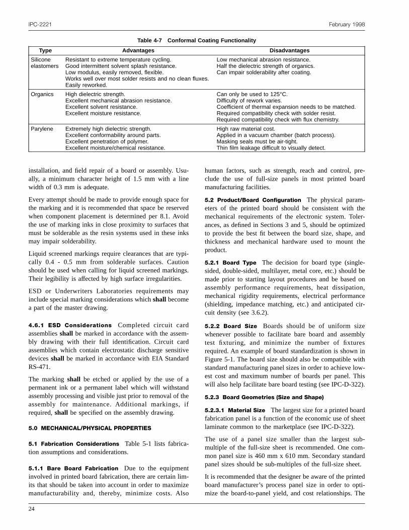
IPC-2221 February 1998
Table 4-7 Conformal Coating Functionality
Type Advantages Disadvantages
Siliconeelastomers
Resistant to extreme temperature cycling.Good intermittent solvent splash resistance.Low modulus, easily removed, flexible.Works well over most solder resists and no clean fluxes.Easily reworked.
Low mechanical abrasion resistance.Half the dielectric strength of organics.Can impair solderability after coating.
Organics High dielectric strength.Excellent mechanical abrasion resistance.Excellent solvent resistance.Excellent moisture resistance.
Can only be used to 125°C.Difficulty of rework varies.Coefficient of thermal expansion needs to be matched.Required compatibility check with solder resist.Required compatibility check with flux chemistry.
Parylene Extremely high dielectric strength.Excellent conformability around parts.Excellent penetration of polymer.Excellent moisture/chemical resistance.
High raw material cost.Applied in a vacuum chamber (batch process).Masking seals must be air-tight.Thin film leakage difficult to visually detect.
ue
forveoidatin
ypongs
ay
m-
itivrd
andtheif
-izeo
re-d
er-edndhe
beonn,eir-
bly
inthw-is).
et
b--rdt.
edti-he
installation, and field repair of a board or assembly. Usally, a minimum character height of 1.5 mm with a linwidth of 0.3 mm is adequate.
Every attempt should be made to provide enough spacethe marking and it is recommended that space be resewhen component placement is determined per 8.1. Avthe use of marking inks in close proximity to surfaces thmust be solderable as the resin systems used in thesemay impair solderability.
Liquid screened markings require clearances that are tcally 0.4 - 0.5 mm from solderable surfaces. Cautishould be used when calling for liquid screened markinTheir legibility is affected by high surface irregularities.
ESD or Underwriters Laboratories requirements minclude special marking considerations whichshall becomea part of the master drawing.
4.6.1 ESD Considerations Completed circuit cardassembliesshall be marked in accordance with the assebly drawing with their full identification. Circuit cardassemblies which contain electrostatic discharge sensdevicesshall be marked in accordance with EIA StandaRS-471.
The markingshall be etched or applied by the use ofpermanent ink or a permanent label which will withstaassembly processing and visible just prior to removal ofassembly for maintenance. Additional markings,required,shall be specified on the assembly drawing.
5.0 MECHANICAL/PHYSICAL PROPERTIES
5.1 Fabrication Considerations Table 5-1 lists fabrica-tion assumptions and considerations.
5.1.1 Bare Board Fabrication Due to the equipmentinvolved in printed board fabrication, there are certain limits that should be taken into account in order to maximmanufacturability and, thereby, minimize costs. Als
24
-
rd
ks
i-
.
e
human factors, such as strength, reach and control, pclude the use of full-size panels in most printed boarmanufacturing facilities.
5.2 Product/Board Configuration The physical param-eters of the printed board should be consistent with thmechanical requirements of the electronic system. Toleances, as defined in Sections 3 and 5, should be optimizto provide the best fit between the board size, shape, athickness and mechanical hardware used to mount tproduct.
5.2.1 Board Type The decision for board type (single-sided, double-sided, multilayer, metal core, etc.) shouldmade prior to starting layout procedures and be basedassembly performance requirements, heat dissipatiomechanical rigidity requirements, electrical performanc(shielding, impedance matching, etc.) and anticipated ccuit density (see 3.6.2).
5.2.2 Board Size Boards should be of uniform sizewhenever possible to facilitate bare board and assemtest fixturing, and minimize the number of fixturesrequired. An example of board standardization is shownFigure 5-1. The board size should also be compatible wistandard manufacturing panel sizes in order to achieve loest cost and maximum number of boards per panel. Thwill also help facilitate bare board testing (see IPC-D-322
5.2.3 Board Geometries (Size and Shape)
5.2.3.1 Material Size The largest size for a printed boardfabrication panel is a function of the economic use of shelaminate common to the marketplace (see IPC-D-322).
The use of a panel size smaller than the largest sumultiple of the full-size sheet is recommended. One common panel size is 460 mm x 610 mm. Secondary standapanel sizes should be sub-multiples of the full-size shee
It is recommended that the designer be aware of the printboard manufacturer’s process panel size in order to opmize the board-to-panel yield, and cost relationships. T

February 1998 IPC-2221
Table 5-1 Fabrication Considerations
Fabrication Design AssumptionsBenefits( ★), Drawbacks( ⇓), Impacts of Not Following Assumptions( ⊗), OtherComments( ✇)
Hole/Land Ratio:Land size at least 0.6 mm greater than thehole size
★Provides sufficient land area to prevent breakout, i.e., hole intersecting edge ofland (insufficient annular ring)
⇓ Large lands may interfere with minimum spacing
Teardrop at Connection of Run withLand
★Provides additional area to prevent breakout.★May improve reliability by preventing cracking at land/run boundary in vibration orthermal cycling.
⇓ May interfere with minimum space requirements
Board Thickness:0.8 mm to 2.4 mm typical (over copper)
⊗Thinner boards tend to warp & require extra handling with through-hole technologycomponents. Thicker boards have lower yield because of layer to layer registration.Some components may not have long enough leads for thicker boards.
Board Thickness to Plated HoleDiameter: Ratios ≤ 5:1 are preferred
★Smaller ratios result in more uniform plating in hole, easier cleaning of holes andless drill wander.
★Larger holes are less susceptible to barrel cracking.
Symmetry across Board Thickness: tophalf should be a mirror image of bottomhalf to achieve a balanced construction
⊗Asymmetrical boards tend to warp.✇The location of ground/power planes, the orientation of signal runs and thedirection of the fabric weave affect board symmetry.
Board Size ★Smaller boards warp less and have better layer to layer registration.⇓ Foil lamination or floating layer lay-ups should be considered for large panels withsmall features
✇Panel utilization determines cost.
Conductor Spacing:≤ 0.1 mm
⊗Etchant fluid does not circulate efficiently in narrower spaces resulting in incompletemetal removal.
Circuit Feature (Conductor Width):≤ 0.1 mm
⊗Smaller features are more susceptible to breakage and damage during etching.
ivrocuc
toos-tryib
thear
oree
ibo
cedndicalingialstheeetteduldanuc-
thenceceThe
theal.n inromure
theheard
use of the larger panel sizes is typically the most effectfrom a labor cost per unit area of end-product board pcessed. However, the use of large panels may pose diffities in achieving fine lines and feature positional accuradue to an increase in base material movement.
5.2.4 Bow and Twist Proper board design, with respecto balanced circuitry construction distribution and compnent placement, is important to minimize the degree of band twist of the printed board. Additionally, the crossectional layout, which includes core thicknesses, dielecthicknesses, inner layer planes, and individual copper lathicknesses, should be kept as symmetrical as possabout the center of the board.
Unless otherwise specified on the master drawing,maximum bow and twistshall be 0.75% for boards that ussurface mount components and 1.5% for all other botechnologies. Panels that contain multiple printed boardsbe assembled on the panel and later separatedshall alsomeet these bow and twist requirements.
If symmetrical construction and tighter tolerances are nsufficient to meet critical assembly or performance requiments, stiffeners or other support hardware may be necsary.
Values are measured per IPC-TM-650, Method 2.4.22.
5.2.5 Structural Strength The wide variety of materialsand resins available places a serious analytical responsity on the designer when structural properties are imp
e-l-y
-w
icerle
e
dto
t-s-
il-r-
tant. The structural properties of laminates are influenby environmental conditions that vary with the lay-up acomposition of the base materials. Physical and electrproperties vary widely over temperature and loadranges. The ultimate properties of printed board materare of marginal use to the designer trying to employprinted board as a structural member. The concern to melectrical performance requirements, which are impacby deformation and elongation of the printed board, shoconsider lower values of ultimate material strength ththose listed in the technical literature for determining strtural needs.
5.2.6 Composite (Constraining-core) Boards Whenstructural, thermal, or electrical requirements dictateuse of a constraining-core board, the physical performapropertiesshall be evaluated using similar conformanspecimen to those designed for standard rigid boards.coupons for the constraining-core boardshall include thecore material.
Whether for thermal or constraining characteristics,board configuration may be symmetrical or asymmetricThere are some advantages in an asymmetrical desigthat the electrical properties or functions are separated fthe mechanical or heat dissipation functions (see Fig5-2).
The drawback of the asymmetrical design is that due todifferences of the coefficient of thermal expansion of tprinted board and the core material, the completed bo
25

IPC-2221 February 1998
IPC-2221-5-1
Figure 5-1 Example of printed board size standardization, mm
350
▼
▼
▼
▼▼
▼
▼
▼▼ ▼
▼ ▼
▼ ▼
▼ ▼
A1
4
3
2
1
A
B
C
D
240
180
120
60
80
170
260
Extractor Hole Size 3 ± 0.10 Dimensions in mm.
Board No.
Printed Board Size 0.4
A1 60 x 80
A2 60 x 170
A3 60 x 260
A4 60 x 350
B1 120 x 80
B2 120 x 170
B3 120 x 260
B4 120 350
C1 180 x 80
C2 180 x 170
C3 180 x 260
C4 180 x 350
D1 240 x 80
D2 240 x 170
D3 240 x 260
D4 240 x 350
[Not recommended for Best Panel Utilization]
26

oompThiena
tri3Altinconkeneblpeofi
gethcl
inin.thllyarrmrdthe
orin
setionol-hat
tatardthem-rddi-of
ecte
ec-ies.ra-r-he
February 1998 IPC-2221
may distort during assembly soldering/reflow operationswhile in system use due to temperature change. Some cpensation can be achieved by having an additional copplane added to the back of the interconnection product.extra copper plane increases the expansion coefficslightly, but a positive effect is that it enhances thermconductivity.
A more desirable construction may be that of the symmecal cored board (see Figure 5-3A and 5-3B). Figure 5-shows the two restraining cores laminated into the mulayer board where they serve as part of the electrical fution, in this case, power and ground. The center core cstruction as shown in Figure 5-3B has a single thicrestraining core which usually has only the thermal plaand restraining function. To achieve restraint in the usarange, the combined thickness of the copper-Invar-copin the multilayer board should be approximately 25%the board thickness. The two-restraining-core boardmore often used because the core layers may be imaetched and connected to the plated through hole;thicker center core must be machined. Better thermal cysurvival is exhibited by the two-restraining-core board.
A special constraining-core board may be made by bonda multilayer printed board to each side of a thick containg metal core after the boards have been completedmore complex variation may also be fabricated whereinconstraining metal core is laminated between two partiacompleted multilayer printed boards. The composite bois then sequentially drilled, plated and etched to foplated-through hole connections between the two boaCoupons should be provided to test the integrity ofcomposite structure.
Metal core boards add significantly to the thermal massthe assembly. This may force the preheating and solde
IPC-2221-5-2
Figure 5-2 Typical asymmetrical constraining-coreconfiguration
Prepreg
Prepreg
Prepreg
Prepreg
Signal (Lands)
Power
Ground
Signal
4-Layer Board
Constraining Core
Solder Resist
Signal
Signal (Lands)
▼▼
r-
eretl
-
---r
er
sd,ee
g-Ae
d
s.
fg
process to be operated at abnormally high limits. Thedesigns should be thoroughly evaluated under producconditions prior to release. Laminate ruptures and discoration and grainy or textured solder are typical effects thave been observed.
5.2.7 Vibration Design The design of printed boards thawill be subjected to vibration while in service requires thspecial consideration be given to the board prior to bolayout. The effect on the board assembly caused byvibration can seriously reduce the reliability of the assebly. The interrelationship between the unit, printed boaassemblies, their mounting and the environmental contions make necessary the need for a vibration analysisthe complete system very early in the design. The efffrom vibration on any item within a unit can make thvibration analysis very complex.
Vibration analysis should be done on each piece of eltronic hardware which contains printed board assemblThe complexity of the analysis should depend on the vibtion level to which the hardware will be subjected in sevice. The design of the printed boards will depend on t
IPC-2221-5-3a
Figure 5-3A Multilayer Metal Core Board with TwoSymmetrical Copper-Invar-Copper Constraining Cores(when the Copper-Invar-Copper planes are connected tothe plated-through hole, use thermal relief per Figure 9-4)
IPC-2221-5-3b
Figure 5-3B Symmetrical Constraining Core Board with aCopper-Invar-Copper Center Core
27

no
osx
te
e-
tyn
heil
po
reth
re
fo
o
ul
.
ndotioa
icaanaIhar
2),ds
ohe
entm-atrd.at
tont,eir
rd,ialand
nted
edina-
m-erlyint.
ect.2).
ntsandht-i-enceedbeact
osebeed,theng.ofing
be
IPC-2221 February 1998
level of vibration transmitted to the board. Particular attetion should be given to printed boards subjected to randvibration.
The following criteria should be used as guidelines fdetermining if the level of vibration to which the boardwill be subjected is a level which would require complevibration analysis of the board:
• The random spectral density is at, or above, 0.1G2/Hz inthe frequency range of 80 to 500 hertz or an unsupporboard distance of greater than 76.2 mm.
• A sinusoidal vibration level at, or above, 3 Gs at a frquency of 80 to 500 Hz.
• The board assembly will be subjected to ReliabiliDevelopment Growth Testing (RDGT) at a spectral desity at, or above, 0.07 G2/Hz for more than 100 hours inconjunction with temperature cycling.
The following guidelines should be observed during tdesign of printed boards to eliminate vibration induced faures of the printed board assemblies:
• The board deflection, from vibration, should be kebelow 0.08 mm per mm of board length (or width) tavoid lead failure on multiple lead devices.
• Positive support of all components with a weight of mothan 5.0 gm per lead should be considered whenboard will be subjected to vibration (see 5.3.2).
• Board stiffeners and/or metal cores should be consideto reduce the board deflection.
• Cushioned mounting of relays should be consideredtheir usage in high level vibration environments.
• Vibration isolators should be considered for mountingunits whenever practical.
• The mounting height of freestanding components shobe kept to a minimum.
• Non-axial leaded components should be side-mounted
Because of the interrelationship of the many componethat makeup a system, the use of the above guidelinesnot ensure the success of a unit subjected to a vibratest. A vibration test of a unit is the only way to ensure tha unit will be reliable in service.
5.3 Assembly Requirements
5.3.1 Mechanical Hardware Attachment The printedboardshall be designed in such a manner that mechanhardware can be easily attached, either prior to the mcomponent mounting effort, or subsequently. Sufficiephysical and electrical clearance should be provided formechanical hardware that requires electrical isolation.general, mounting hardware should protrude no more t6.4 mm below the board surface to allow sufficient cleaances for assembly equipment and solder nozzles.
28
-m
r
d
-
-
t
e
d
r
f
d
tsesnt
lintllnn-
5.3.2 Part Support All parts weighing 5.0 gm, or more,per leadshall be supported by specified means (see 8.1.1which will help ensure that their soldered joints and leaare not relied upon for mechanical strength.
The reliability of printed boards that will be subject tshock and vibration in service require consideration of tfollowing criteria:
• The worst-case levels of shock and vibration environmfor the entire structure in which the printed board assebly resides, and the ultimate level of this environment this actually transmitted to the components on the boa(Particular attention should be given to equipment thwill be subjected to random vibration.)
• The method of mounting the board in the equipmentreduce the effects of the shock and vibration environmespecifically the number of board mounting supports, thinterval, and their complexity.
• The attention given to the mechanical design of the boaspecifically its size, shape, type of material, materthickness, and the degree of resistance to bowingflexing that the design provides.
• The shape, mass and location of the components mouon the board.
• The component lead wire stress relief design as providby its package, lead spacing, lead bending, or a combtion of these, plus the addition of restraining devices.
• The attention paid to workmanship during board assebly, so as to ensure that component leads are propbent, not nicked, and that the components are installeda manner that tends to minimize component movemen
• Conformal coating may also be used to reduce the effof shock and vibration on the board assembly (see 4.5
Where circuit design permits, the selection of componeto be mounted on boards subjected to severe shockvibration should favor the use of components that are ligweight, have low profiles and inherent strain-relief provsions. Where discrete components must be used, prefershould be given to surface mount and/or axially-leadtypes that present a relatively low profile that canmounted and easily clamped or bonded in intimate contwith the board surface.
The use of irregularly-shaped components, especially thhaving a large mass and a high center of gravity, shouldavoided where practical. If their use cannot be avoidthey should be located toward the outer perimeter ofboard, or where hardware or mounting reduces flexiDepending on the severity of this problem, the usemechanical clamping, adhesive bonding, or embeddmay be required.
5.3.3 Assembly and Test Consideration, similar to thatmentioned above for printed board fabrication, must
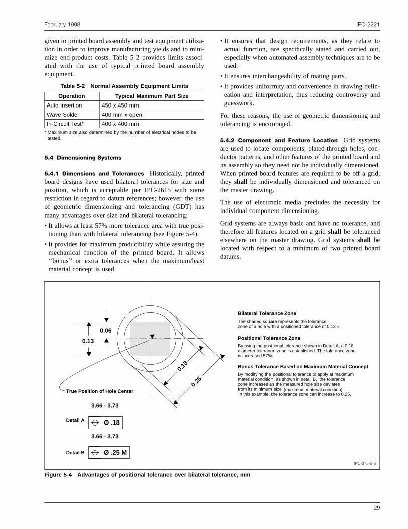
izi-cbl
a
ua
s.
ess
tot,be
-nd
nd
on-ndd.id,n
for
and
d
February 1998 IPC-2221
given to printed board assembly and test equipment utiltion in order to improve manufacturing yields and to minmize end-product costs. Table 5-2 provides limits assoated with the use of typical printed board assemequipment.
5.4 Dimensioning Systems
5.4.1 Dimensions and Tolerances Historically, printedboard designs have used bilateral tolerances for sizeposition, which is acceptable per IPC-2615 with somrestriction in regard to datum references; however, theof geometric dimensioning and tolerancing (GDT) hmany advantages over size and bilateral tolerancing:
• It allows at least 57% more tolerance area with true potioning than with bilateral tolerancing (see Figure 5-4)
• It provides for maximum producibility while assuring thmechanical function of the printed board. It allow‘‘bonus’’ or extra tolerances when the maximum/leamaterial concept is used.
Table 5-2 Normal Assembly Equipment Limits
Operation Typical Maximum Part Size
Auto Insertion 450 x 450 mm
Wave Solder 400 mm x open
In-Circuit Test* 400 x 400 mm* Maximum size also determined by the number of electrical nodes to betested.
a-
i-y
ndeses
i-
t
• It ensures that design requirements, as they relateactual function, are specifically stated and carried ouespecially when automated assembly techniques are toused.
• It ensures interchangeability of mating parts.
• It provides uniformity and convenience in drawing delineation and interpretation, thus reducing controversy aguesswork.
For these reasons, the use of geometric dimensioning atolerancing is encouraged.
5.4.2 Component and Feature Location Grid systemsare used to locate components, plated-through holes, cductor patterns, and other features of the printed board aits assembly so they need not be individually dimensioneWhen printed board features are required to be off a grthey shall be individually dimensioned and toleranced othe master drawing.
The use of electronic media precludes the necessityindividual component dimensioning.
Grid systems are always basic and have no tolerance,therefore all features located on a gridshall be tolerancedelsewhere on the master drawing. Grid systemsshall belocated with respect to a minimum of two printed boardatums.
IPC-275-5-5
Figure 5-4 Advantages of positional tolerance over bilateral tolerance, mm
▼
▼
▼
▼0.2
5
0.18
True Position of Hole Center
0.06
0.13
▼
▼ ▼
▼ ▼
Bilateral Tolerance Zone
The shaded square represents the tolerance zone of a hole with a positioned tolerance of 0.13 ± .
Positional Tolerance Zone
By using the positional tolerance shown in Detail A, a 0.18 diameter tolerance zone is established. The tolerance zone is increased 57%.
Bonus Tolerance Based on Maximum Material Concept
By modifying the positional tolerance to apply at maximum material condition, as shown in detail B, the tolerance zone increases as the measured hole size deviates from its minimum size (maximum material condition).In this example, the tolerance zone can increase to 0.25.
Ø .18
3.66 - 3.73
Detail A
Detail B
3.66 - 3.73
Ø .25 M
29

d
th
ru
ettela
em
inte
ry-te
arthhn
1edoate
icob
s
it
hest
estea-
srese
tumaa-orblyInbe-ceol-
onndcenrisAseiseol-
ec-
n
ndheriali-rd
IPC-2221 February 1998
The selected grid increment or the use of electronic meshall be specified on the master drawing. The componeterminal location for through-hole components or the component center location for surface mount componentsestablished by either the selected grid increment orelectronic media.
Typical grid increments are multiples of 0.5 mm fothrough-hole components, and 0.05 mm for surface mocomponents.
5.4.3 Datum Features Datum features indicate the ori-gin of a dimensional relationship between a toleranced fture and a designated feature or features on the prinboard. Datum features are chosen to position the prinboard in relation to a set of three mutually perpendicuplanes (see Figure 5-5, A-E).
There are some cases where a single datum referencsufficient, for example a printed board profile or a datuhole position.
Typically, printed board drawings are oriented with the prmary (component) side or the designated Layer 1 faciup. This orientation establishes the backside of the prinboard as the first (primary (‘‘A’’)) of the three requireddatum planes.
The other two datum planes (secondary (‘‘B’’) and tertia(‘‘C’’)) are typically established at minimum material conditions using holes and/or etched features on the prinboard.
The choice of features to be used for datums dependswhat design elements are intended to be controlled. Boedge or feature edge datums should not be used primabecause their use may not represent the function ofprinted board. They also pose producibility problems to tfabricator. Coordinate zero should be located at the secoary datum feature. Datum featuresshall be specified on themaster drawing by means of datum symbols per IPC-26The use of implied datums is not allowed. Datum featurshall be functional features of the printed board, anshould relate to mating parts such as mounting holes, cnectors, or component leads or terminations. All datum fetures should be located on grid or establish the grid cririon, and theyshall be located within the printed boardprofile.
To maximize the total available tolerance, a good practis to separately locate and tolerance as patterns thprinted board features that are produced in separate facation operations. Applicable patterns are as follows:
A. Plated Through-Hole PatternsThe plated through-hole pattern (see Figure 5-5A) is generally the firdrilling operation and is the first operation that definethe printed board. It is dimensioned as a basic grid w
30
iant-ise
nt
a-eddr
is
-gd
d
onrdilyeed-
5.s
n---
eseri-
tsh
each hole toleranced to a basic grid intersection. Thole location tolerance is specified either in the hole lior by drawing note. A minimum of two holes on thegrid shall be dimensioned and toleranced andshallestablish the primary datum reference frame.
B. Unplated Through Hole PatternsUnplated through-hole patterns, especially tooling and mounting hol(see Figure 5-5B), are generally drilled in a separadrilling operation as one of the last fabrication opertions. Theyshall be explicitly dimensioned and toler-anced, even if they occur on grid. Two of these holeare typically established as secondary datum featubecause of their function, in spite of their place in thfabrication sequence.
C. Conductor PatternsThe conductor pattern does noneed a separate datum reference provided a minimannular ring is specified. Minimum annular ring iscommon way to tolerance the conductor pattern loction with respect to the plated through-hole pattern. Fsome designs, particularly where automated assemis used, this method may allow too much tolerance.these cases, a feature location tolerance mayrequired andshall appear on the master drawing. Alternately, fiducials may be required to locate and toleranthe conductor pattern with respect to the assembly toing holes (see Figure 5-5C).
The fiducial size, shape and quantity may dependthe type of equipment used in the assembly process alead pitch and lead count. Figure 5-6 shows the SurfaMount Equipment Manufacturers Associatio(SMEMA) recommended fiducial design. Anothemethod to locate and tolerance the conductor patternby dimensioning to the centerline of a conductor.critical area is edge board connector contacts; theshould be dimensional as shown in Figure 5-7. Thfigure establishes a second X datum from which thtang edge is established as well as any keying slot. Terances used for edgeboard and keying slotsshall besuch that keying slots do not cut into or damage thcontact finger. Dimensioning to the edge of a condutor is not allowed.
Figure 5-5E shows how Figures 5-5A through 5-5D cabe assembled into one drawing.
D. Printed Board Profile The printed board profile,including cutouts and notches (see Figures 5-5D a5-7), requires a minimum of one datum reference. Tuse of three datum references and maximum matecondition modifiers, as shown in Figure 5-5D, maxmizes allowable tolerances and allows the use of hatool gauging, which is particularly useful in high vol-ume production situations.
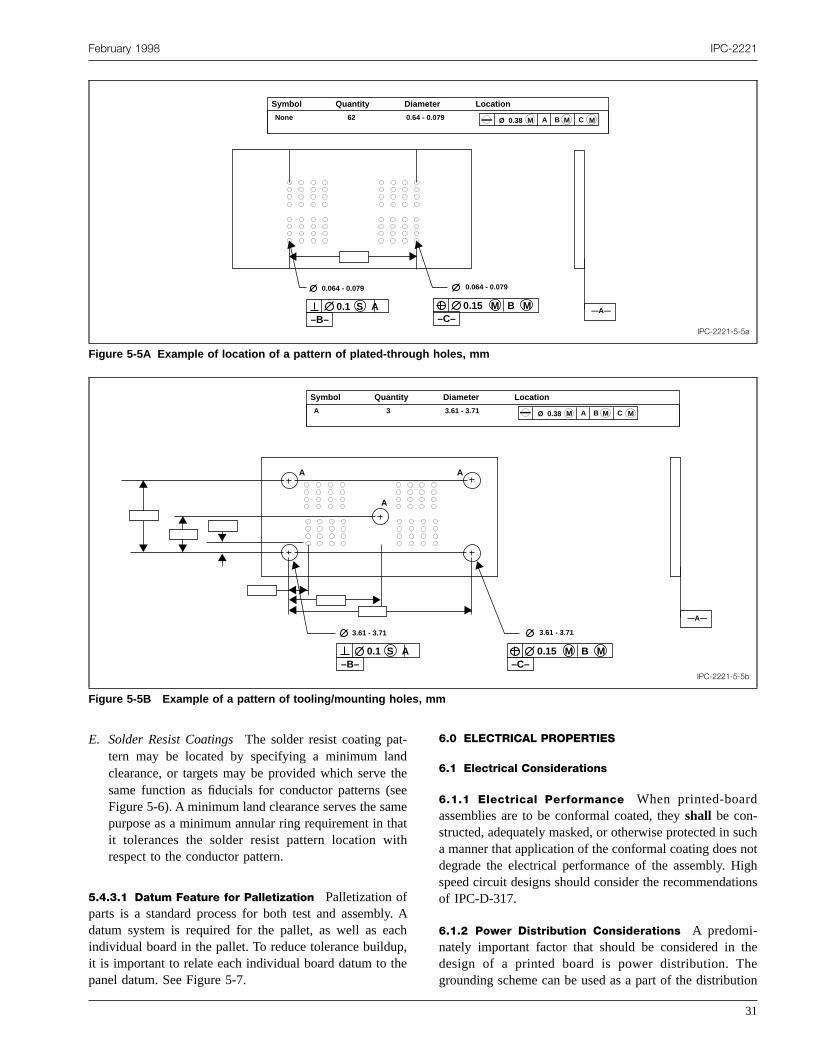
February 1998 IPC-2221
IPC-2221-5-5a
Figure 5-5A Example of location of a pattern of plated-through holes, mm
▼ ▼
—A—
MAMØ 0.38 B M C
Symbol Quantity Diameter Location
62 0.64 - 0.079None
▼ ▼
0.064 - 0.079 0.064 - 0.079
0.1 S A–B–
0.15 M B M–C–
IPC-2221-5-5b
Figure 5-5B Example of a pattern of tooling/mounting holes, mm
▼
▼
▼
▼▼▼
▼ ▼
A
AA
▼ ▼
—A—
MAMØ 0.38 B M C
Symbol Quantity Diameter Location
3 3.61 - 3.71A
▼ ▼
▼▼
3.61 - 3.71 3.61 - 3.71
0.1 S A–B–
0.15 M B M–C–
t-ndthsemhaith
ly.acphe
uchnotighions
heetion
E. Solder Resist CoatingsThe solder resist coating patern may be located by specifying a minimum laclearance, or targets may be provided which servesame function as fiducials for conductor patterns (Figure 5-6). A minimum land clearance serves the sapurpose as a minimum annular ring requirement in tit tolerances the solder resist pattern location wrespect to the conductor pattern.
5.4.3.1 Datum Feature for Palletization Palletization ofparts is a standard process for both test and assembdatum system is required for the pallet, as well as eindividual board in the pallet. To reduce tolerance builduit is important to relate each individual board datum to tpanel datum. See Figure 5-7.
eeet
Ah,
6.0 ELECTRICAL PROPERTIES
6.1 Electrical Considerations
6.1.1 Electrical Performance When printed-boardassemblies are to be conformal coated, theyshall be con-structed, adequately masked, or otherwise protected in sa manner that application of the conformal coating doesdegrade the electrical performance of the assembly. Hspeed circuit designs should consider the recommendatof IPC-D-317.
6.1.2 Power Distribution Considerations A predomi-nately important factor that should be considered in tdesign of a printed board is power distribution. Thgrounding scheme can be used as a part of the distribu
31
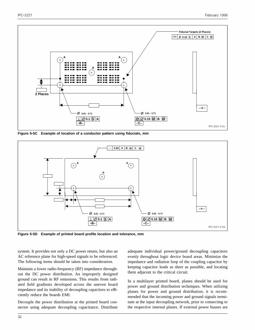
IPC-2221 February 1998
IPC-2221-5-5c
Figure 5-5C Example of location of a conductor pattern using fiducials, mm
2 Places
▼
▼
▼ ▼
A
AA
▼ ▼
—A—
Fiducial Targets (2 Places)
MASØ 0.15 B M C
▼
3.61 - 3.71 3.61 - 3.71
0.1 S A–B–
0.15 M B M–C–
IPC-2221-5-5d
Figure 5-5D Example of printed board profile location and tolerance, mm
▼
▼
▼ ▼
A
AA
▼ ▼
—A—
▼ ▼▼▼
▼
M0.50 A B M C
▼
▼
3.61 - 3.71 3.61 - 3.71
0.1 S A–B–
0.15 M B M–C–
ance
h-ddiaffi-
nu
rsebyting
org-i-toare
system. It provides not only a DC power return, but alsoAC reference plane for high-speed signals to be referenThe following items should be taken into consideration.
Maintain a lower radio-frequency (RF) impedance througout the DC power distribution. An improperly designeground can result in RF emissions. This results from raated field gradients developed across the uneven boimpedance and its inability of decoupling capacitors to eciently reduce the boards EMI.
Decouple the power distribution at the printed board conector using adequate decoupling capacitance. Distrib
32
d.
-rd
-te
adequate individual power/ground decoupling capacitoevenly throughout logic device board areas. Minimize thimpedance and radiation loop of the coupling capacitorkeeping capacitor leads as short as possible, and locathem adjacent to the critical circuit.
In a multilayer printed board, planes should be used fpower and ground distribution techniques. When utilizinplanes for power and ground distribution, it is recommended that the incoming power and ground signals termnate at the input decoupling network, prior to connectingthe respective internal planes. If external power busses

February 1998 IPC-2221
IPC-2221-5-5e
Figure 5-5E Example of a printed board drawing utilizing geometric dimensioning and tolerancing, mm
2 Places
▼
▼
▼ ▼
A
AA
▼ ▼
—A—
Fiducial Targets (2 Places)
MAS B M C
▼
M0.5 A B M C
Symbol Quantity Diameter Location
64 3.64 - 3.79None
MAMØ 0.38 B M C
MAMØ 0.15 B M C
3 3.61 - 3.71A
Ø 0.15
▼
▼▼▼▼
▼▼
3.61 - 3.71 3.61 - 3.71
0.1 S A–B–
0.15 M B M–C–
ywdahet
cetalk.
bu-nd
her
ndoner,pos-oid-undn-ade
sedatedits
ard
required, commercially available bussing schemes maemployed as defined in section 8.2.13. When using poconductors, as shown in Figure 6-1, power traces shoulrun as close as possible to ground traces. Both powerground tracesshall be maintained as wide as possible. Tpower and ground planes virtually become one planhigh frequencies, and should, therefore, be kept nexeach other.
IPC-2221-5-6
Figure 5-6 Fiducial clearance requirements
R
2R
Clearance
R
3R
Clearance
Minimum Preferred
▼
▼ ▼ ▼ ▼
▼ ▼ ▼
beerbendeatto
Figure 6-1A shows a poor layout, giving high inductanand few adjacent signal return paths; this leads to cross
Figure 6-1B is a better layout and reduces power distrition, logic-return impedances, conductor crosstalk aboard radiation.
The best layout is shown in Figure 6-1C, which has furtEMI problem reductions.
In digital power distribution schemes, the grounding apower should be designed first, not last, as is typically dwith some analog circuits. All interfacing, including poweshould be routed to a single reference edge, or area. Oping end interconnections are to be avoided. When unavable, care should be taken to route the power and groaway from active circuits (see Figure 6-2). At the interconection reference edge, all ground structures are to be mas heavy as possible.
The shortest possible conductor length should be ubetween devices. The printed board should be separinto areas for high, medium, and low frequency circu(see Figure 6-3).
6.1.3 Circuit Type Considerations The following guide-lines should be considered when designing printed boassemblies:
33
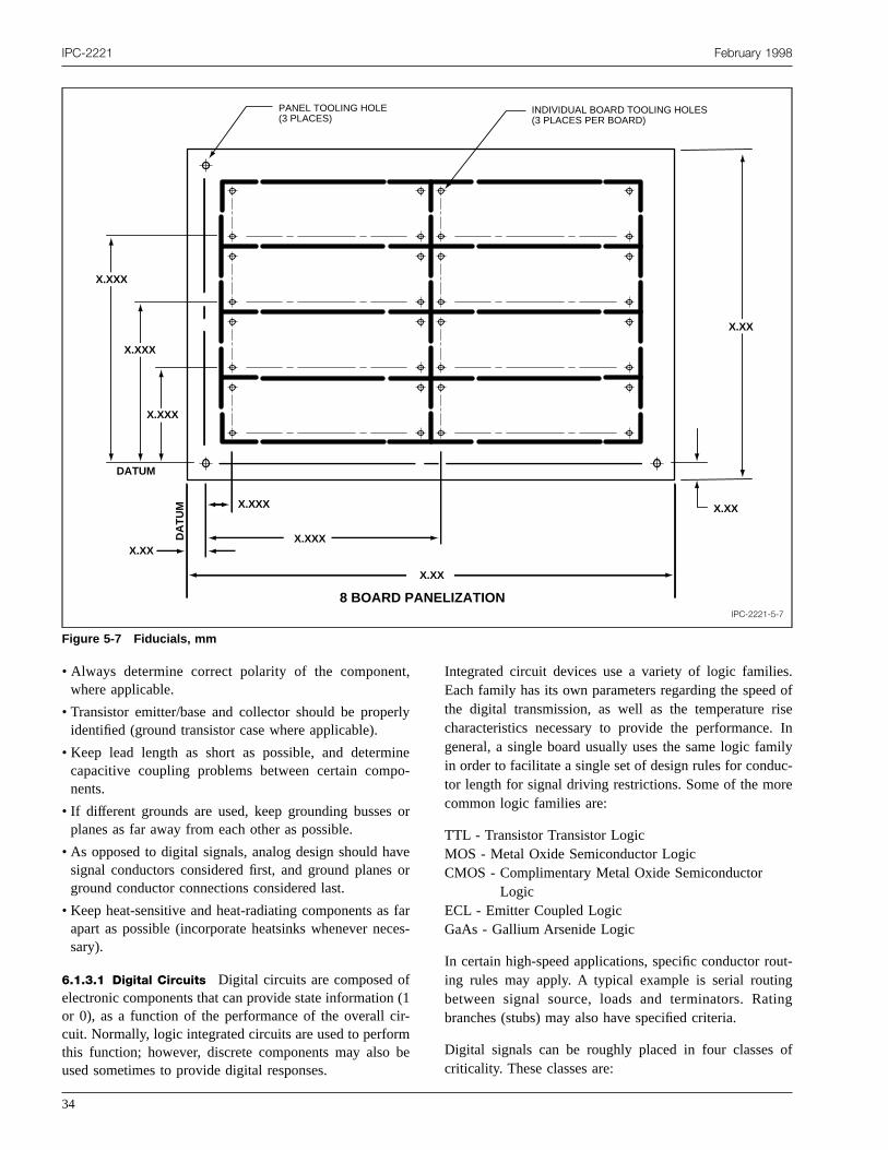
IPC-2221 February 1998
IPC-2221-5-7
Figure 5-7 Fiducials, mm
X.XX
X.XX
X.XXX
X.XXX
X.XXX
X.XX
X.XXX
DATUM
DA
TU
M
X.XXX
X.XX
8 BOARD PANELIZATION
PANEL TOOLING HOLE (3 PLACES)
INDIVIDUAL BOARD TOOLING HOLES (3 PLACES PER BOARD)
t,
rly
ino-
o
aveo
face
f(1ir-mbe
.ofseInilyc-e
t-
ng
f
• Always determine correct polarity of the componenwhere applicable.
• Transistor emitter/base and collector should be propeidentified (ground transistor case where applicable).
• Keep lead length as short as possible, and determcapacitive coupling problems between certain compnents.
• If different grounds are used, keep grounding bussesplanes as far away from each other as possible.
• As opposed to digital signals, analog design should hsignal conductors considered first, and ground planesground conductor connections considered last.
• Keep heat-sensitive and heat-radiating components asapart as possible (incorporate heatsinks whenever nesary).
6.1.3.1 Digital Circuits Digital circuits are composed oelectronic components that can provide state informationor 0), as a function of the performance of the overall ccuit. Normally, logic integrated circuits are used to perforthis function; however, discrete components may alsoused sometimes to provide digital responses.
34
e
r
r
rs-
Integrated circuit devices use a variety of logic familiesEach family has its own parameters regarding the speedthe digital transmission, as well as the temperature richaracteristics necessary to provide the performance.general, a single board usually uses the same logic famin order to facilitate a single set of design rules for condutor length for signal driving restrictions. Some of the morcommon logic families are:
TTL - Transistor Transistor LogicMOS - Metal Oxide Semiconductor LogicCMOS - Complimentary Metal Oxide Semiconductor
LogicECL - Emitter Coupled LogicGaAs - Gallium Arsenide Logic
In certain high-speed applications, specific conductor rouing rules may apply. A typical example is serial routingbetween signal source, loads and terminators. Ratibranches (stubs) may also have specified criteria.
Digital signals can be roughly placed in four classes ocriticality. These classes are:

February 1998 IPC-2221
IPC-275-4-48
Figure 5-8 Example of connector key slot location and tolerance, mm▼
▼ ▼
T
Tolerance applied to this feature must correlate with the tolerance applied to the conductor pattern location
▼▼–D–
0.251.14 - 1.40
▼
▼L A D S
r
s
gy
aeeh
e
-r-t
-o
ingenr-n-Inising
an-des,ys,ices
rdt-blethrted
asm-xi-he
1. Non-Critical Signals- are not sensitive to couplingbetween them. Examples are between the lines ofdata bus or between the lines of an address bus whethey are sampled long after they are settled.
2. Semi-Critical Signals- are those where coupling mustbe kept low enough to avoid false triggering, such areset lines and level triggering strobe lines.
3. Critical Signals- have waveforms that must be mono-tonic through the voltage thresholds of the receivindevice. These are normally clocking signals and anglitch while the wave form is in transition may causea double clocking of the circuit. A non-critical signalhas a waveform that need not be monotonous and meven make multiple transitions between the voltagthresholds before it settles. Obviously it must settlbefore the receiving device acts upon the data, e.g., tdata input to a flip-flop may be a non-critical but theclock signal is most probably a critical signal. Asyn-chronous signals, although they may (or may not) bnon-critical signals, should not be mixed with criticalsignals since there is a real possibility of the asynchronous signals inducing noise on the critical signals duing the clock transitions. Clock signals that do nohave a common master frequency should also not brouted together for similar reasons.
4. Super-Critical Signals- are those in applications suchas clocks or strobes for A/D and D/A converters, signals in Phase Locked Loops, etc. In these types
ae
y
e
e
f
applications phase lock jitters and crosstalk, causerrors, noise and timing jitters, will show up in thapplication’s output performance. It is only a questioof the amount of disturbance within the required peformance specification. This class of signal is essetially the same as an analog coupling situation.other words, it is completely linear (the total noisethe sum of the individual noise elements; no averagof canceling out can be assumed).
6.1.3.2 Analog Circuits Analog circuits are usuallymade from integrated circuits and discrete devices.. Stdard discrete components (resistors, capacitors, diotransistors, etc.), as well as power transformers, relacoils and chokes, are usually the types of discrete devused for analog circuits.
6.2 Conductive Material Requirements The minimumwidth and thickness of conductors on the finished boashall be determined primarily on the basis of the currencarrying capacity required, and the maximum permissiconductor temperature rise. The minimum conductor widand thicknessshall be in accordance with Figure 6-4 foconductors on external and internal layers of the prinboard.
The conductor’s permissible temperature rise is definedthe difference between the maximum safe operating teperature of the printed board laminate material and mamum temperature of the thermal environment to which t
35
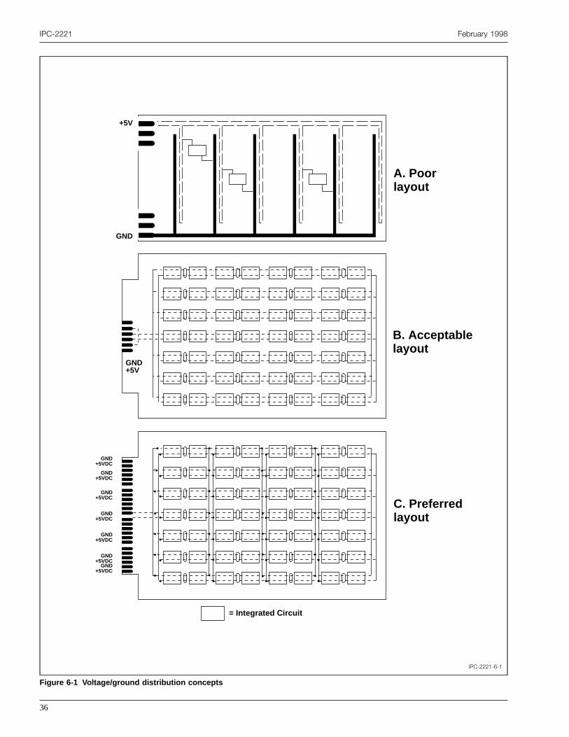
IPC-2221 February 1998
IPC-2221-6-1
Figure 6-1 Voltage/ground distribution concepts
C. Preferred layout
GND +5V
GND +5VDC
GND +5VDC
GND +5VDC
GND +5VDC
GND +5VDC
GND +5VDC
GND +5VDC
= Integrated Circuit
+5V
GND
B. Acceptable layout
A. Poor layout
• •
•
•
•
•
•
•
•
•
•
•
•
•
•
•
•
•
•
•
•
•
•
•
•
•
••
•
•
•
•
•
• •
•
•
•
•
•
•
•
•
•
•
•
•
•
•
•
•
•
•
•
36

February 1998 IPC-2221
IPC-275-3-10
Figure 6-2 Single reference edge routing
Recommended
Ground
Power
▼
▼
Not Recommended
Power
▼Ground
▼
ledtheardem-e isoledoardred.n aem-partsd/orthetheo be
perviasdesctorperbuteadthefor
IPC-275-3-11
Figure 6-3 Circuit distribution
Low Frequency
Circuits
Medium Frequency
Circuits
High Frequency
Circuits
essForary
printed board will be subjected. For convection-cooprinted board assemblies, the thermal environment ismaximum ambient temperature where the printed bowill be used. For conduction-cooled printed board assblies in a convection environment, the temperature riscaused by the dissipated power of the conduction-coparts and the temperature rise through the printed band/or heatsink to the cold plate should also be consideFor conduction-cooled printed board assemblies ivacuum environment, the thermal environment is the tperature rise caused by the dissipated power of theand the temperature rise through the printed board anheatsink to the cold plate. In a vacuum environment,effects of radiation heat transfer between the parts,printed board assembly and the cold plate should alsconsidered.
For internal layers, the conductor thickness is the copfoil thickness of the base laminate unless blind/buriedare used in which case the copper foil thickness inclucopper process plating. For external layers, the conduthickness also includes the thickness of plated copdeposited during the plated-through hole process,should not include the thickness of solder coating, tin-lplating, or secondary platings. It should be noted thatfoil thickness specified by the standard drawing notedthe preferred printed board materials are nominal thicknvalues which can generally vary by as much as ± 10%.external layers, the total copper thickness will also v
37

n
s
IPC-2221 February 1998
IPC-2221-6-4
Figure 6-4 Conductor thickness and width for internal and external layers
Notes:
1. The design chart has been prepared as aaid in estimating temperature rises (aboveambient) vs. current for various cross-sectional areas of etched copper conduc-tors. It is assumed that, for normal design,conditions prevail where the conductor sur-face area is relatively small compared tothe adjacent free panel area. The curves apresented include a nominal 10 percentderating (on a current basis) to allow fornormal variations in etching techniques,copper thickness, conductor width esti-mates, and cross-sectional area.
2. Additional derating of 15 percent (current-wise) is suggested under the following con-ditions:
(a) For panel thickness of 0.8 mm or less
(b) For conductor thickness of 108 µm orthicker.
3. For general use the permissible tempera-ture rise is defined as the differencebetween the ambient temperature and themaximum sustained operating temperatureof the assembly.
4. For single conductor applications the chartmay be used directly for determining con-ductor widths, conductor thickness, cross-sectional area, and current-carrying capac-ity for various temperature rises.
5. For groups of similar parallel conductors, ifclosely spaced, the temperature rise may befound by using an equivalent cross-sectionand an equivalent current. The equivalentcross-section is equal to the sum of thecross-section of the parallel conductors,and the equivalent current is the sum of thecurrents in the conductors.
6. The effect of heating due to attachment ofpower dissipating parts is not included.
7. The conductor thicknesses in the designchart do not include conductor overplatingwith metals other than copper.
38
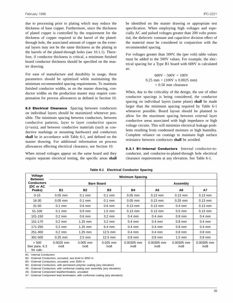
thnehedxtgeda
ethtaom1
rsoseceooths0
th
este-en-ofhe
eslec-d
ertor
-1toerigh-ity.ce
cal.
February 1998 IPC-2221
due to processing prior to plating which may reducethickness of base copper. Furthermore, since the thickof plated copper is controlled by the requirement for tthickness of copper required in the barrel of the platthrough hole, the associated amount of copper on the enal layers may not be the same thickness as the platinthe barrels of the plated-through holes (see 10.1.1). Thfore, if conductor thickness is critical, a minimum finisheboard conductor thickness should be specified on the mter drawing.
For ease of manufacture and durability in usage, thparameters should be optimized while maintainingminimum recommended spacing requirements. To mainfinished conductor widths, as on the master drawing, cductor widths on the production master may require copensation for process allowances as defined in Section
6.3 Electrical Clearance Spacing between conductoon individual layers should be maximized whenever psible. The minimum spacing between conductors, betwconductive patterns, layer to layer conductive spa(z=axis), and between conductive materials (such as cductive markings or mounting hardware) and conductshall be in accordance with Table 6-1, and defined onmaster drawing. For additional information on proceallowances effecting electrical clearance, see Section 1
When mixed voltages appear on the same board andrequire separate electrical testing, the specific areasshall
esse-er-inre-
s-
seeinn--0.
-ensn-rses.
ey
be identified on the master drawing or appropriate tspecification. When employing high voltages and espcially AC and pulsed voltages greater than 200 volts pottial, the dielectric constant and capacitive division effectthe material must be considered in conjunction with trecommended spacing.
For voltages greater than 500V, the (per volt) table valumust be added to the 500V values. For example, the etrical spacing for a Type B1 board with 600V is calculateas:
600V - 500V = 100V0.25 mm + (100V x 0.0025 mm)
= 0.50 mm clearance
When, due to the criticality of the design, the use of othconductor spacings is being considered, the conducspacing on individual layers (same plane)shall be madelarger than the minimum spacing required by Table 6whenever possible. Board layout should be plannedallow for the maximum spacing between external layconductive areas associated with high impedance or hvoltage circuits. This will minimize electrical leakage problems resulting from condensed moisture or high humidComplete reliance on coatings to maintain high surfaresistance between conductorsshall be avoided.
6.3.1 B1-Internal Conductors Internal conductor-to-conductor, and conductor-to-plated-through hole electriclearance requirements at any elevation. See Table 6-1
Table 6-1 Electrical Conductor Spacing
VoltageBetween
Conductors(DC or ACPeaks)
Minimum Spacing
Bare Board Assembly
B1 B2 B3 B4 A5 A6 A7
0-15 0.05 mm 0.1 mm 0.1 mm 0.05 mm 0.13 mm 0.13 mm 0.13 mm
16-30 0.05 mm 0.1 mm 0.1 mm 0.05 mm 0.13 mm 0.25 mm 0.13 mm
31-50 0.1 mm 0.6 mm 0.6 mm 0.13 mm 0.13 mm 0.4 mm 0.13 mm
51-100 0.1 mm 0.6 mm 1.5 mm 0.13 mm 0.13 mm 0.5 mm 0.13 mm
101-150 0.2 mm 0.6 mm 3.2 mm 0.4 mm 0.4 mm 0.8 mm 0.4 mm
151-170 0.2 mm 1.25 mm 3.2 mm 0.4 mm 0.4 mm 0.8 mm 0.4 mm
171-250 0.2 mm 1.25 mm 6.4 mm 0.4 mm 0.4 mm 0.8 mm 0.4 mm
251-300 0.2 mm 1.25 mm 12.5 mm 0.4 mm 0.4 mm 0.8 mm 0.8 mm
301-500 0.25 mm 2.5 mm 12.5 mm 0.8 mm 0.8 mm 1.5 mm 0.8 mm
> 500See para. 6.3
for calc.
0.0025 mm/volt
0.005 mm/volt
0.025 mm/volt
0.00305 mm/volt
0.00305 mm/volt
0.00305 mm/volt
0.00305 mm/volt
B1 - Internal ConductorsB2 - External Conductors, uncoated, sea level to 3050 mB3 - External Conductors, uncoated, over 3050 mB4 - External Conductors, with permanent polymer coating (any elevation)A5 - External Conductors, with conformal coating over assembly (any elevation)A6 - External Component lead/termination, uncoatedA7 - External Component lead termination, with conformal coating (any elevation)
39

dntsouct-of
na
t-rrdallteot
ndnerre
e
ears.
lee
reysere
s,e
ryne
dord
lec-ter-nd
d-nly
re-s-
tlythof-
ricr-
m-
ke-
r-heA).oner)ys-es,
IPC-2221 February 1998
6.3.2 B2-External Conductors, Uncoated, Sea Level to3050 m Electrical clearance requirements for uncoateexternal conductors are significantly greater than for coductors that will be protected from external contaminanwith conformal coating. If the assembled end product is nintended to be conformally coated, the bare board condtor spacingshall require the spacing specified in this caegory for applications from sea level to an elevation3050 m. See Table 6-1.
6.3.3 B3-External Conductors, Uncoated, Over 3050 mExternal conductors on uncoated bare board applicatioover 3050 m require even greater electrical spacings ththose identified in category B2. See Table 6-1.
6.3.4 B4-External Conductors, with Permanent PolymerCoating (Any Elevation) When the final assembled boardwill not be conformally coated, a permanent polymer coaing over the conductors on the bare board will allow foconductor spacings less than that of the uncoated boadefined by category B2 and B3. The assembly electricclearances of lands and leads that are not conformacoated require the electrical clearance requirements stain category A6 (see Table 6-1). This configuration is napplicable for any application requiring protection fromharsh, humid, contaminated environments.
Typical applications are computers, office equipment, acommunication equipment, bare boards operating in cotrolled environments in which the bare boards have a pmanent polymer coating on both sides. After they aassembled and soldered the boards are not conformcoated, leaving the solder joint and soldered land uncoat
Note: All conductors, except for soldering lands, must bcompletely coated in order to ensure the electrical cleance requirements in this category for coated conductor
6.3.5 A5-External Conductors, with Conformal CoatingOver Assembly (Any Elevation) Externalconductors thatare intended to be conformal coated in the final assembconfiguration, for applications at any elevation, will requirthe electrical clearances specified in this category.
Typical applications are military products where the entifinal assembly will be conformal coated. Permanent polmer coatings are not normally used, except for possible uas a solder resist. However, the compatibility of polymcoating and conformal coating must be considered, if usin combination.
6.3.6 A6-External Component Lead/Termination,Uncoated External component leads and terminationthat are not conformal coated, require electrical clearancstated in this category.
Typical applications are as previously stated in categoB4. The B4/A6 combination is most commonly used icommercial, non-harsh environment applications in ord
40
-
t-
sn
slyd
--
ald.
-
d
-e
d
s
r
to obtain the benefit of high conductor density protectewith permanent polymer coating (also solder resist),where the accessibility to components for rework anrepair is not required.
6.3.7 A7-External Component Lead/Termination, withConformal Coating (Any Elevation) As in exposed con-ductors versus coated conductors on bare board, the etrical clearances used on coated component leads andminations are less than for uncoated leads aterminations.
6.4 Impedance Controls Multilayer printed boards areideally suited for providing interconnection wiring that isspecifically designed to provide desired levels of impeance and capacitance control. Techniques commoreferred to as ‘‘stripline,’’ or ‘‘embedded microstrip,’’ areparticularly suited for impedance and capacitance requiments. Figure 6-5 shows four of the basic types of tranmission line constructions. These are:
A. Microstrip: A rectangular trace or conductor placed athe interface between two dissimilar dielectrics (usualair and usually FR-4) whose main current return pa(usually a solid copper plane) is on the opposite sidethe high-εr material. Three sides of the conductor contact the low-εr materials (εr = 1), and one side of theconductor contacts the high-εr material (εr >1).
B. Embedded Microstrip:Similar to Microstrip except thatthe conductor is completely embedded in the higher-εrmaterials.
C. Symmetric Stripline:A rectangular trace or conductorsurrounded completely by a homogeneous dielectmedium and located symmetrically between two refeence planes.
D. Dual (Asymmetric) Stripline:Similar to Striplineexcept that one or more conductor layers are asymetrically located between the two reference planes.
The design of such multilayer printed boards should tainto consideration the guidelines of IPC-D-317 and IPC-D330.
6.4.1 Microstrip Flat conductors are the geometry nomally found on a printed board as manufactured by tcopper plating and etching processes (see Figure 6-5The capacitance is influenced most strongly by the regibetween the signal line and adjacent ground (or powplanes. Inductance is a function of the ‘‘loop’’ formed bthe frequency of operation (i.e., skin effect) and the ditance to the reference plane for microstrips and striplinand the length of the conductor.
The following equations give the impedance (Z0) propaga-tion delay (Tpd), and intrinsic line capacitance (C0) formicrostrip circuitry.
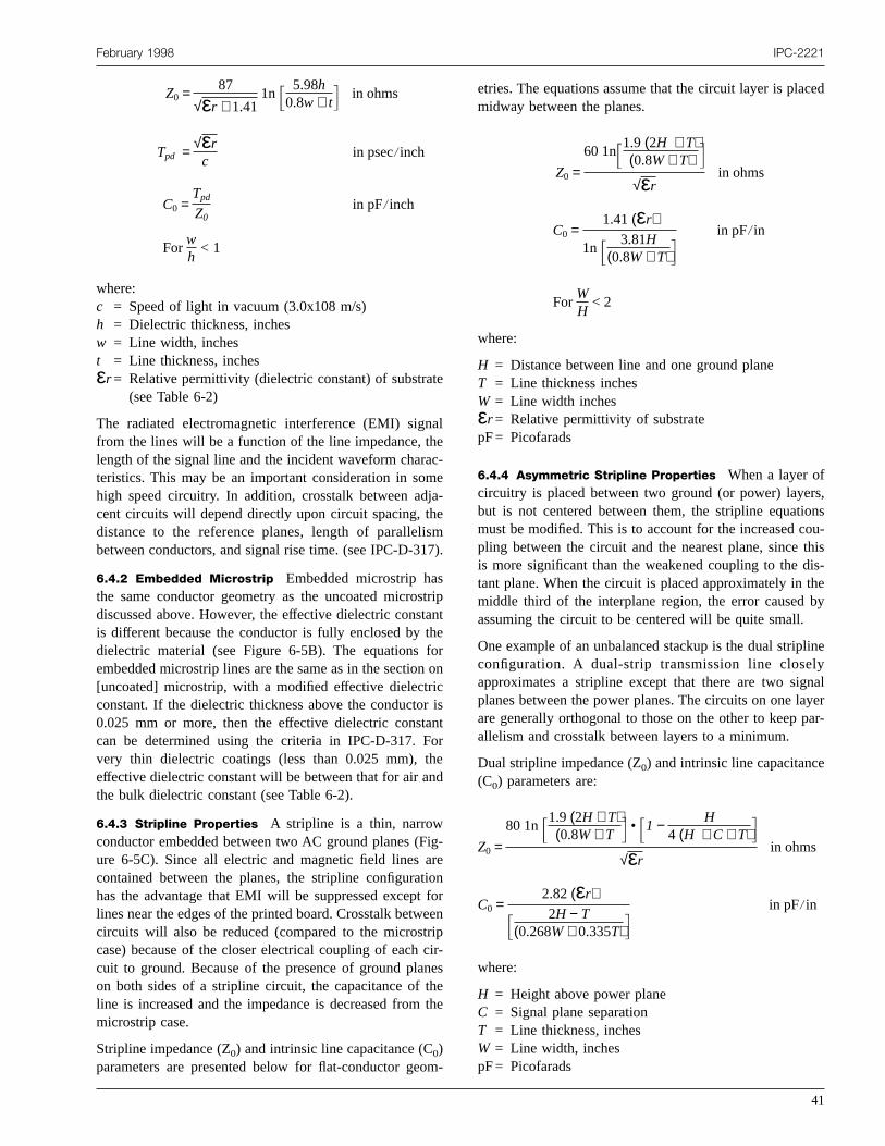
te
naheacmjaheis1
ssttathfonicranohn
Firtiofericnth
o
ced
s,nsu-thisis-heby
lineynalyerar-
February 1998 IPC-2221
Z0 = 87
√εr + 1.411n F 5.98h0.8w + tG in ohms
Tpd = √εrc
in psec/inch
C0 =TpdZ0
in pF/inch
Forwh< 1
where:c = Speed of light in vacuum (3.0x10⁸ m/s)h = Dielectric thickness, inchesw = Line width, inchest = Line thickness, inchesεr = Relative permittivity (dielectric constant) of substra
(see Table 6-2)
The radiated electromagnetic interference (EMI) sigfrom the lines will be a function of the line impedance, tlength of the signal line and the incident waveform charteristics. This may be an important consideration in sohigh speed circuitry. In addition, crosstalk between adcent circuits will depend directly upon circuit spacing, tdistance to the reference planes, length of parallelbetween conductors, and signal rise time. (see IPC-D-3
6.4.2 Embedded Microstrip Embedded microstrip hathe same conductor geometry as the uncoated microdiscussed above. However, the effective dielectric consis different because the conductor is fully enclosed bydielectric material (see Figure 6-5B). The equationsembedded microstrip lines are the same as in the sectio[uncoated] microstrip, with a modified effective dielectrconstant. If the dielectric thickness above the conducto0.025 mm or more, then the effective dielectric constcan be determined using the criteria in IPC-D-317. Fvery thin dielectric coatings (less than 0.025 mm), teffective dielectric constant will be between that for air athe bulk dielectric constant (see Table 6-2).
6.4.3 Stripline Properties A stripline is a thin, narrowconductor embedded between two AC ground planes (ure 6-5C). Since all electric and magnetic field lines acontained between the planes, the stripline configurahas the advantage that EMI will be suppressed exceptlines near the edges of the printed board. Crosstalk betwcircuits will also be reduced (compared to the microstcase) because of the closer electrical coupling of eachcuit to ground. Because of the presence of ground plaon both sides of a stripline circuit, the capacitance ofline is increased and the impedance is decreased frommicrostrip case.
Stripline impedance (Z0) and intrinsic line capacitance (C0)parameters are presented below for flat-conductor ge
l
-e-
m7).
ripnteron
istred
g-enorenpir-esethe
m-
etries. The equations assume that the circuit layer is plamidway between the planes.
Z0 =60 1nF1.9 (2H + T)
(0.8W+ T) G√εr in ohms
C0 =1.41(εr)
1n F 3.81H(0.8W+ T)G
in pF/in
ForWH< 2
where:
H = Distance between line and one ground planeT = Line thickness inchesW = Line width inchesεr = Relative permittivity of substratepF= Picofarads
6.4.4 Asymmetric Stripline Properties When a layer ofcircuitry is placed between two ground (or power) layerbut is not centered between them, the stripline equatiomust be modified. This is to account for the increased copling between the circuit and the nearest plane, sinceis more significant than the weakened coupling to the dtant plane. When the circuit is placed approximately in tmiddle third of the interplane region, the error causedassuming the circuit to be centered will be quite small.
One example of an unbalanced stackup is the dual stripconfiguration. A dual-strip transmission line closelapproximates a stripline except that there are two sigplanes between the power planes. The circuits on one laare generally orthogonal to those on the other to keep pallelism and crosstalk between layers to a minimum.
Dual stripline impedance (Z0) and intrinsic line capacitance(C0) parameters are:
Z0 =80 1nF1.9 (2H + T)
(0.8W+ T G • F1 − H4 (H + C + T)G
√εr in ohms
C0 =2.82(εr)
F 2H − T(0.268W+ 0.335T)G
in pF/in
where:
H = Height above power planeC = Signal plane separationT = Line thickness, inchesW = Line width, inchespF= Picofarads
41
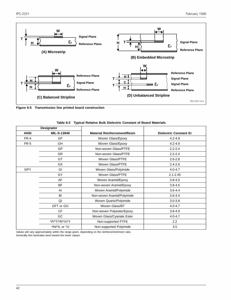
IPC-2221 February 1998
IPC-2221-6-5
Figure 6-5 Transmission line printed board construction
Signal Plane
Reference Plane
Signal Plane
Reference Plane
Reference Plane
Signal Plane
Signal Plane
Reference Plane
Reference Plane
Signal Plane
(A) Microstrip
W
H
H
H
T
(B) Embedded Microstrip
(C) Balanced Stripline
TH
W
W
T
T
W
H
C
(D) Unbalanced Stripline
Reference Plane
▼
▼▼▼
▼▼
T
▼▼
▼▼
▼▼
▼▼
▼
▼
▼
▼
H
▼
▼
εr
εrεr
εr
▼▼
▼▼
▼
▼
▼
▼
▼
▼
▼
▼▼
▼ H
Table 6-2 Typical Relative Bulk Dielectric Constant of Board Materials
Designator
Material Reinforcement/Resin Dielectric Constant ErANSI MIL-S-13949
FR-4 GF Woven Glass/Epoxy 4.2-4.9
FR-5 GH Woven Glass/Epoxy 4.2-4.9
GP Non-woven Glass/PTFE 2.2-2.4
GR Non-woven Glass/PTFE 2.2-2.4
GT Woven Glass/PTFE 2.6-2.8
GX Woven Glass/PTFE 2.4-2.6
GPY GI Woven Glass/Polyimide 4.0-4.7
GY Woven Glass/PTFE 2.1-2.45
AF Woven Aramid/Epoxy 3.8-4.5
BF Non-woven Aramid/Epoxy 3.8-4.5
AI Woven Aramid/Polyimide 3.6-4.4
BI Non-woven Aramid/Polyimide 3.6-4.4
QI Woven Quartz/Polyimide 3.0-3.8
GFT or GIJ Woven Glass/BT 4.0-4.7
CF Non-woven Polyester/Epoxy 3.8-4.9
GC Woven Glass/Cyanate Ester 4.0-4.7
*P/*T/*R/*X/*Y Non-supported PTFE 2.2
*IN/*IL or *IJ Non-supported Polyimide 3.5
Values will vary approximately within the range given, depending on the reinforcement/resin ratio.Generally thin laminates tend toward the lower values.
42
e,s
e
uignatar
isss
uoe
nee.
yeitesua.5ciian
proreymn
Fig--thlines toC
aato-omeseunduc-
heur-p-cir-emesehates,itornotthe
viammhe
alsoci-for
February 1998 IPC-2221
This stackup is shown in Figure 6-5D. As with striplinEMI will be completely shielded except for signal linenear the edges of the printed board.
The above equations can be adapted to determine Z0 or C0for asymmetric stripline circuits that are not dual striplinPlane sequences for a four-layer board should bedescribed in Figure 6-5D. For boards with more than folayers, the sequence should be arranged so that the slayers are symmetrical about the ground or voltage plaThis may be accomplished several ways provided thatadjacent signal layers, not separated by a ground or volplane should have their key axes running perpendiculaeach other. For 6-layer board, the sequence might be:
ASignal #1Plane #1Signal #2Signal #3Plane #2Signal #4
or
BSignal #1Signal #2Plane #1Plane #2Signal #3Signal #4
‘‘A’’ is the desired configuration since the impedancewell matched through the entire stack-up. ‘‘B’’ is a ledesirable configuration since signals 1 and 4 will havemuch higher impedance than signals 2 and 3.
Special attention is required in the design of specific circcharacteristics where attention must be given to total cductor lengths, both short and long conductor runs, as was total interconnection routing.
DC power and ground planes also function as AC refereplanes. Power and ground connector pins should be evdistributed along the edge of the board for AC referenc
As a general rule, the reference planes of a multilaprinted board design should not be segmented. Limplane segmentation, in which the segmented plane isported by an elevated plane to an adjacent signal layer,supported by plated-through holes on approximately 2mm centers on both sides, may be used to ‘‘bury’’ a spehigh frequency signal within the planes to create a ‘‘coaxtype’’ line within the board. Spacing of the holes is depedent on frequency of the signal.
6.4.5 Capacitance Considerations Figures 6-6 and 6-7show the intrinsic line capacitance/per unit length, of coper, for microstrip and stripline, respectively. These chaprovide capacitance in pF/ft for 1 oz. copper conductwith various dielectric thicknesses to the ground or powreference plane. Figure 6-7 for stripline is based upon smetry with the conductor centered between the refereground and power planes.
.asrnale.nygeto
a
itn-ll
cenly
rdp-nd4all-
-tssr-ce
The capacitance associated with single crossover (seeure 6-8) is very small and is typically a fraction of a picofarad. As the number of crossovers per unit lengincreases, the intrinsic capacitance of the transmissionalso increases. The crossover lumped capacitance addthe intrinsic line capacitance. Crossover capacitance (c)may be approximated by:
Cc = Xεr(l + 0.8h)(W+ 0.8h)
hin pF
provided thatl ≥ 0.5h
W≥ 0.5h
where:
X = 0.0089 ifh, l andW are in mm, 0.225 ifh, l andWare in inches
εr = relative permittivityh = dielectric thickness between crossoversl = lengthW = Width
6.4.6 Inductance Considerations Inductance is theproperty of a conductor that allows it to store energy inmagnetic field induced by a current flowing through thconductor. When this current has high frequency compnents, the self-inductance of the leads and traces becsignificant, leading to transient or switching noise. Thetransients are related to the inductance of a power/groloop and the circuit must be designed to reduce this indtance as much as possible.
A common technique to reduce this switching noise is tuse of decoupling capacitors that serve to provide the crent from a point closer to the IC gate than the power suply. Even when these capacitors are designed into thecuit, the positioning of the capacitor is important. If thcapacitor leads are too long, the self inductance becotoo high leading to switching noise. Decoupling on thboards is normally achieved with discrete capacitors tcan be closely positioned to the IC. In higher I/O packaga trend has begun which places the decoupling capacinside of the package. This has the double advantage ofusing real estate for the capacitor location and reducingsize of the capacitor interconnections.
Another consideration is the use of smaller diameterholes and their associated pad sizes. A change from 0.5vias to 0.3 mm vias will reduce parasitic inductance in tcircuit. Smaller diameter vias will improve it even more.
Closely spaced adjacent power and ground planes arebeing utilized to provide high frequency decoupling capatance. This also decreases the real estate requireddecoupling capacitors.
43
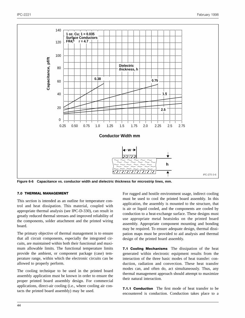
IPC-2221 February 1998
IPC-275-3-6
Figure 6-6 Capacitance vs. conductor width and dielectric thickness for microstrip lines, mm.
0
20
40
60
80
100
120
140
0.25 0.50 0.75 1.0 1.25 1.5 1.75 2.0 2.25 2.5 2.75
1 oz. Cu; 1 = 0.035 Surface Conductors FR4, r = 4.7ε
0.38
Dielectric thickness, h
0.75
1.5
2.5
Ca
pa
cit
an
ce
, p
f/ft
Conductor Width mm
h
w
▼
▼
▼
▼
ontht ioin
rir-i-smbe
rdthian-
gisatyustrdgssi-al
en-ernyize
a
7.0 THERMAL MANAGEMENT
This section is intended as an outline for temperature ctrol and heat dissipation. This material, coupled wiappropriate thermal analysis (see IPC-D-330), can resulgreatly reduced thermal stresses and improved reliabilitythe components, solder attachment and the printed wirboard.
The primary objective of thermal management is to ensuthat all circuit components, especially the integrated ccuits, are maintained within both their functional and maxmum allowable limits. The functional temperature limitprovide the ambient, or component package (case) teperature range, within which the electronic circuits canallowed to properly perform.
The cooling technique to be used in the printed boaassembly application must be known in order to ensureproper printed board assembly design. For commercapplications, direct-air cooling (i.e., where cooling air cotacts the printed board assembly) may be used.
44
-
nfg
e
-
el
For rugged and hostile environment usage, indirect coolinmust be used to cool the printed board assembly. In thapplication, the assembly is mounted to the structure, this air or liquid cooled, and the components are cooled bconduction to a heat-exchange surface. These designs muse appropriate metal heatsinks on the printed boaassembly. Appropriate component mounting and bondinmay be required. To ensure adequate design, thermal dipation maps must be provided to aid analysis and thermdesign of the printed board assembly.
7.1 Cooling Mechanisms The dissipation of the heatgenerated within electronic equipment results from thinteraction of the three basic modes of heat transfer: coduction, radiation and convection. These heat transfmodes can, and often do, act simultaneously. Thus, athermal management approach should attempt to maximtheir natural interaction.
7.1.1 Conduction The first mode of heat transfer to beencountered is conduction. Conduction takes place to

February 1998 IPC-2221
IPC-275-3-7
Figure 6-7 Capacitance vs. conductor width and spacing for striplines, mm.
1 oz Cu, FR4, ε r = 4.7Spacing, h = Separation Between stripline and Ground Plane
20
30
40
50
60
70
80
90
100
110
120
130
140
150
180
0.13 0.25 0.38 0.51 0.64 0.76 0.89 1.02 1.14 1.27 1.40 1.52 1.65 1.78 1.90
0.25
0.33
0.15
Spacing
0.75
1.00
1.25
Cap
acit
ance
/ft
(pF
)
Conductor Width
h
w
▼
▼
▼
▼
ofr-sstur
ro-the
at)eeniron-
the-he
noteriv-ofe.r-ce
varying degree through all materials. The conductionheat through a material is directly proportional to the themal conductivity constant (K) of the material, the crosectional area of the conductive path and the tempera
IPC-275-3-8
Figure 6-8 Single conductor crossover
Shaded Area Indicates Crossover
▼
▼▼
▼
▼
▼
▼Wh
l
e
difference across the material. Conduction is inversely pportional to the length of the path and the thickness ofmaterial (see Table 7-1).
7.1.2 Radiation Thermal radiation is the transfer of heby electromagnetic radiation, primarily in the infrared (IRwavelengths. It is the only means of heat transfer betwbodies that are separated by a vacuum, as in space envments.
Heat transfer by radiation is a function of the surface of‘‘hot’’ body with respect to its emissivity, its effective surface area and the differential to the forth power of tabsolute temperatures involved.
The emissivity is a derating factor for surfaces that are‘‘black bodies,’’ It is defined as the ratio of emissive powof a given body to that of a black body, for which emissity is unity (1.0). The optical color of a body has little tdo with it being a ‘‘thermal black body.’’ The emissivity oanodized aluminum is the same if it is black, red or bluHowever, surface finish is important. A matte or dull suface will be more radiant than a bright or glossy surfa(see Table 7-2).
45

IPC-2221 February 1998
Table 7-1 Effects of Material Type on Conduction
Materials
Thermal Conductivity (K)
Watts/m °C Gram-calorie/cm °C • s
Still Air 0.0276 0.000066
Epoxy 0.200 0.00047
Thermally Conductive Epoxy 0.787 0.0019
Aluminum Alloy 1100 222 0.530
Aluminum Alloy 3003 192 0.459
Aluminum Alloy 5052 139 0.331
Aluminum Alloy 6061 172 0.410
Aluminum Alloy 6063 192 0.459
Copper 194 0.464
Steel Low Carbon 46.9 0.112
oplo
ishe
idrap-
thonrisfaaion
eenttedonec-byispli-
ing
i-
if-a-ithn.
Devices, components, etc. close to one another will abseach others radiant energy. If radiation is to be the princimeans of heat transfer, ‘‘hot’’ spots must be kept cleareach other.
7.1.3 Convection The convection heat transfer modethe most complex. It involves the transfer of heat by tmixing of fluids, usually air.
The rate of heat flow by convection from a body to a fluis a function of the surface area of the body, the tempeture differential, the velocity of the fluid and certain proerties of the fluid.
The contact of any fluid with a hotter surface reducesdensity of the fluid and causes it to rise. The circulatiresulting from this phenomenon is known as ‘‘free’’ o‘‘natural’’ convection. The air flow can be induced in thmanner or by some external artificial device, such as aor blower. Heat transfer by forced convection can bemuch as ten times more effective than natural convect
Table 7-2 Emissivity Ratings for Certain Materials
Material and Finish Emissivity
Aluminum Sheet - Polished 0.040
Aluminum Sheet - Rough 0.055
Anodized Aluminum - any color 0.80
Brass - Commercial 0.040
Copper - Commercial 0.030
Copper - Machined 0.072
Steel - Rolled Sheet 0.55
Steel - Oxided 0.667
Nickel Plate - Dull Finish 0.11
Silver 0.022
Tin 0.043
Oil Paints - Any Color 0.92-0.96
Lacquer - Any Color 0.80-0.95
46
rbef
-
e
ns.
7.1.4 Altitude Effects Convection and radiation are thprinciple means by which heat is transferred to the ambiair. At sea level approximately 70% of the heat dissipafrom electronic equipment might be through convectiand 30% by radiation. As air becomes less dense, convtive effects decrease. At 5200 m the heat dissipatedconvection may be less than half that of radiation. Thneeds to be considered when designing for airborne apcations.
7.2 Heat Dissipation Considerations Design of multi-layer boards to remove heat from a high thermal radiatprinted board assembly should consider the use of:
• Heatsinking external planes (usually copper or alumnum);
• Heatsinking internal planes;
• Special heatsink fixtures;
• Connection to frame techniques;
• Liquid coolants and heatsink formation;
• Heat pipes; and
• Heatsinking constraining substrates.
7.2.1 Individual Component Heat Dissipation Heat-sinking of individual components can use a variety of dferent techniques. 8.1.10 of this standard provides informtion on some of the heatsinking devices that come windividual components requiring specific heat dissipatioIn addition, consideration should be given to:
• Heatsink mounting (hardware or soldering);
• Thermal transfer adhesives, paste, or other materials;
• Solder temperature requirements; and
• Cleaning requirements under heatsinks.

le
d
t
ur
ew
f
nnk
od
in
og
fanotOde
lenci1pe
anntirenbey
um-ngekrtsinans).ders(asbed
ase, theows
c-et isbe
fer.cann-q-os-
reink/ro-
ci-tedhe-nk
offndfin-tru-he-erughuf-uxwill
February 1998 IPC-2221
7.2.2 Thermal Management Considerations for BoardHeatsinks The following factors must be addressed whithe printed board components are being placed:
1. Method of heatsink mounting (i.e., adhesive bonrivet, screw, etc.) to printed board
2. Thickness of heatsink and printed board assemblyallow adequate component lead protrusion
3. Automatic component insertion clearances (see Fig7-1)
4. Heatsink material and material properties
5. Heatsink finish (i.e., anodize, chemical film, etc.)
6. Component mounting methods (i.e., spacers, scrbonding, etc.)
7. Heat transfer path and rate of heat transfer
8. Producibility (i.e., method of assembly, method ocleaning, etc.)
9. Dielectric material required between the heatsink aany circuitry that may be designed on the heatsimounting surface of the printed board
10. Edge clearance to any exposed circuitry (i.e., compnent pads and circuit runs) Tooling hole location ansize
11. Heatsink shape as it relates to the structure of heatsprinted board assembly
12. The heatsink should fully support the component. Dnot allow the component the opportunity to tip durinassembly or soldering.
Heatsinksshall be designed to avoid the occurrence omoisture traps and to allow access for post-soldering cleing. This can be accomplished by providing accessible slin the heatsink instead of round clearance holes under TTO66, and similar packages with leads which extenthrough the heatsink and are soldered into the printboard.
Through hole printed board assembly heatsinks generaare of a ladder configuration when standard componpackage types (i.e., DIPs and axial-leaded components)be used. The ladder heatsink type is preferred due torelative simplicity in design and fabrication. Figure 7-provides standard clearances between heatsink and comnents that are necessary to facilitate automatic componinsertion.
Certain printed board assemblies (e.g., power suppliesother analog designs in particular) utilize many differecomponent types. The circuit function for these analog ccuits may be very dependent upon component placemFor analog designs, heatsinks sometimes cannotdesigned in a ladder type configuration, however thshould be designed with producibility in mind. Minimizing
,
o
e
,
d
-
k/
-s3,
d
lytants
o-nt
d
-t.e
the number of unique cutout shapes required, and the nber of areas where the heatsink thickness must cha(requiring milling or lamination) will enhance heatsinproducibility. When machined heatsinks are used effoshould be made to utilize as large a radius as possiblecorners to enhance producibility (e.g., a 3.0 mm radius ccost substantially more to fabricate than a 6.0 mm radiuIn all cases, analog heatsink designs that can’t use ladshould be designed in parallel with the printed boardopposed to after completion of artwork) and shouldreviewed for producibility in both the metal fabrication anprinted board assembly areas.
7.2.3 Assembly of Heatsinks to Boards Assembly ofheatsinks to printed wiring boards may be accomplishedlisted below (in order of manufacturing preference). If thboard and the heatsink are purchased as an assemblymanufacturer may have other preferences. Table 7-3 shthe preferences.
Details of these assembly methods are as follows:
1. Mechanical Fasteners:Riveting is the preferred fas-tening method, but care must be taken in rivet seletion (solid or tubular), and rivet installation, to obviatlaminate damage. Screws should be used if the uniexpected to be disassembled. Closer contact maynecessary to resist vibration or improve heat transUse of adhesives along with mechanical fastenerspromote warpage but may help in a vibration enviroment. Dry film epoxy adhesives are preferred over liuids. Bonding temperatures should be as low as psible to minimize warpage.
2. Film Type Adhesives:Sheet adhesive is die omechanically cut to fit the outline of the heatsink. Thassociated cure cycles and warpage of the heatsprinted board assembly are problems that affect pducibility. See 4.2.3 for film type adhesives.
3. Liquid Adhesives:Liquid adhesive is a producibilityconcern because of the difficulty in application assoated cure cycle and warpage of the heatsink/prinboard assembly. The recommended structural adsives listed in 4.2.2 are well suited for the heatsibonding application.
Specification of adhesive thickness involves a trade-between contact area (bond line) and producibility. Boline may be reduced by process variables (e.g., surfaceish or cleanliness), material warpage, and surface prosions (especially surface runs of 2 oz. copper). More adsive may improve contact, but excess can flow from undthe heatsink and contaminate lands and plated-throholes. In many cases, a 75% (of the heatsink) bond is sficient, but care must be taken to avoid moisture or flentrapment that cannot be cleaned. Adhesive bonding
47
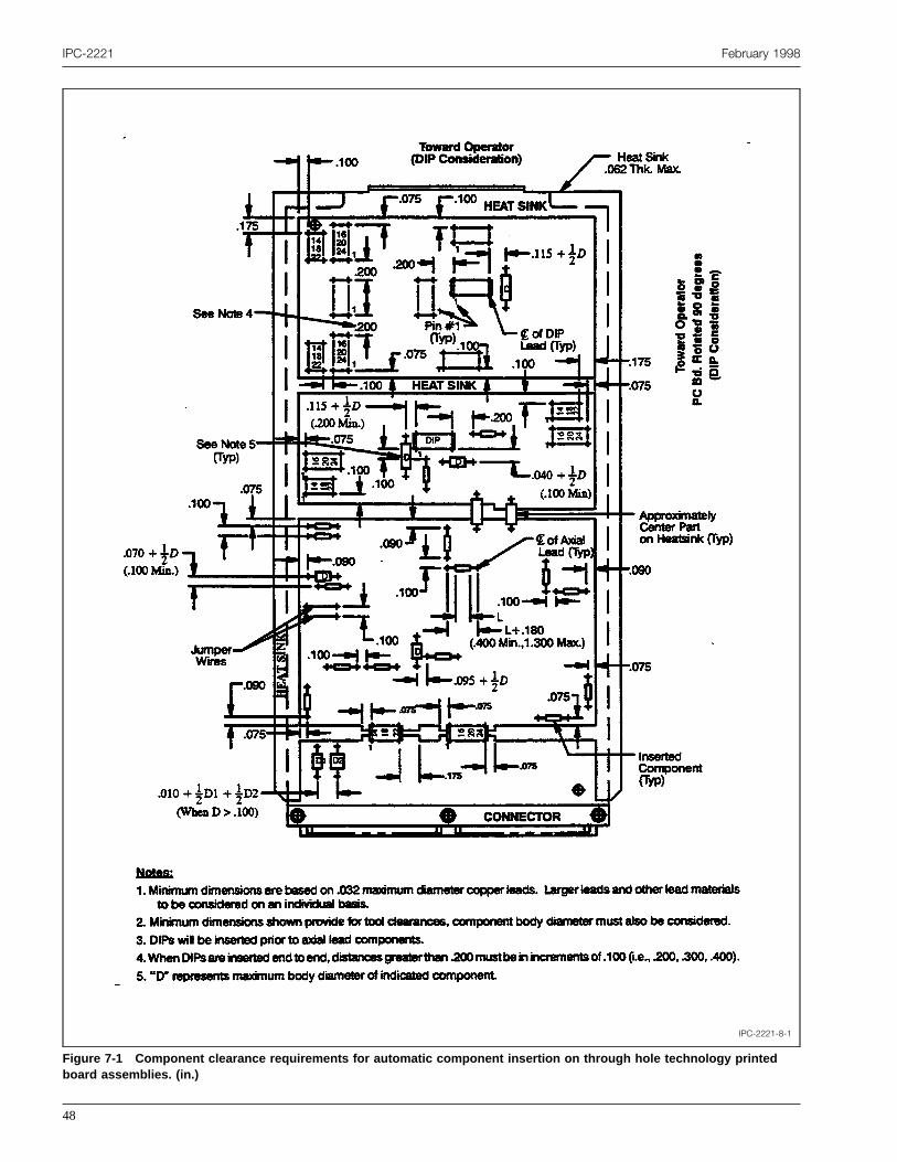
IPC-2221 February 1998
IPC-2221-8-1
Figure 7-1 Component clearance requirements for automatic component insertion on through hole technology printedboard assemblies. (in.)
48

February 1998 IPC-2221
Table 7-3 Board Heatsink Assembly Preferences
Method Major Advantages Major Disadvantages Considerations
Rivets Fastest, no cure cycle oradhesive application
Board area and holes neededfor rivets
Use standard rivet sizes
Screws Allows disassembly Requires washers and nuts,board area and holes
Use standard hardware
Film Adhesive No wasted space, potentiallyimproved heat transfer, highervibration natural frequency.Increased insulation
Cure time and possiblewarpage
Low cure temperature willminimize warpage
Liquid Adhesive No wasted space, potentiallyimproved heat transfer, highervibration natural frequency
Producibility concern as wellas cure time and warpageconcern
Low cure temperature willminimize warpage
ardnicahen
llyheuntighnvi-nvi-blyinkiron-to
itherr-olidon
dsiffere alidllowlec-ted
ondeg-theded.oftedizeandg thone
ageringomelete.
o-s antedheandeu-ht.ol--ard5 toforor
rialste-
ld or
uc-
ithpan-tedintmalng
ision
raise the vibration natural frequency of the printed boassembly above that which can be obtained by mechafasteners alone. Heat transfer may also be improved wadhesive bonding is used.
7.2.4 Special Design Considerations for SMT BoardHeatsinks Surface mount heatsinks can dramaticaaffect the coefficient of thermal expansion (CTE) of tsurface mount assembly. The reliability of surface mocomponent solder joints may be compromised if a hCTE material is used, but depends upon the service eronment of the surface mount assembly. Laboratory eronments which do not subject the surface mount assemto significant temperature changes may allow heatsmaterials such as 1100 aluminum to be used. Most envments require the use of low CTE heatsink materialsprovide long solder joint life.
Heatsinks used in surface mount applications are ebuilt within the printed board (typically copper-Invacopper layers laminated in the printed board) or are a splate that has a surface mount printed board bonded toor both sides.
Bonding of the heatsink to two printed wiring boarrequires a compliant sheet adhesive to decouple the dence in CTE of the heatsink and printed board and serva vibration damping and heat transfer material. A sosheet adhesive provides an inspectable material that athe assembler to check for pin holes that might allow etrical connection between the heatsink and the prinboard.
Silicone sheet adhesives have been very effective in bing printed boards to a solid heatsink. The bonding intrity of silicone sheet adhesives is dependent uponproper application of a primer to the surfaces to be bonCare must be taken to prevent silicone contaminationsurfaces which are to be soldered and/or conformal coaSee 4.2.2 for silicone sheet adhesives. To minimwarpage of the final bonded assembly, and thermalmechanical stress on the assembled components durinadhesive cure process, a low temperature curing silic
l
e
-s
s
-
.
e
adhesive should be chosen. Components subject to damshould be so noted on the drawing and protection duassembly required. It may be necessary to assemble scomponents by hand after the bonding process is comp
7.3 Heat Transfer Techniques
7.3.1 Coefficient of Thermal Expansion (CTE) Charac-teristics For applications with surface mount compnents, the CTE of the interconnecting structure becomeimportant consideration. Table 7-4 establishes calculareliability figures of merit related to the differences in tX and Y expansion characteristics of the componentthe substrates, the distance from the solder joint to the ntral point (zero strain point), and the solder joint heigThis factor is related to the total strain per cycle of the sder joint. It is important to minimize the relative differences in the CTE of the component and printed boassembly. Typical ceramic substrates have a CTE from7 ppm/°C. Figure 7-2 provides examples of the CTEsome materials used by themselves (polymide, glassepoxy glass) and some constraining substrate mateused in conjunction with the printed board dielectric marials.
7.3.2 Thermal Transfer Components, which for thermareasons require extensive surface contact with the boarwith a heatsink mounted on the board,shall be compatiblewith or protected from processing solutions at the condtive interface.
7.3.3 Thermal Matching A primary thermal concernwith through-hole mounted glass components and wceramic surface-mounted components is the thermal exsion mismatch between the component and the prinboard. This mismatch may result in fractured solder jointerconnections if the assembly is subjected to thershock, thermal cycling, power cycling and high operatitemperatures.
The number of fatigue cycles before solder joint failuredependent on, but not limited to, the thermal expans
49

IPC-2221 February 1998
Table 7-4 Comparative Reliability Matrix Component Lead/Termination Attachment
CyclicServices
Environment[°C]
Design Life [Years]
5 10 20
Cyclic Frequency [Cycles/Day]
0.1 1 10 0.1 1 10 0.1 1 10
Mean Cyclic Life Frequency [Cycles/Day]
183 1825 18,250 365 3650 36,500 730 7300 73,000
Relative Reliability Index, R [ppm/°C]
+20 to +40 2200 790 360 1600 580 270 1150 420 200
+20 to +80 670 240 110 490 170 79 350 130 58
-40 to +401 600 230 110 440 170 83 330 130 62
-40 to 801 370 140 65 270 100 48 200 75 36(1) These environments straddle the transition region from stress-driven (<20°C) to strain/creep-driven (>+20°C); for such
environments it has been shown that fatigue occurs significantly earlier by a mechanism different from that underlying thisreliability matrix and it should be assumed that the R-values for these environments are optimistic.
ardusentherfer-
thee oreedayowngesC)f 5atin
, thexinlife.fordifillisareteme
s,m-unasethelde
vertheon,
anonuc-fab-dctsnifi-
ereignfol-andra-
nt
ire-
and
b-
.
mismatch between the component and the printed bothe temperature excursion over which the assembly moperate, the solder joint size, the size of the componand the power cycling that may cause an undesirable tmal expansion mismatch if a significant temperature difence exists between the component and the board.
7.4 Thermal Design Reliability Design life can be veri-fied through comparative testing intended to simulateservice environment. Table 7-4 represents an exampldesign verification of surface mounted devices for thservice environments: 0.1 cycles per day, 1 cycle perand 10 cycles per day. The service environments shrepresent four categories of different temperature ranThe table establishes a relative reliability index (ppm/°for the design depending on a desired equipment life o10, or 20 years. This reliability index (R) is a factor thmay be used in considering if the assembly will survivethe environment for the expected life.
The longer the life or the more severe the requirementslower the number in the matrix becomes. A reliability indroughly gives the maximum cyclic strain that will resulta mean fatigue life just equal to the expected designThe matrix is primarily meant for leadless components;leaded components, some underlying relationships areferent which, while not changing the indicated trends, wchange the matrix quantitatively. Only mean cyclic liferepresented, indicating when half the componentsexpected to fail, not when the first component in a sysfails. The statistical distribution of the solder joint fatigufailure has to be included in a reliability assessment.
In the case of through-hole mounted glass componentis often sufficient to provide stress-relief bends in the coponent’s leads (see section 8.1.14). With surface-mocomponents, the number of fatigue cycles can be increby reducing the thermal expansion mismatch, reducingtemperature gradient, increasing the height of the so
50
,t,-
f
,
.
,
e
-
it
td
r
joint, using the smallest physical size component wherepossible, and by optimizing the thermal path betweencomponent and the board. For more detailed informatisee IPC-D-279 and IPC-SM-785.
8.0 COMPONENT AND ASSEMBLY ISSUES
The mounting and attachment of components playimportant role in the design of a printed board. In additito their obvious effect on component density and condtor routing, these aspects of board design also impactrication, assembly, solder joint integrity, repairability antesting. Therefore, it is important that the design refleappropriate tradeoffs that recognize these and other sigcant manufacturing considerations.
All componentsshall be selected so as to withstand thvibration, mechanical shock, humidity, temperatucycling, and other environmental conditions the desmust endure when the components are installed. Thelowing are requirements the designer should considerdetail on the assembly drawing in specific notes or illusttions.
As a minimum, component mounting and attachmeshould be based on the following considerations:
• Electrical performance and electrical clearance requments of the circuit design.
• Environmental requirements.
• Selection of active and passive electronic componentsassociated hardware.
• Size and weight.
• Minimizing of heat generation and heat dissipation prolems.
• Manufacturing, processing and handling requirements
• Contractual requirements.
• Serviceability requirements.
• Equipment usage and useful life.
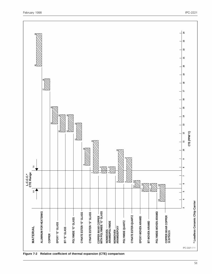
February 1998 IPC-2221
IPC-2221-7-1
Figure 7-2 Relative coefficient of thermal expansion (CTE) comparison
MA
TE
RIA
L
L.C
.C.C
.*
CT
E R
ang
e
COPP
ER
EPO
XY ‘‘
E’’ G
LASS
POLY
IMID
E ‘‘E
’’ G
LASS
COPP
ER IN
VAR
COPP
ER
WIT
H PO
LYIM
IDE
‘‘E’’
GLA
SS
POLY
IMID
E Q
UART
Z
ALUM
INUM
FO
R HE
ATSI
NKS
EPO
XY-W
OVE
N AR
AMID
BT-W
OVE
N AR
AMID
COPP
ER IN
VAR
COPP
ER
12.5
/75/
12.5
CTE
(PPM
/°C)
1718
1513
BT-‘‘
E’’ G
LASS
1412
1412
CYNA
TE E
STER
-‘‘E’
’ GLA
SS
1311
CYNA
TE E
STER
-‘‘S’
’ GLA
SS
108
117
6.3
5.7
CYNA
TE E
STER
-QUA
RTZ
5.0
6.0
POLY
IMID
E-W
OVE
N AR
AMID
5.0
6.0
5.5
3.8
34
56
78
910
1112
1314
1516
1718
1920
2122
2324
106
2420
96
NONW
OVE
N AR
AMID
/EPO
XY
NONW
OVE
N AR
AMID
/PO
LYIM
IDE
87
87
5.5
7.5
▼
▼
* L
ead
less
Cer
amic
Ch
ip C
arri
er
51

en
fte
teraintbl
ereluse
bteor-ostoca-
rpothly dset angconev
-ndntsfla
theledymac-
o
beed.
orm-pro-
thebeed
to
ee
dire
nt’sreaopeentisse
by
tedc-
y ber-
ialthe
o-the
n-ns,art., all
en-.05h asbutugh
IPC-2221 February 1998
• Automatic insertion and placement requirements, whthese methods of assembly are to be used.
• Test methods to be employed before, during and aassembly.
• Field repair and maintenance considerations.
• Stress relief.
• Adhesive requirements.
8.1 General Placement Requirements
8.1.1 Automatic Assembly When automatic componeninsertion and attachment is employed, there are sevprinted board design parameters that must be takenaccount that are not applicable when manual assemtechniques are used.
8.1.1.1 Board Size The size of the printed board to bautomatically assembled can vary substantially. Therefomanufacturers’ equipment specifications should be evaated with respect to the finished board requirements (5.3.3).
Standardization of automatic assembly operations canachieved through standard fixtures that can accommodavariety of board sizes or assembling boards in panel fmat. Using the panel assembly concept requires clcooperation with the printed board manufacturer in orderestablish tooling concepts, tool hole location, board lotion, coupon and fiducial locations.
8.1.1.2 Mixed Assemblies Automatic processes used foboth surface mounted and through-hole mounted comnents require special design considerations in order thatcomponents assembled in the first phase of the assembnot interfere with insertion heads during the second phaComponent placement should consider the stresses thaput on the board with insertion equipment, by isolatiparts wherever possible to specific areas so that the sephase insertion/placement stresses do not impact prously soldered connections.
8.1.1.3 Surface Mounting Automatic assembly considerations for surface mounted components include pick-aplace machines used to place/position chip componediscrete chip carriers, small outline packages, andpacks.
Special orientation symbols should be incorporated intodesign to allow for ease of inspection of the assembsurface mounted part. Techniques may include special sbols, or special land configurations to identify such charteristics as a lead of an integrated circuit package.
8.1.2 Component Placement Whenever possible,through-hole parts and components should be mounted
52
r
loy
,-e
ea
e
-eo.re
di-
-,t
-
n
the side of the printed board opposite that which wouldin contact with the solder, if the board is machine solder
Intermixing of through-hole and surface mount parts,mounting parts on both sides of the board, requires coplete understanding of the assembly and attachmentcesses (see IPC-CM-770 and IPC-SM-780).
Whenever possible, if their leads are dressed throughholes, axial and non-axial-leaded components shouldmounted per IPC-CM-770 on only one side of the printboard assembly.
Unless a component or part is specifically designedaccept another part into its configuration, thereshall be nostacking (piggybacking) of components or parts (sJ-STD-001).
Component leadsshall either be surface mounted, mountein through-holes, or mounted to terminals. Lead and wterminationsshall be soldered or wire bonded.
The variations in the actual placement of the componeleads into plated-through holes or on the termination ain addition to the tolerances on the component’s envel(body and leads) will cause movement of the componbody from the intended nominal mounting location. Thmisregistrationshall be accounted for such that worst caplacement of componentsshall not reduce their spacing toadjacent printed wiring or other conductive elementsmore than the minimum required electrical spacing.
If a component is bonded to the surface of the prinboard utilizing an adhesive (structural or thermally condutive), the placement of the componentshall consider thearea of adhesive coverage such that the adhesive maapplied without flowing onto or obscuring any of the teminal areas. Part attachment processesshall be specifiedwhich control the quantity and type of bonding matersuch that the parts are removable without damage toprinted board assembly. The adhesive usedshall be com-patible with both the printed board material, the compnent, and any other parts or materials in contact withadhesive.
Thermal concerns, functional partitioning, electrical cocerns, packing density, pick-and-place machine limitatiowave soldering holder concerns, vibration concerns, pinterference concerns, ease of manufacture and test, etcaffect the parts placement.
Parts should be placed on a 0.5 mm placement grid whever possible. When a 0.5 mm grid is not adequate, a 0mm placement grid should be used. Certain parts (sucsome relays) have leads that are not on standard gridsotherwise the parts should be placed so that the throholes are on grid.

tricthinnotg os tosten
esunth
s ter
eant
edlyblforidthaningbes nrd
ardiso
f thpoensidinardce
thes oge
(in
entethe
ofedre-odtedr-eingrendght
rdtser
po-edueofdi-
l-beerthepti-
ofofretorili-ithngu-’ee
enter
v-doto.
February 1998 IPC-2221
If equipment or other constraints do not allow for a megrid, parts may be on 0.100 in. placement grid. Whenis not adequate, a 0.050 in. grid may be used or eve0.025 in. grid. The 0.100 in. placement grid facilitatesonly parts insertion but also standard bed-of-nails testinthe board and of the assembly. If bed-of-nails testing ibe used (including in-circuit printed board assembly teing), the test fixturing becomes much more difficult whcomponents are placed off grid.
Figure 7-1 illustrates the producibility design allowancfor automatic component insertion. Through hole moprinted boards should observe component to edge ofboard spacing constraints on two (2) opposite edgeallow direct insertion into wave solder fingers. Othdesigns will require fixturing.
Both component heatsink considerations and board hsink requirements must be addressed in parts placeme
If the printed board assembly will not be tested with a bof-nails testing then the assembly grid will be limited onby the assembly machinery. If the printed board assemis testable with a bed-of-nails scheme, a 0.100 in. gridplated through hole spacing is preferred. A 0.075 in. gallows greater design density and is not a concern withassembly machinery but is a concern with bare boardcompleted assembly testing if a bed-of-nails testapproach is utilized. Bare board testing will normallydone at the printed board supplier and there presently icost penalty for off grid nor reduced grid printed boatesting.
The designer should allow sufficient component to boedge separation for test and assembly processes. If thnot possible, the designer should consider adding a remable section of board (i.e., breakaway tab). The edge ocomponent is defined as the physical edge of the comnent on sides where no leads protrude from the componand the edge of the surface land pattern for the leadedof a component. Preferably, components should be a mmum of 1.5 mm from the edge of the board and boguide or mounting hardware to allow for component plament, soldering, and test fixturing.
Components should not be grouped in such a way thatshadow one another during soldering. Do not align rowcomponents perpendicular to the direction of travel; stagthem.
Component polarities should be oriented consistentlythe same direction) throughout a given design.
For wave soldered surface mount chip types, componshould be bonded to the printed board prior to automasoldering with an adhesive specially formulated forpurpose.
sa
f
-
teo
t-.
-
yr
ed
o
isv-e-t,ei-
-
yfr
tsd
Specific requirements for part mounting are functionsthe type of component, the mounting technology selectfor the printed board assembly, the lead bending requiments for the component, the lead stress relief methselected, and placement of the components (either mounover surfaces without exposed circuitry, over protected sufaces, or over circuitry). Additional requirements ardependent upon the thermal requirements (the operattemperature environment, maximum junction temperaturequirements, and the component’s dissipated power), athe mechanical support requirements (based on the weiof the component).
Mounting methods for components of the printed boaassemblyshall be selected so that the final assembly meeapplicable vibration, mechanical shock, humidity, and othenvironmental conditions. The componentsshall bemounted such that the operating temperature of the comnent does not reduce the component’s life below requirdesign limits. The selected component mounting techniqshall ensure that the maximum allowable temperaturethe board material is not exceeded under operating contions.
8.1.3 Orientation Components should be mounted paralel to the edges of the printed board. They should alsomounted parallel or perpendicular to one another in ordto present an orderly appearance. When appropriate,component should be mounted in such a manner as to omize the flow of cooling air.
Assemblies are usually flow soldered with the top edgethe board in the lead (perpendicular to the directiontravel through the wave), mounting flanges and hardwaagainst the fixture or conveyor fingers, and edge conneclast. Surface mount components should be placed to factate solder flow in the wave. Rectangular components (wsolder caps at the ends) should be oriented with the loaxis parallel to the leading edge of the board, perpendiclar to the direction of travel. This avoids the ‘‘shadow’effect, where the body of the component would otherwisprevent free flow of solder to the trailing solder joint. SeFigure 8-1.
8.1.4 Accessibility Electronic componentsshall belocated and spaced so that the lands for each componare not obscured by any other component, or by any othpermanently installed parts. Each componentshall becapable of being removed from the assembly without haing to remove any other component. These requirementsnot apply to assemblies manufactured with no intentrepair (throw away assemblies) or as specified in 8.2.13
53
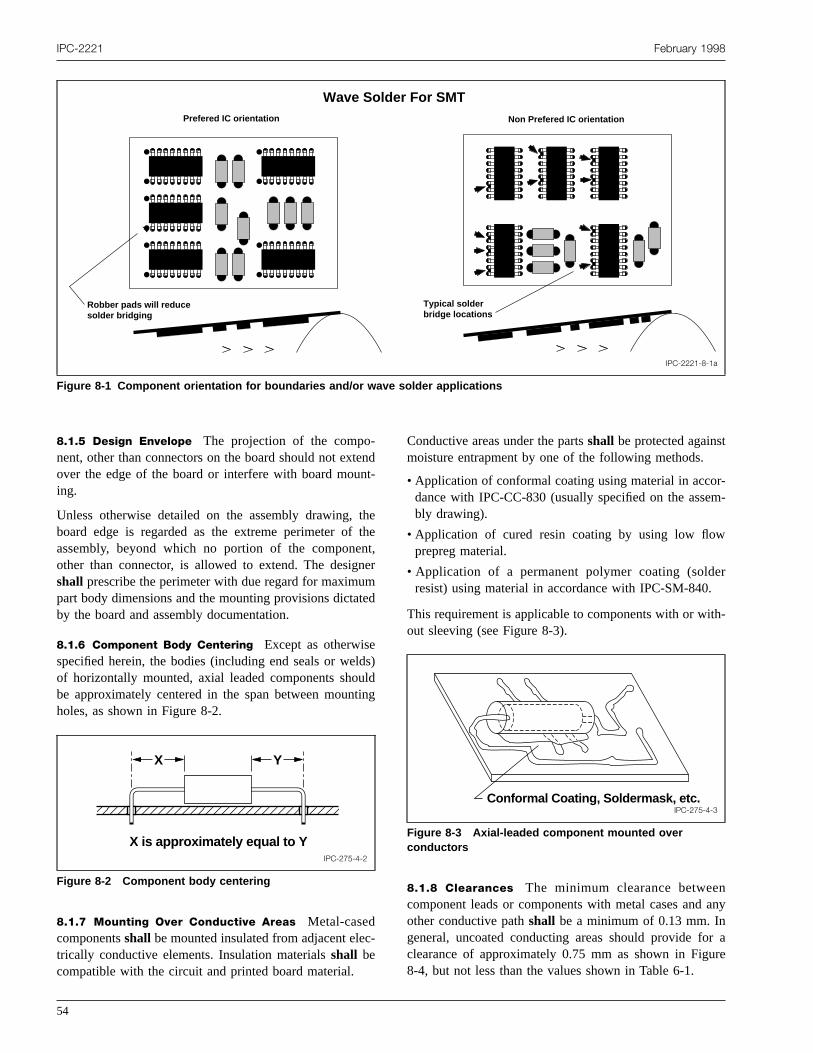
�
IPC-2221 February 1998
IPC-2221-8-1a
Figure 8-1 Component orientation for boundaries and/or wave solder applications
Wave Solder For SMTPrefered IC orientation
Robber pads will reduce solder bridging
Typical solder bridge locations
▼
▼
Non Prefered IC orientation
tennt
ththntnemte
ldsuldtin
c-
--
r
-
ny
are
8.1.5 Design Envelope The projection of the compo-nent, other than connectors on the board should not exover the edge of the board or interfere with board mouing.
Unless otherwise detailed on the assembly drawing,board edge is regarded as the extreme perimeter ofassembly, beyond which no portion of the componeother than connector, is allowed to extend. The desigshall prescribe the perimeter with due regard for maximupart body dimensions and the mounting provisions dictaby the board and assembly documentation.
8.1.6 Component Body Centering Except as otherwisespecified herein, the bodies (including end seals or weof horizontally mounted, axial leaded components shobe approximately centered in the span between mounholes, as shown in Figure 8-2.
8.1.7 Mounting Over Conductive Areas Metal-casedcomponentsshall be mounted insulated from adjacent eletrically conductive elements. Insulation materialsshall becompatible with the circuit and printed board material.
IPC-275-4-2
Figure 8-2 Component body centering
���X Y
X is approximately equal to Y
54
d-
ee,r
d
)
g
Conductive areas under the partsshall be protected againstmoisture entrapment by one of the following methods.
• Application of conformal coating using material in accordance with IPC-CC-830 (usually specified on the assembly drawing).
• Application of cured resin coating by using low flowprepreg material.
• Application of a permanent polymer coating (solderesist) using material in accordance with IPC-SM-840.
This requirement is applicable to components with or without sleeving (see Figure 8-3).
8.1.8 Clearances The minimum clearance betweencomponent leads or components with metal cases and aother conductive pathshall be a minimum of 0.13 mm. Ingeneral, uncoated conducting areas should provide forclearance of approximately 0.75 mm as shown in Figu8-4, but not less than the values shown in Table 6-1.
IPC-275-4-3
Figure 8-3 Axial-leaded component mounted overconductors
Conformal Coating, Soldermask, etc.

oa
thaa
d
5
ad.engethicigt
aeje
m
ds,eenpe-nose
perhe
February 1998 IPC-2221
Parts and componentsshall be mounted such that they dnot obstruct solder flow onto the topside termination areof plated through-holes.
8.1.9 Physical Support Dependent upon weight and heageneration characteristics, components weighing less t5 grams per lead which dissipate less than 1 watt, andnot clamped or otherwise supportedshall be mounted withthe component body in intimate contact with the printeboard as is practical, unless otherwise specified.
8.1.9.1 Component Mounting Techniques for Shock andVibration Axial-leaded components weighing less thangrams per leadshall be mounted with their bodies in inti-mate contact with the board. Dimensional criteria for lebending and spacingshall be as specified in Figure 8-9Axial-leaded components weighing 5 grams or more plead should be secured to the board utilizing mounticlamps. If clamps are not practical due to density considations, other techniques should be employed such thatsolder connections are not the only means of mechansupport. These techniques are used for components weing more than 5 grams when high vibration requiremenmust be met. (See 5.2.7 and Figures 8-5 and 8-6.)
When mounting chip components on edge, if the verticdimension is greater than the thickness dimension, thchip components should not be used in assemblies subto high vibration or shock loads. Vertical mountingshall beused for:
a) Low and tall profile SMDs with reflow terminationpads located in a single base surface;
b) Non-axial-leaded devices with leads egressing frotwo or more sides of the device(s); and
c) Non-axial-leaded devices with leads egressing fromsingle base surface.
s
nre
r
r-ealh-s
lnct
a
For radial leaded components with three or more leasuch as transistors, that require the use of spacers betwtheir base and the board surface for vertical mounting, scial attention should be given to ensuring that there ismovement of the spacer during vibration that might caudamage to surface conductors.
8.1.9.2 Class 3 High Reliability Applications Freestanding components weighing more than 5.0 gramsleadshall be mounted with the base surface paralleling tsurface of the board (see Figure 8-7). The componentshallbe supported on either:
IPC-275-4-5
Figure 8-5 Clamp-mounted axial-leaded component
Positive Displacement
Clamp
Secure Clamp to Board
▼
▼
IPC-275-4-6
Figure 8-6 Adhesive-bonded axial-leaded component
RTV Type Potting
Material
▼
IPC-275-4-4
Figure 8-4 Uncoated board clearance
Washer or other mechanical hardware
Spacing less than electrical clearance requirements
Not Recommended
Spacing less than electrical clearance requirements
Recommended
Spacing between printed wiring and mechanical hardware is 0.75 mm or more, but not less than allowed electrical clearance.
0.75 mm or more
������
��������
55

e
es
teden
beireid-7C.
baisuetedther-dt o
th
f-noa
anoiale
theea
ea-or
Toth-f
tor’s
ortheub-re,begn.
ir
notdsrheld
bear-pa-u-ted
inns
IPC-2221 February 1998
• Feet or standoffs integral to the component body (sFigure 8-7A and B);
• Specially configured non-resilient footed standoff devic(see Figure 8-7C); or
• Separate non-footed standoffs which do not block plathrough-holes nor conceal connections on the componside of the board.
Standoffs, footed or non-footed, are intended tomounted flush to the surface of the board. For this requment, a button standoff as shown in Figure 8-7B is consered a foot. Footed standoffs, as illustrated in Figures 8and 8-7D,shall have a minimum foot height of 0.25 mm
When a separate footed standoff device or separatenon-footed standoff is utilized and the componentmounted with the base surface paralleling the board sface, mounting should be such that the component basseated in contact with, and flat to, the footed or non-foostandoff. Mounting should also be such that the feet offooted standoff maintain full contact with the board suface. No standoffshall be inverted, tilted, or canted, anshould not be seated with any foot (or base surface) oucontact with the board or conductors thereon. Neithershallthe component be tilted, canted nor separated frommating surface of the resilient standoff device.
8.1.10 Heat Dissipation Design for heat dissipation ocomponentsshall insure that the maximum allowable temperature of the board material and the component isexceeded under operating conditions. Heat dissipation mbe accomplished by requiring a gap between boardcomponent, using a clamp or thermal mounting plate,attaching a compatible thermally-conductive materworking in conjunction with a thermal bus plane to thcomponent. (See Figure 8-8 for examples.)
Any heat dissipation technique or deviceshall permitappropriate cleaning to remove contaminants fromassembly. Conductive materials used to transfer h
56
e
t
--
se
r-is
f
e
tydr
t
between parts and heatsinkshall be compatible withassembly and cleaning processes.
Components on Class 3 assemblies which for thermal rsons require extensive surface contact with the boardwith a heatsink mounted on the board,shall be protectedfrom processing solutions at the conductive interface.prevent risk of entrapment, compatible materials and meods shall be specified to seal the interface from entry ocorrosive or conductive contaminants.
Note:Even totally nonmetallic interfaces that are proneentrap fluids can have adverse effects on the fabricatoability to pass required cleanliness tests.
8.1.11 Stress Relief Lands and terminalsshall belocated by design so that components can be mountedprovided with stress relief bends in such a manner thatleads cannot overstress the part lead interface when sjected to the anticipated environments of temperatuvibration, and shock. Where the lead bend radius cannotin accordance with Figure 8-9 in order to achieve desigoals, the bendsshall be detailed on the assembly drawing
The leads of components mounted horizontally with thebodies in direct contact with the printed boardshall bemounted with a method that ensures that stress relief isreduced or negated by solder fill in the lead bends. Leashall not be formed at the body of the component obetween the body of a component and any lead weld. Tleadshall extend straight from the body seal or lead webefore starting the bend radius as shown in Figure 8-9.
The requirements shown in Figures 8-9 and 8-10 shouldimplemented to prevent possible component damage, pticularly glass-bodied parts. Lead bending equipment cability should be considered when selecting a lead configration. The use of spacers under components not moundirectly in contact with the board is recommended.
DIPs mounted directly to heatsink frames, as describedsection 8.1.10, may have special stress relief provisio
IPC-2221-8-7
Figure 8-7 Mounting with feet or standoffs
A B C D
▼
▼
▼
▼
▼
▼
▼
Footed StandoffFooted Standoff
Standoff Foot
Standoff
Can Device with Integral Button Standoff
Dogbone Coil (Footed)
Standoff Foot
Lead Bend Cavity

February 1998 IPC-2221
IPC-275-4-8
Figure 8-8 Heat dissipation examples
Thermal heatsink
Copper Foil heat sink
Optional spacer
IPC-2221-8-9
Figure 8-9 Lead bends
▼ ▼ Straight for 1 diameter, but not less than 0.8
R
▼▼▼ Dia
A. Standard Bend
▼ ▼ Straight for 1 diameter, but not less than 0.8
R
▼
Weld
▼
▼▼ Dia
B. Welded Bend
Note: Measurement shall be made from the end of the part. (The end of the part is defined to include any coating meniscus, solder seal, solder or weld bead, or any other extension.
The span for components mounted with a conventional lead form is 0.8 mm minimum, and 33 mm maximum.
Max. Lead Diameter Minimum Radius (R)
Up to 0.8 mm
From 0.8 to 1.2 mm
Larger than 1.2 mm
1 diameter
1.5 diameters
2 diameters
alithm
ra-toe
included. The inclusion of a pliable spacer materibetween the heatsink frame and the printed wiring boardan acceptable method for ensuring stress relief providedresilient added material is of sufficient thickness (0.2 m
se
typical) to compensate for forces imposed during tempeture change. Many of the pliable spacer materials tendhave low Tg and high CTE characteristics, imparting morstress than no spacer at all.
57

IPC-2221 February 1998
IPC-2221-8-10
Figure 8-10 Typical Lead configurations
D E
C
F
Optional Method
Plastic Block
Plastic Cup
▼
Spacer material attached to board
▼
BA
sonfoe
ndnndee
rterdeththe
rengcoev
darodrdtheoid
-
n-
ile
tsh
r-beryr-ol-
edn.hednd
ge
rd
8.2 General Attachment Requirements
8.2.1 Through-Hole For automatic assembly of boardwith through-hole components, specific consideratishould be given to providing the allowable clearancesthe insertion and clinching of leads of the components. SFigure 7-1, 8.3.1 and IPC-CM-770 for specific details.
8.2.2 Surface Mounting Design restrictionsshall main-tain appropriate clearances for the automatic pick-aplace equipment to position the parts in their proper orietation and allow sufficient clearances for the placemeheads (see IPC-SM-780). Clearances should be provideallow for inspection of solder joints wherever possible (sIPC-SM-782).
8.2.3 Mixed Assemblies Automatic processes used foboth surface mounted and through-the-board mouncomponents require special design considerations in othat the components assembled in the first phase ofassembly do not interfere with insertion heads duringsecond phase.
Component placementshall consider the stresses that aput on the board with insertion equipment, by isolatiparts wherever possible to specific areas so that the sephase insertion/ placement stresses do not impact prously soldered connections.
8.2.4 Soldering Considerations Components usedshallbe capable of withstanding soldering temperatures usethe assembly process. Although the componentsexposed to these temperatures for relatively short periof time, due to the thermal capacity of the printed boaassembly, component case temperatures remain neartemperatures for longer periods of time. Therefore av
58
re
--tto
dre
ndi-
ines
se
through hole mounted components not capable of withstanding the following examples:
1. The wave soldering environment (260°C for oneminute)
2. Surface mounted components in vapor phase enviroments (profile 216°C for four minutes)
3. Surface mounted components in other processes (prof216°C for up to one minute)
When design restrictions mandate mounting componenincapable of withstanding soldering temperatures, succomponentsshall be mounted and hand-soldered to theassembly as a separate operation orshall be processedusing an approved localized reflow technology.
Surface mounted components mounted to the bottom suface of assemblies intended to be wave soldered mustcapable of resisting immersion in 260°C molten solder fo5 seconds. In addition, preheat is limited due to sensitivitof the underlying board substrate, so up to 120°C of themal shock can be expected when components enter the sder wave.
8.2.5 Connectors and Interconnects One of the majoradvantages of using printed board assemblies, as opposto other types of component mounting and interconnectiomethods, is their ability to provide ease of maintainabilityDevices (connectors) have been developed to provide tdesired mechanical/electrical interface between the printeboard assemblies, or between a printed board assembly adiscrete interconnection wiring.
Board size and weight are important factors in choosinconnector mounting hardware, and in deciding whether thboard will be mounted horizontally or vertically. It is com-mon practice to mount a connector either to a mother boa

neantb
eahe
ldeadeughe
-thnv
onb
cton
thacreodde
sctr
it
sbee) Issthrdamthguurkea
ede
per
n-be
ctnotem-ectorty,
altedof
tedeseithick-nec-.g.,d
isd
edaneof
ets,try.
beoror-
February 1998 IPC-2221
or to board racks or frames, and then insert the compoboard into the connector using appropriate guidingsupport mechanisms. In general, if the assembly isencounter a great deal of vibration, the board shouldattached to a connector or supported by mechanical mother than relying on contact friction to provide tmechanical interface.
Connectors may be mounted to the printed board by soing, welding, crimping, press fitting or other means. Lemay be extended through holes or contact maybe madlands provided on the board. Holes may be plated throor simply drilled. The exact method will depend on tconnector design.
8.2.5.1 One-Part Connectors One part connectors provide the female receptacle for communication betweenprinted board with an edge-board connector and its eronment.
If low signal levels, or frequent mating, or adverse envirmental conditions are anticipated, the contacts shouldgold plated. Whenever it is possible to install a conneon the printed board two different ways, or install a conector on the wrong board, a keyshall be provided in thecontact field (see Figure 8-13).
8.2.5.2 Dual In-line Connectors In-line printed wiringboard connectors may be mounted in full contact withprinted wiring board. Connectors mounted in full contwith the printed boardshall be designed so that there aboth stress relief provisions internal to the connector band cavities (either visible or hidden) which preclublocking of plated through-holes.
8.2.5.3 Edge-Board Connectors Edge-board connectoruse one edge of the printed board as the plug dielewith printed/plated conductors as the male contacts.
The width of the printed board edge (tang) that mates wthe one-part connector (‘‘T’’ of Figure 8-11),shall bedimensioned in such a manner that when T reachemaximum dimension (MMC), the size of the tang willno greater than the minimum throat of the one-part conntor. (See 5.4.3 for establishing connector circuit pattern.addition, it will be necessary to provide for special proceing of the board tang to accommodate the mating ofboard’s edge contacts with the one-part connector in oto permit ease of mating and prevent undue wear or dage of the board. This consists of beveling (chamfering)leading edge and corners of the board tang (see Fi8-12). The uneven tang configurations shown in Fig8-12 enable some connections to be made, or brobefore others. As an example, applying power before ming signal connections.
ntdoens
r-stoh
ei-
-er-
et
y
ic
h
its
c-n-eer-ereen,k-
Whenever it is possible to install a connector on the printboard two different ways, or install a connector on thwrong board, keying slotsshall be cut into the board to beused with keying devices in the connector to ensure proinstallation (see Figure 8-13).
If low signal levels, or frequent mating, or adverse enviromental conditions are anticipated, the contacts shouldgold-plated.
8.2.5.4 Two-Part Multiple Connectors Two-part mul-tiple connectors consist of self-contained multiple contaplug and receptacle assemblies. Usually, althoughalways, the receptacle is an unmoveable connector assbly which mounts to an interconnection-wiring backplan(motherboard) or chassis (see Figure 8-14). Each connehalf may have either male or female contacts. For safethe receptacle usually contains female power contacts.
8.2.5.5 Two-Part Discrete-Contact Connectors Two-part discrete-contact connectors that consist of individuplug (male), and receptacle (female) contacts are moundirectly to the printed board, usually without being partmolded dielectric assemblies.
8.2.5.6 Edge-Board Adapter Connectors Edge-boardadapter connectors may be used in lieu of printed/placonductors as the male contacts (see Figure 8-15). Thconnectors eliminate many of the problems associated wthe edge-board connectors, such as varying board thnesses and board warping problems. Use of these contors does not require special printed board processing, egold plating of contacts or tang chamfer on the printeboard.
It is important to be sure that the method of mountingsufficiently strong to withstand the forces of mating anwithdrawal.
When one part of the connector is mounted to a printboard backplane using press-fit technology, the backplshould be designed in accordance with the guidelinesIPC-D-422.
8.2.6 Fastening Hardware The installed location andinstallation orientation for fastening hardwareshall be pre-scribed on the assembly drawing for such devices as rivmachine screws, washers, inserts, nuts and brackeSpecifications and precautions of tightening torquesshallbe provided wherever general assembly practice mightinadequate or detrimental to the assembly’s structurefunctioning. The use of such hardware should be in accdance with the clearance requirements of this section.
59
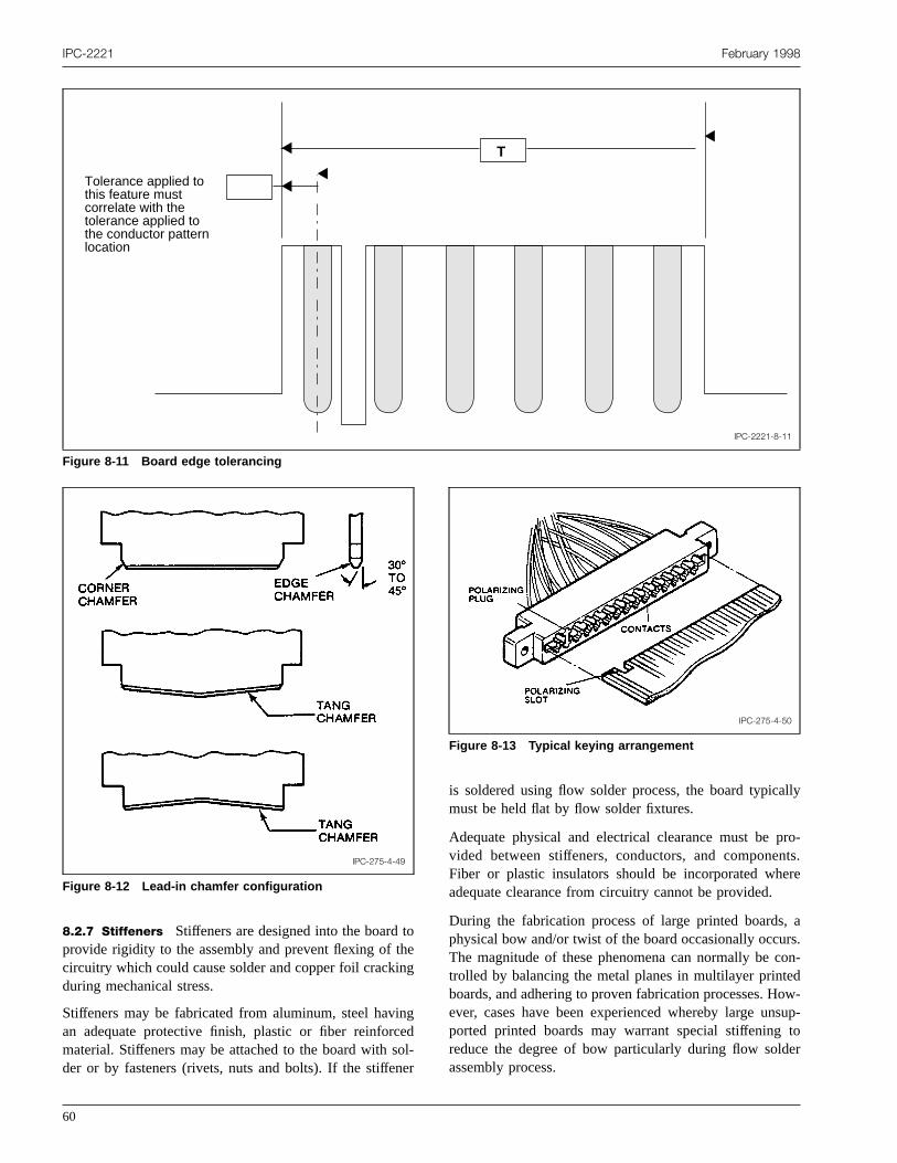
IPC-2221 February 1998
IPC-2221-8-11
Figure 8-11 Board edge tolerancing
▼ ▼
▼T
Tolerance applied to this feature must correlate with the tolerance applied to the conductor pattern location
▼
oeg
gdole
lly
ro-ts.re
as.n-dw-up-tor
8.2.7 Stiffeners Stiffeners are designed into the board tprovide rigidity to the assembly and prevent flexing of thcircuitry which could cause solder and copper foil crackinduring mechanical stress.
Stiffeners may be fabricated from aluminum, steel havinan adequate protective finish, plastic or fiber reinforcematerial. Stiffeners may be attached to the board with sder or by fasteners (rivets, nuts and bolts). If the stiffen
IPC-275-4-49
Figure 8-12 Lead-in chamfer configuration
60
-r
is soldered using flow solder process, the board typicamust be held flat by flow solder fixtures.
Adequate physical and electrical clearance must be pvided between stiffeners, conductors, and componenFiber or plastic insulators should be incorporated wheadequate clearance from circuitry cannot be provided.
During the fabrication process of large printed boards,physical bow and/or twist of the board occasionally occurThe magnitude of these phenomena can normally be cotrolled by balancing the metal planes in multilayer printeboards, and adhering to proven fabrication processes. Hoever, cases have been experienced whereby large unsported printed boards may warrant special stiffeningreduce the degree of bow particularly during flow soldeassembly process.
IPC-275-4-50
Figure 8-13 Typical keying arrangement

forjec
rd
)of
f-
ldpi-tedofja-
inbeur.w-
blec-ick-er
-tos,ts
po-as-
op-e
herd
ered55c-ureeter
orc-f itn-a
February 1998 IPC-2221
The following is to be used as a general design guideestablishing the mechanical characteristics of the substiffening member(s).
E = E1h3
I
Wo (a + 5)300Z
E = Young’s modulus of stiffener material (lb./inch2)I = Moment of inertia (lb. inch2)E1 = Flexural modulus of elasticity of the printed boa
base material (lb./inch2)h = Thickness of the printed board (inch)Wo = Initial offset of the printed board, due to bow (incha = Dimension of the printed board, in the direction
bow (inch)Z = Allowable offset of the printed board after the stif
ening member is added (inch)
IPC-275-4-46
Figure 8-14 Two-part connector
IPC-275-4-47
Figure 8-15 Edge-board adapter connector
t
Provision for the addition of stiffening member(s) shoube provided to otherwise unsupported printed boards (tycally larger than 230 mm as measured along the prinboard connector side). To allow for proper engagementthe printed board connector, the stiffener should be adcent to the printed board connector(s).
8.2.8 Lands for Flattened Round Leads Flattened round(coined) leadsshall have a land which will provide theseating so that the heel and the terminal relationship isaccordance with Figure 8-16. Lead and land size shoulddesigned so that a minimum side overhang may occ(Class 3 product allows for a manufacturing process alloance of up to 1/4 of the lead diameter to overhang.)
A manufacturing allowance for toe overhang is acceptaprovided it does not violate the minimum designed condutor spacing. If flattened leads are used, the flattened thnessshall not be less than 40% of the original diamet(see J-STD-001).
8.2.9 Solder Terminals Single-/double-ended, or single/multi-sectioned turret solder terminals may be usedfacilitate the installation of components, jumper wireinput/output wiring, etc. The wires or leads of componenshall be soldered to the posts of the solder terminals.
Eyelets and solder terminals are to be considered comnents and specified on the assembly drawing or a subsembly drawing for board fabrication.
8.2.9.1 Terminal Mounting-Mechanical Solder termi-nals that are not connected to conductive patterns or cper planesshall be of the rolled flange configuration (seFigure 8-17A).
8.2.9.2 Terminal Mounting-Electrical For printedboards or printed board assemblies, solder terminalsshallbe of the flange configuration shown in Figure 8-17B. Tterminalshall be approximately perpendicular to the boasurface and may be free to rotate.
Flat body flangesshall be seated to the base material of thprinted board and not on ground planes or lands. Flaflangesshall be formed to an included angle between 3and 120 degrees andshall extend between 0.4 mm and 1.mm beyond the surface of the land provided minimal eletrical spacing requirements are maintained (see Fig8-17B) and the flare diameter does not exceed the diamof the land.
Terminals should only be mounted in unsupported holesin plated-through holes in Type 2 boards with a nonfuntional land on the component side (see Figure 8-17B). Iis essential that a terminal be utilized for interfacial conection, on Type 3 through Type 6 (inclusive) boards,
61

IPC-2221 February 1998
IPC-001-025
Figure 8-16 Round or flattened (coined) lead joint description
IPC-275-4-51
Figure 8-17 Standoff terminal mounting, mm
d
e
hereof ar-aype-
dual hole configuration incorporating a supported platethrough holeshall be combined with the terminal holeinterconnected by a land on the solder side of the printboard (see Figure 8-18).
8.2.9.3 Attachment of Wires/Leads to Terminals Incases in which more than one wire is attached to a term
62
-
d
i-
nal, the largest diameter wire should be mounted to tbottom-most post for ease of rework and repair. No mothan three attachments should be made to each sectionturret of bifurcated terminal. As an exception, bus bar teminals (see sectional standards for more information) mhold more than three wires or leads per section when scifically designed to hold more.
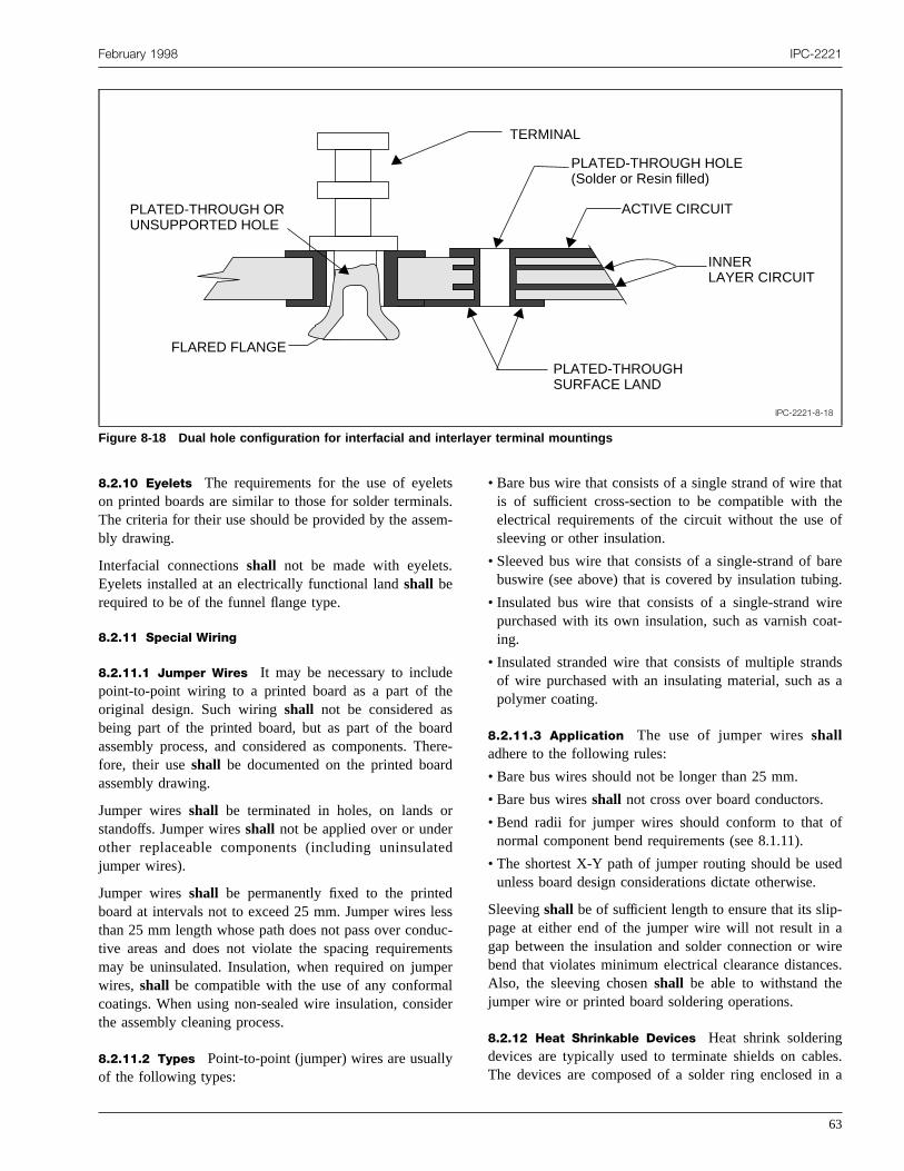
February 1998 IPC-2221
IPC-2221-8-18
Figure 8-18 Dual hole configuration for interfacial and interlayer terminal mountings
PLATED-THROUGH SURFACE LAND
▼ ▼
FLARED FLANGE
TERMINAL
PLATED-THROUGH OR UNSUPPORTED HOLE
PLATED-THROUGH HOLE (Solder or Resin filled)
▼
▼
ACTIVE CIRCUIT
INNER LAYER CIRCUIT
▼
▼▼
▼
▼
tsalsm
.
ehesardherd
rrte
dlesduenpealide
y
ateof
areng.
ireat-
dsa
f
ed
-airees.
les.in a
8.2.10 Eyelets The requirements for the use of eyeleon printed boards are similar to those for solder terminThe criteria for their use should be provided by the assebly drawing.
Interfacial connectionsshall not be made with eyeletsEyelets installed at an electrically functional landshall berequired to be of the funnel flange type.
8.2.11 Special Wiring
8.2.11.1 Jumper Wires It may be necessary to includpoint-to-point wiring to a printed board as a part of toriginal design. Such wiringshall not be considered abeing part of the printed board, but as part of the boassembly process, and considered as components. Tfore, their useshall be documented on the printed boaassembly drawing.
Jumper wiresshall be terminated in holes, on lands ostandoffs. Jumper wiresshall not be applied over or undeother replaceable components (including uninsulajumper wires).
Jumper wiresshall be permanently fixed to the printeboard at intervals not to exceed 25 mm. Jumper wiresthan 25 mm length whose path does not pass over contive areas and does not violate the spacing requiremmay be uninsulated. Insulation, when required on jumwires, shall be compatible with the use of any conformcoatings. When using non-sealed wire insulation, consthe assembly cleaning process.
8.2.11.2 Types Point-to-point (jumper) wires are usuallof the following types:
.-
re-
d
sc-tsr
r
• Bare bus wire that consists of a single strand of wire this of sufficient cross-section to be compatible with thelectrical requirements of the circuit without the usesleeving or other insulation.
• Sleeved bus wire that consists of a single-strand of bbuswire (see above) that is covered by insulation tubi
• Insulated bus wire that consists of a single-strand wpurchased with its own insulation, such as varnish coing.
• Insulated stranded wire that consists of multiple stranof wire purchased with an insulating material, such aspolymer coating.
8.2.11.3 Application The use of jumper wiresshalladhere to the following rules:
• Bare bus wires should not be longer than 25 mm.
• Bare bus wiresshall not cross over board conductors.
• Bend radii for jumper wires should conform to that onormal component bend requirements (see 8.1.11).
• The shortest X-Y path of jumper routing should be usunless board design considerations dictate otherwise.
Sleevingshall be of sufficient length to ensure that its slippage at either end of the jumper wire will not result ingap between the insulation and solder connection or wbend that violates minimum electrical clearance distancAlso, the sleeving chosenshall be able to withstand thejumper wire or printed board soldering operations.
8.2.12 Heat Shrinkable Devices Heat shrink solderingdevices are typically used to terminate shields on cabThe devices are composed of a solder ring enclosed
63
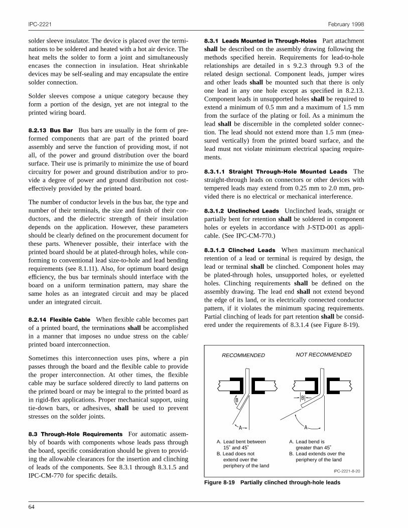
rmThslyblnti
thhe
e-ardnotrdardo-st
ann-ontet fothoningigthethece
rt
abl
pividleoaingt
-ugvidingan
heoletheiresly.13.
mec-ea-there-
ithro-
rtpli-
lheytted
torts.
9).
IPC-2221 February 1998
solder sleeve insulator. The device is placed over the tenations to be soldered and heated with a hot air device.heat melts the solder to form a joint and simultaneouencases the connection in insulation. Heat shrinkadevices may be self-sealing and may encapsulate the esolder connection.
Solder sleeves compose a unique category becauseform a portion of the design, yet are not integral to tprinted wiring board.
8.2.13 Bus Bar Bus bars are usually in the form of prformed components that are part of the printed boassembly and serve the function of providing most, ifall, of the power and ground distribution over the boasurface. Their use is primarily to minimize the use of bocircuitry for power and ground distribution and/or to prvide a degree of power and ground distribution not coeffectively provided by the printed board.
The number of conductor levels in the bus bar, the typenumber of their terminals, the size and finish of their coductors, and the dielectric strength of their insulatidepends on the application. However, these parameshould be clearly defined on the procurement documenthese parts. Whenever possible, their interface withprinted board should be at plated-through holes, while cforming to conventional lead size-to-hole and lead bendrequirements (see 8.1.11). Also, for optimum board desefficiency, the bus bar terminals should interface withboard on a uniform termination pattern, may sharesame holes as an integrated circuit and may be plaunder an integrated circuit.
8.2.14 Flexible Cable When flexible cable becomes paof a printed board, the terminationsshall be accomplishedin a manner that imposes no undue stress on the cprinted board interconnection.
Sometimes this interconnection uses pins, where apasses through the board and the flexible cable to prothe proper interconnection. At other times, the flexibcable may be surface soldered directly to land patternsthe printed board or may be integral to the printed boardin rigid-flex applications. Proper mechanical support, ustie-down bars, or adhesives,shall be used to prevenstresses on the solder joints.
8.3 Through-Hole Requirements For automatic assembly of boards with components whose leads pass throthe board, specific consideration should be given to proing the allowable clearances for the insertion and clinchof leads of the components. See 8.3.1 through 8.3.1.5IPC-CM-770 for specific details.
64
i-e
ere
ey
-
d
rsre-
n
d
e/
ne
ns
h-
d
8.3.1 Leads Mounted in Through-Holes Part attachmentshall be described on the assembly drawing following tmethods specified herein. Requirements for lead-to-hrelationships are detailed in s 9.2.3 through 9.3 ofrelated design sectional. Component leads, jumper wand other leadsshall be mounted such that there is onone lead in any one hole except as specified in 8.2Component leads in unsupported holesshall be required toextend a minimum of 0.5 mm and a maximum of 1.5 mfrom the surface of the plating or foil. As a minimum thlead shall be discernible in the completed solder connetion. The lead should not extend more than 1.5 mm (msured vertically) from the printed board surface, andlead must not violate minimum electrical spacing requiments.
8.3.1.1 Straight Through-Hole Mounted Leads Thestraight-through leads on connectors or other devices wtempered leads may extend from 0.25 mm to 2.0 mm, pvided there is no electrical or mechanical interference.
8.3.1.2 Unclinched Leads Unclinched leads, straight opartially bent for retentionshall be soldered in componenholes or eyelets in accordance with J-STD-001 as apcable. (See IPC-CM-770.)
8.3.1.3 Clinched Leads When maximum mechanicaretention of a lead or terminal is required by design, tlead or terminalshall be clinched. Component holes mabe plated-through holes, unsupported holes, or eyeleholes. Clinching requirementsshall be defined on theassembly drawing. The lead endshall not extend beyondthe edge of its land, or its electrically connected conducpattern, if it violates the minimum spacing requiremenPartial clinching of leads for part retentionshall be consid-ered under the requirements of 8.3.1.4 (see Figure 8-1
IPC-2221-8-20
Figure 8-19 Partially clinched through-hole leads
B
A
B
A
RECOMMENDED NOT RECOMMENDED
A.Lead bent between 15˚ and 45˚ B.Lead does not extend over the periphery of the land
A.Lead bend is greater than 45˚ B.Lead extends over the periphery of the land
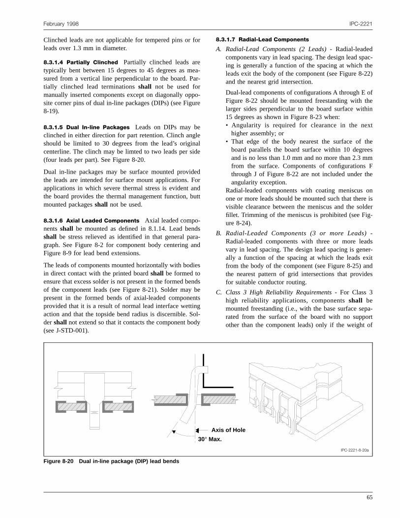
fo
ear
or
leade
eFonu
dran
e
nbngod
pac-he22)
ofthehin
xt
theeesmmFhe
onre islderg-
)adsner-xitnddes
pa-ortof
February 1998 IPC-2221
Clinched leads are not applicable for tempered pins orleads over 1.3 mm in diameter.
8.3.1.4 Partially Clinched Partially clinched leads aretypically bent between 15 degrees to 45 degrees as msured from a vertical line perpendicular to the board. Ptially clinched lead terminationsshall not be used formanually inserted components except on diagonally oppsite corner pins of dual in-line packages (DIPs) (see Figu8-19).
8.3.1.5 Dual In-line Packages Leads on DIPs may beclinched in either direction for part retention. Clinch angshould be limited to 30 degrees from the lead’s origincenterline. The clinch may be limted to two leads per si(four leads per part). See Figure 8-20.
Dual in-line packages may be surface mounted providthe leads are intended for surface mount applications.applications in which severe thermal stress is evident athe board provides the thermal management function, bmounted packagesshall not be used.
8.3.1.6 Axial Leaded Components Axial leaded compo-nentsshall be mounted as defined in 8.1.14. Lead benshall be stress relieved as identified in that general pagraph. See Figure 8-2 for component body centering aFigure 8-9 for lead bend extensions.
The leads of components mounted horizontally with bodiin direct contact with the printed boardshall be formed toensure that excess solder is not present in the formed beof the component leads (see Figure 8-21). Solder maypresent in the formed bends of axial-leaded componeprovided that it is a result of normal lead interface wettinaction and that the topside bend radius is discernible. Sdershall not extend so that it contacts the component bo(see J-STD-001).
r
a--
-e
l
drdtt
s-d
s
dsets
l-y
8.3.1.7 Radial-Lead Components
A. Radial-Lead Components (2 Leads)- Radial-leadedcomponents vary in lead spacing. The design lead sing is generally a function of the spacing at which tleads exit the body of the component (see Figure 8-and the nearest grid intersection.
Dual-lead components of configurations A through EFigure 8-22 should be mounted freestanding withlarger sides perpendicular to the board surface wit15 degrees as shown in Figure 8-23 when:• Angularity is required for clearance in the nehigher assembly; or
• That edge of the body nearest the surface ofboard parallels the board surface within 10 degrand is no less than 1.0 mm and no more than 2.3from the surface. Components of configurationsthrough J of Figure 8-22 are not included under tangularity exception.
Radial-leaded components with coating meniscusone or more leads should be mounted such that thevisible clearance between the meniscus and the sofillet. Trimming of the meniscus is prohibited (see Fiure 8-24).
B. Radial-Leaded Components (3 or more Leads-Radial-leaded components with three or more levary in lead spacing. The design lead spacing is geally a function of the spacing at which the leads efrom the body of the component (see Figure 8-25) athe nearest pattern of grid intersections that provifor suitable conductor routing.
C. Class 3 High Reliability Requirements- For Class 3high reliability applications, componentsshall bemounted freestanding (i.e., with the base surface serated from the surface of the board with no suppother than the component leads) only if the weight
IPC-2221-8-20a
Figure 8-20 Dual in-line package (DIP) lead bends
▼
▼
▼
30° Max.
Axis of Hole
65

IPC-2221 February 1998
IPC-2221-8-21
Figure 8-21 Solder in the lead bend radius
IPC I 00220
IIPC-275-4-15
Figure 8-22 Two-lead radial-leaded components
A B C D
Crystal Can
Device
Molded Box
Capacitor
Wafer Capacitor
Diode
E
Pocketbook Capacitor
F
Molded Box
Resistor
G
Test Point
H
Orangedrop Capacitor
J
Miniature Choke
mino
h
-g
ntedvethepo-
ntntststhee-26.
e.27ads
the component is 3.5 gm per lead or less. When coponents have an integral seating plane, the seatplane may be in contact with the board. When compnents are mounted freestanding, the spacing betwethe surface of the component and the surface of tboardshall be a minimum of 0.25 mm and a maximumof 2.5 mm.
IPC-2221-8-24
Figure 8-23 Radial two-lead component mounting, mm
▼▼
▼▼
0.4 mm Min. 0.4 mm Min.
▼▼
2.0 mm Max
▼▼ 15° Max
66
-g-ene
In no instanceshall non-parallelism result in nonconformance with the minimum or maximum spacinlimit.
8.3.1.8 Perpendicular (Vertical) Mounting Axial-leadedcomponents weighing less than 14 grams may be mouon the assembly using vertical mounting criteria that hathe major axis of the component body perpendicular toboard surface. The space between the end of the comnent body (or lead weld) and the boardshall be a minimumof 0.25 mm. Height restriction for general componemounting normally pertains to axial-leaded componemounted vertically. In general, the profile of componenshould be kept as low as possible to the surface ofboard. A maximum allowable vertical height from thboard mounting surface should be 15 mm, see Figure 8
8.3.1.9 Flat-Packs Flat-pack components normally havflat ribbon leads that exit from the component body on 1mm lead centers (see Figure 8-27). Forming of the le
IPC-275-4-17
Figure 8-24 Meniscus clearance, mm
▼ ▼
Meniscus
0.25 min.
IPC-2221-8-25
Figure 8-25 ‘‘TO’’ can radial-leaded component, mm
• ••
••
•••••••
••
• • • •
30˚ TYP
5.84mm DIA Bolt Circle
SEA ANG PLANE
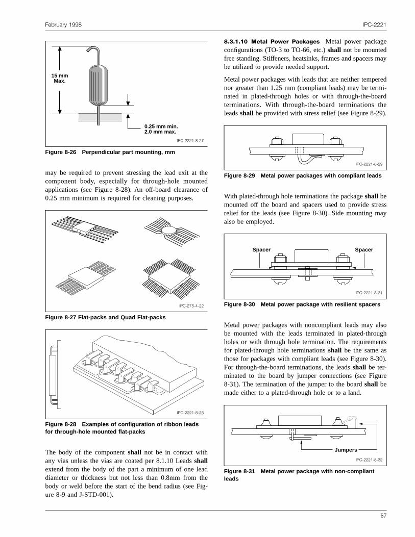
thdo
dheig-
may
eredmi-ardhe9).
tressay
lsoghnts
30).
ure
February 1998 IPC-2221
may be required to prevent stressing the lead exit atcomponent body, especially for through-hole mounteapplications (see Figure 8-28). An off-board clearance0.25 mm minimum is required for cleaning purposes.
The body of the componentshall not be in contact withany vias unless the vias are coated per 8.1.10 Leadsshallextend from the body of the part a minimum of one leadiameter or thickness but not less than 0.8mm from tbody or weld before the start of the bend radius (see Fure 8-9 and J-STD-001).
IPC-2221-8-27
Figure 8-26 Perpendicular part mounting, mm
▼
▼ ▼
▼
15 mm Max.
0.25 mm min. 2.0 mm max.
IPC-275-4-22
Figure 8-27 Flat-packs and Quad Flat-packs
IPC-2221-8-28
Figure 8-28 Examples of configuration of ribbon leadsfor through-hole mounted flat-packs
e
f
8.3.1.10 Metal Power Packages Metal power packageconfigurations (TO-3 to TO-66, etc.)shall not be mountedfree standing. Stiffeners, heatsinks, frames and spacersbe utilized to provide needed support.
Metal power packages with leads that are neither tempnor greater than 1.25 mm (compliant leads) may be ternated in plated-through holes or with through-the-boterminations. With through-the-board terminations tleadsshall be provided with stress relief (see Figure 8-2
With plated-through hole terminations the packageshall bemounted off the board and spacers used to provide srelief for the leads (see Figure 8-30). Side mounting malso be employed.
Metal power packages with noncompliant leads may abe mounted with the leads terminated in plated-throuholes or with through hole termination. The requiremefor plated-through hole terminationsshall be the same asthose for packages with compliant leads (see Figure 8-For through-the-board terminations, the leadsshall be ter-minated to the board by jumper connections (see Fig8-31). The termination of the jumper to the boardshall bemade either to a plated-through hole or to a land.
IPC-2221-8-29
Figure 8-29 Metal power packages with compliant leads
IPC-2221-8-31
Figure 8-30 Metal power package with resilient spacers
SpacerSpacer
IPC-2221-8-32
Figure 8-31 Metal power package with non-compliantleads
Jumpers
67

ersm-de
ghnetasilteddres
ntsce/ut-
nd-n-nt
75n.ithftheorbethrerd
as-hato1)
ntshe-o-meta-hreuld
heedmc-
eaedr-
e
-ya-
thp
e
eer--
re
re
ce
lylto
ressr
IPC-2221 February 1998
Care must be exercised when the mounting utilizes spacto ensure that any electrical connection between the coponent case and the board circuitry remains constant unall operating conditions.
Whenever the terminations are made in plated-throuholes, the mountingshall ensure that the connections cabe cleaned between the component and the board. Mpower packages, the standoffs, heatsink frames, and reient spacers on which metal power packages are mounshall be of configurations which do not block platethrough-holes, preclude excessive stresses (provide strelief), and facilitate cleaning.
8.4 Standard Surface Mount Requirements Automaticassembly considerations for surface mounted componeare driven by pick-and-place machines used to plaposition chip components, discrete chip carriers, small oline packages, and flat packs. Printed board designsshallmaintain appropriate clearances for the automatic pick-aplace equipment to position the parts in their proper orietation and allow sufficient clearances for the placemeheads. (See IPC-SM-780).
Typically, fine pitch devices could be between 250 and 7mm2 case size for automatic placement without visioGenerally, the largest component that can be placed wvision alignment is 1300 mm2, measured to the outside othe leads. Large packages exaggerate the effects of themal mismatch between the component and substrate. Nmally, the minimum size leadless component that canplaced with automatic equipment is 1.5 mm nominal lengby 0.75 mm nominal width. Smaller components requihigh placement accuracy. Vacuum pickup with standaequipment is also difficult.
Avoid extremely small passive components. Leadless psive components should have an aspect ratio greater tone and less than three. High aspect ratio parts tendfracture during soldering. Square devices (aspect ratio =are difficult to orient.
Smaller components are easier to solder, but footprimust be large enough to permit reliable placement of adsive without smearing onto the conductor. Avoid compnents which require mounting land spacings (on the sacomponent) closer than 0.75 mm, due to process limitions on applying (chip bonding or thermal adhesive). Higprofile SMT components (higher than 2.5 mm) interfewith wave solder flow to adjacent components, and shobe avoided.
Special orientation symbols should be incorporated into tdesign to allow for ease of inspection of the assemblsurface mounted part. Techniques may include special sybols, or special land configurations to identify such charateristics as pin 1 of an integrated circuit package.
68
r
l-
s
r--
n
-
8.4.1 Surface-Mounted Leaded Components Therequirements and consideration of 8.1.14 apply to thsurface-mounting of leaded components. Lead forming ismajor design consideration. Custom lead forms should bdescribed on the assembly drawing to provide for leastress relief to ensure fit to the land pattern to allow undebody clearance for cleaning, and to provide anydesigned-in provisions for thermal transfer (see Figur8-32). (See IPC-SM-782.)
Axial leaded components may be surface mounted provided the leads are coined (see Figure 8-33). However, themay never be surface mounted in a perpendicular orienttion (see Figure 8-26).
8.4.2 Flat-pack Components Flat-pack components nor-mally have flat ribbon leads that exit from the componenbody on 1.27 mm lead centers (see Figure 8-34). Althougthey generally have from 14 to 16 leads, flat-packs with uto 50 leads are available.
When planar mounted flat-packs require lead forming, thleadsshall be configured as shown in Figure 8-34. Non-insulated parts mounted over exposed circuitryshall havetheir leads formed to provide a minimum of 0.25 mmbetween the bottom of the component body and thexposed circuitry. The maximum clearance between thbottom of the leaded component body and the printed wiing surface should be 2.0 mm. Parts insulated from circuitry or over surfaces without exposed circuitry may bemounted flush. If the component requires thermal transfeto the board, special consideration for cleaning should bgiven.
8.4.3 Ribbon Lead Termination Flat-wire ribbon leadsmay be attached to lands on the printed board (see Figu8-35). Connectionsshall be made by soldering or wirebonding only.
8.4.4 Round Lead Termination In some instances, com-ponents with round leads may be attached to the surfalands without first passing through a hole. The landshallbe designed with the proper shape and spacing to compwith proper soldering techniques. Components with axialeads of round cross-section may be coined or flattenedprovide positive mounting (see Figure 8-33).
8.4.5 Component Lead Sockets Component lead sock-ets may be allowed for Class 3 high reliability require-ments when engineering analysis proves acceptable. Cashould be taken in specifying the use of non-noble platingor finishes on either sockets or the component leadbecause of the possibility of producing inherent heat oopen circuits due to fret corrosion during vibration or tem-perature cycling.
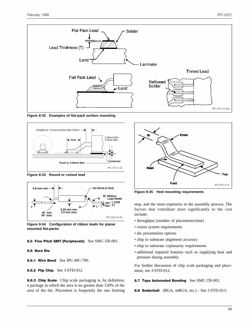
February 1998 IPC-2221
IPC-2221-8-32a
Figure 8-32 Examples of flat-pack surface mounting
,thg
Thest
nd
ce-
8.5 Fine Pitch SMT (Peripherals) See SMC-TR-001.
8.6 Bare Die
8.6.1 Wire Bond See IPC-MC-790.
8.6.2 Flip Chip See J-STD-012.
8.6.3 Chip Scale Chip scale packaging is, by definitiona package in which the area is no greater than 120% ofarea of the die. Placement is frequently the rate limitin
IPC-275-4-32
Figure 8-33 Round or coined lead
▼▼
Flush to 0.65mm Max
▼
Foot
▼
▼
▼
▼
▼
Straight for 1 D but not less than 0.8mm
0.25mm Min. 2.0mm Max.
Conductor
▼
IPC-2221-8-35
Figure 8-34 Configuration of ribbon leads for planarmounted flat-packs
0.8 mm
min.
▼
▼
▼
▼
45° min. 90° max.
0.25 mm min. 2.0 mm max.
▼
R
▼ R▼
▼ ▼L
No Bend at Seal
W: Ribbon Lead WidthL : 1 1/2WMINR : 1TMIN
▼ ▼
▼▼
T
e
step, and the most expensive in the assembly process.factors that contribute most significantly to the coinclude:
• throughput (number of placements/time)
• vision system requirements
• die presentation options
• chip to substrate alignment accuracy
• chip to substrate coplanarity requirements
• additional required features such as supplying heat apressure during assembly
For further discussion of chip scale packaging and plament, see J-STD-012.
8.7 Tape Automated Bonding See SMC-TR-001.
8.8 Solderball (BGA, mBGA, etc.) - See J-STD-013.
IPC-275-4-31
Figure 8-35 Heel mounting requirements
69
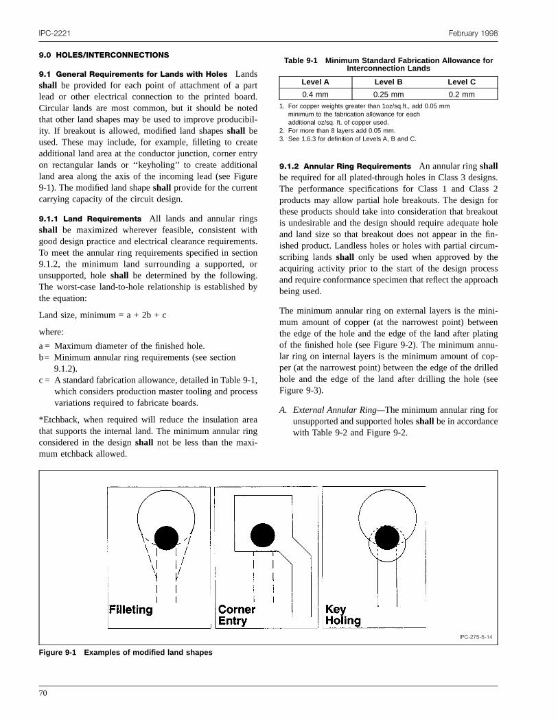
rtrdedbi
tetrlur
thntioor
b
1s
ang
ns.2
oroutolefin--
esach
i-eningu--ledee
IPC-2221 February 1998
9.0 HOLES/INTERCONNECTIONS
9.1 General Requirements for Lands with Holes Landsshall be provided for each point of attachment of a palead or other electrical connection to the printed boaCircular lands are most common, but it should be notthat other land shapes may be used to improve produciity. If breakout is allowed, modified land shapesshall beused. These may include, for example, filleting to creaadditional land area at the conductor junction, corner enon rectangular lands or ‘‘keyholing’’ to create additionaland area along the axis of the incoming lead (see Fig9-1). The modified land shapeshall provide for the currentcarrying capacity of the circuit design.
9.1.1 Land Requirements All lands and annular ringsshall be maximized wherever feasible, consistent wigood design practice and electrical clearance requiremeTo meet the annular ring requirements specified in sect9.1.2, the minimum land surrounding a supported,unsupported, holeshall be determined by the following.The worst-case land-to-hole relationship is establishedthe equation:
Land size, minimum = a + 2b + c
where:
a = Maximum diameter of the finished hole.b= Minimum annular ring requirements (see section
9.1.2).c = A standard fabrication allowance, detailed in Table 9-
which considers production master tooling and procevariations required to fabricate boards.
*Etchback, when required will reduce the insulation arethat supports the internal land. The minimum annular riconsidered in the designshall not be less than the maxi-mum etchback allowed.
70
.
l-
y
e
s.n
y
,s
9.1.2 Annular Ring Requirements An annular ringshallbe required for all plated-through holes in Class 3 desigThe performance specifications for Class 1 and Classproducts may allow partial hole breakouts. The design fthese products should take into consideration that breakis undesirable and the design should require adequate hand land size so that breakout does not appear in theished product. Landless holes or holes with partial circumscribing landsshall only be used when approved by thacquiring activity prior to the start of the design procesand require conformance specimen that reflect the approbeing used.
The minimum annular ring on external layers is the minmum amount of copper (at the narrowest point) betwethe edge of the hole and the edge of the land after platof the finished hole (see Figure 9-2). The minimum annlar ring on internal layers is the minimum amount of copper (at the narrowest point) between the edge of the drilhole and the edge of the land after drilling the hole (sFigure 9-3).
A. External Annular Ring—The minimum annular ring forunsupported and supported holesshall be in accordancewith Table 9-2 and Figure 9-2.
Table 9-1 Minimum Standard Fabrication Allowance forInterconnection Lands
Level A Level B Level C
0.4 mm 0.25 mm 0.2 mm1. For copper weights greater than 1oz/sq.ft., add 0.05 mm
minimum to the fabrication allowance for eachadditional oz/sq. ft. of copper used.
2. For more than 8 layers add 0.05 mm.3. See 1.6.3 for definition of Levels A, B and C.
IPC-275-5-14
Figure 9-1 Examples of modified land shapes

ch-rt-m
r-es,ingl-
enec-
in
ideadro-toressee
tsjorvs.
ionion.osi-n-rity.sic
eried
ntsedal
February 1998 IPC-2221
B. Internal Annular Ring—The minimum annular ring forinternal lands on multilayer and metal core boardsshallbe in accordance with Table 9-2 and Figure 9-3. Etback, when required, will reduce the insulation suppoing the annular ring of internal lands. The minimuannular ring considered in the designshall be not lessthan the maximum etchback allowed.
IPC-275-5-15
Figure 9-2 External annular ring
▼
Plated- Through Hole
▼▼
▼
Min. Annular Ring
Land
▼
▼
IPC-275-5-16
Figure 9-3 Internal annular ring
Hole Plating
▼
▼▼ Minimum Annular Ring
▼▼ Minimum Annular Ring
Table 9-2 Annular Rings (Minimum)
Annular Ring Class 1, 2, and 3
Internal Supported 0.03 mm
External Supported 0.05 mm
External Unsupported 0.15 mm
9.1.3 Thermal Relief in Conductor Planes Thermalrelief is only required for holes that are subject to soldeing in large conductor areas (ground planes, voltage planthermal planes, etc.). Relief is required to reduce solderdwell time by providing thermal resistance during the sodering process.
These type connectionsshall be relieved in a manner simi-lar to that shown in Figure 9-4. The relationship betwethe hole size, land and web area is critical. See the stional standards for more detailed information.
9.1.4 Lands for Flattened Round Leads Flattened round(coined) leadsshall have a land which will provide theseating so that the heel and the terminal relationship isaccordance with Figure 8-33.
Lead and land size should be designed to minimize soverhang. (Class 3 product allows up to 1/4 of the lediameter to overhang.) Toe overhang is acceptable pvided it does not violate the minimum designed conducspacing. If flattened leads are used, the flattened thicknshall not be less than 40% of the original diameter (sJ-STD-001).
9.2 Holes
9.2.1 Location All holes and profilesshall be dimen-sioned in accordance with 5.4.
Note: The lead patterns of the majority of the componento be mounted on a printed board should be the mainfluence on choice of measurement system (metricinches).
9.2.2 Hole Location Tolerances Table 9-3, based onglass/epoxy materials, shows the values for hole locattolerances that are to be applied to the basic hole positAll tolerances are expressed as diameter about true ption. These tolerances only take into account drill positioing and drill drift. The basic hole position may be furtheaffected by material thickness, type and the copper densThe effect is usually a reduction (shrinkage) between bahole positions.
9.2.3 Quantity A separate component holeshall be pro-vided for each lead, terminal of a part, or end of a jumpwire that is to be through-hole mounted, except as specifin 8.2.11.
9.2.4 Spacing of Adjacent Holes The spacing of unsup-ported or plated-through holes (or both)shall be such thatthe lands surrounding the holes meet spacing requiremeof the 6.3. Consideration should be given to the printboard material structural requirements, with the residulaminate material being no less than 0.5 mm.
71

IPC-2221 February 1998
IPC-275-5-17
Figure 9-4 Typical thermal relief in planes
Land Before Drilling
Land After Drilling
Wide Straps Narrow Straps
Web Width
▼▼
nhe
g
,nn
mri
ch
ser
dsee
oro
ri-sne-msseri-r
rhe
y-ohenott-eis
es.
9.2.5 Hole Pattern Variation When a modular gridincrement is selected, see 5.4.2, parts whose leads emain a pattern that varies from the grid intersections of tmodular dimensioning system of the printed board,shallbe mounted on the printed board with one of the followinhole patterns.
A hole pattern where the hole, for at least one part leadlocated at a grid intersection of the modular dimensionisystem, and the other holes of the pattern are dimensiofrom that grid location.
A hole pattern where the center of the pattern is locateda grid intersection of the modular dimensioning systeand all holes of the pattern are dimensioned from that glocation.
9.2.6 Aspect Ratio The aspect ratio of plated-throughholes plays an important part in the ability of the manufaturer to provide sufficient plating within the plated-throughole.
9.2.6.1 Plated-Through Hole Tolerances When usingthe basic dimensioning system, plated-through holes uto attach component leads or pins to the printed boashould be expressed in terms of MMC and LMC limits.
9.2.7 Blind and Buried Vias Plated-through holes con-necting two or more conductive layers of multilayer printeboard, but not extending fully through all layers of the bamaterial comprising the board, are called blind and burivias.
Table 9-3 Minimum Hole Location Tolerance, dtp
Level A Level B Level C
0.25 mm 0.2 mm 0.15 mm
72
ate
isged
at,d
-
dd
d
9.2.7.1 Blind Vias Blind via plated-through holes extendfrom the surface and connect the surface layer with onemore internal layers. The blind via can be produced by twmethods: (1) After multilayer lamination by drilling a holefrom the surface to the internal layers desired and electcally interconnecting them by plating the blind via holeduring the plating process; (2) Before multilayer laminatioby drilling the blind via holes from the surface layers to thfirst or last buried layers and plating them through, imaging and etching the internal sides, and then laminating thein the multilayer bonding process. For the second proceif an interconnection is desired between the surface layand more than one internal layer, sequential etching, lamnating, drilling and plating-through of these layers togethebefore final multilayer lamination is required. Blind viaholes should be filled or plugged with a polymer or solderesist to prevent solder form entering them as solder in tsmall holes decreases reliability.
9.2.7.2 Buried Vias Buried via plated-through holes donot extend to the surface but interconnect only internal laers. Most commonly the interconnection is between twadjacent internal layers. These are produced by drilling tthin laminate material, plating the holes through and theetching the internal layer pattern on the layers prior tmultilayer lamination. Buried vias between non-adjacenlayers requires sequential etching of inside layers, laminaing them together, drilling the laminated panel, plating thholes through, etching external sides and laminating thpanel into the final multilayer panel.
9.2.7.3 Hole Size of Blind and Buried Vias Small holesare usually used for either blind or buried vias and may bproduced mechanically, by laser or by plasma techniqueThe minimum drilled hole size for buried vias is shown in
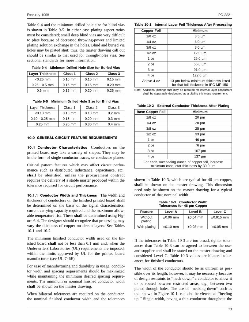
sioulteiaoue
bs
r-tch
icw
ale
-ed
ucee-th
toe
r,oncal
er-userder-
s-useittwoasnge
February 1998 IPC-2221
Table 9-4 and the minimum drilled hole size for blind viais shown in Table 9-5. In either case plating aspect ratmust be considered; small deep blind vias are very difficto plate because of decreased throwing-power and limiplating solution exchange in the holes. Blind and buried vholes may be plated shut; thus, the master drawing callshould be similar to that used for through-holes vias. Ssectional standards for more information.
10.0 GENERAL CIRCUIT FEATURE REQUIREMENTS
10.1 Conductor Characteristics Conductors on theprinted board may take a variety of shapes. They mayin the form of single conductor traces, or conductor plane
Critical pattern features which may affect circuit perfomance such as distributed inductance, capacitance, eshall be identified, unless the procurement contrarequires the delivery of a stable master produced within ttolerance required for circuit performance.
10.1.1 Conductor Width and Thickness The width andthickness of conductors on the finished printed boardshallbe determined on the basis of the signal characteristcurrent carrying capacity required and the maximum alloable temperature rise. Theseshall be determined using Fig-ure 6-4. The designer should recognize that processing mvary the thickness of copper on circuit layers. See Tab10-1 and 10-2
The minimum finished conductor width used on the finished boardshall not be less than 0.1 mm and, when thUnderwriters Laboratories (UL) requirements are imposewithin the limits approved by UL for the printed boardmanufacturer (see UL 746E).
For ease of manufacturing and durability in usage, condtor width and spacing requirements should be maximizwhile maintaining the minimum desired spacing requirments. The minimum or nominal finished conductor widshall be shown on the master drawing.
When bilateral tolerances are required on the conducthe nominal finished conductor width and the toleranc
Table 9-4 Minimum Drilled Hole Size for Buried Vias
Layer Thickness Class 1 Class 2 Class 3
<0.25 mm 0.10 mm 0.10 mm 0.15 mm
0.25 - 0.5 mm 0.15 mm 0.15 mm 0.20 mm
0.5 mm 0.15 mm 0.20 mm 0.25 mm
Table 9-5 Minimum Drilled Hole Size for Blind Vias
Layer Thickness Class 1 Class 2 Class 3
<0.10 mm 0.10 mm 0.10 mm 0.2 mm
0.10 - 0.25 mm 0.15 mm 0.20 mm 0.3 mm
0.25 mm 0.20 mm 0.30 mm 0.4 mm
std
te
e.
c.,te
s,-
ys
,
-d
r,s
shown in Table 10-3, which are typical for 46 µm coppeshall be shown on the master drawing. This dimensineed only be shown on the master drawing for a typiconductor of that nominal width.
If the tolerances in Table 10-3 are too broad, tighter tolances than Table 10-3 can be agreed to between theand supplier andshall be stated on the master drawing anconsidered Level C. Table 10-3 values are bilateral tolances for finished conductors.
The width of the conductor should be as uniform as posible over its length; however, it may be necessary becaof design restraints to ‘‘neck down’’ a conductor to allowto be routed between restricted areas, e.g., betweenplated-through holes. The use of ‘‘necking down’’ suchthat shown in Figure 10-1, can also be viewed as ‘‘beefiup.’’ Single width, having a thin conductor throughout th
Table 10-1 Internal Layer Foil Thickness After Processing
Copper Foil Minimum
1/8 oz 3.5 µm
1/4 oz 6.0 µm
3/8 oz 8.0 µm
1/2 oz 12.0 µm
1 oz 25.0 µm
2 oz 56.0 µm
3 oz 91.0 µm
4 oz 122.0 µm
Above 4 oz 13 µm below minimum thickness listedfor that foil thickness in IPC-MF-150
Note: Additional platings that may be required for internal layer conductorsshall be separately designated as a plating thickness requirement.
Table 10-2 External Conductor Thickness After Plating
Base Copper Foil Minimum
1/8 oz 20 µm
1/4 oz 20 µm
3/8 oz 25 µm
1/2 oz 33 µm
1 oz 46 µm
2 oz 76 µm
3 oz 107 µm
4 oz 137 µm
For each succeeding ounce of copper foil, increaseminimum conductor thickness by 30.0 µm
Table 10-3 Conductor WidthTolerances for 46 µm Copper
Feature Level A Level B Level C
Withoutplating
±0.06 mm ±0.04 mm ±0.015 mm
With plating ±0.10 mm ±0.08 mm ±0.05 mm
73
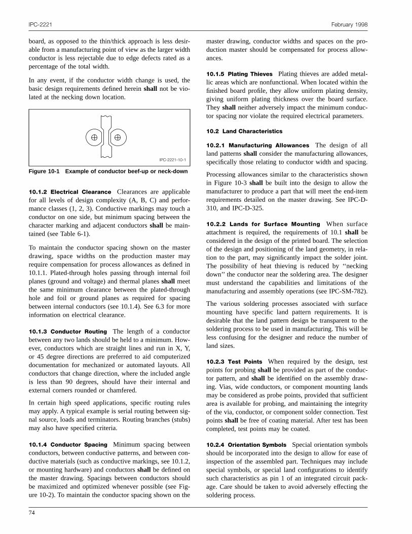
sithas
the
e-hth
teaydfo
ugingo
wY,zeAlgan
lesig-ub
co1.
ouigth
pro-low-
l-hey,e.c-s.
s,ng.
own
em-D-
tionla-t.gnerthe82).
faceistheber of
st--dsientityesten
ofudetifyck-the
IPC-2221 February 1998
board, as opposed to the thin/thick approach is less deable from a manufacturing point of view as the larger widconductor is less rejectable due to edge defects ratedpercentage of the total width.
In any event, if the conductor width change is used,basic design requirements defined hereinshall not be vio-lated at the necking down location.
10.1.2 Electrical Clearance Clearances are applicablfor all levels of design complexity (A, B, C) and performance classes (1, 2, 3). Conductive markings may toucconductor on one side, but minimum spacing betweencharacter marking and adjacent conductorsshall be main-tained (see Table 6-1).
To maintain the conductor spacing shown on the masdrawing, space widths on the production master mrequire compensation for process allowances as define10.1.1. Plated-through holes passing through internalplanes (ground and voltage) and thermal planesshall meetthe same minimum clearance between the plated-throhole and foil or ground planes as required for spacbetween internal conductors (see 10.1.4). See 6.3 for minformation on electrical clearance.
10.1.3 Conductor Routing The length of a conductorbetween any two lands should be held to a minimum. Hoever, conductors which are straight lines and run in X,or 45 degree directions are preferred to aid computeridocumentation for mechanized or automated layouts.conductors that change direction, where the included anis less than 90 degrees, should have their internalexternal corners rounded or chamfered.
In certain high speed applications, specific routing rumay apply. A typical example is serial routing between snal source, loads and terminators. Routing branches (stmay also have specified criteria.
10.1.4 Conductor Spacing Minimum spacing betweenconductors, between conductive patterns, and betweenductive materials (such as conductive markings, see 10.or mounting hardware) and conductorsshall be defined onthe master drawing. Spacings between conductors shbe maximized and optimized whenever possible (see Fure 10-2). To maintain the conductor spacing shown on
IPC-2221-10-1
Figure 10-1 Example of conductor beef-up or neck-down
74
r-
a
ae
r
inil
h
re
-
dlled
s)
n-2,
ld-e
master drawing, conductor widths and spaces on theduction master should be compensated for process alances.
10.1.5 Plating Thieves Plating thieves are added metalic areas which are nonfunctional. When located within tfinished board profile, they allow uniform plating densitgiving uniform plating thickness over the board surfacThey shall neither adversely impact the minimum condutor spacing nor violate the required electrical parameter
10.2 Land Characteristics
10.2.1 Manufacturing Allowances The design of allland patternsshall consider the manufacturing allowancespecifically those relating to conductor width and spaci
Processing allowances similar to the characteristics shin Figure 10-3shall be built into the design to allow themanufacturer to produce a part that will meet the end-itrequirements detailed on the master drawing. See IPC310, and IPC-D-325.
10.2.2 Lands for Surface Mounting When surfaceattachment is required, the requirements of 10.1shall beconsidered in the design of the printed board. The selecof the design and positioning of the land geometry, in retion to the part, may significantly impact the solder joinThe possibility of heat thieving is reduced by ‘‘neckindown’’ the conductor near the soldering area. The desigmust understand the capabilities and limitations ofmanufacturing and assembly operations (see IPC-SM-7
The various soldering processes associated with surmounting have specific land pattern requirements. Itdesirable that the land pattern design be transparent tosoldering process to be used in manufacturing. This willless confusing for the designer and reduce the numbeland sizes.
10.2.3 Test Points When required by the design, tepoints for probingshall be provided as part of the conductor pattern, andshall be identified on the assembly drawing. Vias, wide conductors, or component mounting lanmay be considered as probe points, provided that sufficarea is available for probing, and maintaining the integrof the via, conductor, or component solder connection. Tpointsshall be free of coating material. After test has becompleted, test points may be coated.
10.2.4 Orientation Symbols Special orientation symbolsshould be incorporated into the design to allow for easeinspection of the assembled part. Techniques may inclspecial symbols, or special land configurations to idensuch characteristics as pin 1 of an integrated circuit paage. Care should be taken to avoid adversely effectingsoldering process.
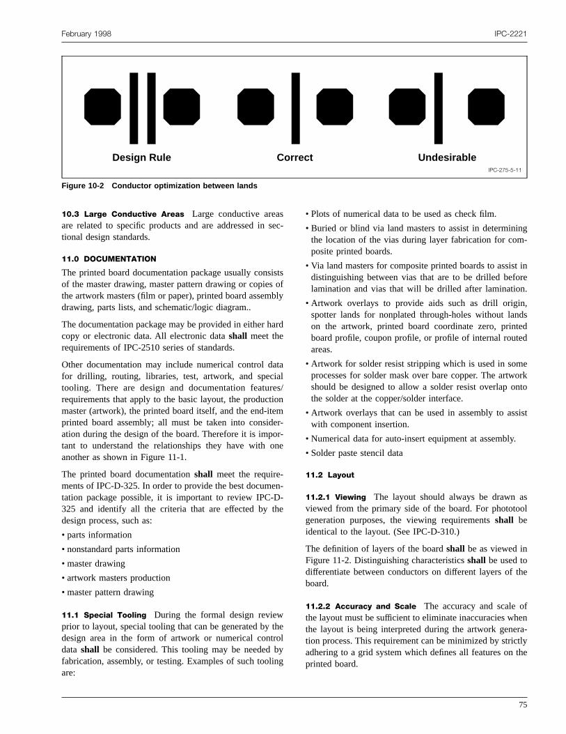
February 1998 IPC-2221
IPC-275-5-11
Figure 10-2 Conductor optimization between lands
Design Rule Correct Undesirable
se
isobl
ar
talesiomerr-n
n-e
holbyng
g-
t inre.
,dsedd
eorknto
ist
sol
he
fenra-tlythe
10.3 Large Conductive Areas Large conductive areasare related to specific products and are addressed intional design standards.
11.0 DOCUMENTATION
The printed board documentation package usually consof the master drawing, master pattern drawing or copiesthe artwork masters (film or paper), printed board assemdrawing, parts lists, and schematic/logic diagram..
The documentation package may be provided in either hcopy or electronic data. All electronic datashall meet therequirements of IPC-2510 series of standards.
Other documentation may include numerical control dafor drilling, routing, libraries, test, artwork, and speciatooling. There are design and documentation featurrequirements that apply to the basic layout, the productmaster (artwork), the printed board itself, and the end-iteprinted board assembly; all must be taken into considation during the design of the board. Therefore it is impotant to understand the relationships they have with oanother as shown in Figure 11-1.
The printed board documentationshall meet the require-ments of IPC-D-325. In order to provide the best documetation package possible, it is important to review IPC-D325 and identify all the criteria that are effected by thdesign process, such as:
• parts information
• nonstandard parts information
• master drawing
• artwork masters production
• master pattern drawing
11.1 Special Tooling During the formal design reviewprior to layout, special tooling that can be generated by tdesign area in the form of artwork or numerical contrdatashall be considered. This tooling may be neededfabrication, assembly, or testing. Examples of such tooliare:
c-
tsfy
d
/n
-
e
-
e
• Plots of numerical data to be used as check film.
• Buried or blind via land masters to assist in determininthe location of the vias during layer fabrication for composite printed boards.
• Via land masters for composite printed boards to assisdistinguishing between vias that are to be drilled befolamination and vias that will be drilled after lamination
• Artwork overlays to provide aids such as drill originspotter lands for nonplated through-holes without lanon the artwork, printed board coordinate zero, printboard profile, coupon profile, or profile of internal routeareas.
• Artwork for solder resist stripping which is used in somprocesses for solder mask over bare copper. The artwshould be designed to allow a solder resist overlap othe solder at the copper/solder interface.
• Artwork overlays that can be used in assembly to asswith component insertion.
• Numerical data for auto-insert equipment at assembly.
• Solder paste stencil data
11.2 Layout
11.2.1 Viewing The layout should always be drawn aviewed from the primary side of the board. For phototogeneration purposes, the viewing requirementsshall beidentical to the layout. (See IPC-D-310.)
The definition of layers of the boardshall be as viewed inFigure 11-2. Distinguishing characteristicsshall be used todifferentiate between conductors on different layers of tboard.
11.2.2 Accuracy and Scale The accuracy and scale othe layout must be sufficient to eliminate inaccuracies whthe layout is being interpreted during the artwork genetion process. This requirement can be minimized by stricadhering to a grid system which defines all features onprinted board.
75
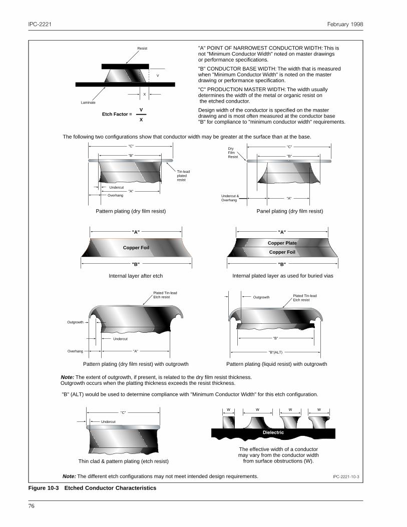
IPC-2221 February 1998
IPC-2221-10-3
Figure 10-3 Etched Conductor Characteristics
Resist
X
V
Laminate
Etch Factor =V
X
"C"
"B"
"A"Undercut
Overhang
Tin-lead plated resist
"C"
"B"
"A"Undercut & Overhang
Dry Film Resist
Copper Foil
"A"
"B"
Plated Tin-lead Etch resist
"A"
Undercut
Overhang
Outgrowth
Plated Tin-lead Etch resist
"B"
Outgrowth
"B"(ALT)
"C"
Undercut
Copper Plate
Copper Foil
"A"
"B"
"A" POINT OF NARROWEST CONDUCTOR WIDTH: This is not "Minimum Conductor Width" noted on master drawings or performance specifications.
Design width of the conductor is specified on the master drawing and is most often measured at the conductor base "B" for compliance to "minimum conductor width" requirements.
"C" PRODUCTION MASTER WIDTH: The width usually determines the width of the metal or organic resist on the etched conductor.
"B" CONDUCTOR BASE WIDTH: The width that is measured when "Minimum Conductor Width" is noted on the master drawing or performance specification.
The following two configurations show that conductor width may be greater at the surface than at the base.
Pattern plating (dry film resist)
Note: The extent of outgrowth, if present, is related to the dry film resist thickness. Outgrowth occurs when the platting thickness exceeds the resist thickness.
Internal layer after etch
Pattern plating (dry film resist) with outgrowth
Thin clad & pattern plating (etch resist)
The effective width of a conductor may vary from the conductor width
from surface obstructions (W).
Pattern plating (liquid resist) with outgrowth
Internal plated layer as used for buried vias
Panel plating (dry film resist)
"B" (ALT) would be used to determine compliance with "Minimum Conductor Width" for this etch configuration.
Note: The different etch configurations may not meet intended design requirements.
76
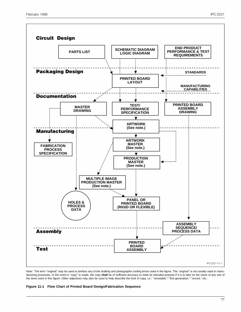
February 1998 IPC-2221
IPC-2221-11-1
Figure 11-1 Flow Chart of Printed Board Design/Fabrication Sequence
PARTS LISTSCHEMATIC DIAGRAM
LOGIC DIAGRAMEND PRODUCT
PERFORMANCE & TEST REQUIREMENTS
MASTER DRAWING
TEST/ PERFORMANCE SPECIFICATION
PRINTED BOARD ASSEMBLY DRAWING
ARTWORK MASTER
(See note.)
PRODUCTION MASTER
(See note.)
MULTIPLE IMAGE PRODUCTION MASTER
(See note.)
PANEL OR PRINTED BOARD
(RIGID OR FLEXIBLE)HOLES & PROCESS
DATA
ARTWORK (See note.)
ASSEMBLY SEQUENCE/
PROCESS DATA
PRINTED BOARD
ASSEMBLY
STANDARDS
MANUFACTURING CAPABILITIES
Circuit Design
Packaging Design
Documentation
Manufacturing
Assembly
Test
FABRICATION PROCESS
SPECIFICATION
PRINTED BOARD LAYOUT
Note: The term ‘‘original’’ may be used to preface any of the drafting and photographic tooling terms used in the figure. The ‘‘original’’ is not usually used in manu-facturing processes. In the event a ‘‘copy’’ is made, the copy shall be of sufficient accuracy to meet its intended purpose if it is to take on the name of any one ofthe tems used in this figure. Other adjectives may also be used to help describe the kind of copy, i.e.: ‘‘nonstable,’’ ‘‘first generation,’’ ‘‘record,’’ etc.
77
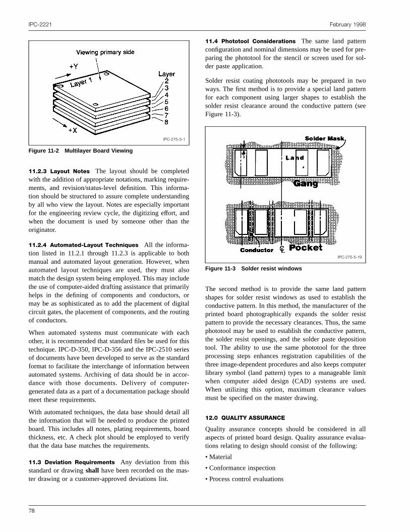
e-a-inntdth
thelsdriloitin
cthiedanorr-ou
l adrify
-
e-l-
ornthesee
rntheeistmern,ionetheuteritd.s
allua-
IPC-2221 February 1998
11.2.3 Layout Notes The layout should be completedwith the addition of appropriate notations, marking requirments, and revision/status-level definition. This informtion should be structured to assure complete understandby all who view the layout. Notes are especially importafor the engineering review cycle, the digitizing effort, anwhen the document is used by someone other thanoriginator.
11.2.4 Automated-Layout Techniques All the informa-tion listed in 11.2.1 through 11.2.3 is applicable to bomanual and automated layout generation. However, whautomated layout techniques are used, they must amatch the design system being employed. This may incluthe use of computer-aided drafting assistance that primahelps in the defining of components and conductors,may be as sophisticated as to add the placement of digcircuit gates, the placement of components, and the routof conductors.
When automated systems must communicate with eaother, it is recommended that standard files be used fortechnique. IPC-D-350, IPC-D-356 and the IPC-2510 serof documents have been developed to serve as the stanformat to facilitate the interchange of information betweeautomated systems. Archiving of data should be in accdance with those documents. Delivery of computegenerated data as a part of a documentation package shmeet these requirements.
With automated techniques, the data base should detaithe information that will be needed to produce the printeboard. This includes all notes, plating requirements, boathickness, etc. A check plot should be employed to verthat the data base matches the requirements.
11.3 Deviation Requirements Any deviation from thisstandard or drawingshall have been recorded on the master drawing or a customer-approved deviations list.
IPC-275-3-1
Figure 11-2 Multilayer Board Viewing
78
g
e
noeyralg
hissrd
-
ld
ll
d
11.4 Phototool Considerations The same land patternconfiguration and nominal dimensions may be used for prparing the phototool for the stencil or screen used for soder paste application.
Solder resist coating phototools may be prepared in twways. The first method is to provide a special land pattefor each component using larger shapes to establishsolder resist clearance around the conductive pattern (Figure 11-3).
The second method is to provide the same land patteshapes for solder resist windows as used to establishconductive pattern. In this method, the manufacturer of thprinted board photographically expands the solder respattern to provide the necessary clearances. Thus, the saphototool may be used to establish the conductive pattethe solder resist openings, and the solder paste deposittool. The ability to use the same phototool for the threprocessing steps enhances registration capabilities ofthree image-dependent procedures and also keeps complibrary symbol (land pattern) types to a manageable limwhen computer aided design (CAD) systems are useWhen utilizing this option, maximum clearance valuemust be specified on the master drawing.
12.0 QUALITY ASSURANCE
Quality assurance concepts should be considered inaspects of printed board design. Quality assurance evaltions relating to design should consist of the following:
• Material
• Conformance inspection
• Process control evaluations
IPC-275-5-19
Figure 11-3 Solder resist windows

bth
usif aesutiv
etesheoo
ins tanretediveg.,io
p-at isca
cifil isc-osfoi
ceodntioi
nnt
seendm
c,hisene--ce
-n-e-
er.
ind
e
ir
nle,nele
ntbe
-
re
February 1998 IPC-2221
This section defines the various specimen that shouldconsidered during the design process. Also included isrationale and purpose for the use of each specimen.
12.1 Conformance Test Specimen Conformance testspecimen, when required,shall be in accordance with thissection. Quality assurance provisions often require theof specific test procedures or evaluations to determineparticular product meets the requirements of the customor specifications. Some of the evaluations are done vially, others are done through destructive and nondestructesting.
Some quality evaluations are performed on test specimbecause the test is destructive or the nature of therequires a specific design which may not exist on tprinted board. Test specimen are used in these typestests as representatives of the printed boards fabricatedthe same panel.
A test specimen is a suitable sample for destructive testsince it has been subjected to the same processes aprinted boards on the same panel; however, the designlocation of the test specimen are critical in order to ensuthat the specimen are truly representative of the prinboards. A production board may be used for destructtests. Tests requiring specific circuit configuration (e.insulation resistance) may also be performed on productboards if appropriate circuitry is included in the design.
12.2 Material Quality Assurance Material inspectionsnormally consist of certification by the manufacturer suported by verifying data based on statistical sampling thall materials which become a part of the finished producin accordance with the master drawing, material specifitions, and/or procurement documentation.
Conformance specimen are defined in the detailed specations for the base material. As an example, copper foitested for tensile strength, ductility, elongation, fatigue dutility, peel strength, and carrier release strength. In minstances, the conformance test specimen for metalconsist of a specific length and width.
Laminate specifications, however, require conformanspecimen that relate more to performance of the end pruct board. Not only are peel strength, dielectric breakdowand water absorption tested, the methods of examinarequire that specific specimen geometries be preparedorder to make the test as meaningful as possible. Whedesign requires verification of the base material at the eproduct board level, conformance specimen are usedestablish that evaluation is identical or similar to thodefined in existing base material specifications. Some usmay require more than one ply of reinforcement agreater than 0.05 mm dielectric thickness. Example: So
ee
e
r-e
nt
fn
ghed
n
t
-
-
tl
-,nnado
rs
e
military specifications require two ply reinforcement andgreater than 0.09 mm dielectric thickness.
Each design sectional allows for a minimum dielectrithickness between layers of a multilayer printed boardwhen agreed upon between user and supplier. When trequirement is agreed upon, conformance test specimmust be provided as a part of the design to verify the spcific resin and resin content, glass style, dielectric withstanding voltage between claddings and moisture resistanverification.
12.3 Conformance Evaluations Conformance evalua-tions are performed on production boards and/or conformance specimen. If a production board is selected for coformance evaluation, it should be capable of meeting threquirements of Table 12-1. Specimen required for conformance evaluationshall be as defined herein. Additionalconformance specimen may be added by the manufacturConformance specimenshall be traceable to the productionpanel.
12.3.1 Specimen Quantity and Location The conform-ance test circuitry comprised of the specimen described12.4shall be a part of every panel used to produce printeboards when required by the performance specification.
All required configurations of the specimenshall bedefined on the master artwork and master drawing. Thlocation of the specimen on the production mastershall bepositioned within 6.4 mm and 12.7 mm of the printedboard image. The minimum number specimen and therequirement for location on the production mastershall bein accordance with Table 12-1. Figure 12-1 shows aexample of specimen location concepts. When feasibspecimen should also be located in the center of each pato reflect plating characteristics. Other specimen may bpositioned by the fabricator to optimize material utilizationand tooling provided the 6.4 mm and 12.7 mm requiremeis maintained. At least one hole in each specimen shouldlocated on the same grid as the printed board features.
12.3.2 Specimen Identification Conformance test cir-cuitry shall provide space for:
• Board part number and revision letter
• Traceability identification
• Lot date code
• Manufacturer’s identification, e.g., Commercial and Government Entity (CAGE), logo, etc.
Special coding systems may be used provided they aidentified on the master drawing.
79

IPC-2221 February 1998
Table 12-1 Specimen Frequency Requirements 1
Specimen Purpose I.D. 2 Class 1 Class 2 Class 3
Conformance Testing
Hole Solderability A Not Required Twice per panel Twice per panel
Solderability S Optional Optional Optional
Solder Resist Tenting(if used)
T Not required Once per panel with solderresist, location optional
Once per panel with solderresist, location optional
Thermal Stress, PlatingThickness, and BondStrength Type 1
B Twice per panel oppositecorners
Twice per panel oppositecorners
Twice per panel oppositecorners
Plating Adhesion andSurface Solderability
C Not Required Once per panel, locationoptional, pattern defined byartwork
Once per panel locationoptional, pattern defined byartwork
Solder Resist (if used) G Once per panel with solderresist, location optional
Once per panel with solderresist, location optional
Once per panel with solderresist, location optional
Surface Mount Solderability(Optional for SMT)
M Not required Once per panel, locationoptional, pattern defined byartwork
Once per panel, locationoptional, pattern defined byartwork
Reliability Assurance Inspection
Surface Mount BondStrength (Optional for SMT)
N Not Required Once per panel, locationoptional, pattern defined byartwork
Once per panel, locationoptional, pattern defined byartwork
Surface InsulationResistance
H Once per panel, locationoptional
Twice per panel oppositecorners
Twice per panel oppositecorners
Moisture and InsulationResistance
E Once per panel, locationoptional
Twice per panel, oppositecorners
Twice per panel oppositecorners
Optional or Process Control
Registration (Option 1 or 2) F Not required Four per panel, oppositesides defined by artwork
Four per panel, oppositesides defined by artwork
Registration (Optional) R Not required Four per panel, oppositesides defined by artwork
Four per panel, oppositesides defined by artwork
Interconnect Resistance(Optional 1 or 2)
D Not required Once per panel, locationoptional, pattern defined byartwork
Once per panel, locationoptional, pattern defined byartwork
1 If additional coupons for impedance testing are required, follow guidelines of IPC-D-317 and IPC-D-330.2 Where possible, coupon identification letters have been chosen to conform to those currently being used for conformance evaluations.
IPC-318-6
Figure 12-1 Location of test circuitry
Single Board Image
Artwork
Coupon Identification
TYP
6.35mm 12.7mm
Alternate Positions for Coupons
Test Coupons
Test Coupons Coupon Identification
Coupon F Location (TYP)
▼▼
▼ ▼ ▼▼
▼▼▼ ▼▼
Three Board Panel Nine Board Panel
oob
erac-gy,
12.3.3 General Specimen Requirements Test specimenshould reflect the specific board characteristics. This infmation consists of meeting the requirements for holes, cductors, spaces, etc. When specimen are used to estaprocess control parameters, theyshall consistently use a
80
r-n-lish
single hole size or land configuration which reflects thprocess. Process characteristics and general board chateristics should be matched (i.e., threshold technololeading edge technology, etc.).

in
lentoa-td
atef
ofa-l
srd
rAee
c
i-
h
ae
r
onng.h
re
s)
ed
ge-re
n-er-ci-to
d
2
February 1998 IPC-2221
12.3.3.1 Tolerances Tolerances for the fabrication oftest specimenshall be the same as those for the printedboard.
12.3.3.2 Etched Letters Etched letters shown on speci-men are for reference only.
12.3.3.3 Interlayer Connection Holes Whenever a mul-tilayer design incorporates interlayer connection holesthe form of blind or buried vias, specimen A, B, and Dshall be designed so as to incorporate these types of hoconnecting the appropriate layers. The individual specimedescription contains information on how these holes arebe incorporated. The specific number of holes for evalution should be a minimum of three in each individual tesspecimen with a minimum of two test specimen requireon each individual panel.
12.3.3.4 Metal Cores Whenever a multilayer designuses metal cores, the same core(s)shall be incorporatedinto the design of the specimen.
If the metal core(s) has interlayer connection holes thpass through the core without contact, the design of thspecimenshall be representative of that characteristic. Ithe hole contacts the core, that characteristicshall also berepresented in the specimen. The minimum numberholes for this evaluation are three per specimen withminimum of two specimen on each individual panel. Additional A and B specimen may be required for horizontamicrosections.
Composite printed boardsshall have separate specimen forthe top side board, the bottom side board, and the compoite board. The specimen for the composite printed boashall include the core material.
12.4 Individual Specimen Design Individual test speci-men are designed to evaluate specific individual characteistics of the printed boards they represent (see also IPC-22). Variations in specified coupon design must meet thintent of the original design and be representative of thboard.
12.4.1 Specimen A and B (Plated Hole Evaluation) Testspecimen A and B are used to evaluate plated hole charateristics.
Figure 12-2 shows the general configuration of the specmen. The nominal hole size for solderability testingshallbe the diameter of the smallest solder-coated hole on tboard and the nominal land sizeshall be the diameter ofthe land used for that hole. For thermal stress, the nominhole sizeshall be the diameter of the smallest hole and thnominal land sizeshall be the diameter of the land used forthat hole. The land shapeshall be the same as that used onthe printed board for these lands and holes. Plated laye
s
-
--
-
e
l
s
shall represent printed board design, e.g., ground tiesspecific layers, deleted non-functional lands, etc. Spacibetween holesshall be representative of the printed boardConductorsshall be included in between the holes on eacsignal layer. The direction of the conductorshall alternatefrom layer to layer on the x and y-axis as shown in Figu12-3. The conductor widthshall be representative of thesmallest line width in the design.
For internal layer connection holes (blind and buried viaa minimum of one additional A or B specimenshall beadded for each interconnection plating operation requirby the design.
12.4.2 Specimen C (Plating Adhesion and Surface Sol-derability) This specimen is used to evaluate platinadhesion and surface solderability to J-STD-003 requirments. The design of this specimen is shown in Figu12-4.
12.4.3 Specimen D (Interconnection Resistance andContinuity) Test specimen D is used to evaluate interconection resistance, continuity, correct lay-up, and other pformance criteria. See Figure 12-5 for an example of spemen D. Figure 12-6 shows the modification to be madespecimen D for buried vias.
12.4.3.1 Conformance Testing For conformance test-ing, the number of layers, lay-up, layer configuration, anuse of nonfunctional landsshall be modified to reflect theboard design. The land sizeshall be representative of theboard and the hole diametershall be the smallest in theassociated board with the exception of A1, A2, B1, and B
IPC-2221-12-2
Figure 12-2 Test Specimen A and B, mm
35.0
2.5 2 PL
17.5
25.5
7.5
14.0
Layer 1 Only Appropriate Specimen Number PL 2
.25 (REF) Border Layer 1 Only
2.5 2 PL
2.5 2 PL 4.5
A B
��(35.0)
(14.0)
.500 4 PL
.500 2 PL
PLANE LAYERS
81
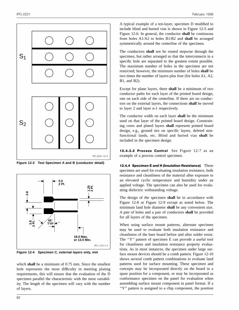
stgD
bir
tond
ein aible.not
2,
ign,uc-
in-
on-
ulke toanalu-
he.
enandsist.lua-sur--10andandaasenIf an
IPC-2221 February 1998
which shall be a minimum of 0.75 mm. Since the smallehole represents the most difficulty in meeting platinrequirements, this will ensure that the evaluation of thespecimen parallel the characteristic with the most variaity. The length of the specimen will vary with the numbeof layers.
IPC-2221-12-3
Figure 12-3 Test Specimen A and B (conductor detail)
S1
S2
IPC--275-7-4
Figure 12-4 Specimen C, external layers only, mm
▼
▼
18.0 Max. or 13.0 Min.
▼
▼
▼
▼
▼
▼ ▼
▼ ▼
▼
1.25
2
Pl.
5.0 2 Pl.
3.8
3.8
2 P
l. 45° TYP
82
l-
A typical example of a ten-layer, specimen D modifiedinclude blind and buried vias is shown in Figure 12-5 aFigure 12-6. In general, the conductorshall be continuousfrom holes A1/A2 to holes B1/B2 andshall be arrangedsymmetrically around the centerline of the specimen.
The conductorsshall not be routed stepwise through thspecimen, but rather arranged so that the interconnectsspecific hole are separated to the greatest extent possThe maximum number of holes in the specimen arerestricted; however, the minimum number of holesshall betwo times the number of layers plus four (for holes A1, AB1, and B2).
Except for plane layers, thereshall be a minimum of twoconductor paths for each layer of the printed board desone on each side of the centerline. If there are no condtors on the external layers, the connectionsshall be movedto layer 2 and layer n-1 respectively.
The conductor width on each layershall be the minimumused on that layer of the printed board design. Constraing cores and plated layersshall represent printed boarddesign, e.g., ground ties on specific layers, deleted nfunctional lands, etc. Blind and buried viasshall beincluded in the specimen design.
12.4.3.2 Process Control See Figure 12-7 as anexample of a process control specimen.
12.4.4 Specimen E and H (Insulation Resistance) Thesespecimen are used for evaluating insulation resistance, bresistance and cleanliness of the material after exposuran elevated cyclic temperature and humidity underapplied voltage. The specimen can also be used for evating dielectric withstanding voltage.
The design of the specimenshall be in accordance withFigure 12-8 or Figure 12-9 except as noted below. Tminimum land hole diametershall be any convenient sizeA pair of holes and a pair of conductorsshall be providedfor all layers of the specimen.
When using surface mount patterns, alternate specimmay be used to evaluate both insulation resistancecleanliness of the bare board before and after solder reThe ‘‘Y’’ pattern of specimen E can provide a useful toofor cleanliness and insulation resistance property evaltions. As in most instances, the specimen under largeface mount devices should be a comb pattern. Figure 12shows several comb pattern combinations to evaluate lpatterns used for surface mounting. These specimenconcepts may be incorporated directly on the board inspare position for a component, or may be incorporatedconformance specimen on the panel for evaluation whassembling surface mount component in panel format.‘‘Y’’ pattern is assigned to a chip component, the positio
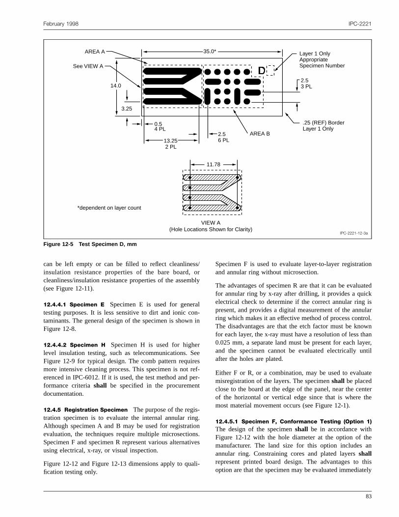
February 1998 IPC-2221
IPC-2221-12-3a
Figure 12-5 Test Specimen D, mm
11.78
VIEW A (Hole Locations Shown for Clarity)
*dependent on layer count
D14.0
35.0*
13.25 2 PL
2.5 6 PL
3.25
0.54 PL
AREA B
2.5 3 PL
Layer 1 Only Appropriate Specimen Number
.25 (REF) Border Layer 1 Only
AREA A
See VIEW A
s/ob
lnn i
reesrefert
gonnsive
li-
ion
atedkisularol.ownanyer,ntil
ate
nterhe
hean
thistely
can be left empty or can be filled to reflect cleanlinesinsulation resistance properties of the bare board,cleanliness/insulation resistance properties of the assem(see Figure 12-11).
12.4.4.1 Specimen E Specimen E is used for generatesting purposes. It is less sensitive to dirt and ionic cotaminants. The general design of the specimen is showFigure 12-8.
12.4.4.2 Specimen H Specimen H is used for highelevel insulation testing, such as telecommunications. SFigure 12-9 for typical design. The comb pattern requirmore intensive cleaning process. This specimen is noterenced in IPC-6012. If it is used, the test method and pformance criteriashall be specified in the procuremendocumentation.
12.4.5 Registration Specimen The purpose of the regis-tration specimen is to evaluate the internal annular rinAlthough specimen A and B may be used for registratievaluation, the techniques require multiple microsectioSpecimen F and specimen R represent various alternatusing electrical, x-ray, or visual inspection.
Figure 12-12 and Figure 12-13 dimensions apply to quafication testing only.
��
rly-n
e
--
.
.s
Specimen F is used to evaluate layer-to-layer registratand annular ring without microsection.
The advantages of specimen R are that it can be evalufor annular ring by x-ray after drilling, it provides a quicelectrical check to determine if the correct annular ringpresent, and provides a digital measurement of the annring which makes it an effective method of process contrThe disadvantages are that the etch factor must be knfor each layer, the x-ray must have a resolution of less th0.025 mm, a separate land must be present for each laand the specimen cannot be evaluated electrically uafter the holes are plated.
Either F or R, or a combination, may be used to evalumisregistration of the layers. The specimenshall be placedclose to the board at the edge of the panel, near the ceof the horizontal or vertical edge since that is where tmost material movement occurs (see Figure 12-1).
12.4.5.1 Specimen F, Conformance Testing (Option 1)The design of the specimenshall be in accordance withFigure 12-12 with the hole diameter at the option of tmanufacturer. The land size for this option includesannular ring. Constraining cores and plated layersshallrepresent printed board design. The advantages tooption are that the specimen may be evaluated immedia
��
83
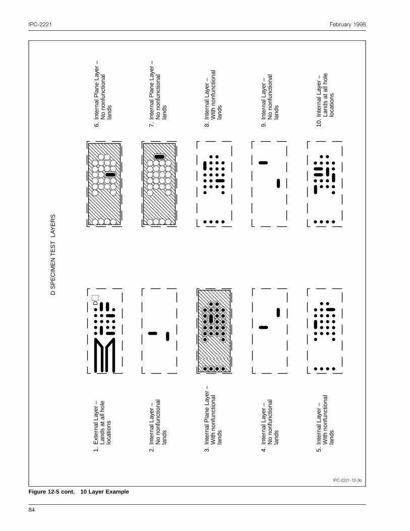
IPC-2221 February 1998
IPC-2221-12-3b
Figure 12-5 cont. 10 Layer Example
����
D
D S
PE
CIM
EN
TE
ST
LAY
ER
S
1.E
xter
nal L
ayer
–
La
nds
at a
ll ho
le
lo
catio
ns
2.I
nter
nal L
ayer
–
N
o no
nfun
ctio
nal
la
nds
3.I
nter
nal P
lane
Lay
er –
With
non
func
tiona
l
land
s 4.
Int
erna
l Lay
er –
No
nonf
unct
iona
l
land
s 5.
Int
erna
l Lay
er –
With
non
func
tiona
l
land
s
6.I
nter
nal P
lane
Lay
er –
No
nonf
unct
iona
l
land
s
7.I
nter
nal P
lane
Lay
er –
No
nonf
unct
iona
l
land
s 8.
Int
erna
l Lay
er –
With
non
func
tiona
l
land
s 9.
Int
erna
l Lay
er –
No
nonf
unct
iona
l
land
s 10
.Int
erna
l Lay
er –
Land
s at
all
hole
loca
tions
84
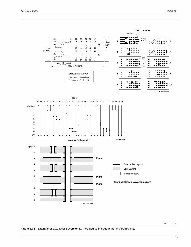
February 1998 IPC-2221
IPC-2221-12-4
Figure 12-6 Example of a 10 layer specimen D, modified to include blind and buried vias
IPC-I-002036
1.25mm Typical
1.25mm Typical
1.75mm Clearance
Typical
Plane Layer
Pl a
n e
L a y e r
Pl a
n e
L a y e r
6.
7.
8.
9.
10.
▼▼
▼
▼
▼
TEST LAYERS.
1.
2.
3.
4.
5.
▼
▼
▼ ▼27.5mm [1.100"]
▼ ▼7.5 [0.300"]
12.5 [0.500"]
▼
▼
2.5mm [0.100"] TYP
A
A
1
2
B
B
2
1
+
+
+
+
01 02 05 06 09 10
24 23 20 19 16 15
12
13
03 04 07 08 11
22 21 18 17 14
24 holes in daisy chain
4 holes (A A B B )1 2 1 2
28 HOLES IN COUPON
Layer: 1
2
3
4
5
6
7
8
9
10
Conductive Layers
Core Layers
B-Stage Layers
Representative Layer Diagram
IPC-I-002133
Plane
Plane
Plane
IPC-I-002133
1
2
3
4
5
6
7
8
9
10
A1 A2 1 2 3 4 5 6 7 8 9 10 11 12 13 14 15 16 17 18 19 20 21 22 23 24 B2 B1
Hole:
Layer:
Wiring Schematic
85
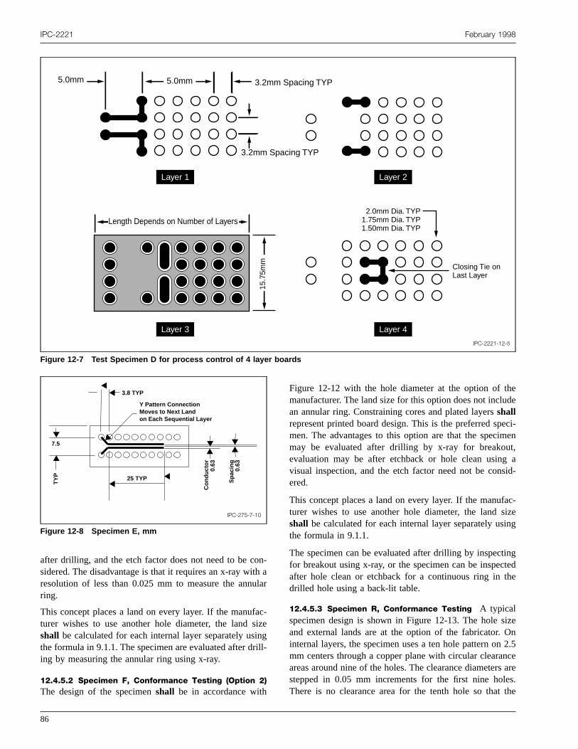
IPC-2221 February 1998
IPC-2221-12-5
Figure 12-7 Test Specimen D for process control of 4 layer boards
5.0mm
Length Depends on Number of Layers
5.0mm
3.2mm Spacing TYP
3.2mm Spacing TYP
Layer 1
Layer 3
Layer 2
Layer 4
15.7
5mm
2.0mm Dia. TYP 1.75mm Dia. TYP 1.50mm Dia. TYP
Closing Tie on Last Layer
onithula
facsizsingrill
ee
ci-en,aid-
c-izeg
gede
zen2.5ceares.he
after drilling, and the etch factor does not need to be csidered. The disadvantage is that it requires an x-ray wresolution of less than 0.025 mm to measure the annring.
This concept places a land on every layer. If the manuturer wishes to use another hole diameter, the landshall be calculated for each internal layer separately uthe formula in 9.1.1. The specimen are evaluated after ding by measuring the annular ring using x-ray.
12.4.5.2 Specimen F, Conformance Testing (Option 2)The design of the specimenshall be in accordance with
IPC-275-7-10
Figure 12-8 Specimen E, mm
▼
▼
▼▼
TY
P 25 TYP
▼
▼ ▼
Y Pattern Connection Moves to Next Land on Each Sequential Layer
▼
Co
nd
uct
or
Sp
acin
g0.
63
3.8 TYP
▼▼ ▼
0.63
7.5
86
-ar
-e
-
Figure 12-12 with the hole diameter at the option of thmanufacturer. The land size for this option does not includan annular ring. Constraining cores and plated layersshallrepresent printed board design. This is the preferred spemen. The advantages to this option are that the specimmay be evaluated after drilling by x-ray for breakoutevaluation may be after etchback or hole clean usingvisual inspection, and the etch factor need not be consered.
This concept places a land on every layer. If the manufaturer wishes to use another hole diameter, the land sshall be calculated for each internal layer separately usinthe formula in 9.1.1.
The specimen can be evaluated after drilling by inspectinfor breakout using x-ray, or the specimen can be inspectafter hole clean or etchback for a continuous ring in thdrilled hole using a back-lit table.
12.4.5.3 Specimen R, Conformance Testing A typicalspecimen design is shown in Figure 12-13. The hole siand external lands are at the option of the fabricator. Ointernal layers, the specimen uses a ten hole pattern onmm centers through a copper plane with circular clearanareas around nine of the holes. The clearance diametersstepped in 0.05 mm increments for the first nine holeThere is no clearance area for the tenth hole so that t

February 1998 IPC-2221
IPC-2221-12-6
Figure 12-9 Optional Specimen H, mm
����Layer 1 Only Appropriate Specimen Number
H
6.0
DIM C 9 PL
3.375 2 PL
1.0 2 PL
2.5 18 PL
35.0 1.4 Land Diameter 20 PL
1.0 10 PL
2.0 2PL
DIM B 10 PL
DIM A 2 PL
28.0
1.0 2PL
2.0 2 PL
2.0 2 PL
6.5.25 (REF) Border Layer 1 Only
One Connection Per Layer (Top and Bottom) Starting With Layer 1 On The Left
Example: Connection To Comb Pattern On Layer 3 Is Third From Left
IPC-275-7-11
Figure 12-10 Comb pattern examples
87

cmg4
+
enX
er
ftor
too
thr
inin
ftenbeaa-of
iod
toci-est
toface12.
teionis
isod-
sedthethatn
hef-er-t
cessThethepe-to
sys-ol.
enci-rer.
IPC-2221 February 1998
hole will make contact with the plane. The center clearanareashall be designed for the worst case hole-to-pad diaeter difference for the layer. Since the manufacturinallowance may vary from layer-to-layer, see Figure 12-1the diameter of the artwork center clearance areashall becalculated for each internal layer separately as follows:
Clearance diameter = nominal drilled hole diametermanufacturing allowance
Manufacturing allowance = smallest difference betweany functional plated hole and land on that layer - 2annular ring.
Evaluation of the specimen can only take place after detmining the etch factor for each layer. The etch factorshallbe determined before lamination as follows:
Etch loss = the diameter of the center clearance area aetch - the diameter of the center clearance on the artw
The reference hole for annular ring evaluation will bethe left or the right of the center clearance area basedthe etch factor. For example: If the etch factor is +0.1 mmthe reference holeshall be two holes to the right of thecenter clearance area. If the etch factor is -0.05 mm,reference holeshall be one hole to the left of the centeclearance area.
The specimen can be evaluated after drilling by measurthe annular ring using x-ray. To accept the specimen usx-ray, the reference holeshall not touch the plane.
The specimen are designed to measure annular ring athe holes are plated. The specimen are acceptable if this no electrical connection between the reference hole athe tenth hole. The dimension of the annular ring candetermined by finding the first hole which makes electricconnection to the tenth hole and noting its position in reltion to the reference hole. Each hole to the left or rightthe reference hole represents a + 0.025 mm or -0.025 mmrespectively to the reference annular ring. This specimennot referenced in IPC-6012. If it is used, the test methand performance criteriashall be specified in the procure-ment documentation.
IPC-275-7-12
Figure 12-11 ‘‘Y’’ pattern for chip component cleanlinesstest pattern
88
e-
,
-
erk
n,
e
gg
erred
l
s
12.4.6 Specimen G (Solder Resist Adhesion) The testspecimen for evaluating solder resist adhesionshall be asshown in Figure 12-15. The artworkshall provide for sol-der resist to cover the entire specimen.
12.4.7 Specimen M (Optional) The specimenshall be asshown in Figure 12-16. This specimen may be usedevaluate solderability of surface mount lands This spemen is not referenced in IPC-6012. If it is used, the tmethod and performance criteriashall be specified in theprocurement documentation.
12.4.8 Specimen N (Optional) Specimenshall be asshown in Figure 12-17. This specimen may be usedevaluate the bond strength and peel strength of surmount lands. This specimen is not referenced in IPC-60If it is used, the test method and performance criteriashallbe specified in the procurement documentation.
12.4.9 Specimen S This specimen is used to evaluaplated-through hole solderability when a larger populatof holes is required. The general design of the couponshown in Figure 12-18. The hole diametershall be 0.8 mm± 0.13 mm required to be solder filled. This specimennot referenced in IPC-6012. If it is used, the test methand performance criteriashall be specified in the procurement documentation.
12.4.10 Specimen T This specimenshall be used tovalidate tenting characteristics when solder resists are uto tent plated-through holes (see 4.5.1). Specimen T issame as shown in Figure 12-18 (specimen S) exceptthe entire specimenshall be covered with solder resist oboth sides.
The hole diametershall be the largest plated hole whicwill be tented with solder resist. This specimen is not rerenced in IPC-6012. If it is used, the test method and pformance criteriashall be specified in the procuremendocumentation.
12.4.11 Process Control Test Specimen Process con-trol test specimen are used at strategic points in the proflow to evaluate a specific process or set of processes.designs of the process control test specimen are atoption of the printed board fabricator. Each design is scific to the processes for which the fabricator intendsevaluate.
Process control evaluations are established through atematic path for implementing statistical process contrThis includes those items shown in Figure 12-19.
If the contract permits the use of process control specimin lieu of conformance specimen, the design of the spemenshall be agreed to between the user and manufactu
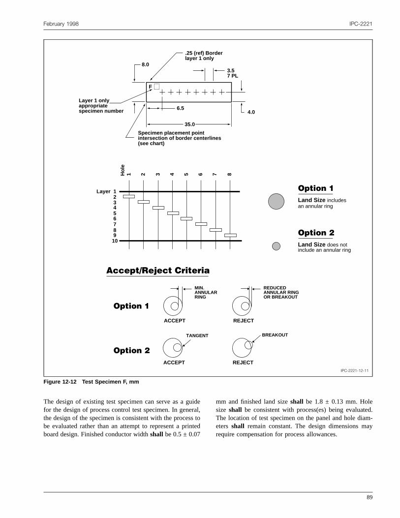
February 1998 IPC-2221
IPC-2221-12-11
Figure 12-12 Test Specimen F, mm
ACCEPT
ACCEPT REJECT
BREAKOUTTANGENT
MIN. ANNULAR RING
Layer 12345678910
1 2Ho
le
3 4 5 6 7 8
Option 1Land Size includes an annular ring
Option 2Land Size does not include an annular ring
Accept/Reject Criteria
REJECT
REDUCED ANNULAR RING OR BREAKOUT
Option 1
Option 2
F
6.5
35.0
8.0
4.0
3.5 7 PL
.25 (ref) Border layer 1 only
Layer 1 only appropriate specimen number
Specimen placement point intersection of border centerlines (see chart)
idras tte
d.m-y
The design of existing test specimen can serve as a gufor the design of process control test specimen. In genethe design of the specimen is consistent with the procesbe evaluated rather than an attempt to represent a prinboard design. Finished conductor widthshall be 0.5 ± 0.07
el,od
mm and finished land sizeshall be 1.8 ± 0.13 mm. Holesize shall be consistent with process(es) being evaluateThe location of test specimen on the panel and hole diaetersshall remain constant. The design dimensions marequire compensation for process allowances.
89
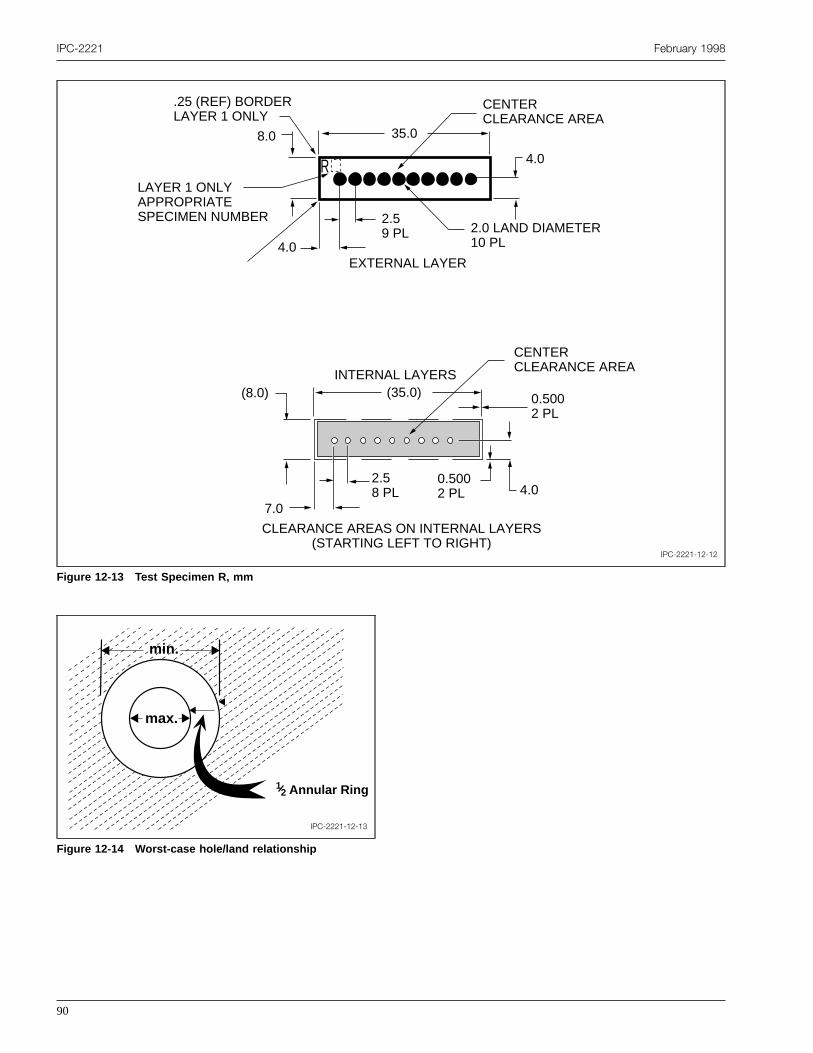
IPC-2221 February 1998
IPC-2221-12-12
Figure 12-13 Test Specimen R, mm
R
.25 (REF) BORDER LAYER 1 ONLY
8.0 35.0
LAYER 1 ONLY APPROPRIATE SPECIMEN NUMBER 2.5
9 PL
4.0
2.0 LAND DIAMETER 10 PL4.0
EXTERNAL LAYER
CENTER CLEARANCE AREA
INTERNAL LAYERS(35.0)(8.0) 0.500
2 PL
2.5 8 PL
0.500 2 PL 4.0
7.0
CLEARANCE AREAS ON INTERNAL LAYERS (STARTING LEFT TO RIGHT)
CENTER CLEARANCE AREA
IPC-2221-12-13
Figure 12-14 Worst-case hole/land relationship
max.▼ ▼
▼▼
min.▼ ▼
Annular Ring12
90

February 1998 IPC-2221
IPC-2221-12-13a
Figure 12-15 Test Specimen G, mm
IPC-275-7-5
Figure 12-16 Test Specimen M, surface mounting solderability testing, mm
32.0mm
25.4mm
2.5mm
7.0mm
2.5mm
12.5mm
6.0mm 2 Pl.
1.9mm 2 PL
91
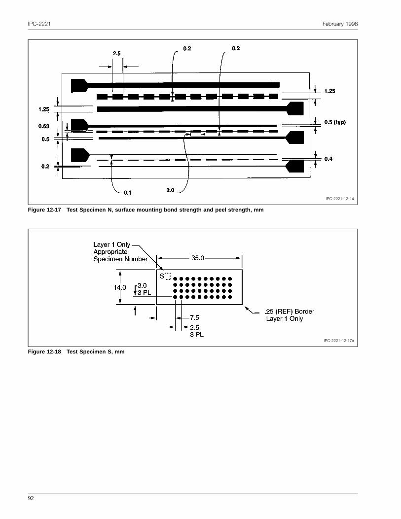
IPC-2221 February 1998
IPC-2221-12-14
Figure 12-17 Test Specimen N, surface mounting bond strength and peel strength, mm
IPC-2221-12-17a
Figure 12-18 Test Specimen S, mm
92
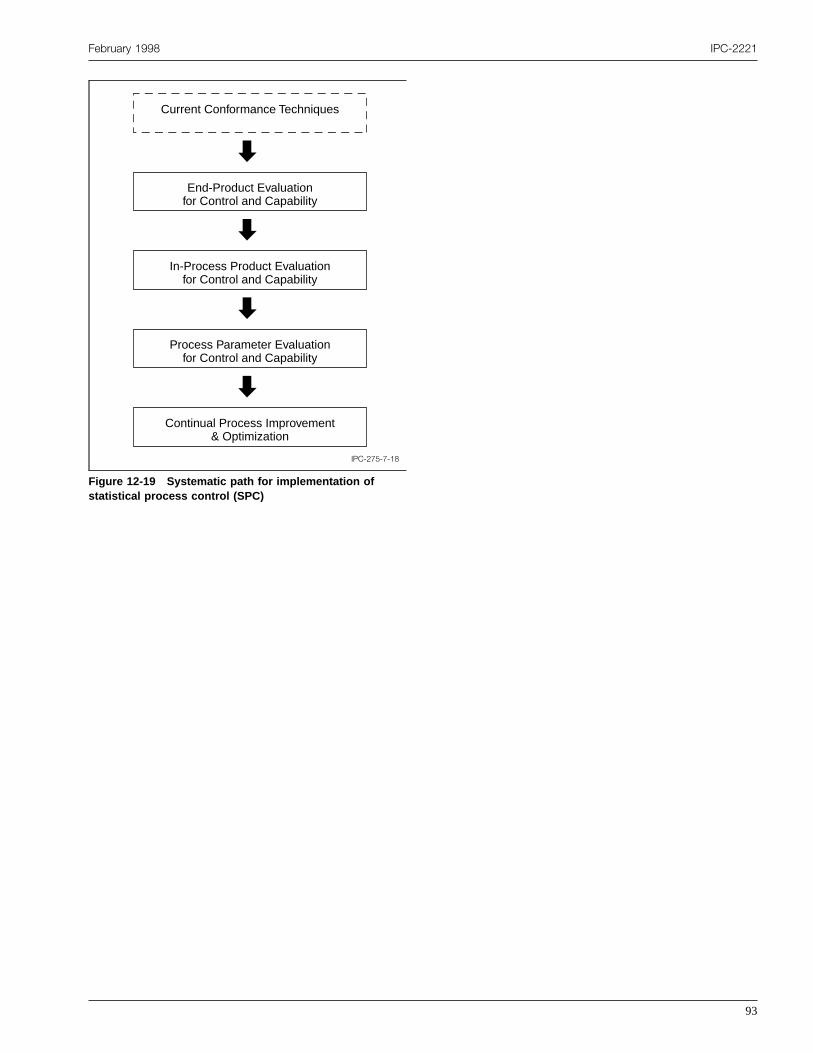
February 1998 IPC-2221
IPC-275-7-18
Figure 12-19 Systematic path for implementation ofstatistical process control (SPC)
Current Conformance Techniques
End-Product Evaluation for Control and Capability
In-Process Product Evaluation for Control and Capability
Process Parameter Evaluation for Control and Capability
Continual Process Improvement & Optimization
93

IPC-2221 February 1998
Appendix AExample of a Testability Design Checklist
nst
-
ge
u
lex
n
ut
ec
a
le
g
os
o
r
d.
o
le
et
o
uit
in
ral
hena
st-
er-
the
rks
gera-
ver
-
y
uithat
ir-on-
g,
an
p-
y
ise
• Route test/control points edge connector to enable motoring and driving of internal board functions and to assiin fault diagnosis.
• Divide complex logic functions into smaller, combinational logic sections.
• Avoid one-shots; if used, route their signals to the edconnector.
• Avoid potentiometers and ‘‘select-on-test’’ components.
• Use a single, large-edge connector to provide input/outppins and test/control points.
• Make printed board input/output signal logic-compatibto keep test equipment interface costs low and give fleibility.
• Provide adequate decoupling at the board edge alocally at each integrated circuit.
• Provide signals leaving the board with maximum fan-odrive, or buffer them.
• Buffer edge-sensitive components from the edge conntor - such as clock lines and flip-flop outputs.
• Do not tie signal outputs together.
• Never exceed the logic rated fan-out; in fact, keep it tominimum.
• Do not use high fan-out logic devices. do use multipfan-out devices, and keep their outputs separate.
• Keep logic depth on any board to a low level by usinedge terminated test/control points.
• Single-load each signal entering the board whenever psible.
• Terminate unused logic pins with a resistive pull-up tminimize noise pick-up.
• Do not terminate logic outputs directly into transistobases. do use a series current-limiting resistor.
• Buffer flip-flop output signals before they leave the boar
• Use open-collector devices with pull-up resistors tenable external override control.
• Avoid using redundant logic to minimize undetectabfaults.
• Bring outputs of cascaded counters to higher- ordcounters so that they can be tested without large coun
• Construct trees to check the parity of selected groupseight bits or fewer.
• Avoid ‘‘wired’OR’’ and ‘‘wired’AND’’ connections.
94
i-
t
-
d
-
-
rs.
f
• If you cannot, use gates from the same integrated circpackage.
• Provide some way to bypass level-changing diodesseries with logic out-puts.
• Break paths when a logic element fans out to seveplaces that converge later.
• Use elements in the same integrated circuit package wdesigning a series of inverters or inverters followinggate function.
• Standardize power-on and ground pins to avoid teharness multiplicity.
• Bring out test points as near to digital-to-analog convsion as possible.
• Provide a means of disabling on-board clocks so thattester clock may be substituted.
• Provide mounted switches and resistor-capacitor netwowith override lines to the edge-board connector.
• Route logic drivers of lamps and displays to the edconnector so that the tester can check for correct opetion.
• Divide large printed boards into subsections whenepossible, preferably by function.
• Separate analog circuits from digital logic, except for timing circuits.
• Uniformly mount integrated circuits and clearly identifthem to make it easier to locate them.
• Provide sufficient clearance around integrated circsockets and direct-soldered integrated circuits so tclips can be attached whenever necessary.
• Add top-hat connector pins or mount extra integrated ccuit sockets when there are not enough edge-board cnector pins for test/control points.
• Use sockets with complex integrated circuits and londynamic shift registers.
• Wire feedback lines and other complex circuit lines to
• Use jumpers that can be cut during debugging. The jumers can be located near the edge-board connector.
• Fix locations of power and ground lines for uniformitamong several board types.
• Make the ground conductor large enough to avoid noproblems.
• Group together signal lines of particular families.
• Clearly label all parts, pins and connectors.

February 1998 IPC-2221
INDEX
pe-rga
.2.6
The following is an index of key subjects related to scific paragraph numbers in this standard. The index is onized alphabetically.AAdhesive Films or Sheets 4.2.3Altitude Effects 7.1.4Annular Ring Requirements 9.1.2Array SMT 8.6Aspect Ratio 9.2.6Assembly and Test 5.3.3Assembly Requirements 5.3Attachment Requirements 8.2Automated-layout Techniques 11.2.4Automatic Assembly 8.1.1Axial Leaded Components 8.3.1.6
BBare Board Fabrication 5.1.1Bare Board Testing 3.5.6.1Bare Die 8.7Blind and Buried Vias 9.2.7Blind and Buried Vias Hole Size 9.2.7.3Blind Vias 9.2.7.1Board Geometries (Size and Shape) 5.2.3Board Layout Design 3.6.1Board Size 5.2.2Board Type 5.2.1Board Type Classification 1.6.1Bonding Material 4.2.1Boundary Scan Testing 3.5.2Bow and Twist 5.2.4Buried Capacitors 4.4.10.2Buried Resistors 4.4.10.1Buried Vias 9.2.7.2Bus Bar 8.2.13
C
Capacitance Considerations 6.4.5Chip Scale 8.7.3Circuit Type Considerations 6.1.3Classification of Products 1.6Clinched Leads 8.3.1.3Color Pigmentation 4.3.1Component Accessibility 8.1.4Component and Assembly Issues 8.0Component and Feature Location 5.4.2Component Body Centering 8.1.6Component Clearances 8.1.8Component Lead Sockets 8.4.5Component Orientation 8.1.3Component Placement 8.1.2
-Composite (Constraining-core) Boards 5Conduction 7.1.1Conductive Dielectric Composites 4.4.11Conductive Materials 4.4Conductor Characteristics 10.1Conductor Routing 10.1.3Conductor Spacing 10.1.4Conductor Width and Thickness 10.1.1Conformal Coatings 4.5.2Conformance Evaluations 12.3Conformance Test Specimen 12.1Connectors and Interconnects 8.2.5Convection 7.1.3Cooling Mechanisms 7.1Copper Film 4.4.9.2Copper Foil 4.4.9.1
DDatum Features 5.4.3Design Envelope 8.1.5Design Layout 3.2Deviation Requirements 11.3Dielectric Base Materials 4.2Dielectric Thickness/Spacing 4.3.2Dimensioning Systems 5.4Dimensions and Tolerances 5.4.1Documentation 11.0Dual In-line Connectors 8.2.5.2Dual In-line Packages 8.3.1.5
EEdge-Board Adapter Connectors 8.2.5.6Edge-Board Connectors 8.2.5.3Electrical Clearance 6.3, 10.1.2Electrical Considerations 6.1Electrical Performance 6.1.1Electrical Properties 6.0Electrical Testing 3.5.6Electroless Copper Plating 4.4.1Electrolytic Copper Plating 4.4.3Electronic Component Materials 4.4.10Embedded Microstrip 6.4.2End-Product Requirements 3.2.1Environmental Testing 3.5.7ESD Considerations 4.6.1Etched Letters 12.3.3.2Eyelets 8.2.10
F
Fabrication Considerations 5.1Fastening hardware 8.2.6Feasibility Density Evaluation 3.6.2
95

3
8
.21.2
IPC-2221 February 1998
Fine Pitch SMT 8.5Flat-pack Components 8.4.2Flat-Packs 8.3.1.9Flexible Cable 8.2.14Flip Chip 8.7.2Foils/Film 4.4.9.3Functional Test for Printed Board Assemblies 3.5.Fuzz Button 8.10.1
GGeneral Circuit Feature Requirements 10.0General Requirements 3.0Gold Plating 4.4.4
HHeat Dissipation Considerations 7.2, 8.1.10Heat Shrinkable Devices 8.2.12Heat Transfer Techniques 7.3Hole Location 9.2.1Hole Location Tolerances 9.2.2Hole Pattern Variation 9.2.5Hole Quantity 9.2.3Holes 9.2Holes/Interconnections 9.0Impedance and Capacitance Control 6.4
IIn-Circuit Electrical Considerations 3.5.4.2In-Circuit Test 3.5.4Individual Component Heat Dissipation 7.2.1Individual Specimen Design 12.4Information Hierarchy 3.1Initialization and Synchronization 3.5.3.2Interlayer Connection Holes 12.3.3.3
JJumper Wires 8.2.11.1
LLaminate Materials 4.3Land Characteristics 10.2Land Requirements 9.1.1Lands for Flattened Round Leads 8.2.8, 9.1.4Lands for Surface Mounting 10.2.2Lands with Holes 9.1Large Conductive Areas 10.3Layout 11.2Layout Accuracy and Scale 11.2.2Layout Concepts 3.6.1.1Layout Evaluation 3.6Layout Notes 11.2.3Layout Viewing 11.2.1Leads Mounted in Through-Holes 8.3.1Long Counter Chains 3.5.3.3
MManufacturing Allowances 10.2.1Marking and Legends 4.6
96
Material Quality Assurance 12.2Material Selection 4.1Material Size 5.2.3.1Materials 4.0Mechanical Hardware Attachment 5.3.1Mechanical Testing 3.5.5Mechanical/Physical Properties 5.0Metal Core Substrates 4.4.9.4Metal Cores 12.3.3.4Metal Power Packages 8.3.1.10Metallic Coatings for Edgeboard Contacts 4.4.Metallic Foil/Film 4.4.9Microstrip 6.4.1Mounting Over Conductive Areas 8.1.7
NNickel Plating 4.4.5
OOne-Part Connectors 8.2.5.1Order of Precedence 3.1.1Organic Protective Coatings 4.5Orientation Symbols 10.2.4
PPart Support 5.3.2Partially Clinched Leads 8.3.1.4Parts List 3.4Performance Classes 1.6.2Performance Requirements 3.7Perpendicular (Vertical) Mounting 8.3.1.8Phototool Considerations 11.4Physical Support 8.1.9Physical Test Concerns 3.5.3.5Placement Requirements 8.1Plated-Through Hole Tolerances 9.2.6.1Plating Thieves 10.1.5Point of Origin 3.5.6.4Power Distribution Considerations 3.5.5.2, 6.1Preimpregnated Bonding Layer (Prepreg) 4.2.Pressure Contacts 8.1Process Control 12.4.3.2Process Control Test Specimen 12.4.11Producibility Level 1.6.3Product/Board Configuration 5.2
QQuality Assurance 12.0
RRadial-Lead Components 8.3.1.7Radiation 7.1.2Registration Specimen 12.4.5Resist Adhesion and Coverage 4.5.1.1Resist Clearance 4.5.1.2

.1
February 1998 IPC-2221
Ribbon Lead Termination 8.4.3Round Lead Termination 8.4.4
SSchematic/Logic Diagram 3.3Self Diagnostics 3.5.3.4Semiconductive Coatings 4.4.2Shock and Vibration 8.1.9.1Solder Coating 4.4.7Solder Resist (Solder Mask) Coatings 4.5.1Solder Terminals 8.2.9Solderball 8.9Soldering Considerations 8.2.4Spacing of Adjacent Holes 9.2.4Special Tooling 11.1Special Wiring 8.2.11Specimen A and B 12.4.1Specimen C 12.4.2Specimen D 12.4.3Specimen E and H 12.4.4Specimen F 12.4.5.1, 12.4.5.2Specimen G 12.4.6Specimen Identification 12.3.2Specimen M 12.4.7Specimen N 12.4.8Specimen Quantity and Location 12.3.1Specimen R 12.4.5.3Specimen Requirements 12.3.3Specimen S 12.4.9Specimen T 12.4.10Stiffeners 8.2.7Straight Through-Hole Mounted Leads 8.3.1Stress Relief 8.1.11Stripline Properties 6.4.3Stripline Properties, Asymmetric 6.4.4Structural Strength 5.2.5Surface Mount Requirements 8.4Surface-Mounted Leaded Components 8.4.1
TTape Automated Bonding 8.8Tarnish Protective Coatings 4.5.3Terminal Mounting-Electrical 8.2.9.2Terminal Mounting-Mechanical 8.2.9.1Test Connectors 3.5.3.1Test Points 3.5.6.5, 10.2.3Test Requirement Considerations 3.5Testability of Assembly 3.5.1Testing of Paired Boards 3.5.6.3Testing Surface Mount Patterns 3.5.6.2Thermal Design Reliability 7.4Thermal Management 7.0Thermal Matching 7.3.3Thermal Relief in Conductor Planes 9.1.3Thermal Transfer 7.3.2Through-Hole Requirements 8.3Tin Plating 4.4.6.1Tolerances 12.3.3.1Two-Part Discrete-Contact Connectors 8.2.5.5Two-Part Multiple Connectors 8.2.5.4
UUnclinched Leads 8.3.1.2Uniformity of Connectors 3.5.5.1
VVertical Mounting 8.3.1.8Vibration Design 5.2.7
WWire Bond 8.7.1Wires/Leads Attachment to Terminals 8.2.9.3
97

This page intentionally left blank
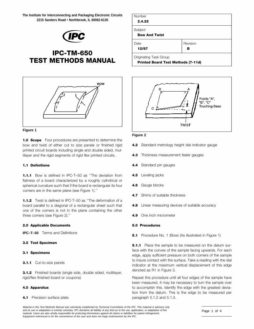
1.0 Scope Four procedures are presented to determine thebow and twist of either cut to size panels or finished rigidprinted circuit boards including single and double sided, mul-tilayer and the rigid segments of rigid flex printed circuits.
1.1 Definitions
1.1.1 Bow is defined in IPC-T–50 as ‘‘The deviation fromflatness of a board characterized by a roughly cylindrical orspherical curvature such that if the board is rectangular its fourcorners are in the same plane (see Figure 1).’’
1.1.2 Twist is defined in IPC-T–50 as ‘‘The deformation of aboard parallel to a diagonal of a rectangular sheet such thatone of the corners is not in the plane containing the otherthree corners (see Figure 2).’’
2.0 Applicable Documents
IPC–T–50 Terms and Definitions
3.0 Test Specimen
3.1 Specimens
3.1.1 Cut-to-size panels
3.1.2 Finished boards (single side, double sided, multilayer,rigid/flex finished board or coupons)
4.0 Apparatus
4.1 Precision surface plate
Figure 1
BOW
2 1
The Institute for Interconnecting and Packaging Electronic Circuits2215 Sanders Road • Northbrook, IL 60062-6135
IPC-TM-650TEST METHODS MANUAL
Material in this Test Methods Manual was voluntarily established by Technical Committees of theand its use or adaptation is entirely voluntary. IPC disclaims all liability of any kind as to the usematerial. Users are also wholly responsible for protecting themselves against all claims or liabilitEquipment referenced is for the convenience of the user and does not imply endorsement by th
4.2 Standard metrology height dial indicator gauge
4.3 Thickness measurement feeler gauges
4.4 Standard pin gauges
4.5 Leveling jacks
4.6 Gauge blocks
4.7 Shims of suitable thickness
4.8 Linear measuring devices of suitable accuracy
4.9 One inch micrometer
5.0 Procedures
5.1 Procedure No. 1 (Bow) (As illustrated in Figure 1)
5.1.1 Place the sample to be measured on the datum sur-face with the convex of the sample facing upwards. For eachedge, apply sufficient pressure on both corners of the sampleto insure contact with the surface. Take a reading with the dialindicator at the maximum vertical displacement of this edgedenoted as R1 in Figure 3.
Repeat this procedure until all four edges of the sample havebeen measured. It may be necessary to turn the sample overto accomplish this. Identify the edge with the greatest devia-tion from the datum. This is the edge to be measured perparagraph 5.1.2 and 5.1.3.
Figure 2
Number2.4.22
SubjectBow And Twist
Date12/87
RevisionB
Originating Task GroupPrinted Board Test Methods (7-11d)
IPC. This material is advisory only, application, or adaptation of thisies for patent infringement.e IPC.
Page 1 of 4
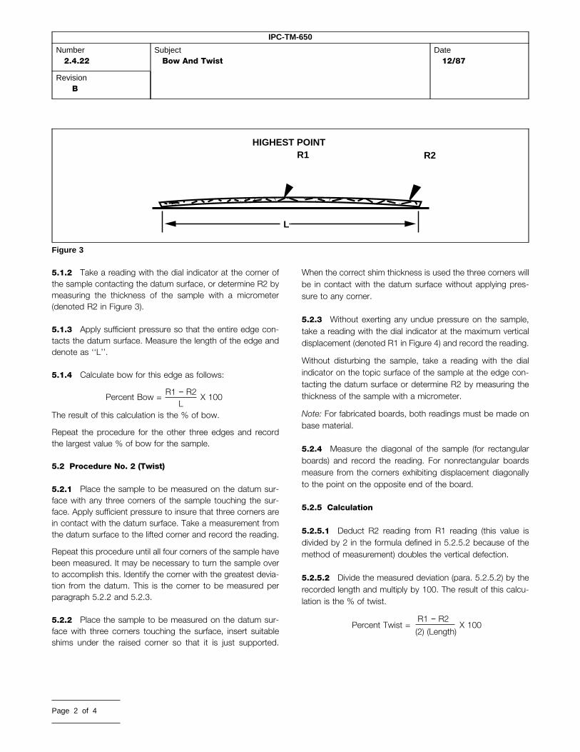
IPC-TM-650
Number2.4.22
SubjectBow And Twist
Date12/87
RevisionB
������ �L
R1 R2HIGHEST POINT
�����
Figure 35.1.2 Take a reading with the dial indicator at the corner ofthe sample contacting the datum surface, or determine R2 bymeasuring the thickness of the sample with a micrometer(denoted R2 in Figure 3).
5.1.3 Apply sufficient pressure so that the entire edge con-tacts the datum surface. Measure the length of the edge anddenote as ‘‘L’’.
5.1.4 Calculate bow for this edge as follows:
R1 − R2L
Percent Bow = X 100
The result of this calculation is the % of bow.
Repeat the procedure for the other three edges and recordthe largest value % of bow for the sample.
5.2 Procedure No. 2 (Twist)
5.2.1 Place the sample to be measured on the datum sur-face with any three corners of the sample touching the sur-face. Apply sufficient pressure to insure that three corners arein contact with the datum surface. Take a measurement fromthe datum surface to the lifted corner and record the reading.
Repeat this procedure until all four corners of the sample havebeen measured. It may be necessary to turn the sample overto accomplish this. Identify the corner with the greatest devia-tion from the datum. This is the corner to be measured perparagraph 5.2.2 and 5.2.3.
5.2.2 Place the sample to be measured on the datum sur-face with three corners touching the surface, insert suitableshims under the raised corner so that it is just supported.
��������
Page 2 of 4
When the correct shim thickness is used the three corners willbe in contact with the datum surface without applying pres-sure to any corner.
5.2.3 Without exerting any undue pressure on the sample,take a reading with the dial indicator at the maximum verticaldisplacement (denoted R1 in Figure 4) and record the reading.
Without disturbing the sample, take a reading with the dialindicator on the topic surface of the sample at the edge con-tacting the datum surface or determine R2 by measuring thethickness of the sample with a micrometer.
Note: For fabricated boards, both readings must be made onbase material.
5.2.4 Measure the diagonal of the sample (for rectangularboards) and record the reading. For nonrectangular boardsmeasure from the corners exhibiting displacement diagonallyto the point on the opposite end of the board.
5.2.5 Calculation
5.2.5.1 Deduct R2 reading from R1 reading (this value isdivided by 2 in the formula defined in 5.2.5.2 because of themethod of measurement) doubles the vertical defection.
5.2.5.2 Divide the measured deviation (para. 5.2.5.2) by therecorded length and multiply by 100. The result of this calcu-lation is the % of twist.
R1 − R2
(2) (Length)Percent Twist = X 100
�����
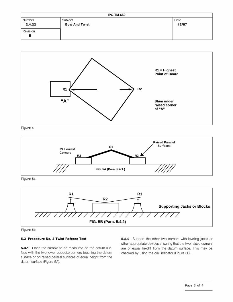
IPC-TM-650
Number2.4.22
SubjectBow And Twist
Date12/87
RevisionB
Figure 4
R1 R2
“A”
R1 = HighestPoint of Board
Shim underraised cornerof “A”
Figure 5a
▼R2 Lowest Corners
R2 R2
R1
Raised Parallel Surfaces
FIG. 5A (Para. 5.4.1.)
Figure 5b
R1 R1R2
Supporting Jacks or Blocks
FIG. 5B (Para. 5.4.2)
5.3 Procedure No. 3 Twist Referee Test
5.3.1 Place the sample to be measured on the datum sur-face with the two lower opposite corners touching the datumsurface or on raised parallel surfaces of equal height from thedatum surface (Figure 5A).
5.3.2 Support the other two corners with leveling jacks orother appropriate devices ensuring that the two raised cornersare of equal height from the datum surface. This may bechecked by using the dial indicator (Figure 5B).
Page 3 of 4
IPC-TM-650
Number2.4.22
SubjectBow And Twist
Date12/87
RevisionB
Figure 5c
(5.4.3) Measure at This Point
(5.4.4) Measure at This Point
R2R2
R1
5.3.3 With the dial indicator, measure the highest raisedportion on the board and record the reading as R1 (Figure5C).
5.3.4 Without disturbing the sample, take a reading with thedial indicator on one of the corners contacting the surface (R2)and record the reading (Figure 5C).
5.3.5 Measure the diagonal of the sample (for rectangularboards) and record the reading. For nonrectangular boardsmeasure from the corner exhibiting maximum displacementdiagonally to the point on the opposite end of the board.
5.3.6 Calculation
5.3.6.1 Deduct the measurement R2 from the measurementR1. This difference is denoted as twist.
5.3.6.2 Divide the measured deviation (para. 5.3.6.1) by therecorded length and multiply by 100. The result of this calcu-lation is the % of twist.
Percent Twist = R1 – R2L
X 100
Figure 6
Page 4 of 4
5.4 Procedure 4, Production Testing (Bow and Twist)
Having previously determined the maximum allowable devia-tion of a board from a flat plane, the following GO-NO GOprocedures may be used.
5.4.1 With both corners of an edge touching the datum sur-face and using a suitable known dimensional standard suchas a pin gauge or feeler gauge, conforming to the maximumallowable deviation (5.4), attempt to insert the gauge betweenthe raised portion of the board and the datum surface(Figure 6).
5.4.2 Attempt to insert gauge conforming to the allowablesurface dimension between the raised edge of the board andthe datum (Figure 7).
5.4.3 If the gauge does not enter the gap, the board willhave met the bow/twist criteria.
5.5 Notes
5.5.1 Forms of distortion other than as defined in this testmethod (such as multiple convolutions) cannot be evaluatedaccurately by these test methods and therefore should receivespecial attention.
Figure 7

Standard Improvement Form IPC-2221The purpose of this form is to provide theTechnical Committee of IPC with inputfrom the industry regarding usage ofthe subject standard.
Individuals or companies are invited tosubmit comments to IPC. All commentswill be collected and dispersed to theappropriate committee(s).
If you can provide input, please completethis form and return to:IPC2215 Sanders RoadNorthbrook, IL 60062-6135Fax 847 509.9798
1. I recommend changes to the following:
Requirement, paragraph number
Test Method number , paragraph number
The referenced paragraph number has proven to be:
Unclear Too Rigid In Error
Other
2. Recommendations for correction:
3. Other suggestions for document improvement:
Submitted by:
Name Telephone
Company E-mail
Address
City/State/Zip Date

This page intentionally left blank

ANSI/IPC-T-50 Terms and Definitionsfor Interconnecting and Packaging Electronic CircuitsDefinition Submission/Approval SheetThe purpose of this form is to keepcurrent with terms routinely usedin the industry and their definitions.Individuals or companies are invitedto comment. Please complete thisform and return to:
IPC2215 Sanders RoadNorthbrook, IL 60062-6135Fax: 847-509-9798
SUBMITTOR INFORMATION:
Name:
Company:
City:
State/Zip:
Telephone:
Date:
❑ This is a NEW term and definition being submitted.❑ This is an ADDITION to an existing term and definition(s).❑ This is a CHANGE to an existing definition.
Term Definition
If space not adequate, use reverse side or attach additional sheet(s).
Artwork: ❑ Not Applicable ❑ Required ❑ To be supplied
❑ Included: Electronic File Name:
Document(s) to which this term applies:
Committees affected by this term:
Office UseIPC Office Committee 2-30
Date Received:Comments Collated:Returned for Action:Revision Inclusion:
Date of Initial Review:Comment Resolution:Committee Action: ❑ Accepted ❑ Rejected
❑ Accept Modify
IEC ClassificationClassification Code • Serial Number
Terms and Definition Committee Final Approval Authorization:Committee 2-30 has approved the above term for release in the next revision.
Name: Committee: Date:IPC 2-30
THE INSTITUTE FOR
INTERCONNECTING
AND PACKAGING
ELECTRONIC CIRCUITS

This page intentionally left blank

Technical QuestionsThe IPC staff will research your technical question and attempt to find an appropriate specification interpretation ortechnical response. Please send your technical query to the technical department via:
tel 847/509-9700 fax 847/509-9798 http://www.ipc.org e-mail: [email protected]
IPC Technical ForumsIPC technical forums are opportunities to network on the Internet. It’s the best way to get the help you need today!Over 2,500 people are already taking advantage of the excellent peer networking available through e-mail forumsprovided by IPC. Members use them to get timely, relevant answers to their technical questions.
[email protected] forum is for discussion of technical help, comments or questions on IPC specifications, or other technicalinquiries. IPC also uses TechNet to announce meetings, important technical issues, surveys, etc.
[email protected] forum is for discussion of flip chip and related chip scale semiconductor packaging technologies. It iscosponsored by the National Electronics Manufacturing Initiative (NEMI).
[email protected] forum covers environmental, safety and related regulations or issues.
[email protected] Council forum covers information on upcoming IPC Designers Council activities as well as information,comment, and feedback on current design issues,local chapter meetings, new chapters forming, and other designtopics.
[email protected] IPC Roadmap forum is the communication vehicle used by members of the Technical Working Groups (TWGs)who develop the IPC National Technology Roadmap for Electronic Interconnections.
[email protected] peer networking forum is specific to solder mask qualification and use.
ADMINISTERING YOUR SUBSCRIPTION STATUS:All commands (such as subscribe and signoff) must be sent to [email protected]. Please DO NOT send any command tothe mail list address, (i.e.<mail list> @ipc.org), as it would be distributed to all the subscribers.
Example for subscribing: Example for signing off:To: [email protected] To: [email protected]: Subject:Message: subscribe TechNet Joseph H. Smith Message: sign off DesignerCouncil
Please note you must send messages to the mail list address ONLY from the e-mail addressto which you want to apply changes. In other words,if you want to sign off the mail list, you must send the signoffcommand from the address that you want removed from the mail list. Many participants find it helpful to signoff a listwhen travelling or on vacation and to resubscribe when back in the office.
How to post to a forum:To send a message to all the people currently subscribed to the list, just send to <mail list>@ipc.org Please note, usethe mail list address that you want to reach in place of the <mail list> string in the above instructions.
Example:To: [email protected]: <your subject>Message: <your message>
The associated e-mail message text will be distributed to everyone on the list, including the sender. Furtherinformation on how to access previous messages sent to the forums will be provided upon subscribing.
For more information, contact Dmitriy Sklyartel 847/509-9700 x311 fax 847/509-9798e-mail: [email protected] http://www.ipc.org/html/forum.htm

IPC World Wide Web Page http://www.ipc.orgOur home page provides access to information about upcoming events, publications and videos, membership, andindustry activities and services. Visit soon and often.
Education and TrainingIPC conducts local educational workshops and national conferences to help you better understand emergingtechnologies. National conferences have covered Ball Grid Array and Flip Chip/Chip Scale Packaging. Some workshoptopics include:
Printed Wiring Board Fundamentals High Speed DesignTroubleshooting the PWB Manufacturing Process Design for ManufacturabilityChoosing the Right Base Material Laminate Design for AssemblyAcceptability of Printed Boards Designers Certification PreparationNew Design Standards
IPC video tapes and CD-ROMs can increase your industry know-how and on the job effectiveness.
For more information on programs, contact John Rileytel 847/509-9700 ext. 308 fax 847/509-9798e-mail: [email protected] http://www.ipc.org
For more information on IPC Video/CD Training, contact Mark Pritchardtel 505/758-7937 ext. 202 fax 505/758-7938e-mail: [email protected]://www.ipc.org
Training and CertificationIPC-A-610 Training and Certification Program“The Acceptability of Electronic Assemblies” (ANSI/IPC-A-610) is the most widely used specification for the PWBassembly industry. An industry consensus Training and Certification program based on the IPC-A-610 is available toyour company.
For more information, contact John Rileytel 847/509-9700 ext. 308 fax 847/509-9798e-mail: [email protected] http://www.ipc.org/html/610.htm
IPC Printed Circuits ExpoIPC Printed Circuits Expo is the largest trade exhibition in North America devoted to the PWB industry. Over 90technical presentations make up this superior technical conference.
For more information, contact Kim Behrtel 847/509-9700 ext. 319 fax 847/509-9798e-mail: [email protected] http://www.ipc.org
How to Get InvolvedThe first step is to join IPC. An application for membership can be found on page 74.Once you become a member, the opportunities to enhance your competitiveness are vast. Join a technical committeeandlearn from our industry’s best while you help develop the standards for our industry. Participate in market researchprograms which forecast the future of our industry. Participate in Capitol Hill Day and lobby your Congressmen andSenators for better industry support. Pick from a wide variety of educational opportunities: workshops, tutorials, andconferences. More up-to-date details on IPC opportunities can be found on our web page: http:/www.ipc.org.
For information on how to get involved, contact:Jeanette Ferdman, Membership Managertel 847/509-9700 ext. 309 fax 847/509-9798e-mail: [email protected] http://www.ipc.org
March 16-18, 1999Long Beach, California
April 28-30, 1998Long Beach, California

A P P L I C A T I O N F O R S I T E M E M B E R S H I P
Our facility purchases, uses and/or manufactures printed wiring boards or other electronic interconnection products for our ownuse in a final product. Also known as original equipment manufacturers (OEM).
We are representatives of a government agency, university, college, technical institute who are directly concerned with design,research, and utilization of electronic interconnection devices. (Must be a non-profit or not-for-profit organization.)
n One-sided and two-sided rigid printedboards
n Multilayer printed boards
n Flexible printed boardsn Flat cablen Hybrid circuits
n Discrete wiring devicesn Other interconnections
IS YOUR INTEREST IN:
n purchasing/manufacture of printed circuit boards
n purchasing/manufacturing printed circuit assemblies
What is your company’s main product line? __________________________________________________________________
WHAT PRODUCTS DO YOU
MAKE FOR SALE?
n Turnkeyn SMTn Chip Scale Technology
n Through-holen Mixed Technology
n Consignmentn BGA
Our facility assembles printed wiring boards on a contract basis and/or offers other electronic interconnection products for sale.
Our facility supplies raw materials, machinery, equipment or services used in the manufacture or assembly of electronic inter-connection products.
Thank you for your decision to join IPC members on the “Intelligent Path to Competitiveness”! IPC Membership issite specific, which means that IPC member benefits are available to all individuals employed at the site designat-ed on the other side of this application.
To help IPC serve your member site in the most efficient manner possible, please tell us what your facility does bychoosing the most appropriate member category.
Our facility manufactures and sells to other companies, printed wiring boards or other electronic interconnection products onthe merchant market.
Name of Chief Executive Officer/President___________________________________________________________________
Name of Chief Executive Officer/President ________________________ _
What products do you supply?_____________________________________________________________________________
Please be sure both sides of this application are correctly completed
PLEASE CHECK
APPROPRIATE
CATEGORY
■
INDEPENDENTPRINTED BOARDMANUFACTURERS
■
INDEPENDENT
PRINTED BOARDASSEMBLERS
EMSI COMPANIES
■
OEM –MANUFACTURERSOF ANY ENDPRODUCTUSINGPCB/PCASOR CAPTIVEMANUFACTURERSOF PCBS/PCAS
■
INDUSTRYSUPPLIERS
■
GOVERNMENT
AGENCIES/ACADEMIC
TECHNICAL
LIAISONS

@@@@@@@@e?@@@@@@@@e?@@h?@@h?@@h?@@h?@@h?@@h?
@@@@@@@@e?@@@@@@@@?e@@@@@@@@e?@@@@@@@@?e@@@@@@@@e?@@@@@@@@?e@@@@@@@@e?@@@@@@@@?e@@@@@@@@e?@@@@@@@@?e@@@@@@@@e?@@@@@@@@?e@@@@@@@@e?@@@@@@@@?e@@@@@@@@e?@@@@@@@@?e@@@@@@@@e?@@@@@@@@?e@@@@@@@@e?@@@@@@@@?e@@@@@@@@e?@@@@@@@@?e@@@@@@@@e?@@@@@@@@?e@@@@@@@@e?@@@@@@@@?e@@@@@@@@e?@@@@@@@@?e@@@@@@@@e?@@@@@@@@?e@@@@@@@@e?@@@@@@@@?e@@@@@@@@e?@@@@@@@@?e@@@@@@@@e?@@@@@@@@?e@@@@@@@@e?@@@@@@@@?e@@@@@@@@e?@@@@@@@@?e@@@@@@@@e?@@@@@@@@e?@@@@@@@@?e@@@@@@@@e?@@@@@@@@?e@@@@@@@@e?@@@@@@@@?e@@@@@@@@e?@@@@@@@@?e@@@@@@@@e?@@@@@@@@?e@@@@@@@@e?@@@@@@@@?e@@@@@@@@e?@@@@@@@@?e@@@@@@@@e?@@@@@@@@?e@@@@@@@@e?@@@@@@@@?e@@@@@@@@e?@@@@@@@@?e@@@@@@@@e?@@@@@@@@?e@@@@@@@@e?@@@@@@@@?e@@@@@@@@e?@@@@@@@@?e@@@@@@@@e?@@@@@@@@?e@@@@@@@@e?@@@@@@@@?e@@@@@@@@e?@@@@@@@@?e@@@@@@@@e?@@@@@@@@?e@@@@@@@@e?@@@@@@@@?e@@@@@@@@e?@@@@@@@@?e@@@@@@@@e?@@@@@@@@?e@@@@@@@@e?
@@@@@@@@@@@@@@@@@@@@@@@@@@@@
@@@@@@@@@@@@@@@@
@@@@@@@@@@@@@@@@
@@@@@@@@@@@@@@@@
@@@@@@@@@@@@@@@@
@@@@@@@@@@@@@@@@
@@@@@@@@@@@@@@@@
@@@@@@@@@@@@@@@@
@@@@@@@@@@@@@@@@
@@@@@@@@@@@@@@@@
@@@@@@@@@@@@@@@@
@@@@@@@@@@@@@@@@
@@@@@@@@@@@@@@@@
@@@@@@@@@@@@@@@@
@@@@@@@@@@@@@@@@
@@@@@@@@@@@@@@@@
@@@@@@@@@@@@@@@@
@@@@@@@@@@@@@@@@
@@@@@@@@@@@@@@@@
@@@@@@@@@@@@@@@@
@@@@@@@@@@@@@@@@
@@@@@@@@@@@@@@@@
@@@@@@@@@@@@@@@@
@@@@@@@@@@@@@@@@
?@@?@@?@@?@@?@@?@@
?@@@@@@@@?@@@@@@@@
?@@@@@@@@?e@@@@@@@@e?@@@@@@@@?e@@@@@@@@e?@@@@@@@@?e@@@@@@@@e?@@@@@@@@?e@@@@@@@@e?@@@@@@@@?e@@@@@@@@e?@@@@@@@@?e@@@@@@@@e?@@@@@@@@?e@@@@@@@@e?@@@@@@@@?e@@@@@@@@e?@@@@@@@@?e@@@@@@@@e?@@@@@@@@?e@@@@@@@@e?@@@@@@@@?e@@@@@@@@e?@@@@@@@@?e@@@@@@@@e?@@@@@@@@?e@@@@@@@@e?@@@@@@@@?e@@@@@@@@e?@@@@@@@@?e@@@@@@@@e?@@@@@@@@?e@@@@@@@@e?@@@@@@@@?e@@@@@@@@e?@@@@@@@@?e@@@@@@@@e?@@@@@@@@?e@@@@@@@@e?@@@@@@@@?e@@@@@@@@e?@@@@@@@@?@@@@@@@@?e@@@@@@@@e?@@@@@@@@?e@@@@@@@@e?@@@@@@@@?e@@@@@@@@e?@@@@@@@@?e@@@@@@@@e?@@@@@@@@?e@@@@@@@@e?@@@@@@@@?e@@@@@@@@e?@@@@@@@@?e@@@@@@@@e?@@@@@@@@?e@@@@@@@@e?@@@@@@@@?e@@@@@@@@e?@@@@@@@@?e@@@@@@@@e?@@@@@@@@?e@@@@@@@@e?@@@@@@@@?e@@@@@@@@e?@@@@@@@@?e@@@@@@@@e?@@@@@@@@?e@@@@@@@@e?@@@@@@@@?e@@@@@@@@e?@@@@@@@@?e@@@@@@@@e?@@@@@@@@?e@@@@@@@@e?@@@@@@@@?e@@@@@@@@e?@@@@@@@@?e@@@@@@@@e?@@@@@@@@?e@@@@@@@@e?@@@@@@@@
@@g@@g@@g@@g@@g@@g@@@@@@@@@@@@@@@@
@@@@@@@@@@@@@@@@
@@@@@@@@@@@@@@@@
@@@@@@@@@@@@@@@@
@@@@@@@@@@@@@@@@
@@@@@@@@@@@@@@@@
@@@@@@@@@@@@@@@@
@@@@@@@@@@@@@@@@
@@@@@@@@@@@@@@@@
@@@@@@@@@@@@@@@@
@@@@@@@@@@@@@@@@
@@@@@@@@@@@@@@@@
@@@@@@@@@@@@@@@@
@@@@@@@@@@@@@@@@
@@@@@@@@@@@@@@@@
@@@@@@@@@@@@@@@@
@@@@@@@@@@@@@@@@
@@@@@@@@@@@@@@@@
@@@@@@@@@@@@@@@@
@@@@@@@@@@@@@@@@
@@@@@@@@@@@@@@@@
@@@@@@@@@@@@@@@@
@@@@@@@@@@@@@@@@
@@@@@@@@@@@@@@@@
PLEASE ATTACH BUSINESS CARD
OF OFFICIAL REPRESENTATIVE HERE
Please check one:
❏ $1,000.00 Annual dues for Primary Site Membership (Twelve months of IPC membership begins from the time the applicationand payment are received)
❏ $800.00 Annual dues for Additional Facility Membership: Additional membership for a site within an organization whereanother site is considered to be the primary IPC member.
❏ $600.00** Annual dues for an independent PCB/PWA fabricator or independent EMSI provider with annual sales of less than$1,000,000.00. **Please provide proof of annual sales.
❏ $250.00 Annual dues for Government Agency/University/not-for-profit organization
TMRC Membership ❏ Please send me information on Membership in the Technology Marketing Research Council (TMRC)
AMRC Membership ❏ Please send me information for Membership in the Assembly Marketing Research Council (AMRC)
Mail application with check or money order to:
IPCDept. 77-3491Chicago, IL 60678-3491
Fax/Mail application with credit card payment to:
IPC2215 Sanders RoadNorthbrook, IL 60062-6135Tel: 847 509.9700Fax: 847 509.9798
Payment Information
Enclosed is our check for $
Please bill my credit card: (circle one) MC AMEX VISA DINERS
Card No. Exp date ____________________
Authorized Signature
Site Information:
Company Name
Street Address
City State Zip Country
Main Phone No. Fax
Primary Contact Name
Title Mail Stop
Phone Fax e-mail
Alternate Contact Name
Title Mail Stop
Phone Fax e-mail
A P P L I C A T I O N F O R S I T E M E M B E R S H I P

2215 Sanders RoadNorthbrook, Illinois60062-6135
TelFaxURL:
847 509.9700847 509.9798http://www.ipc.org
ISBN #1-580981-76-3